
 Open Access Article
 This Open Access Article is licensed under a Creative Commons Attribution-Non Commercial 3.0 Unported Licence
Self-aligned placement and detection of quantum dots on the tips of individual conical plasmonic nanostructures
Julia
Fulmes
*a,
Regina
Jäger
b,
Annika
Bräuer
a,
Christian
Schäfer
a,
Sebastian
Jäger
b,
Dominik A.
Gollmer
a,
Andreas
Horrer
a,
Elke
Nadler
b,
Thomas
Chassé
b,
Dai
Zhang
b,
Alfred J.
Meixner
b,
Dieter P.
Kern
a and
Monika
Fleischer
*a
aInstitute for Applied Physics, Eberhard Karls University of Tübingen and Center LISA+, Auf der Morgenstelle 10, 72076 Tübingen, Germany. E-mail: julia.fulmes@yahoo.de; monika.fleischer@uni-tuebingen.de
bInstitute of Physical and Theoretical Chemistry, Eberhard Karls University of Tübingen and Center LISA+, Auf der Morgenstelle 18, 72076 Tübingen, Germany
First published on 17th August 2015
Abstract
Hybrid structures of few or single quantum dots (QDs) coupled to single optical antennas are of prime interest for nano-optical research. The photoluminescence (PL) signal from single nanoemitters, such as QDs, can be enhanced, and their emission characteristics modified, by coupling them to plasmonic nanostructures. Here, a self-aligned technique for placing nanoscale QDs with about 10 nm lateral accuracy and well-defined molecular distances to the tips of individual nanocones is reported. This way the QDs are positioned exactly in the high near-field region that can be created near the cone apex. The cones are excited in the focus of a radially polarized laser beam and the PL signal of few or single QDs on the cone tips is spectrally detected.
Introduction
In this work we present a hybrid system consisting of few or single quantum dots (QDs) near the tips of plasmonic nanocones. The unique optical properties of QDs, such as broad absorption and narrow emission bands, bright and stable photoluminescence (PL), and a size-tuneable emission wavelength, make them promising for various applications.1 QDs are very interesting for nanophotonics and quantum optics, in which they serve as single photon sources.2 They also play an important role as tags and markers in biological sensing.3In metal nanoparticles collective oscillations of the conduction electrons, known as localized surface plasmons, can be excited by an external field.4 The plasmons mediate strong interactions between the incoming light and the nanostructure, enabling the straightforward detection of individual structures in a far-field optical microscope.5 The positioning of quantum emitters in the vicinity of the high near-field regions of such metal structures, which act as optical antennas, results in energy transfer between the two objects6 and may lead to quenching or enhancement of the QD signal.7,8
The PL intensity of QDs in the vicinity of such optical antennas can be enhanced if their spectral properties are well matched. For this reason, it is essential to have the ability to fabricate nanostructures with appropriate spectral properties in a reproducible manner. Gold cones with dimensions on the order of 100 nm are highly suitable as optical antennas for visible light, because their specific resonance frequencies can be tuned by varying the material, size, shape and aspect ratio,9 and they feature an easily accessible strong near-field region near the tip.10
The capability to place individual nanoobjects at precise locations on or near metallic nanostructures or patterned surfaces is highly desirable for a variety of practical applications. The positioning of nano-emitters with high accuracy is a key issue for photonic crystal cavities,11 waveguides for single-photon generation,12 quantum dot lasers,13 or nonlinear optical devices.14 Nanoscale placement of QDs has e.g. been demonstrated in the vicinity of metamaterial surfaces15 or metallic nanostructures.7 The placement of QDs within the high near-field regions of plasmonic structures requires a lateral accuracy on the order of 10 nm and less, and an accuracy relative to the surface on the nm scale. Single QDs are very difficult to manipulate due to their small sizes, and the positioning of particles with nm precision in general has proven to be a highly challenging task. Commonly used methods are optical tweezers,16 mechanical manipulators to push, pull, and place individual nanoparticles on a variety of surfaces,17 or overlay lithography.18–20 However, these methods are time-consuming for practical realisation, chemically non-selective, or sensitive to their environment. Other methods, such as the chemical functionalization of structures, show high selectivity but low statistical placement reproducibility.21
We present an innovative and straightforward self-alignment method of cone embedding with subsequent uncovering of the tips, which permits to place QDs with good accuracy in the hot-spots around the apexes of plasmonic nanocones. Gold cones with localized surface plasmon resonances matched to the emission wavelengths of QDs are fabricated. Immobilization of QDs in the active region of the plasmonic structures is realized at molecular distances to the uncovered gold surface by a chemical functionalization process. Afterwards individual QDs coupled to the cone tips are optically detected.
Experimental
Cone fabrication
Different methods for the fabrication of metallic nanocones are described in literature.22–27 In this work arrays of gold nanocones in square lattices are fabricated on a glass substrate coated with a homogeneous 50 nm thick film of indium tin oxide (ITO) to avoid charge accumulation effects during electron beam lithography (EBL). The fabrication steps of cones are schematically shown in Fig. 1 together with typical scanning electron microscopy (SEM, Philips XL 30) images. First a polymethylmethacrylate (PMMA) positive resist layer is spin-coated onto the sample and patterned by EBL (SEM, Philips XL 30, 30 kV accelerating voltage) into nanohole arrays with periodicities of 2 μm, 1 μm, 500 nm and 250 nm. After the development process, oxygen plasma cleaning is applied to the sample in order to remove potential residues. During the subsequent thermal gold deposition the diameter of the nanoholes decreases gradually, leading to the growth of cone-shaped structures.22 After a lift-off process, homogeneous conical nanostructures with small tip radii about 10 nm remain.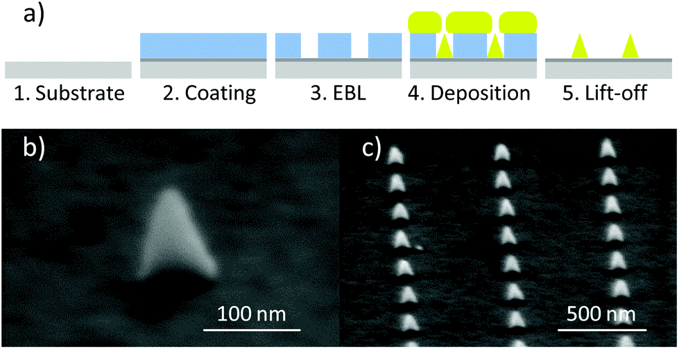 | ||
| Fig. 1 (a) Gold cone fabrication scheme: 1. Glass substrate; 2. sputtering of ITO and spin-coating of PMMA; 3. electron beam lithography; 4. growth of cones during the gold deposition process; 5. lift-off. (b) and (c) SEM images of gold cones, viewing angle 70° with respect to the surface normal: (b) single nanocone with a height of 100 nm and a base diameter of 75 nm, (c) array of gold nanocones with a height of about 100 nm and a spacing of 500 nm. | ||
Optical characterization and simulation
It has been shown in a number of studies that the PL signal from nano-emitters can be enhanced in the electric near-field of metallic nanostructures.28 Due to the special geometry of nanocones a strongly localized near-field is excited close to the apex. In order to visualize the distribution of the electric near-field enhancement simulations using the Finite Element Method based software COMSOL Multiphysics are performed. A strong enhancement of the electric near-field around the cone tip is predicted at the resonance wavelength by excitation with an electrical field Ez polarized along the cone axis (see Fig. 2a). Matching this condition experimentally can be achieved by confocal measurements using excitation with a focussed radially polarized laser mode.29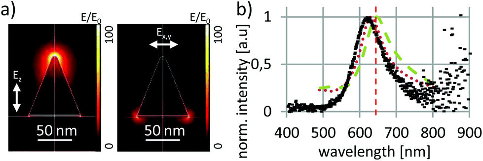 | ||
| Fig. 2 (a) Distribution of the enhanced electric near-field around a gold nanocone on ITO at the resonance wavelengths (646 nm and 632 nm) for excitation with light polarized along the cone axis (left) and along the cone base (right), simulated using COMSOL Multiphysics. (b) Measured scattering spectrum (black dots) and simulated in-plane (red dotted line) and out-of-plane (green dashed line) plasmon modes of a gold cone with a height of 100 nm and base diameter of 75 nm. The QD emission wavelength is marked by the vertical red dashed line. | ||
For the analysis of the optical properties of QDs, placed within the near-field of plasmonic nanocones, the localized surface plasmon resonance of the nanostructure is tuned to the quantum dot emission wavelength.6,30 In this hybrid system core–shell CdSe/ZnS QDs with an emission maximum at 650 nm are used. The plasmon properties of the gold cones with heights of 100 nm and base diameters of 75 nm were examined by single particle dark field spectroscopy. The plasmon resonance spectra of the cones consist in a superposition of dipolar in-plane and out-of-plane modes leading to an excitation of the cone base or tip, respectively (cf. Fig. 2a), where the in-plane mode is predominantly detected in the dark field configuration.9
Simulations of both the in- and the out-of-plane mode spectrum are shown in Fig. 2b together with a measured spectrum.
The experimentally relevant resonance of the out-of-plane mode (tip excitation) occurs around 646 nm in the simulation and can be seen in the measurement as a small shoulder or asymmetry shifted slightly to the long wavelength side of the dominant in-plane mode. The out-of-plane mode is well matched to the emission wavelength of the QDs.
Positioning and immobilization of quantum dots on the tips of individual conical plasmonic nanostructures
The strongly localized electric field close to the cone apex can improve signal detection from the nanoobjects linked to the cone tips. Therefore it is important to place the investigated objects (in our case QDs) with good accuracy near the cone tips, where the high near-field hotspot is located. An additional reason to place the QDs only at the cone tips is eliminating the background signal of randomly placed QDs on the substrate surface, which is inevitable for conventional methods such as spin-coating. This way the investigation of individual hybrid nanoobjects is enabled.The realization of selective QD positioning consists of embedding cones in a resist, which is stable against the QD solvent, and of the subsequent self-aligned removal of the resist from the tip of the cones. Then the unprotected surface of the cone tips is functionalized using thiol chemistry for immobilization of QDs only in the vicinity of the cone tips. Afterwards the resist is removed completely, resulting in free-standing gold nanocones with QDs at the tips. A schematic of the processing steps and typical SEM images (Philips XL 30) of gold cones after each single step are shown in Fig. 3.
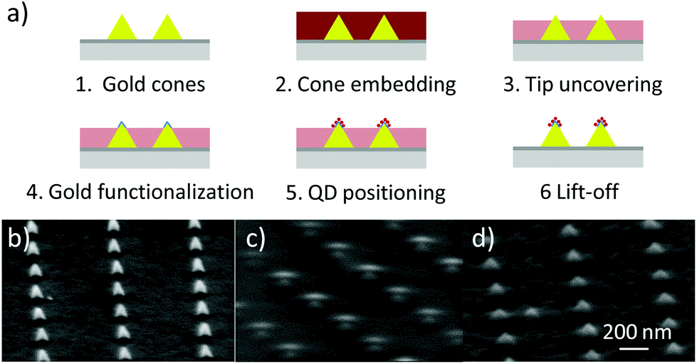 | ||
| Fig. 3 (a) Processing steps for the placement and immobilization of QDs on the tips of individual conical nanostructures: 1. Free-standing gold cones after fabrication; 2. embedding of the cones in resist; 3. uncovering the cone tips; 4. functionalization of the gold surface using thiol chemistry; 5. positioning of QDs on the cone tips; 6. resist removal. (b)–(d) SEM images of the individual steps of gold cone tip uncovering, demonstrating steps 1., 2. and 3. from (a), respectively. | ||
Taking into account that the covering resist should be unaffected by the QD solution, ma-P 1215 positive photoresist (Micro Resist Technology GmbH) was used for the CdSe/ZnS QDs in toluene solvent (Plasmachem GmbH). The layer thickness depends on the spin-coating rotation parameters and should be about 10 nm higher than the cones’ height to cover them completely. The ma-P 1215 resist was diluted with methoxypropyl acetate (MPA) (ma-P 1215![[thin space (1/6-em)]](https://www.rsc.org/images/entities/char_2009.gif) :MPA 1:5) to reach the desired thicknesses in the range of 70 nm to 130 nm (for typical cone heights of about 60 to 120 nm) with few nm accuracy. For example, 4000 rpm for 60 s results in 110 nm layer thickness, applied to 100 nm high gold cones. After spin-coating the resist was pre-baked for 60 s at 120 °C and exposed by UV-light (175 W) for 4 s. In a subsequent development step, using water diluted MAD-331 developer (Micro Resist Technology GmbH, MAD-331:H2O 1:3) for 45 s, 20 nm of the resist thickness was removed. The sharp cone apexes increase the exposure effect, leading in combination with the slow development to the controlled uncovering of the cone tips. To eliminate potential residues at the cone tips and to activate the gold surface, oxygen plasma cleaning (100 W, 0.4 mbar, 15 s) is applied. After the uncovering of the cone tips, only about 10 nm at the top of the cones are laid open.
:MPA 1:5) to reach the desired thicknesses in the range of 70 nm to 130 nm (for typical cone heights of about 60 to 120 nm) with few nm accuracy. For example, 4000 rpm for 60 s results in 110 nm layer thickness, applied to 100 nm high gold cones. After spin-coating the resist was pre-baked for 60 s at 120 °C and exposed by UV-light (175 W) for 4 s. In a subsequent development step, using water diluted MAD-331 developer (Micro Resist Technology GmbH, MAD-331:H2O 1:3) for 45 s, 20 nm of the resist thickness was removed. The sharp cone apexes increase the exposure effect, leading in combination with the slow development to the controlled uncovering of the cone tips. To eliminate potential residues at the cone tips and to activate the gold surface, oxygen plasma cleaning (100 W, 0.4 mbar, 15 s) is applied. After the uncovering of the cone tips, only about 10 nm at the top of the cones are laid open.
The resist removal step is necessary because if a resist layer with a thickness 10 nm less than the cone height was spin-coated directly, the resist would follow the topography, and a thin layer would remain on the cones.
To immobilize QDs on the cone tips they should chemically bind to the unprotected cone surface.31 For this reason 3-mercaptopropionic acid (3-MPA) was adsorbed on the gold surface (10 mM 3-MPA in water solution, 30 min) forming a self-assembled monolayer on the gold cone tips. The CdSe/ZnS QDs are capped with trioctylphosphine oxide (TOPO) and hexadecylamine (HDA) ligands, which act as binding and stabilizing agents and link to 3-MPA. The sample with functionalized gold cone tips was placed for 24 h in a 5 μg ml−1 solution of QDs in toluene (to allow binding to the surface) before rinsing to remove excess QDs. Afterwards the resist mask was removed by lift-off in acetone. The binding by thiol chemistry (3-MPA with TOPO/HDA, ∼3 nm long) immobilizes the QDs at the cone tips and provides a spacer between the QDs and gold surface. The chemical spacer in combination with the 0.7 nm thick ZnS QD shell is supposed to provide a sufficient distance to avoid quenching processes.32 Furthermore the spacer size can be easily varied by choosing different functionalizing molecules or QD shell thicknesses.
In the initial experiments, an estimated 70% of the cones showed evidence of one or more QDs being attached to their tips. It is expected that this rate can be even further optimized in future.
Results and discussion
PL measurements of QDs on cone tips
The PL properties of the hybrid structures are investigated in a home-built inverted confocal microscope using higher order doughnut-shaped laser modes. For these measurements a radially polarized (RP) cylindrical vector beam (λ = 488 nm) is utilized. The electric field distribution of the RP laser mode in the focus consists of a transversal (perpendicular to the optical axis) and a strong longitudinal (parallel to the optical axis) component.33 The PL images are obtained by raster scanning the sample through a focused RP beam. The position dependent PL intensity signal generated in the focus is detected by a single-photon counting avalanche photodiode (APD), while the laser excitation wavelength is cut off by a long pass filter. The spectra are collected via a spectrograph (Princeton Instruments, Acton SP 300i) with a CCD camera (Princeton Instruments, SPEC-10). A more detailed description of the setup can be found elsewhere.34The hybrid structures were imaged directly after their preparation. In the image scans, illustrated in Fig. 4a, all cones can be discerned by their (spectrally broad) luminescence. The signal seems to result mostly from some thin residual resist with enhanced luminescence at the cone locations, while cones decorated with QDs exhibit stronger PL intensities. Exemplarily the background corrected spectra obtained from three cones are investigated in more detail. In Fig. 4a, cone 1 and cone 3 show stronger PL than cone 2. The spectral distribution of the PL measured on the same three cones, shown in Fig. 4b, clearly demonstrates the origin of the different intensities. Cones 1 and 3 feature sharp peaks at the wavelength of the QD emission, corresponding to luminescence from single or few QDs. Cone 2 features a broad peak at shorter wavelengths resulting from the luminescence of the cone, which appears in the spectra of cone 1 and cone 3 as well. Comparing the optical properties with SEM images (Hitachi SU8030) of the same cones (Fig. 4c), it can be clearly seen that cone 1 is covered with several QDs. This may explain the distinct broadening of the corresponding spectrum. On cone 3, only at the very tip one or few QDs can be observed, resulting in a narrow spectrum. Cone 2 shows a bare gold surface without any QDs. While further experiments, such as correlation studies, would be required to establish that cone 3 is indeed coupled to a single QD, the spectral shape and full-width-at-half-maximum are indicative of a single emitter, denoting the potential to address the single QD regime.
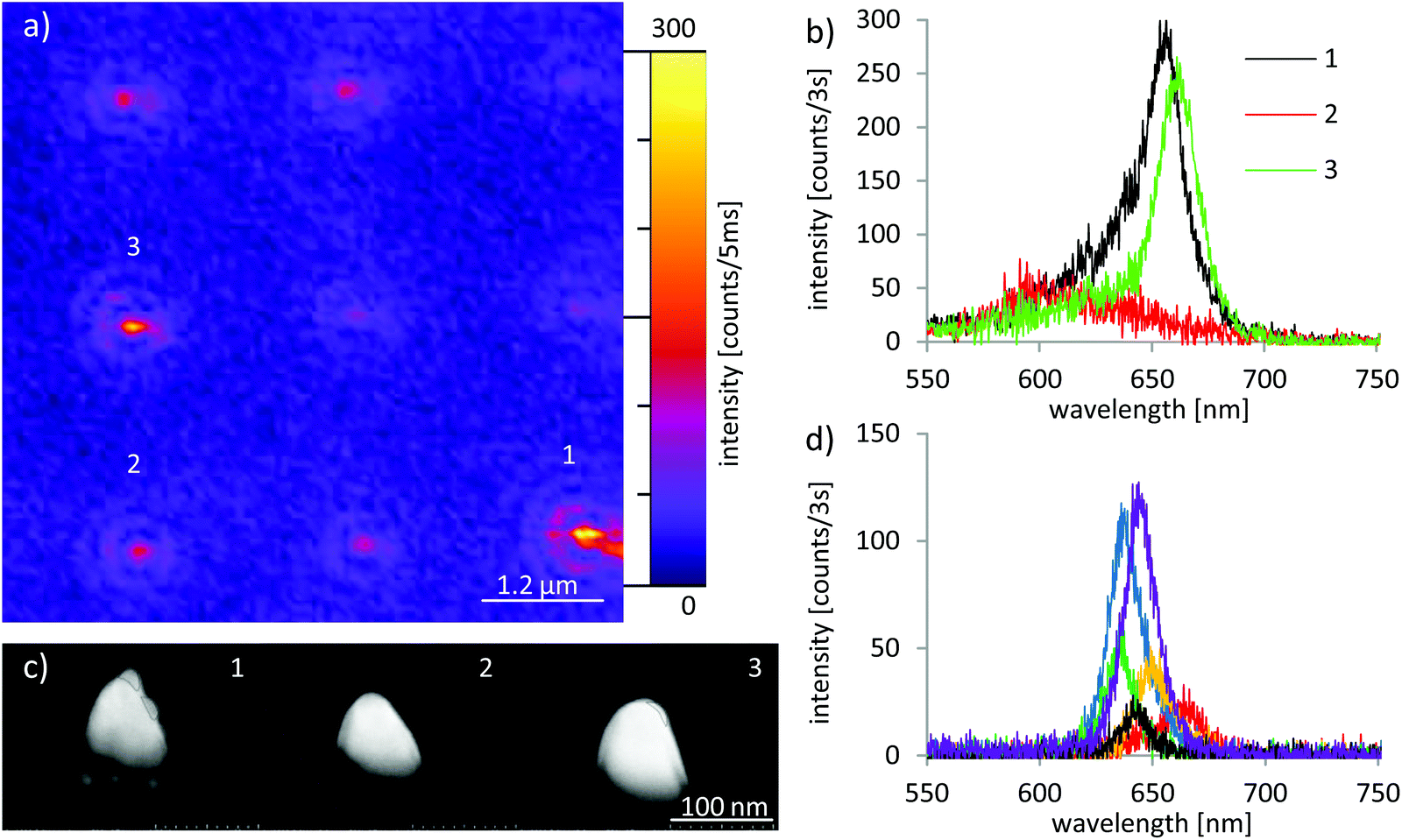 | ||
| Fig. 4 Detection of QDs linked to the tips of individual cones: (a) PL image of an array of cones with CdSe/ZnS QDs placed near the apexes of nanostructures (1) and (3) under excitation with a radially polarized laser beam. (b) Spectra of the three individual cones with (1, 3) and without (2) CdSe/ZnS QDs linked to the tips. The narrow peak around 650 nm originates from QD emission. The PL intensity and spectral width strongly depend on the number of bound QDs. (c) SEM images of the same gold nanocones with (1) few, (2) no, (3) one or few QDs. Viewing angle 45° with respect to the surface normal. The QDs are outlined for better clarity. (d) Typical spectra of single QDs on a glass cover slide. | ||
To compare the spectra obtained from the hybrid structures with spectra from single QDs, a dilution of the QD solution in toluene was spin-coated onto a glass cover slide and investigated under the same conditions as the hybrid structures. Fig. 4d shows typical background corrected spectra taken from six single QDs. The single QDs exhibit strong intensity variations during the acquisition time.
An indication for the different behaviour of the QDs close to the cone tip is the change in blinking, which seems to be less expressed in the vicinity of the gold cones. Similar effects have been reported for QDs near gold particles before.35–37 Intensity trajectories of the spectrally integrated PL were recorded from single QDs on glass and from QDs in hybrid systems using the APD followed by single-photon counting electronics. Two exemplary traces are shown in Fig. 5. It can be clearly seen that the QD on the nanocone in Fig. 5b shows longer bright intervals and a higher maximum intensity than the single QD on the substrate in Fig. 5a. Fig. 5b also gives a strong indication that single QDs can indeed be obtained on single nanocones with the present approach. The time trace exhibits pronounced binary on-off statistics that are a characteristic signature for the presence of an individual active QD.
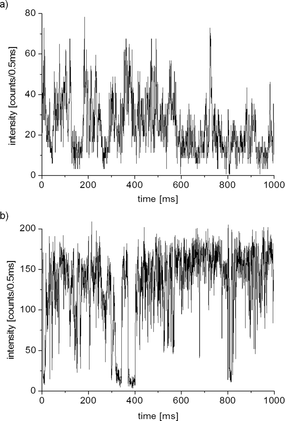 | ||
| Fig. 5 Experimental time traces (a) of a single QD on glass substrate, (b) two-level blinking of a single QD on a nanocone. Note the different intensity scales. | ||
These preliminary experiments indicate a significant intensity enhancement of the spectra originating from hybrid structures. However, to fully analyse the system, a direct quantitative comparison of the spectra will not suffice. Further research on these hybrid structures including life-time measurements will bring new insights into the energy transfer between the closely coupled cones and QDs. The gold nanocones with a tuneable plasmon resonance present an interesting and promising model for the analysis of optical processes in hybrid structures.
Conclusions
In summary, we present the preparation of novel hybrid nanostructures composed of single gold nanocones and CdSe/ZnS quantum dots (QDs) coupled to their tips. After the nanocone fabrication, the cones are embedded in a resist, followed by uncovering of the tips. The cone tips are chemically functionalized to immobilize the QDs in the next step. Finally, the resist is removed. This self-aligned process allows attaching QDs at a defined distance to the tips of individual cones with a lateral accuracy of about 10 nm. The hybrid system is chosen such that the plasmon resonance of the cone, accompanied by a strong electric near-field at the tip, is matched to the emission wavelength of the QDs. For such a system controlled emission of QDs through the coupling to the plasmonic structure is expected.6,30 First optical experiments indicate an enhanced QD emission in the hybrid structure compared to single QDs and a change in their blinking behaviour. The characteristic two-level blinking of single QDs is observed in time traces of the hybrid structure intensity, demonstrating the potential of this method to reach the single QD regime. Further investigations of the optical properties of this system will follow. The use of a hybrid system of QDs on a conical antenna may lead to an improved understanding of the interactions between QDs and plasmonic nanostructures and the manipulation of QD emission.Acknowledgements
J. F. gratefully acknowledges financial support by the Carl-Zeiss-Foundation. Financial support by the German-Israeli Foundation for Scientific Research and Development is gratefully acknowledged. We also acknowledge the Deutsche Forschungsgemeinschaft (Grant ME/1600 12-1). This work was performed in the context of the COST Action MP1302 Nanospectroscopy.Notes and references
- D. Bera, L. Qian, T. K. Tseng and P. H. Holloway, Materials, 2010, 3, 2260 CrossRef CAS PubMed.
- C. T. Yuan, P. Yu, H. C. Ko, J. Huang and J. Tang, ACS Nano, 2009, 3(10), 3051 CrossRef CAS PubMed.
- A. Hatef, S. M. Sadeghi, É. Boulais and M. Meunier, Nanotechnology, 2013, 24, 015502 CrossRef PubMed.
- U. Kreibig and M. Vollmer, Optical Properties of Metal Clusters, Springer, Berlin, 1995 Search PubMed.
- C. Sönnichsen, T. Franzl, T. Wilk, G. von Plessen, J. Feldmann, O. Wilson and P. Mulvaney, Phys. Rev. Lett., 2002, 88(7), 077402 CrossRef.
- A. G. Curto, T. H. Taminiau, G. Volpe, M. P. Kreuzer, R. Quidant and N. F. van Hulst, Nat. Commun., 2013, 4, 1750 CrossRef PubMed.
- P. Viste, J. Plain, R. Jaffiol, A. Vial, P. M. Adam and P. Royer, ACS Nano, 2010, 4(2), 759 CrossRef CAS PubMed.
- A. M. Kern, D. Zhang, M. Brecht, A. I. Chizhik, A. V. Failla, F. Wackenhut and A. J. Meixner, Chem. Soc. Rev., 2014, 43, 1263 RSC.
- C. Schäfer, D. A. Gollmer, A. Horrer, J. Fulmes, A. Weber-Bargioni, S. Cabrini, P. J. Schuck, D. P. Kern and M. Fleischer, Nanoscale, 2013, 5, 7861 RSC.
- M. Fleischer, C. Stanciu, F. Stade, J. Stadler, K. Braun, A. Heeren, M. Haeffner, D. P. Kern and A. J. Meixner, Appl. Phys. Lett., 2008, 93, 111114 CrossRef PubMed.
- K. Hennessy, A. Badolato, P. M. Petroff and E. Hu, Photon. Nanostruct. – Fundam. Appl., 2004, 2(2), 65 CrossRef PubMed.
- C. J. Wang, L. Huang, B. A. Parviz and L. Y. Lin, Nano Lett., 2006, 6(11), 2549 CrossRef CAS PubMed.
- D. L. Huffaker, G. Park, Z. Zou, O. B. Shchekin and D. G. Deppe, Appl. Phys. Lett., 1998, 73, 2564 CrossRef CAS PubMed.
- I. Fushman, D. Englund, A. Faraon, N. Stoltz, P. Petroff and J. Vučković, Science, 2008, 320, 769 CrossRef CAS PubMed.
- N. Engheta, Science, 2007, 317, 1698 CrossRef CAS PubMed.
- J. Do, R. Schreiber, A. A. Lutich, T. Liedl, J. Rodríguez-Fernández and J. Feldmann, Nano Lett., 2012, 12(9), 5008 CrossRef CAS PubMed.
- T. van der Sar, E. C. Heeres, G. M. Dmochowski, G. de Lange, L. Robledo, T. H. Oosterkamp and R. Hanson, Appl. Phys. Lett., 2009, 94, 173104 CrossRef PubMed.
- M. Piliarik, P. Kvasnička, N. Galler, J. R. Krenn and J. Homola, Opt. Express, 2011, 19(10), 9213 CrossRef CAS PubMed.
- M. Pfeiffer, K. Lindfors, H. Zhang, B. Fenk, F. Phillipp, P. Atkinson, A. Rastelli, O. G. Schmidt, H. Giessen and M. Lippitz, Nano Lett., 2014, 14(1), 197 CrossRef CAS PubMed.
- A. G. Curto, G. Volpe, T. H. Taminiau, M. P. Kreuzer, P. Quidant and N. F. van Hulst, Science, 2010, 329(5994), 930 CrossRef CAS PubMed.
- P. Zijlstra, P. M. R. Paulo, K. Yu, Q.-H. Xu and M. Orrit, Angew. Chem., Int. Ed., 2012, 51, 8352 CrossRef CAS PubMed.
- H. Fredriksson, Y. Alaverdyan, A. Dmitriev, C. Langhammer, D. S. Sutherland, M. Zäch and B. Kasemo, Adv. Mater., 2007, 19(23), 4297 CrossRef CAS PubMed.
- M. Fleischer, F. Stade, A. Heeren, M. Häffner, K. Braun, C. Stanciu, R. Ehlich, J. K. H. Hörber, A. J. Meixner and D. P. Kern, Microelectron. Eng., 2009, 86, 1219 CrossRef CAS PubMed.
- M. Fleischer, D. Zhang, K. Braun, S. Jäger, R. Ehlich, M. Häffner, C. Stanciu, J. K. H. Hörber, A. J. Meixner and D. P. Kern, Nanotechnology, 2010, 21, 065301 CrossRef CAS PubMed.
- M. Fleischer, A. Weber-Bargioni, S. Cabrini and D. P. Kern, Microelectron. Eng., 2011, 88(8), 2247 CrossRef CAS PubMed.
- A. Horrer, C. Schäfer, K. Broch, D. A. Gollmer, J. Rogalski, J. Fulmes, D. Zhang, A. J. Meixner, F. Schreiber, D. P. Kern and M. Fleischer, Small, 2013, 9(23), 3987 CrossRef CAS PubMed.
- J. M. Kontio, J. Simonen, J. Tommila and M. Pessa, Microelectron. Eng., 2010, 87, 17115 CrossRef PubMed.
- J. N. Farahani, D. W. Pohl, H.-J. Eisler and B. Hecht, Phys. Rev. Lett., 2005, 95, 017402 CrossRef CAS.
- Q. Zhan, Adv. Opt. Photon., 2009, 1, 1 CrossRef CAS.
- J.-H. Song, T. Atay, S. Shi, H. Urabe and A. V. Nurmikko, Nano Lett., 2005, 5(8), 1557 CrossRef CAS PubMed.
- J. T. Hugall, J. J. Baumberg and S. Mahajan, Appl. Phys. Lett., 2009, 95, 141111 CrossRef PubMed.
- P. Anger, P. Bharadwaj and L. Novotny, Phys. Rev. Lett., 2006, 96, 113002 CrossRef.
- R. Dorn, S. Quabis and G. Leuchs, Phys. Rev. Lett., 2003, 91, 233901 CrossRef CAS.
- A. M. Chizhik, R. Jäger, A. I. Chizhik, S. Bär, H.-G. Mack, M. Sackrow, C. Stanciu, A. Lyubimtsev, M. Hanack and A. J. Meixner, Phys. Chem. Chem. Phys., 2011, 13, 1722 RSC.
- Y. Ito, K. Matsuda and Y. Kanemitsu, Phys. Rev. B: Condens. Matter, 2007, 75, 033309 CrossRef.
- X. Ma, H. Tan, T. Kipp and A. Mews, Nano Lett., 2010, 10, 4166 CrossRef CAS PubMed.
- D. Ratchford, F. Shafiei, S. Kim, S. K. Gray and X. Li, Nano Lett., 2011, 11, 1049 CrossRef CAS PubMed.
| This journal is © The Royal Society of Chemistry 2015 |