
 Open Access Article
 This Open Access Article is licensed under a
 Creative Commons Attribution 3.0 Unported Licence
A silicon nanocrystal/polymer nanocomposite as a down-conversion layer in organic and hybrid solar cells†
V.
Svrcek
*a,
T.
Yamanari
a,
D.
Mariotti
b,
S.
Mitra
b,
T.
Velusamy
b and
K.
Matsubara
a
aResearch Center for Photovoltaic Technologies, National Institute of Advanced Industrial Science and Technology (AIST), Central 2, Umezono 1-1-1, Tsukuba, 305-8568, Japan. E-mail: vladimir.svrcek@aist.go.jp
bNanotechnology & Integrated Bio-Engineering Centre (NIBEC), University of Ulster, UK
First published on 9th June 2015
Abstract
Silicon nanocrystal (Si-nc) down-conversion is demonstrated to enhance organic and hybrid organic/inorganic bulk heterojunction solar cells based on PTB7:[70]PCBM bulk heterojunction devices. Surfactant free surface-engineered Si-ncs can be integrated into the device architecture to be optically active and provide a means of effective down-conversion of blue photons (high energy photons below ∼450 nm) into red photons (above ∼680 nm) leading to 24% enhancement of the photocurrent under concentrated sunlight. We also demonstrate that the down-conversion effect under 1-sun is enhanced in the case of hybrid solar cells where engineered Si-ncs are also included in the active layer.
1. Introduction
Colloidal semiconducting nanocrystals with quantum confinement, also known as quantum dots, represent an example of advanced nanotechnology with potential impact on a range of optoelectronic applications including light emitting diodes and photovoltaic devices.1–7 Si-ncs exhibit unique physical phenomena that could contribute to substantial enhancement in the conversion efficiency of next generation PV devices;4,7 when Si-ncs are integrated into the active/absorbing layer, strong electronic coupling between neighboring Si-ncs can lead to the formation of collective states, mini-bands, and/or to carrier multiplication.4 Alternatively, Si-ncs can be used for down-conversion when integrated into the front end of solar cells.8 This could be particularly beneficial for polymer solar cells since the degradation of organic devices is largely attributed to the polymer absorption of ultraviolet (UV) photons through photobleaching photooxidation.9 Therefore, the use of highly photoluminescent and surface-engineered Si-ncs represents an attractive option for the management of UV-photons and high photon fluxes through three different but closely linked mechanisms.10 Firstly, Si-nc absorption in the UV region prevents high energy photons reaching the polymeric active layer reducing UV-induced degradation; secondly, undesired high-energy photons are converted into useful lower energy ones via room temperature PL.11,12 Thirdly, the PL of Si-ncs is expected to be enhanced under high intensity radiation10 so that the blue-to-red photon conversion becomes even more efficient under high photon fluxes or concentrated light. It is clear that organic devices are not suitable for technologies based on highly concentrated light and are not expected to compete with III–V layers which typically use 300–500 suns.13 Nevertheless there is substantial interest in improving the performance of organic devices under high intensity light that is due to varying weather and geographical conditions (>1 sun).14 Furthermore, preventing degradation by UV radiation could also allow organic solar cells to become viable for low-concentration schemes (<10-suns) that utilize low-cost concentrators.15,16A crucial aspect for Si-nc integration into PV devices is represented by the control of the surface characteristics;17 quantum confinement effects are observed for small nanocrystal sizes (<10 nm in diameter) and at these dimensions the Si-nc surface chemistry plays a critical role for the overall optoelectronic properties and device performance. While the use of bulky and/or long molecular passivation is frequent and it is effective in stabilizing the Si-nc properties in colloids, it is highly detrimental for transport and device-related properties. For example, exciton dissociation and carrier transport suffer from the separation between Si-ncs due to the bulky surfactants. Recently, plasma-based approaches have been successfully applied to induce non-equilibrium chemical reactions on the surface of Si-ncs directly in colloids and to achieve surface-engineered Si-ncs without any bulky surfactants.18 Such approaches led to the enhancement of the Si-nc photoluminescence (PL) properties and its electronic interaction with a polymer matrix19 as well as Si-nc long-term stability in liquids (including water20).
In this manuscript we report on the optical and opto-electronic contribution of surface-engineered Si-ncs in organic and hybrid solar cell devices. We demonstrate that a water-soluble hybrid nanocomposite formed by surface-engineered Si-ncs embedded in poly(3,4-ethylenedioxythiophene):poly(styrenesulfonate) (PEDOT:PSS) can be used to enhance the efficiency of organic and hybrid PV devices increasing the photocurrent.
2. Experimental details
Fabrication of the nanocomposite
Si-ncs with quantum confinement effects were produced by electrochemical etching of a silicon wafer and subsequent mechanical pulverization.18 We have studied the properties and performed material characterization of the Si-ncs produced by this method for a number of years17,18 and our results are also in good agreement with the extensive literature on porous silicon (e.g.ref. 21–23 and see also the ESI in ref. 15; additional details on the average size and size distribution can also be found in the ESI†).The as-prepared Si-nc powder (2.5 mg) was then dispersed in 5 mL ethanol. In order to induce surface chemical reactions without using surfactants, a radiofrequency (RF) microplasma at atmospheric pressure has been used; this microplasma process induces chemical reactions directly into the Si-nc/ethanol colloid contributing to surface engineering of the Si-ncs.17,18 The RF microplasma was generated within a quartz capillary between two ring-electrodes where a third ring-electrode was used for plasma ignition via a high voltage pulse. Because the microplasma was generated close to the end of the quartz capillary, a small plasma jet (3 mm) could be formed outside the capillary. Pure helium gas was flowed inside the quartz capillary at the rate of 250 sccm. The 450 MHz applied power was kept at 60 W. The distance between the end of the quartz capillary and the surface of the liquid dispersion was adjusted to around 2 mm. Full details on the microplasma process can be found in our previous work.17,18 The process was repeated 4 times and after ethanol evaporation about 10 mg powder was produced. The powder of microplasma-processed Si-ncs (7.5 mg) was mixed with an aqueous solution of PEDOT:PSS (3 mL) and then spin-coated to form a Si-nc/PEDOT:PSS nanocomposite film with a thickness of about 100 nm onto an indium-tin-oxide-coated glass substrate. In order to limit the deterioration of the absorption of the PTB7 based solar cell the concentration of Si-ncs in the PEDOT:PSS nanocomposite film for fabrication of solar cells was selected to not reduce significantly the light transmittance in the 450–700 nm range. After spin-coating, the deposited layer was dried at 135 °C for 10 min in air. For reference and comparison, we repeated the same procedure for a PEDOT:PSS layer without Si-ncs.
Device fabrication
After depositing the nanocomposite (with Si-ncs) or the PEDOT:PSS layer only (without the Si-ncs), the devices were completed with a 100 nm thick organic active layer and metal contacts. The active layer was fabricated by spin coating PTB7:[70]PCBM (8 mg and 12 mg, respectively), dispersed in 1 mL chlorobenzene; we also added 3% of diiodooctane as an additive in the PTB7:[70]PCBM solution and dried at room temperature in a glove box filled with nitrogen. In the case of hybrid solar cells 25 wt% of surface-engineered Si-ncs was added to the PTB7:[70]PCBM blend in the glove box. It has to be noted that in this case the Si-ncs would not need to undergo surface engineering by microplasma, because the Si-ncs disperse easily in chlorobenzene. However, the surface engineering process enhances the interaction of Si-ncs with PTB7 and also the photovoltaic properties.19 Also, the morphology of Si-ncs in PTB7 was previously studied and it was observed that at these concentrations, the presence of the Si-ncs did not introduce major morphology changes.19 Finally, a lithium fluoride layer (0.1 nm thick) and the aluminum electrodes (100 nm thick) were deposited by vacuum evaporation. The active area of each cell was 4 mm2. The J–V and EQE characteristics of the solar cells were evaluated at room temperature under a N2 atmosphere. In all cases, the irradiance was calibrated by a standard a-Si solar cell.3. Results and discussion
Our general device structure includes a glass substrate with an indium-tin-oxide coating, a PEDOT:PSS layer (with or without Si-ncs), the active layer formed by a polythieno[3,4-b]thiophenebenzodithiophene (PTB7):[6,6]-phenyl-C71-butyric acid ([70]PCBM) bulk heterojunction (with or without Si-ncs), an LiF layer and finally Al electrodes. We also analyze the beneficial contribution of the Si-ncs with increasing light intensity; as a way of understanding the effect of increasing light intensity, we evaluate solar cell devices under low-concentrated light (1-sun, 2-suns and 4-suns).When Si-ncs are included in the PEDOT:PSS layer only, the nanocrystals are optically active but do not contribute to carrier dissociation and transport. Because the active layer is formed by polymers only, this type of device is essentially an organic bulk-heterojunction. The inclusion of Si-ncs in PEDOT:PSS is a suitable choice for PV applications because PEDOT:PSS is one of the most promising conducting polymers being used in PVs due to its high conductivity, high transmittance in the visible range, excellent stability, water solubility and very good film-forming properties.1 PEDOT:PSS is often used in device architectures to facilitate the fabrication of polymer solar cells and it is deposited before the organic active layer. The use of Si-ncs as optical converters requires the Si-ncs to be integrated and deposited before the active layer, therefore the fabrication of a conductive inorganic/organic hybrid nanocomposite made of Si-ncs embedded in the PEDOT:PSS matrix would be a desirable approach. However, after synthesis, Si-ncs are highly hydrophobic and do not easily disperse in aqueous solutions17 with consequent difficulties in producing a water-based Si-nc/PEDOT:PSS colloid as required for the deposition of the hybrid nanocomposite film. Furthermore, the Si-ncs in contact with water are prone to uncontrolled and inward oxidation that leads to the degradation of the optical properties.17 In order to improve the dispersion of Si-ncs in water, ultrasonication has been previously used; however, ultrasonication has negative effects on the fine structure of the PEDOT:PSS network and results in the deterioration of the carrier mobility of the film.24 Also, ultrasonication has been shown to accelerate the Si-nc inward oxidation process.25
In order to modify the hydrophobic character, to allow water dispersion and to prevent the uncontrolled inward oxidation of the Si-ncs, we have developed a surface engineering process based on an atmospheric-pressure microplasma treatment.18,26 The microplasma treatment is carried out on a colloid of Si-nc in ethanol; following, the Si-ncs are dried and re-dispersed in an aqueous solution of PEDOT:PSS. This procedure yields highly photoluminescent and water-stable Si-ncs at room temperature with hydrophilic surface characteristics and without using large organic molecules or other surfactants. These characteristics are achieved thanks to the formation of molecular bonds of the type Si–O–R at the surface of the Si-ncs;18 full details on the optical properties of these surface-engineered Si-ncs can be found in our previous work17,18,27 and in the ESI.† The Si-nc/PEDOT:PSS colloid is then spin-coated to form the nanocomposite film after annealing at 135 °C. The heat treatment is generally applied to PEDOT:PSS films to establish high conductivity and high transmittance28 and we have verified that 135 °C has no effect on the PL properties of the Si-ncs embedded in PEDOT:PSS. Fig. 1a shows typical PL spectra for Si-ncs after microplasma processing in ethanol (blue line) and the Si-nc/PEDOT:PSS composite film before (symbols) and after annealing at 135 °C (red line). It should be noted that the PL intensity of the surface-engineered Si-ncs in ethanol (multiplied by 0.01) is not directly comparable with the PL of the nanocomposite as the first is measured for the colloid and therefore the concentration of the Si-ncs is different compared to the Si-nc concentration in the film. A small blue shift is observed by comparing the surface-engineered Si-ncs in the colloid and the PL peak wavelength of the nanocomposites. This is due to a limited degree of oxidation during the fabrication of the nanocomposite. In Fig. 1a we also report the PL of the PEDOT:PSS film without Si-ncs (black line) which does not exhibit any PL at room temperature in the visible spectral region and confirms that the PL in the nanocomposite originates from the Si-ncs. The PL maximum (at ∼590 nm) of the nanocomposite after annealing at 135 °C is unchanged (red line). This supports the effectiveness of the surface chemistry, which may have prevented degradation of the Si-ncs even after annealing in air. A slight increase in the PL intensity is most likely due to the densification of the PEDOT:PSS polymer and an improved passivated interface between the Si-ncs and polymer. Fig. 1b shows the corresponding absorption spectra of the Si-nc/PEDOT:PSS composites after annealing at 135 °C (red line) and Si-ncs only (black line).
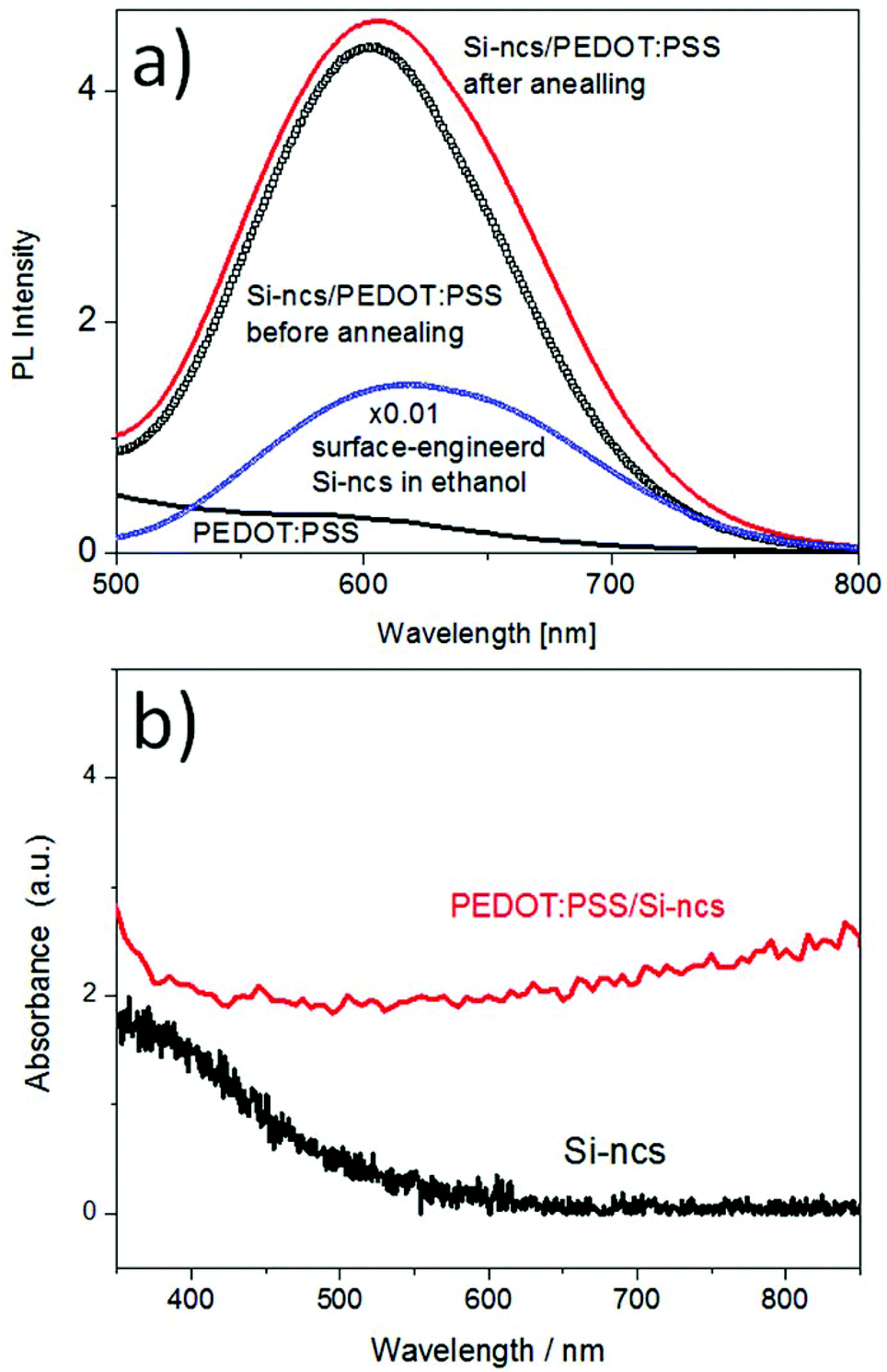 | ||
| Fig. 1 (a) Photoluminescence (PL) spectra for silicon nanocrystals (Si-ncs) after microplasma processing in ethanol (blue small squares) and Si-nc/PEDOT:PSS composites before (black large squares) and after annealing at 135 °C (red line). The PL of the PEDOT:PSS film without the Si-ncs after annealing at 135 °C is shown for comparison (black line). (b) Absorption spectra of the Si-nc/PEDOT:PSS composites after annealing at 135 °C (red line) and of the Si-ncs only (black line). | ||
The Si-nc/PEDOT:PSS nanocomposite is then used in organic solar cell devices. We have compared the performance of PTB7:[70]PCBM solar cells that used a PEDOT:PSS layer without Si-ncs with the performance of PTB7:[70]PCBM devices that used our new Si-nc/PEDOT:PSS nanocomposite (Fig. 2a). Here we expect the Si-ncs to absorb UV-photons and prevent their penetration into the PTB7:[70]PCBM active layer converting them into lower-wavelength photons. Fig. 2b shows typical current density versus voltage (J–V) characteristics under 100 mW cm−2 irradiance (1 sun). The device with the Si-nc/PEDOT:PSS nanocomposite exhibited a slight improvement in the fill factor (FF) from 68% to 71% and maintained the same open-circuit voltage (VOC) at 0.76 V. The short-circuit current density (JSC) was reduced from 14.26 mA cm−2 to 13.69 mA cm−2 representing a small change also reflected in negligible variations in the power conversion efficiency from 7.41% to 7.33%. The decrease in photocurrent generation may be in part due to a diminished carrier mobility in the PEDOT:PSS layer due to the presence of the Si-ncs. However, it is also likely that the presence of the Si-ncs is reducing light transmittance to the active layer in the 450–700 nm range; this is supported by the decrease of the external quantum efficiency (EQE) in the region from 450 nm to 700 nm (Fig. 2c). Nevertheless in the region where Si-nc absorption and down-conversion occur (below ∼400 nm) the EQE curve of the device with the nanocomposite (black dotted line in Fig. 2c) is higher than the EQE of the device with PEDOT:PSS only (red line in Fig. 2c).
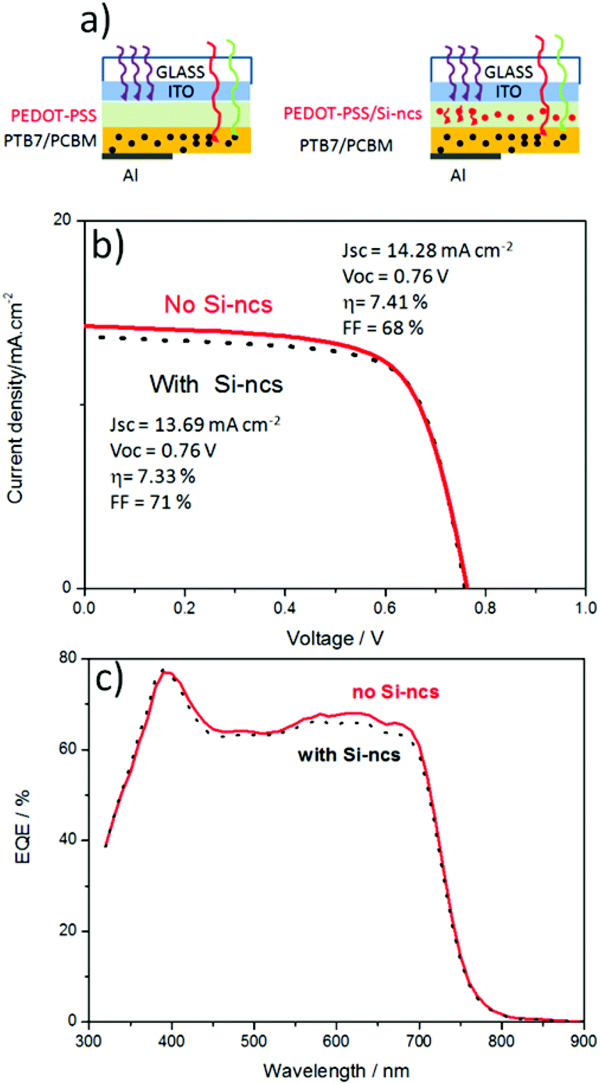 | ||
| Fig. 2 (a) Schematic device structure without (left) and with (right) the silicon nanocrystals (Si-ncs) in the PEDOT:PSS layer. (b) Current density versus voltage characteristics and (c) the corresponding external quantum efficiency (EQE) of solar cells with (black dotted line) and without (red full line) the Si-ncs in the PEDOT:PSS layer under 1 sun irradiance. | ||
Because a higher photon flux is expected to increase the Si-nc PL intensity,25 we would also expect an enhancement of the Si-nc contribution with concentrated sunlight radiation. Therefore, Fig. 3a compares the J–V characteristics with 100 mW cm−2 (1 sun), 200 mW cm−2 (2 suns) and 400 mW cm−2 (4 suns) irradiance for the solar cell without (full lines) and with the Si-ncs (dotted lines). The device performance parameters are also summarized in Table 1.
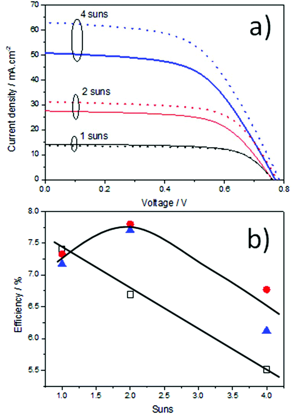 | ||
| Fig. 3 (a) Current density versus voltage (J–V) curves of PTB7:[70]PCBM solar cells with (full lines) and without (dotted lines) the Si-ncs in the PEDOT:PSS layer under irradiation at different levels of concentrated light; (b) conversion efficiencies of solar cell devices without (open symbols) and with the Si-ncs (full symbols); full red circles and full blue triangles refer to experiments repeated using the same device. | ||
| Suns | Organic solar cell devices | |||||||
|---|---|---|---|---|---|---|---|---|
| Without Si-ncs | With Si-ncs | |||||||
| V OC (V) | I SC (mA cm−2) | FF (%) | Efficiency (%) | V OC (V) | I SC (mA cm−2) | FF (%) | Efficiency (%) | |
| 1-sun | 0.76 | 14.28 | 68 | 7.41 | 0.76 | 13.69 | 71 | 7.33 |
| 2-suns | 0.77 | 27.57 | 63 | 6.69 | 0.78 | 31.13 | 65 | 7.80 |
| 4-suns | 0.77 | 50.69 | 56 | 5.51 | 0.78 | 62.92 | 55 | 6.77 |
The VOC remains essentially constant (less than 3% variation in all cases) as a function of irradiance. The two types of devices are also consistent in exhibiting a decreasing FF with increasing concentration (Table 1); because the open-circuit voltage is essentially invariant, increased carrier recombination at the PTB7:[70]PCBM interface cannot be responsible for reducing the FF.29 Most likely, the voltage across the series resistance increases due to higher current densities under concentrated sunlight and consequently affects negatively the FF. Importantly, a considerable and clear difference between the two types of devices, i.e. with and without Si-ncs, is observed for the JSC under increased irradiance. The 1-sun short-circuit current is slightly lower (by ∼4%) for the solar cell with the nanocomposite (13.69 mA cm−2) compared to the 1-sun JSC of the device without Si-ncs (14.28 mA cm−2). However, with concentrated light, the devices with Si-ncs exhibit much larger short-circuit current densities with respect to devices without Si-ncs: 31.13 mA cm−2vs. 27.57 mA cm−2 at 2-suns (∼13% increment) and 62.92 mA cm−2vs. 50.69 mA cm−2 at 4-suns (∼24% increment). In both types of devices, JSC increases linearly with the irradiance, however a much steeper gradient is observed for the cell with the Si-nc/PEDOT:PSS nanocomposite. The linear behavior is expected because the number of carriers is directly proportional to the number of photons absorbed.
Fig. 3b summarizes the conversion efficiency of solar cells without (open symbols) and with (full symbols) the Si-ncs in the PEDOT:PSS layer. The device without the Si-ncs showed a linear decreasing trend as the sunlight concentration was increased (Fig. 3b, open symbols); in contrast, the solar cells with the Si-nc/PEDOT:PSS nanocomposite exhibited a non-linear behavior with a maximum efficiency at about 2-suns (Fig. 3b, full symbols) for the results reported here and with an overall better performance under concentrated light; it is clear that the actual maximum efficiency may have occurred anywhere between 1-sun and 4-suns.
Organic devices under concentrated light are anticipated to exhibit higher current densities because the number of charge carriers generated is directly proportional to the number of photons absorbed. However, with concentrated light, the overall efficiency of organic devices is expected to decrease because intense light is detrimental to polymer transport properties. The devices without the Si-nc nanocomposite are therefore behaving as expected, i.e. the JSC increases linearly with solar concentration and the device efficiency decreases linearly. The non-linear behavior of the devices with the nanocomposite is evidence of a mechanism that is contributing to increasing device efficiency for >1-sun concentration and is eventually superseded by degrading polymer transport properties at 4-suns. We suggest that this mechanism can be identified with the down-conversion of the Si-ncs which essentially increases the lower wavelength photon flux to the active layer and increases the current density of the devices with Si-ncs (see Fig. 3a).
We will now also discuss the effect of the down-converting nanocomposite in hybrid solar cell devices. Hybrid devices are produced by also introducing 25 wt% Si-ncs into the active layer of the PTB7:[70]PCBM bulk-heterojunction. The device in this case is referred to as a hybrid organic/inorganic bulk-heterojunction because it includes an electronically active inorganic component (i.e. the Si-ncs). Therefore, in this case, we expect the Si-ncs to also affect the dissociation efficiency and transport properties of the device. It has been shown that the Si-ncs within conjugated polymers can act as acceptors with decent device efficiencies;5,19 however the Si-nc performance is still relatively poor, possibly due to a lower capacity of the Si-ncs to accept the electrons in comparison with [70]PCBM.
Fig. 4a shows the schematic structures of the devices without and with Si-ncs in the PEDOT:PSS layer; both hybrid devices of Fig. 4a include Si-ncs in the active layer, therefore, hereafter, we will use “with/without Si-ncs” only to refer to the presence of the Si-ncs in the PEDOT:PSS down-conversion layer. Fig. 4b compares the J–V characteristics of hybrid solar cells without and with Si-ncs in the PEDOT:PSS layer under 1-sun irradiation and Fig. 4c reports on the corresponding EQE characteristics. The inset of Fig. 4c shows the energy band diagram of the device.
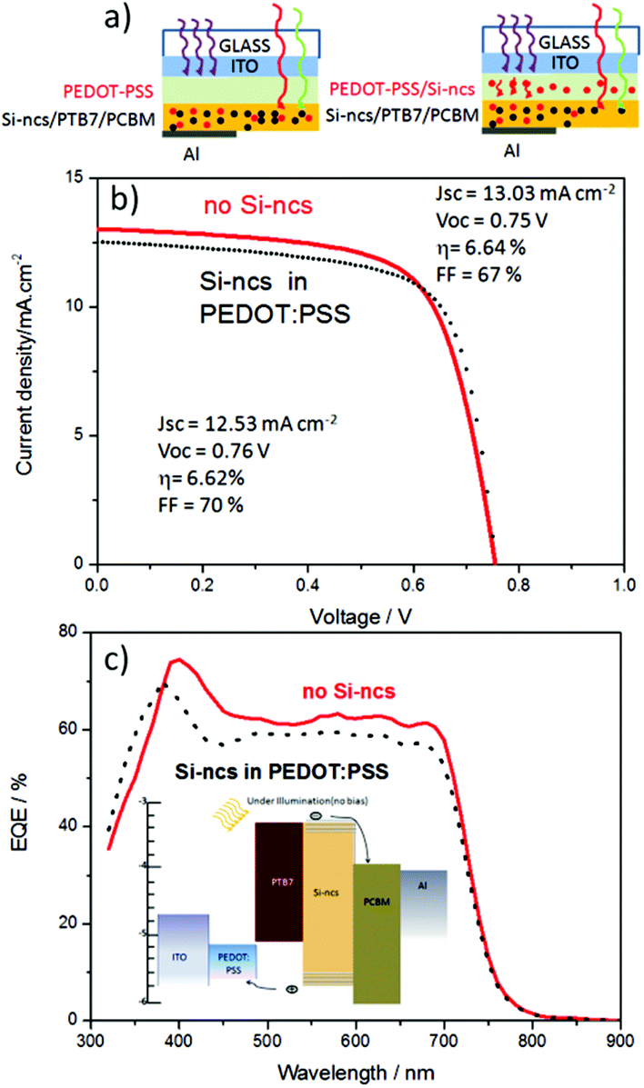 | ||
| Fig. 4 (a) Schematic structure of hybrid devices without (left) and with (right) the silicon nanocrystals (Si-ncs) in the PEDOT:PSS layer. (b) Current density versus voltage (J–V) curves of solar cells without and with the Si-nc/PEDOT:PSS nanocomposite under 1-sun irradiation. (c) The corresponding external quantum efficiencies of the device without and with the Si-ncs in the PEDOT:PSS layer; the inset shows the energy band diagram of the device architecture. | ||
The performance of the solar cell with the Si-ncs introduces identical effects into the hybrid device architecture as observed for fully-organic devices (compare Fig. 4b with 2b and 4c with 2c). The Si-ncs in the PEDOT:PSS layer do not visibly influence the overall conversion efficiency (∼6.6%) in hybrid devices (Fig. 4b), exhibiting a slight improvement in the FF, maintaining about the same VOC and reducing slightly the short-circuit current density. Similar to the organic devices (Fig. 2), the decrease in photocurrent may be due to a diminished carrier mobility in the PEDOT:PSS layer and due to the reduced light transmittance to the active layer in the 450–700 nm range; the latter is also in this case supported by the decrease of the EQE in the region from 450 nm to 700 nm (Fig. 4c). Furthermore, the increased EQE in the region where the Si-nc absorption and down-conversion is expected to occur (below ∼410 nm) is also confirmed; see black dotted line in Fig. 4c for the devices with the Si-ncs vs. the red line for the devices without the Si-ncs.
Furthermore, the same trends are observed when hybrid devices with/without Si-ncs in the PEDOT:PSS layer are studied under concentrated light. Fig. 5a presents current density versus voltage curves of hybrid solar cells with (dotted lines) or without (full lines) the Si-ncs in the PEDOT:PSS layer under 100 mW cm−2, 200 mW cm−2 and 400 mW cm−2 irradiance. Fig. 5 can be directly compared with Fig. 3, which reports on the corresponding devices with a fully organic active layer. The device performance parameters of Fig. 5 are also summarized in Table 2.
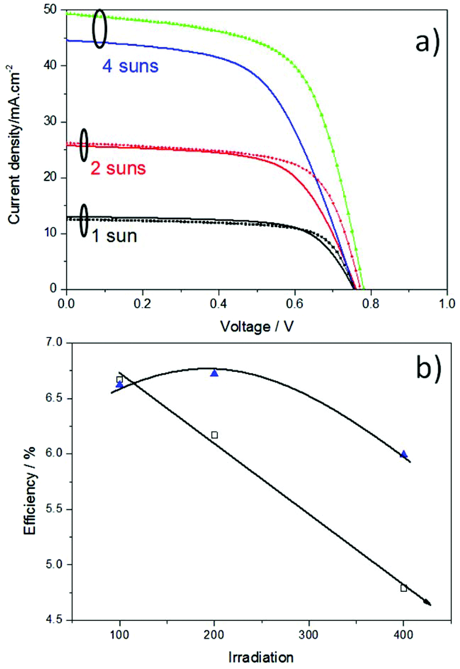 | ||
| Fig. 5 (a) Current density versus voltage curves of solar cells with 25 wt% silicon nanocrystals (Si-ncs) in the PTB7:[70]PCBM active layer with (dotted lines) and without (full lines) the Si-ncs in the PEDOT:PSS layer under 1-, 2-, and 4-sun irradiation. (b) The corresponding conversion efficiency of devices without (open symbols) and with the Si-ncs (full symbols) in the PEDOT:PSS layer. | ||
| Suns | Hybrid solar cell devices | |||||||
|---|---|---|---|---|---|---|---|---|
| Without Si-ncs | With Si-ncs | |||||||
| V OC (V) | I SC (mA cm−2) | FF (%) | Efficiency (%) | V OC (V) | I SC (mA cm−2) | FF (%) | Efficiency (%) | |
| 1-sun | 0.75 | 13.03 | 67 | 6.64 | 0.76 | 12.53 | 70 | 6.62 |
| 2-suns | 0.76 | 25.76 | 63 | 6.17 | 0.77 | 26.21 | 66 | 6.72 |
| 4-suns | 0.76 | 44.61 | 57 | 4.79 | 0.78 | 49.36 | 62 | 5.99 |
Under concentrated light, in all cases, the introduction of Si-ncs into the PEDOT:PSS layer (dotted lines in both Fig. 3 and 5) is beneficial for the overall performance of the solar cell. Since under concentrated light Si-ncs clearly show nonlinear PL properties,30 it is reasonable and highly likely that the device improvements originate from the down-conversion of high energy photons into red-photons.11,31 The nanocomposite also slightly improves the VOC to 0.78 V in both organic and hybrid devices and the efficiency of the non-linear behavior of organic devices (Fig. 3b) due to the Si-nc/PEDOT:PSS layer is again observed for hybrid solar cells (Fig. 5b). In summary, the results from 15 devices are reported here for the same Si-nc/PEDOT:PSS nanocomposite material providing a consistent picture of its performance. These results also strongly support the repeatability and reliability of the Si-nc/PEDOT:PSS nanocomposite layer under different conditions and within a range of different devices.
The effectiveness of the down-conversion results from the balance between absorption of the Si-ncs at the lower wavelengths and the quantum yield (QY) of the Si-ncs that determine the re-emission at a more favorable wavelength range. The contribution of the down-conversion mechanism can be inferred from the QY of the Si-ncs. The initial QY of our Si-ncs is ∼10%, which can be increased to ∼30% with surface engineering by microplasma (see the ESI†); we can therefore assume that the efficiency of down-conversion could be readily obtained at this figure considering the isotropic nature of the PL. Also, it has to be noted that the initial 10% is relatively modest and that QY above 80% could be achieved using optimized Si-ncs produced for instance by plasmas.32,33 Therefore it is clear that the down conversion effect and efficiency improvement could be dramatically higher and in particular efficiency improvements could be achieved even at 1-sun, without concentration. Since down conversion can be in principle tuned by Si-nc size and the concentration, another advantage of embedding Si-nc/PEDOT:PSS nanocomposites could be the integration with tandem solar cells whereby easier matching of photocurrents of the top with the bottom cell can be more easily achieved.34
Although the effect of the Si-ncs in the active layer is not the main focus of this work, it may be important to highlight some important aspects of the Si-ncs’ direct contribution to carrier generation and transport. This can be done by comparing the results that relate to the devices without the Si-ncs in the down-conversion PEDOT:PSS layer, i.e. the red curves of Fig. 2b and c with the red curves of Fig. 4b and c and the corresponding performance parameters (i.e. the italicized values in Tables 1 and 2). The VOC and FF are not affected by the introduction of Si-ncs into the active layer, however the current density is visibly reduced, which is the main cause of lower efficiencies for devices with the Si-ncs in the active layer. A range of factors may have contributed to the decrease of the device performance. The Si-ncs necessarily prevent the organic interface from functioning as in standard organic solar cells, degrading its performance due to both a reduced absorption (note that polymer absorption is ∼10 higher than Si-ncs) as well as a compromised organic junction. At the same time, under the conditions of Fig. 4 and 5, the benefits of the Si-nc layer may be still limited so that overall, the device with the Si-ncs has suffered in terms of performance. The unaffected VOC and FF support this argument and may suggest that an optimized concentration of the Si-ncs in the active layer may lead to a beneficial contribution of the Si-ncs. More specifically, the FF confirms that the architecture with Si-ncs in the active layer is not morphologically affected. Furthermore, the VOC behavior in Fig. 5b suggests that the Si-ncs in the active layer are not negatively affecting dissociation efficiency and in light of the reduced absorption may instead contribute to it. It is possible that the Si-ncs’ higher density of states provide dissociation sites for excitons created in the polymer heterojunction and/or contribute to change favorably the alignment between energy levels. The Si-nc concentration needs therefore to be optimized to preserve these beneficial effects vs. the reduced absorption. Finally, it may be important to highlight that the presence of the Si-ncs in the active layer may have enhanced the down-conversion mechanism. This can be observed by comparing Fig. 2c and 4c in the range below 410 nm. The enhancement of the EQE due to Si-ncs in the PEDOT:PSS layer is much more pronounced when the Si-ncs are also in the active layer (see the “Si-ncs in PEDOT:PSS” black dotted line vs. the “no Si-ncs” red line in Fig. 4c) compared to the fully-organic devices without the Si-ncs in the active layer (see the “with Si-ncs” black dotted line vs. the “no Si-ncs” red line in Fig. 2c).
4. Conclusions
We have demonstrated the possibility of easily introducing Si-ncs into organic device architectures with different contributions to the solar cell performance. Surface-engineered Si-ncs using microplasma offer excellent opportunities for optimized interactions with polymers derived from easily processed colloids in water and other solvents (e.g. chlorobenzene). The Si-nc water-based nanocomposite has resulted in an important contribution to the device efficiency when used as an optical down-converter with enhanced photocurrent generation. With concentrated light (<10-suns), the use of photoluminescent surface-engineered Si-ncs introduces advantages to organic and hybrid devices whereby both efficiency and durability can be improved. Importantly, it is also confirmed that the nanocomposite-induced down-conversion performs better at increased but still relatively low light intensity (<2-suns), which represents an important range of radiation intensity largely determined by geographical location and weather conditions. When Si-ncs were integrated into the active layer the overall device performance suffered from reduced absorption. However, the VOC and FF are in support of a positive contribution and most importantly, the presence of the Si-ncs in the active layer enhances the down-conversion effect of the Si-ncs. Therefore, tuning the concentration of Si-ncs in both the PEDOT:PSS as well as in the active layer represents an opportunity to increase/decrease the EQE in different parts of the spectrum and to tailor the conversion efficiency.Acknowledgements
This work was partially supported by a NEDO project, the Royal Society International Exchange Scheme (IE120884), the Leverhulme International Network (IN-2012-136) and EPSRC (EP/K022237/1). DM also acknowledges the support of the JSPS Bridge Fellowship and SM acknowledges the financial support of the University of Ulster Vice-Chancellor Studentship.Notes and references
- X. D. Pi, R. W. Liptak, J. Deneen Nowak, N. P. Wells, C. B. Carter, S. A. Campbell and U. Kortshagen, Air-Stable Full- Visible-Spectrum Emission from Silicon Nanocrystals Synthesized by an All-Gas-Phase Plasma Approach, Nanotechnology, 2008, 19, 245603–245609 CrossRef CAS PubMed.
- L. Pavesi, L. Dal Negro, C. Mazzoleni, G. Franzò and F. Priolo, Optical gain in silicon nanocrystals, Nature, 2000, 408, 440–444 CrossRef CAS PubMed.
- D. Kovalev and M. Fujii, Silicon Nanocrystals: Photosensitizers for Oxygen Molecules, Adv. Mater., 2005, 17, 2531–2544 CrossRef CAS PubMed.
- D. Timmerman, I. Izeddin, P. Stallinga, I. N. Yassevich and T. Gregorkiewicz, Space-separated quantum cutting with Si nanocrystals for photovoltaic applications, Nat. Photonics, 2008, 2, 105–109 CrossRef CAS PubMed.
- C.-Y. Liu, Z. C. Holman and U. R. Kortshagen, Optimization of Si NC/P3HT Hybrid Solar Cells, Adv. Funct. Mater., 2010, 20, 2157–2164 CrossRef CAS PubMed.
- F. Hua, M. T. Swihart and E. Ruckenstein, Efficient Surface Grafting of Luminescent Silicon Quantum Dots by Photoinitiated Hydrosilylation, Langmuir, 2005, 21, 6054–6062 CrossRef CAS PubMed.
- A. J. Nozik, Nanoscience and Nanostructures for Photovoltaics and Solar Fuels, Nano Lett., 2010, 10, 2735–2742 CrossRef CAS PubMed.
- V. Sark, M. Meijerink, R. E. I. Schropp, J. A. M. Van Roosmalen and E. H. Lysen, Enhancing solar cell efficiency by using spectral converters, Sol. Energy Mater. Sol. Cells, 2005, 87, 395–409 CrossRef PubMed.
- N. Grossiord, J. M. Kroon, R. Andriessen and P. W. M. Blom, Degradation mechanisms in organic photovoltaic devices, Org. Electron., 2012, 13, 432–456 CrossRef CAS PubMed.
- F. Sgrignuoli, P. Ingenhoven, G. Pucker, V. D. Mihailetchi, E. Froner, Y. Jestin, E. Moser, G. Sànchez and L. Pavesi, Purcell effect and luminescent downshifting in silicon nanocrystals coated back-contact solar cells, Sol. Energy Mater. Sol. Cells, 2015, 132, 267–274 CrossRef CAS PubMed.
- V. Švrcek, A. Slaoui and J.-C. Muller, Silicon nanocrystals as light converter for solar cells, Thin Solid Films, 2004, 451, 384–391 CrossRef PubMed.
- V. Švrcek, T. Yamanari, D. Mariotti, S. Mitra, K. Matsubara and M. Kondo, Enhancement of Polymer Solar Cell Performance under Low-Concentrated Sunlight by 3D Surface-engineered Silicon Nanocrystals, 39th IEEE Photovoltaic Specialists Conference, Tampa Florida, June 2013, Proc. on CD A1-911 (1-5) , A0-911, 1-5 Search PubMed.
- H. Cotal, Ch. Fetzer, J. Boisvert, G. Kinsey, R. King, P. Hebert, H. Yoon and N. Karam, III–V multijunction solar cells for concentrating photovoltaics, Energy Environ. Sci., 2009, 2, 174–192 CAS.
- E. P. Yao, C. S. Ho, C. Yu, E. L. Huang, Y. N. Lai and W. C. H. An, Alternative Approach for Improving Performance of Organic Photovoltaics by Light-Enhanced Annealing, Int. J. Photoenergy, 2014, 120693 Search PubMed.
- J. S. Batchelder, A. H. Zewail and T. Cole, Luminescent solar concentrators. Experimental and theoretical analysis of their possible efficiencies, Appl. Opt., 1981, 20, 3733–3740 CrossRef CAS PubMed.
- M. J. Currie, K. Jonathan, J. K. Mapel, T. D. Heidel, S. Goffri and M. A. Baldo, High-Efficiency Organic Solar Concentrators for Photovoltaics, Science, 2008, 321, 226–230 CrossRef CAS PubMed.
- D. Mariotti, S. Mitra and V. Švrcek, Surface-engineered silicon nanocrystals, Nanoscale, 2013, 5(4), 1385–1398 RSC.
- V. Švrcek, D. Mariotti and M. Kondo, Microplasma-induced surface engineering of silicon nanocrystals in colloidal dispersion, Appl. Phys. Lett., 2010, 97(1–3), 161502 CrossRef PubMed.
- V. Švrcek, T. Yamanari, D. Mariotti, K. Matsubara and M. Kondo, Enhancement of hybrid solar cell performance by polythieno [3,4-b]thiophenebenzodithiophene and microplasma-induced surface engineering of silicon nanocrystals, Appl. Phys. Lett., 2012, 100, 223904 CrossRef PubMed.
- S. Mitra, V. Švrček, D. Mariotti, K. Matsubara and M. Kondo, Microplasma-induced liquid chemistry as a tool for stabilization of silicon nanocrystals optical properties in water, Plasma Processes Polym., 2014, 11, 158–163 CrossRef CAS PubMed.
- L. Pavesi and R. Turan, Silicon nanocrystals: fundamentals, synthesis and applications, Wiley-VCH Verlag GmbH & Co. KGaA, 2010 Search PubMed.
- M. Wolkin, J. Jorne, P. Fauchet, G. Allan and C. Delerue, Electronic States and Luminescence in Porous Silicon Quantum Dots: The Role of Oxygen, Phys. Rev. Lett., 1999, 82, 197–200 CrossRef CAS.
- Y. H. Ogata, N. Yoshimi, R. Yasuda, T. Tsuboi, T. Sakka and A. Otsuki, Structural Change in P-type Porous Silicon by Thermal Annealing, J. Appl. Phys., 2001, 90, 6487–6492 CrossRef CAS PubMed.
- H. Kim, J. Lee, S. Ok and Y. Choe, Effects of pentacene-doped PEDOT:PSS as a hole-conducting layer on the performance characteristics of polymer photovoltaic cells, Nanoscale Res. Lett., 2012, 7(1), 5–11 CrossRef PubMed.
- Y. Liu, T. P. Chen, C. Y. Ng, L. Ding, S. Zhang, Y. Q. Fu and S. Fung, Depth profiling of charging effect of Si nanocrystals embedded in SiO2: a study of charge diffusion among Si nanocrystals, J. Phys. Chem. B, 2006, 110, 16499–16502 CrossRef CAS PubMed.
- S. Mitra, S. Cook, V. Švrček, R. A. Blackley, Z. Wuzong, J. Kovač, U. Cvelbar and D. Mariotti, Improved optoelectronic properties of silicon nanocrystals/polymer nanocomposites by microplasma-induced liquid chemistry, J. Phys. Chem. C, 2013, 117, 23198–23202 CAS.
- V. Svrcek, K. Dohnalova, D. Mariotti, M. T. Trinh, R. Limpens, S. Mitra, T. Gregorkiewicz, K. Matsubara and M. Kondo, Dramatic Enhancement of Photoluminescence Quantum Yields for Surface-Engineered Si Nanocrystals within the Solar Spectrum, Adv. Funct. Mater., 2013, 23, 6051–6058 CrossRef CAS PubMed.
- D. Alemu, H.-Y. Wei, K.-Ch. Ho and Ch.-W. Chu, Highly conductive PEDOT:PSS electrode by simple film treatment withmethanol for ITO-free polymer solar cells, Energy Environ. Sci., 2012, 5, 662–669 Search PubMed.
- K. W. Kemp, A. J. Labelle, S. M. Thon, A. H. Ip, I. J. Kramer, S. Hoogland and E. H. Sargent, Interface Recombination in Depleted Heterojunction, Photovoltaics based on Colloidal Quantum Dots, Adv. Energy Mater., 2013, 3, 917–921 CrossRef CAS PubMed.
- K. Luterová, K. Dohnalová, V. Švrcek, I. Pelant, J. P. Likforman, O. Cregut, P. Gilliot and B. Honerlage, Optical gain in porous silicon grains embedded in sol-gel derived SiO2 matrix under femtosecond excitation, Appl. Phys. Lett., 2004, 84, 3280 CrossRef PubMed.
- C. Y. Huang, D. Y. Wang, C. H. Wang, Y. T. Chen, Y. T. Wang, Y. T. Jiang, Y. J. Yang, C. C. Chen and Y. F. Chen, Efficient Light Harvesting by Photon Downconversion and Light Trapping in Hybrid ZnS Nanoparticles/Si Nanotips Solar Cells, ACS Nano, 2010, 4(10), 5849–5854 CrossRef CAS PubMed.
- J. B. Miller, A. R. Van Sickle, R. j. Anthony, D. M. Kroll, U. R. Kortshagen and E. K. Hobbie, Ensemble brightening and enhanced quantum yield in size-purified silicon nanocrystals, ACS Nano, 2012, 6(8), 7389–7396 CrossRef CAS PubMed.
- S. Askari, I. Levchenko, K. Ostrikov, P. Maguire and D. Mariotti, Crystalline Si nanoparticles below crystallization threshold: Effects of collisional heating in non-thermal atmospheric-pressure microplasmas, Appl. Phys. Lett., 2014, 104, 163103 CrossRef PubMed.
- C. Kerestes, Y. Wang, K. Shreve, J. Mutitu, T. Creazzo, P. Murcia and A. Barnett, Design, fabrication, and analysis of transparent silicon solar cells for multi-junction assemblies, Prog. Photovoltaics, 2013, 21, 578–587 CAS.
Footnote |
| † Electronic supplementary information (ESI) available. See DOI: 10.1039/c5nr02703a |
| This journal is © The Royal Society of Chemistry 2015 |