
 Open Access Article
 This Open Access Article is licensed under a Creative Commons Attribution-Non Commercial 3.0 Unported Licence
Design, fabrication and charge recombination analysis of an interdigitated heterojunction nanomorphology in P3HT/PC70BM solar cells†
Victor S.
Balderrama
ab,
Josep
Albero
c,
Pedro
Granero
a,
Josep
Ferré-Borrull
a,
Josep
Pallarés
a,
Emilio
Palomares
de and
Lluis F.
Marsal
*a
aUniversity of Rovira i Virgili, Països Catalans 26, 43007 Tarragona, Spain. E-mail: lluis.marsal@urv.cat
bSección de Electrónica del Estado Sólido, Departamento de Ingeniería Eléctrica, CINVESTAV, Av. IPN No. 2508, 07360, D.F., Mexico
cInstitute of Chemical Technology of Valencia (ITQ), Avenue De los Naranjos s/n, 46022 Valencia, Spain
dInstitute of Chemical Research of Catalonia (ICIQ) Països Catalans 24, 43007 Tarragona, Spain
eICREA. Passeig Lluís Companys, 23, 08010 Barcelona, Spain
First published on 15th June 2015
Abstract
In this work interdigitated heterojunction photovoltaic devices were manufactured. A donor layer of P3HT nanopillars was fabricated by soft nanoimprinting using nanoporous anodic alumina templates. Subsequently, the PC70BM acceptor layer was deposited by spin coating on top of the P3HT nanopillars using a solvent that would not dissolve any of the previous material. Anisole solvent was used because it does not dissolve the bottom donor layer of nanopillars and provides a good wettability between the two materials. Charge extraction was used to determine the charge carrier densities n on the interdigitated heterojunction under operating conditions. Moreover, transient photovoltage measurements were used to find the recombination rate constant in combination with the charge carrier density. At the same time, the interdigitated structure was also compared with bulk heterojunction and bilayer solar cells manufactured with the same polymeric and fullerene materials in order to understand the recombination loss mechanisms in the ordered and disordered nanomorphologies of the active layers.
1. Introduction
In recent years, intense effort has been put into developing organic solar cells (OSCs) that are at least as cost effective as the market-dominant silicon solar cells. The advantages of their low cost, light-weight, large area, flexibility and ease of processing make organic materials an attractive target.1–3 The power conversion efficiency of photovoltaic devices has been improved by designing and synthesizing new materials with low band-gaps, changing the structure of devices,3,4 controlling the nanoscale morphology with additives, applying thermal or solvent annealing, controlling evaporation with solvents5,6 to increase the interfacial area between donor and acceptor,7 and making nanostructure morphologies such as nanogratings, nanopillars, nanorods and nanodots.4,8–12In order to improve the performance parameters, nanostructured morphologies have been fabricated with a standard configuration layered with poly-(3-hexylthiophene) (P3HT)/[6,6]-phenyl-C61-butyric acid methyl ester (PCBM), with power conversion efficiencies reported between 1.1–3.25%.10,11,13–17
It is well known that the power conversion efficiency is limited, among other factors, by the diffusion length of excitons in the photoactive layer after they have been generated (typically this length is in the range of tens of nanometers in most organic semiconductors).18–20 To prevent the loss of the excitons before dissociation, it is necessary to have a well defined morphology for the interfaces between the polymer-fullerene materials, with equal distances of diffusion lengths. The free electrons and holes after the exciton dissociation are transported by their corresponding material and collected at the metal electrodes. This morphology is known as a bulk heterojunction.21–23
One promising way to increase the power conversion efficiency of polymer photovoltaic cells is to fabricate a well-controlled and ordered interdigitated heterojunction nanomorphology (IHJN) by soft nanoimprinting. The excitons generated inside of this nanomorphology can move at the interface to dissociate into electrons and holes and nearly all of the free charge carriers can travel along the uninterrupted pathway of the material until they reach their respective electrodes. The vertical IHJN allows the domains in the p-type donor material and the n-type acceptor material to be aligned normal to the electrode surfaces, thus increasing their crystallinity and charge carrier mobility and reducing the recombination rates inside the device.19,24,25 The main progresses in IHJNs have been achieved by new fabrication techniques and technologies. The interdigitated nanostructures can be manufactured by nanoimprinting lithography (NIL),26 solvent-assisted nanoimprinting lithography (SANIL),11 electron-beam lithography (EBL),17 spin-coating and nanoimprinting with template-based methods,13,16,27 among many others.4,8,28–32
Here we report the use of a nanoimprinting method, in which nanoporous anodic alumina templates (NAATs) are used to fabricate interdigitated nanostructures in a cost effective and straightforward fashion.27 NAATs are widely used as a template material because they are porous, have a good hexagonal order and the geometric characteristics can be easily controlled.33–35 NAATs and soft nanoimprinting can be combined to provide the vertical nanostructured polymer and the temperature, pressure, and time of the imprint can be precisely controlled.15,28,36 In order to get the complete IHJN structure for an OSC application, we used a combination of spin coating and soft nanoimprinting by NAATs to obtain conformal thin films of nanopillars (NP) as the donor layers, which made it possible to fabricate several P3HT/PC70BM solar cell devices after the P3HT-NPs had been infiltrated with PC70BM. An anisole (C7H8O) solvent was used to dissolve the fullerene without destroying the donor layer. Bulk heterojunction (BHJ) and bilayer (BL) organic solar cells were fabricated for the purpose of comparison with interdigitated solar cells. The fabrication process and conditions were very similar to those of the interdigitated cells.
Once the photovoltaic devices with the IHJNs had been obtained, we needed to understand the physical processes involved in the device operation. The typical electrical characterization, as current–voltage (J–V), is not enough to understand the solar cell limitations. Some key parameters for better understanding the factors that limit the power conversion efficiency are the charge density distribution and the charge recombination dynamics.
Herein, we apply charge extraction (CE) and transient photovoltage (TPV) measurements to the IHJN solar cells under steady state operating conditions with the aim of analyzing and determining the charge densities, the carrier recombination dynamics and the carrier lifetime dependency on voltage. These measurements are often used in research on BHJ solar cells37–39 and dye-sensitized solar cells,40 but have not been previously applied to interdigitated structures. Indeed, all the results obtained from the optoelectronic techniques used in this study (CE and TPV) reveal that its interdigitated device nanomorphology is a determining geometric factor that directly affects the charge carrier density, recombination losses and FF during device operation.
2. Experimental section
2.1 Materials
ITO-coated glass substrates (with a nominal sheet resistance of 15 ohm per square and a thickness of 120 nm) were purchased from PsiOTec Ltd. PEDOT:PSS FHC was acquired from Ossila Ltd, P3HT (melting point 238 °C, Mw = 17![[thin space (1/6-em)]](https://www.rsc.org/images/entities/char_2009.gif) 500 g mol−1, 99.995% regio-regularity) and PC70BM (Mw = 1031.0 g mol−1) were purchased from Sigma-Aldrich and Solenne BV, respectively. High-purity (99.99%) silver wire was obtained from Testbourne Ltd, and calcium pellets with high-purity (99.99%) were purchased from Kurt J. Lesker.
500 g mol−1, 99.995% regio-regularity) and PC70BM (Mw = 1031.0 g mol−1) were purchased from Sigma-Aldrich and Solenne BV, respectively. High-purity (99.99%) silver wire was obtained from Testbourne Ltd, and calcium pellets with high-purity (99.99%) were purchased from Kurt J. Lesker.
2.2 Fabrication of NAAT
The NAAT samples were fabricated by a two-step anodization process. Before anodizing, the aluminium (Al) substrates were electropolished in a mixture of ethanol (EtOH) and perchloric acid (HClO4) 4:1 (v:v) at 20 V for 3 min. After this, the first anodization step was performed in an aqueous solution of oxalic acid (H2C2O4) 0.3 M at 40 V and 5 °C for 24 h. Subsequently, the alumina film was selectively dissolved by wet chemical etching in a mixture of phosphoric acid (H3PO4) 0.4 M and chromic acid (H2CrO7) 0.2 M at 70 °C. Then, the second anodization step was conducted under the same anodization conditions as the first step. The anodization time during this step was adjusted to 60 seconds in order to modify the pore length. Finally, the pore diameter was enlarged by a wet chemical etching procedure in an aqueous solution of H3PO4 5 wt%. Subsequently, the NAATs were modified by DPMS (DMS-T22) to reduce the surface energy of the templates, the reaction mechanism of which was explained previously by Krumpfer and co-authors.55 The NAATs were immersed in DPMS at 120 °C for 24 h, and then rinsed with toluene, followed by acetone, ethanol, and DI water. Finally the substrates were dried with nitrogen.
2.3 Device fabrication
Photovoltaic IHJN-OSC devices were fabricated on pre-cleaned patterned ITO glass substrates. 40 nm of PEDOT:PSS was applied to the substrates by spin coating at 3500 rpm for 45 s. The PEDOT:PSS films were annealed at 110 °C for 20 min. The P3HT solution was prepared in chlorobenzene (C6H5Cl) and it was then spin-coated onto the PEDOT:PSS/ITO glass under nitrogen to obtain a thin film of P3HT. Afterwards, the nanoimprinting was optimized and carried out with the NAATs by applying 2 MPa at 60 °C for 5 min to the previous fabricated P3HT layer to get the P3HT-NP. The PC70BM solution was prepared in anisole solvent (C7H8O) at 10 mg ml−1 and it was deposited on top of the P3HT-NP by spin coating at 3000 rpm to backfill the spaces between the nanopillar arrays and to form a continuous PC70BM thin film on top. This process was conducted as rapidly as possible to avoid any possible interfacial mixing.BHJ-OSCs and planar bilayer (BL)-OSCs were manufactured for the purpose of comparison with the IHJN-OSCs. The BL-OSCs were fabricated under the same conditions as the IHJN-OSCs, but without the nanoimprinting process.
The BHJ-OSCs were manufactured using the same ITO substrates and PEDOT:PSS layer as for the IHJNs. A blend of P3HT:PC70BM (ratio 1:1) was prepared in chlorobenzene (CB) solution and then stirred for 18 h at 40 °C. The active layer was deposited by spin coating at 600 rpm for 45 s. Afterwards, all the structures (i.e. IHJN-OSC, BHJ-OSC and BL-OSC) were deposited on the metal contact by evaporation through a shadow to give devices with an active area of 0.09 cm2. Ca (20 nm) and Ag (100 nm) were deposited at a rate of 0.15 Å s−1 and 0.5–0.8 Å s−1 respectively. Then, post-processing annealing was carried out by heating at 130 °C for 20 min.
2.4 NAAT structure characterization
The NAAT samples and IHJN-OSC, BHJ-OSC and BL-OSC structures were characterized by environmental scanning electron microscopy (ESEM FEI Quanta 600). The standard image processing package (ImageJ, a public domain program developed at the RSB of the NIH, USA) was used to carry out the ESEM image analysis. Photoluminescence (PL) was measured in a fluorescence spectrophotometer from Photon Technology International Inc. for the three kinds of structures. A Xe lamp was used as the excitation light source at room temperature with an excitation wavelength (λex) of 510 nm and the emission spectra were recorded at an angle of 20°. The absorption spectra were measured for the three sets of IHJN, BHJ and BL structures at room temperature with a Perkin Elmer Lambda 950 UV/VIS/NIR spectrometer. Atomic force microscopy (AFM Agilent 6400) was used to make several characterizations of the surface morphology of the IHJN, BHJ and BL layer structures in the tapping mode.2.5 Device testing
The J–V characteristics of the devices were measured at room temperature using a Keithley 2400 source measurement unit in combination with a solar simulator (Abet Technologies model 11000 class type A, Xenon arc) automatically controlled with a computer. Appropriate filters were used to reproduce the AM 1.5 G spectrum. A light intensity of 100 mW cm−2 was applied to test the organic solar cell devices under illumination. The light intensity was calibrated with an NREL certified monocrystalline silicon photodiode. Film thicknesses were measured by a Dektak 150 surface profilometer. In addition, J–V dark curves were recorded for all of the photovoltaic devices.CE was used to determine the distribution of the charge carrier density (n) in the devices under different light and voltage conditions. The general CE procedure is to leave the device in an open circuit condition while illuminating at different intensities. Then, the device is shorted while simultaneously turning off the light, and the resulting discharging current transient through a small external load resistor is measured. The desired illumination intensity is achieved with a white light LED ring from LUXEON® Lumileds connected to a DC power supply and a TGP110 function generator that allows the LEDs to reach a background illumination up to 1 sun on the ITO side of the device. The LEDs were typically turned on for approximately 100 ms so that they could reach steady state conditions. The LEDs have a rise/fall time of <100 ns. After the light is switched off and the circuit is temporally closed, the charges are forced to pass through a TDS 2022 oscilloscope from Tektronix© that records the drop in voltage across a resistance of 50 Ω.
In the TPV measurements, the devices were connected to the 1 MΩ input terminal of a Tektronix© TDS2022 oscilloscope and the background illumination was obtained from a ring of 6 white LEDs from LUXEON®. The small perturbation (5 mV) was applied through a light pulse (N2 laser nominal wavelength, 50 ns pulses). The charge recombination rate was calculated for illumination intensities ranging from 0.1 sun to 1 sun.
3. Results and discussion
The preparation of the NAATs was carried out by the two-step anodization process that was described in the Experimental section.33,34 The pore length was controlled by the anodization time and the pore diameter was enlarged by a wet chemical etching procedure after anodization. The pore diameter (ϕp), pore length (Hp) and interpore distance (dint) were 60 ± 4 nm, 80 ± 5 nm and 100 ± 4 nm, respectively. A total of twenty NAAT samples were manufactured and analyzed. The fabrication conditions of the NAAT samples are summarized in Table S1 and shown in Fig. S1 of the ESI.† The NAATs were modified by dimethylpolysiloxane (DPMS) to reduce the surface energy of the templates as described in the Experimental section. The results showed that they became more hydrophobic, as was reported previously.16 Fig. S2(a)–(c) (ESI†) show the top-view, tilt-view and cross section-view provided by environmental scanning electron microscopy (ESEM) images of the NAATs after fabrication with an oxalic acid electrolyte (H2Cr2O7).Fig. 1(a–g) shows the preparation of an IHJN-OSC based on a P3HT-NP array. The fabrication process of the IHJN-OSC first required P3HT to be deposited on the structures prepared from poly-(ethylene dioxythiophene) doped with poly-(styrene sulphonic acid) (PEDOT:PSS)/indium tin oxide (ITO), as shown in Fig. 1(a).
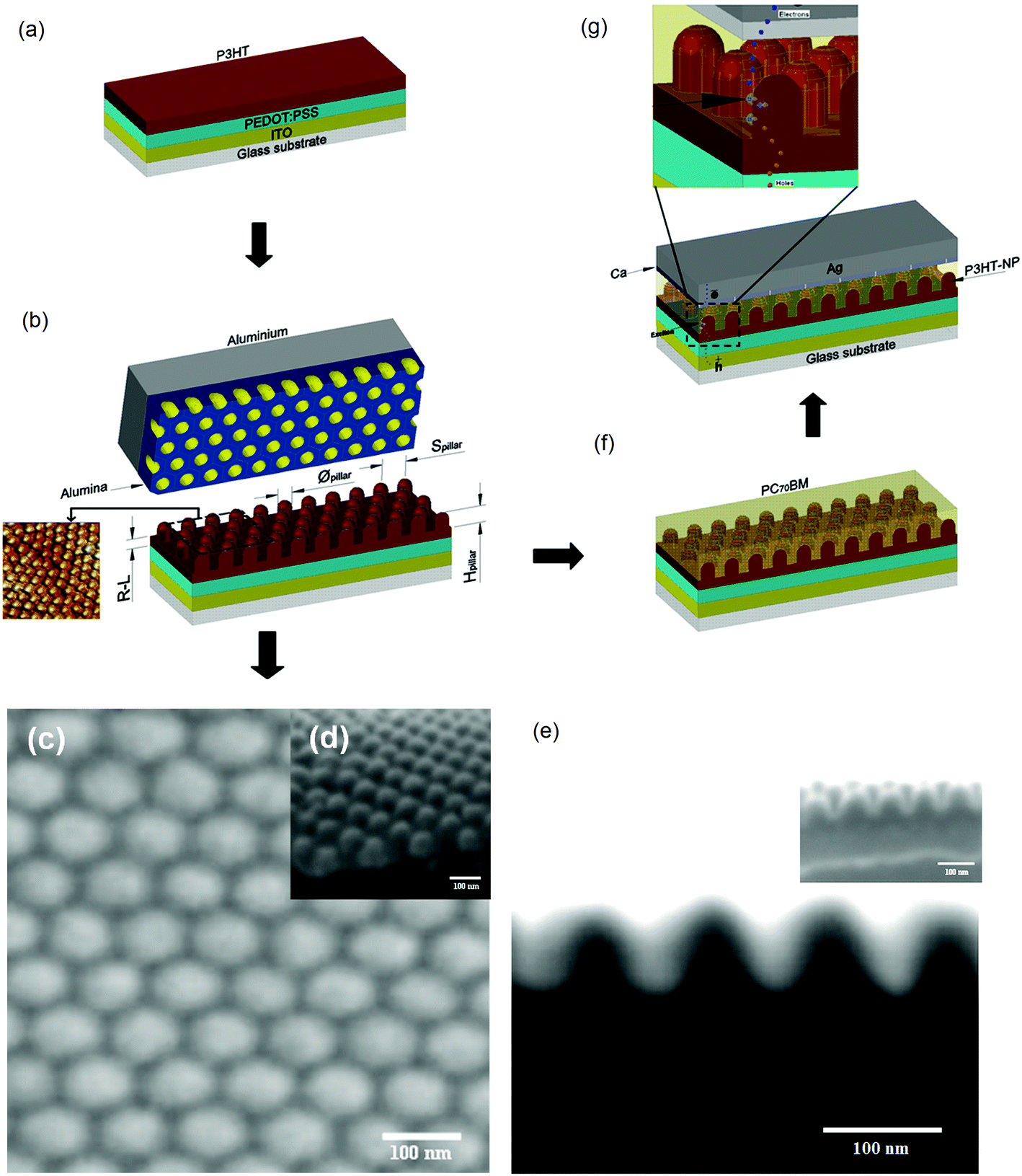 | ||
| Fig. 1 Different steps to obtain the an interdigitated OSC. (a) Spin coating of the P3HT layer on PEDOT:PSS/ITO/glass. (b) Patterning of the P3HT-NP structure done by soft nanoimprinting combining with NAAT templates. The geometrical characteristics of the P3HT-NP can be seen. ϕpillar is the diameter of the nanopillar, Hpillar is the height of the nanopillar, Spillar is the distance between the nanopillars and RL is the residual layer of the structure. (c) Top-view of the P3HT-NP with excellent replication by the applied soft NAAT with ϕpillar = 60 ± 4 nm. (d) Tilt view and (e) cross section of the P3HT-NP with Hpillar = 80 ± 3 nm, Spillar = 100 ± 5 nm and RL = 45 ± 3 nm. (f) Deposition by spin coating of PC70BM using an anisole solvent on the P3HT-NP. (g) Deposition of calcium and silver by thermal evaporation on the previous layers to obtain the IHJN-OSC. | ||
The thickness of the P3HT layer was measured by profilometry to be 130 nm. Then, a soft nanoimprinting process was applied to the prepared NAATs with an antiadhesion layer to imprint the polymer. A hydraulic charge pressure was applied in combination with the temperature to produce nanopillars on the P3HT layer. Finally, the template was released from the sample, and the polymer nanoimprinting with a negative replication of the template was obtained (see Fig. 1(b)). We optimized the soft nanoimprinting conditions (i.e. time, pressure and temperature) to ensure the fidelity of the nanoporous patterns from the NAAT for the P3HT nanopillars, as described in the Experimental section. The geometric parameters that define the P3HT-NP are the pillar diameter (ϕpillar), pillar height (Hpillar), interpillar distance (Spillar) and residual layer (RL). Fig. 1(c), (d) and (e) show top-view, tilt-view and cross section-view ESEM images of the P3HT-NP, respectively. The P3HT-NPs have an average ϕpillar = 60 ± 4 nm, Hpillar = 80 ± 3 nm, Spillar = 100 ± 5 nm and RL = 40 ± 3 nm with an aspect ratio of 1.3. Subsequently, the PC70BM fullerene material was deposited by spin coating directly on top of the P3HT-NP layer using an anisole solution (2 wt%), as is shown in Fig. 1(f). In this study, we chose PC70BM for two reasons. First, the material has a relatively strong and broad absorption in the visible range from 400 nm to 700 nm and gives better results for photon harvesting in the active layer than when other fullerenes such as C60, C70 and PCBM are used.41 The literature only reports interdigitated nanostructured OSCs fabricated with C60 and PCBM, not with PC70BM. Second, PC70BM can be dissolved in anisole solvent and deposited by spin coating onto the P3HT-NP. The spaces between the P3HT nanopillars were filled with the PC70BM mixture and the anisole solvent. The nanoimprinting polymer layer was not destroyed when the mixture was deposited.42,43 Dichloromethane (CH2Cl2) has sometimes been used to dissolve the PCBM and fabricate the nanostructured OSC.10,16,17 Anisole is another solvent that may potentially be used for the fabrication of nanostructured cells. There are some reports about anisole solvent being used to fabricate organic thin film transistors (OTFT), where the various polymer layers have to be deposited using orthogonal solvents.42,44 In this study, it is worth noting that PC70BM is used in combination with the anisole solvent. It is the first time that this method has been used to deposit PC70BM into the gaps of the P3HT-NPs to get the IHJN-OSC. Subsequently, the samples were placed inside the evaporation chamber, where a thin layer of calcium (Ca) and silver (Ag) were evaporated as a top contact (parameters and conditions are given in the Experimental section), as is shown in Fig. 1(g).
Fig. 2(a) shows the cross section-view of an IHJN-OSC structure captured by ESEM. On some samples infiltrated with the fullerene material (P3HT-NP/PC70BM), Ca (20 nm) and one thin layer of Ag (10 nm) were deposited so that the stacked material covered the top surface of the previous active layer (see Fig. 2(b)). Finally, Fig. 2(c) shows the top view of the top surface of the Ag metal contact with a thickness of 100 nm.
 | ||
| Fig. 2 (a) ESEM images from the cross section of an IHJN-OSC with the stack ITO/PEDOT:PSS/P3HT-NP/PC70BM/Ca/Ag. (b) Top view after the evaporation of Ca (20 nm) and Ag (10 nm) onto the surface of PC70BM/P3HT-NP, (c) Top view of the Ca/Ag metal contact with thicknesses of 20 nm/100 nm, respectively. | ||
Two types of control cells based on BHJ-OSC standard blend films (by spin coating from a mixture solution) and BL-OSCs (by non-patterned imprinting) were fabricated for the purpose of comparison (parameters and conditions are given in the Experimental section). The BHJ-OSCs have the architecture ITO/PEDOT:PSS/P3HT:PC70BM/Ca/Ag and the BL-OSCs have the stack ITO/PEDOT:PSS/P3HT/PC70BM/Ca/Ag.
Atomic force microscopy (AFM) in tapping mode was applied to the P3HT-NP, P3HT:PC70BM-BHJ and P3HT-single layers after thermal annealing in order to get further insight into their respective surface areas (see Fig. S3 in ESI†).
Fig. 3(a) shows the UV-vis spectroscopy for the pristine P3HT-NP, P3HT flat film and P3HT/PC70BM-IHJN, P3HT:PC70BM-BHJ and P3HT/PC70BM-BL films which were studied. In the UV-vis spectra, we see that the absorbance of the P3HT nanopillar films is 13% higher than that of the P3HT flat film at 510 nm, which is consistent with previous reports.11,13 A small red-shift was observed for the imprinted film compared to the flat film. Moreover, the imprinted P3HT-NPs showed a pronounced increase in the shoulder centered at ∼605 nm, the intensity of which is correlated with the degree of P3HT crystallinity. This is attributed to the fact that P3HT has a greater conjugation length and a more ordered structure than the P3HT flat film because of the self-organization of the mobile chains that is done during the heating and imprinting of the film compared to the P3HT flat film.24 Thermal annealing was applied during and after imprinting and mainly helped to remove residual solvent and reduce the free volume, which led to a closer packing of the polymer chains and improved mobility of the holes.45 To enhance the absorbance when the nanopillars were used, the geometry had to be optimum (i.e. pillar diameter, pillar height and interpillar distance) so that the light trapping ability inside the structure was also optimum, as some simulations have shown.46 The UV-vis spectra are also shown for the P3HT/PC70BM-IHJN, P3HT:PC70BM-BHJ and P3HT/PC70BM-BL films with the deposited fullerene material and the absorptions are observed to be stronger at 490 nm and 380 nm, corresponding to the P3HT and PC70BM materials, respectively. P3HT:PC70BM-BHJ showed the highest absorption while P3HT/PC70BM-BL presented the lowest. This was due to the fact that the active layer of BHJ presented a film thickness of 200 ± 10 nm, while the active layers of the IHJN and BL films were 160 ± 5 nm and 170 ± 5 nm, respectively. The absorbance peak intensity of the P3HT/PC70BM-IHJN film was 9% greater than that of the P3HT/PC70BM-BL film. Moreover, the P3HT/PC70BM-IHJN showed a considerably higher absorbance (at 600 nm) than that of the P3HT:PC70BM-BHJ film. The PL measurements for all the structures are shown in Fig. S4 and explained in the ESI.†
 | ||
| Fig. 3 (a) UV-Visible absorbance of the P3HT-nanopillars (red open circles) and the P3HT-film (green open squares). The absorbance spectra of the IHJN-[P3HT/PC70BM] (red dashed line), BHJ-[P3HT:PC70BM] (green continuous line) and BL-[P3HT/PC70BM] (blue dotted line) films are also shown. (b) The IPCE spectra of the IHJN-OSC, BHJ-OSC and BL-OSC. | ||
Fig. 3(b) compares the incident photon to the current efficiency (IPCE) spectra for the OSC devices with P3HT/PC70BM-IHJN, P3HT:PC70BM-BHJ and P3HT/PC70BM-BL. It can be observed that the trends of the IPCE spectra are similar to those of the absorption spectra throughout the range, but particularly between 400 nm and 700 nm. The IPCE of the P3HT/PC70BM-IHJN, P3HT:PC70BM-BHJ and P3HT/PC70BM-BL organic solar cells at 550 nm were 50%, 57% and 45%, respectively. By integrating the IPCE curves we determined the short circuit current density for the P3HT/PC70BM-IHJN, P3HT:PC70BM-BHJ and P3HT/PC70BM-BL and they were 6.99 mA cm−2, 7.67 mA cm−2 and 6.7 mA cm−2, respectively, which are strongly supported by the J–V characteristics, as will be seen below.
Fig. 4(a) illustrates the current–voltage (J–V) characteristics of the P3HT/PC70BM-IHJN imprinted solar cells in comparison to the P3HT:PC70BM-BHJ and P3HT/PC70BM-BL OSC controls under solar illumination at 1 sun (100 mW cm−2). Table 1 summarizes the best and average performance parameters (i.e. open circuit voltage (VOC), short circuit current density (JSC), fill factor (FF) and power conversion efficiency (PCE) of the IHJN-OSCs (twenty devices), BHJ-OSCs (fifteen devices) and BL-OSCs (fifteen devices) after fabrication. The best results of the three structures were analyzed.
 | ||
| Fig. 4 (a) J–V curves of the IHJN-OSC (red dashed line), BHJ-OSC (green continuous line) and BL-OSC (blue dotted line) under light (1 sun = 100 mW cm−2). (b) Semi-log J–V curves under darkness for the three structures. | ||
| P3HT/PC70BM |
V
OCa (mV) |
J
SCb (mA cm−2) |
FFc (%) | PCEd (%) |
R
S0-ile (Ω cm2) |
R
SH0-ilf (kΩ cm2) |
R
S0-dkg (Ω cm2) |
R
SH0-dkh (kΩ cm2) |
|
|---|---|---|---|---|---|---|---|---|---|
| a Open circuit voltage. b Short circuit current. c Fill factor. d Power conversion efficiency. The illumination intensity equivalent applied was 100 mW cm−2 after spectral mismatch correction using an AM 1.5G solar simulator. e Series resistance per unit area under illumination. f Shunt resistance per unit area under illumination. g Series resistance per unit area under dark. h Shunt resistance per unit area under dark. | |||||||||
| A | IHJN-OSC | 613 ± 10 | 6.4 ± 0.5 | 53.2 ± 5.6 | 2.3 ± 0.2 | 2.58 ± 0.41 | 0.19 ± 0.06 | 3.06 ± 0.44 | 1821.07 ± 1093.95 |
| B | IHJN-OSC best | 630 | 7.1 | 61.3 | 2.6 | 2.00 | 0.26 | 2.18 | 603.09 |
| C | BHJ-OSC | 594 ± 2 | 6.8 ± 0.4 | 50.1 ± 1.2 | 2.0 ± 0.2 | 7.71 ± 1.01 | 0.31 ± 0.02 | 11.37 ± 2.54 | 2067.50 ± 634.63 |
| D | BHJ-OSC best | 598 | 7.7 | 51.4 | 2.4 | 6.62 | 0.33 | 8.72 | 2580.01 |
| E | BL-OSC | 569 ± 41 | 6.5 ± 0.4 | 43.2 ± 5.1 | 1.6 ± 0.4 | 2.93 ± 0.44 | 0.17 ± 0.04 | 3.22 ± 0.35 | 2.11 ± 1.47 |
| F | BL-OSC best | 612 | 6.8 | 49.0 | 2.1 | 2.43 | 0.21 | 2.56 | 3.60 |
The IHJN-OSC, BHJ-OSC and BL-OSC showed a PCE of 2.6%, 2.4% and 2.1%, respectively. The VOC, FF and PCE of the IHJN-OSC were 3.5%, 19.3% and 8.3% higher than the BHJ-OSC, respectively. On the other hand, the JSC of the IHJN-OSC was 7.8% less than that of BHJ-OSC. The PCE of the BHJ-OSC was a little less than that of IHJN-OSC because the active layer was thicker, so that it could be compared with the others. Moreover, the VOC, JSC, FF and PCE of the IHJN-OSC were 1%, 5%, 23% and 24% higher than the BL-OSC, respectively.
In this study, we have observed that the enhancement in the PCE of the IHJN-OSCs principally originated from the improvements in FF. The FF for the BHJ-OSCs and BL-OSCs were low values. The increase in the performance yield of the JSC of the IHJN-OSCs can be argued by two aspects. First, it can be attributed to the well-controlled interdigitated heterojunction morphology of both materials (P3HT-NP and PC70BM) which increased their interfacial area and the contact between them, and made the exciton dissociation more efficient (to get free electrons and holes). Then, the electrons and holes travel through their respective materials to be collected in the metal contact.14,16 Second, another reason for the increase in JSC is that the π–π stacking in the P3HT polymer is better oriented and the crystals are better formed throughout the nanopillar. This is due to the induction that the polymer undergoes when it is introduced into the nanopore of the template during the soft imprinting step. Therefore, the charge carriers (holes) will move through the P3HT structure and the nanopillar with less difficulty.24 The improvement in the crystallinity favors the charge-mobility of holes and the charge transport along the P3HT-NP pathways and reduces the recombination of charge carriers on the pathways. This hypothesis was confirmed by analyzing the orientations of the nanopillar morphology of the molecular P3HT with micro-X-ray diffraction.27 The P3HT side chains were found to be parallel with the axial direction of the nanopillars, similar results were also reported by other publications.19,24,29 It should be pointed out that although the absolute thickness of the IHJN-OSC was 10 nm less than that BL-OSC, the JSC was slightly greater. Moreover, the JSC in the P3HT:PC70BM-BHJ solar cell was highest because the active layer was thicker and so it was able to absorb more photons.11
The increase of the superficial area of the P3HT-NP layer with respect to the P3HT flat film is known as the interface enhancement factor (IEF), which was calculated by applying eqn (1):10,13,24
 | (1) |
The FF was highest for the IHJN-OSC (∼61.3%) in comparison with the BHJ-OSC (∼51.4%) and BL-OSC (∼49.0%). This increase in FF for the IHJN-OSC can be attributed to the nanoimprinted pattern – in which the interface area between the polymer/fullerene material was greater –, the good quality of the cathode-fullerene and anode-polymer interfaces and the decrease in the series resistance (RS) in the interdigitated heterojunction nanomorphology, all of which suggest that the charge transport properties are substantially improved, as has been observed by other researchers.9,37,47
Fig. 4(b) shows the J–V characteristics in dark conditions for the three organic solar cells. It is well known that RS can be related to the resistance and thickness of the active layer, the contact resistance between the metal and active layers, the transport properties of the semiconductor material and the properties of the selective contacts. Its value per unit area, RS0, can be calculated by the inverse slope of the J–V curve at the highest operating voltage where the curve becomes linear: RS0 = (J /V)−1, as has been reported in ref. 48,49. In this study, the series resistances RS0-il and RS0-dk were obtained from the J–V characteristics under illumination and darkness, respectively, and the values for each organic solar cell structure are shown in Table 1. In general, RS0-il and RS0-dk on the IHJN-OSC presented the best values, which where 70% and 75% lower than BHJ-OSC and 18% and 15% lower than BL-OSC, respectively.
The shunt resistance, RSH, which is related to the recombination of charge carriers near the dissociation site (e.g. the donor/acceptor interface of the interdigitated organic materials, P3HT-NP/PC70BM in this case), also depends on the transport properties of the semiconductor. The value of the shunt resistance per unit area, RSH0, can be determined by calculating the inverse slope at around 0 V of the J–V curve, RSH0 = (J/V)−1. In the dark, this parallel shunt resistance is expected to reflect the intrinsic conductivity of the materials. Under illumination, light-induced charge generation (photodoping), caused by the charge transfer between the donor and the acceptor, is expected to reduce the shunt dramatically, as was observed in our previous results.50 In this study, the shunt resistances RSH0-il and RSH0-dk were obtained from the J–V characteristics under illumination and darkness, respectively, and their values are shown in Table 1. Continuing with the analysis, in general the RSH0-il and RSH0-dk of the IHJN-OSC were 21% and 76% lower than those of the BHJ-OSC, but were 1.23 times and 167 times higher than those of the BL-OSC, respectively.
The VOC of the IHJN-OSC was 3.5% and 1.1% greater than that of the BHJ-OSC and BL-OSC, respectively. The improvement in VOC with respect to the blend devices might be attributed to a reduction in shunt losses, as the wetting layers were correctly arranged in the imprinted devices, as reported previously.11 It is also reported in the literature that VOC can be attributed to differences in the electrical contact work functions and to the difference between the HOMO of the donor and the LUMO of the acceptor.4,21 However, when there are recombination losses, the real VOC value depends on the inverse saturation current of the junction in the dark.50 The VOC value for the IHJN and BL organic solar cells are almost identical. On the other hand, the VOC value for the BHJ-OSC is 6% less than for the IHJN and BL organic solar cells at 1 sun. This must be because, in the IHJN and BL cells, the PEDOT:PSS selective electrode is only in contact with the donor material while the calcium selective electrode is in contact with the acceptor material. The donor and acceptor materials of the BHJ cells, however, are in close contact at the same time with both selective contacts.
Table 2 summarizes the methods for fabricating the nanostructured organic solar cells and compares their geometric characteristics that have been reported in literature with our results.
| Polymer- fullerene | Morphology array | Type of template useda | Solventb | Method of manufacture of donor–acceptorc | Feature size W or ϕ, H, Sd (nm) | A/A0e (nm2) | RLf (nm) | Ref. | |
|---|---|---|---|---|---|---|---|---|---|
| a NAAT is nanoporous anodic alumina template. b Solvents used to dissolve the fullerene material: CH2Cl2 is dichloromethane, CHCl3 is chloroform, and C7H8O is anisole. c MW is melt wetting, EV is evaporation, NI is nanoimprinting, SC is spin coating, SANIL is solvent assisted nanoimprint lithography, and EBL is electron-beam lithography. d W is the width for nanograting morphology or ϕ is the diameter for the dot, rod and nanopillar morphologies, H is the height and S is the pitch or distance between the nanostructures. e A/A0 is the ratio of D/A interface areas of the patterned to the planar-interface photovoltaic devices and this was calculated using eqn (1). f Residual layer that is under the nanostructure. g Results from this contribution. | |||||||||
| A | P3HT/C60 | Rod | NAAT | — | MW/EV | 50, 150, 100 | 3.3 | 30 | 13 |
| B | P3HT/PCBM | Rod | NAAT | CH2Cl2 | NI/SC | 50, 80, 100 | 2.2 | 20 | 10 |
| C | P3HT/PCBM | Dot | Silicon | CHCl3 | SANIL/SC-SANIL | 25, 80, 50 | 3.5 | 10 | 11 |
| D | P3HT/PCBM | Rod | Silicon | CH2Cl2 | NI/SC | 80, 60, 100 | 2.5 | — | 14 |
| E | P3HT/PCBM | Nanograting | Silicon | CH2Cl2 | SANIL/SC | 137, 56, 360 | 1.2 | — | 15 |
| F | P3HT/PCBM | Nanopillar | NAAT | CH2Cl2 | NI/SC | 30, 180, 90 | 3.0 | — | 16 |
| G | P3HT/PCBM | Nanopillar | — | CH2Cl2 | EBL/SC | 50, 60, 200 | 1.2 | 25 | 17 |
| P3HT/PC70BM | Nanopillar | NAAT | C7H8O | NI/SC | 60, 80, 100 | 2.5 | 40 | — | |
Likewise, Table 3 summarizes the performance parameters of the structures shown in Table 2. It is worth noting that our IHJN-OSC is one of the first to be manufactured by spin coating using PC70BM and an anisole solvent and deposited on P3HT-NP. The fill factor obtained here of 61.3% is higher than all others reported in the literature. The PCE of the IHJN-OSC was 2.6%, which is comparable with other standard methods and technologies such as a standard NIL mold, NAAT and double imprinting.
| Device structure |
V
OCa (mV) |
J
SCb (mA cm−2) |
FFc (%) | PCEd (%) | Ref. | |
|---|---|---|---|---|---|---|
| a Open circuit voltage. b Short circuit current. c Fill factor. d Power conversion efficiency. The illumination intensity equivalent applied was at 100 mW cm−2 after the spectral mismatch correction using an AM 1.5G solar simulator. e Results from this contribution. | ||||||
| A | ITO/PEDOT:PSS/P3HT nanorods/C60 (200 nm)/LiF (0.6 nm)/Al (150 nm) | 510 | 4.7 | 46.0 | 1.12 | 13 |
| B | ITO/PEDOT:PSS/P3HT nanorods/PCBM(70 nm)/LiF (0.7 nm)/Al (80 nm) | 570 | 0.1 | 56.0 | 0.05 | 10 |
| C | ITO/PEDOT:PSS/P3HT nanodots/PCBM (80 nm)/Al (80 nm) | 640 | 8.6 | 56.0 | 3.25 | 11 |
| D | ITO/PEDOT:PSS/P3HT nanorods/PCBM (70 nm)/Al (100 nm) | 570 | 11.3 | 40.0 | 2.57 | 14 |
| E | ITO/PEDOT:PSS/P3HT nanograting/PCBM (69 nm)/Al (100 nm) | 582 | 7.6 | 58.0 | 2.59 | 15 |
| F | ITO/PEDOT:PSS/P3HT nanopillars/PCBM (? nm)/Al (100 nm) | 600 | 7.4 | 53.0 | 2.40 | 16 |
| G | ITO/PEDOT:PSS/P3HT nanopillars/PCBM (40 nm)/Al (100 nm) | 600 | 1.7 | 40.0 | 0.43 | 17 |
| ITO/PEDOT:PSS/P3HT nanopillars/PC70BM (40 nm)/Ca (20 nm)/Ag (100 nm) | 619 | 7.1 | 61.3 | 2.60 | — | |
Fig. 5(a) shows typical CE transients for the devices at 1 sun and in VOC conditions, and an extraction half-time of ∼8 μs for the BHJ-OSC as reported in the literature.51 For the IHJN-OSC and BL-OSC, on the other hand, the half-time was ∼6 μs.
 | ||
| Fig. 5 (a) CE transient acquired to compare the IHJN-OSC, BHJ-OSC and BL-OSC under 1 sun steady state background irradiation. For the CE transient, the background irradiation was turned off rapidly, and the device was simultaneously switched from an open to a short circuit. (b) Charge carrier density (n) as a function of the applied bias (the maximum point of each curve is 1 sun of light incident on the PV structure during the measurement). In the IHJN-OSC, BHJ-OSC and BL-OSC the charge carrier density undergoes an exponential increase. (c) Logn-light intensity, variation in charge carrier density measured under different light intensities for each structure manufactured. | ||
The CE was used to measure the average charge carrier density (n) in the device at various white light intensities while holding the device at VOC after switching off the light. The light intensities go from dark to 1 sun.
These measurements of n against voltage are shown in Fig. 5(b). Note that this experiment collects charges stored in both the photoactive layer and the electrodes. The extracted charge n at 1 sun for the IHJN-OSC, BHJ-OSC and BL-OSC with VOC was ∼630 mV, 598 mV and 612 mV, where n values were 5.5 × 1016 cm−3, 1.3 × 1017 cm−3 and 3.8 × 1016 cm−3, respectively. These values have a strong correlation with the JSC of the J–V characteristic obtained for each structure analyzed. As has been explained before,51 the charge carrier density in the BHJ-OSC manufactured with P3HT:PC70BM can be produced in the bulk of the active layer and at the selective electrodes of the device. Generally, the volumetric charge density in the P3HT:fullerene active layer is more predominant than at the selective electrodes. Our devices with structures of BHJ-OSC, IHJN-OSC and BL-OSC seem to have the same predominant charge accumulation dynamics.38,39,48,51Fig. 5(b) and (c) show that the charge carrier density in open circuit conditions for different light intensities exponentially depends on the VOC obtained by changing the light intensity according to the following formula (eqn (2)):47
| n0 = eγVOC | (2) |
TPV measurements were performed on the IHJN-OSC, BHJ-OSC, and BL-OSC. The charge carrier densities obtained from the CE measurements at different light intensities (from 0.3 to 1.0 sun) were used to get the carrier lifetime from the TPV measurements. The decay dynamics for all the devices agree with previous measurements on P3HT:PCBM blends: namely, that single-exponential fits apply for a wide range of illumination intensities.37–39,47,48,53,54Fig. 6(a) shows the carrier lifetimes as a function of carrier density for various illumination intensities. At one sun, the IHJN-OSC, BHJ-OSC and BL-OSC have carrier lifetimes of ∼3.9 μs, ∼5.8 μs and 4.2 μs, respectively. The recombination lifetime decreases when the light intensity increases, until 1 sun is achieved, and the number of charge carriers also increases.
 | ||
| Fig. 6 (a) TPV measurements were performed under open circuit conditions and different illuminations (VOC) for the IHJN-OSC, BHJ-OSC and BL-OSC structures. (b) Bimolecular recombination rate constants krec, extracted from the carrier τ and n, as a function of n. The pulse excitation wavelength was 470 nm. The pulsed source power was set so that the ΔV of the TPV measurement did not exceed 3% of the VOC measured at 0.1 sun. | ||
The charge density has an inverse square relationship with the recombination lifetime (eqn (3)) with β/γ = λ. The IHJN-OSC, BHJ-OSC and BL-OSC show λ values of 2.4, 2 and 1.8, respectively.
| τΔn = τn0(n0/n)λ | (3) |
All values of λ indicate that there are bimolecular recombinations, with similar values reported in the literature.37,39,48Fig. 6(b) shows the bimolecular recombination rate constants krec and were calculated from the carrier lifetimes and densities according to the following eqn (4):51
| krec = 1/(λ + 1)τΔn | (4) |
The devices with the lowest bimolecular recombination rate were the BHJ-OSCs. Reduced recombination constants are considered critical for efficient solar cells. The BHJ-OSCs had the longest carrier lifetimes and the smallest krec values, whereas the BL-OSCs had the shortest carrier lifetimes and the largest krec. The IHJN-OSCs presented values in between (see Fig. 6(b)).
All the electrical characterization used in this study provides insight into the working mechanisms of the various organic solar cells that were fabricated and analyzed. The critical parameter(s) required to improve the synthesis, design and fabrication of interdigitated organic solar cells and enhance the performance parameters have been identified.
4. Conclusions
In summary, the IHJN-OSCs were manufactured by soft nanoimprinting in combination with nanoporous anodic alumina templates to produce P3HT-NPs, which were filled by spin coating of PC70BM onto the top of the NPs in combination with an anisole orthogonal solvent. The fabrication method, using this orthogonal solvent, for IHJN-OSCs has been reported for the first time. The P3HT-NPs had good replication and a well-ordered array with NAAT, possessing an average diameter of 60 nm, pillar height of 80 nm and interpillar distance of 100 nm. The IHJN-OSCs were compared with BHJ-OSCs and BL-OSCs as controls, which were fabricated under the same conditions. The surface area of the P3HT-NPs increased to 2.5 times more than that of the BL-OSCs. Current–voltage characteristics and optical measurements were carried out for all photovoltaic devices. The results provide direct evidence that the imprinting layer gives FF ∼ 61.3% and PCE ∼ 2.6%. This is due to the larger interface between the donor and acceptor materials, resulting in more efficient photogeneration, exciton dissociation and charge transport on the extended interfaces made up of a finely controlled morphology. CE and TPV measurements were applied to the IHJN-OSCs. Bimolecular recombination was found to be the main mechanism by which charge carriers were lost. For the interdigitated devices, the recombination losses were lower than for the BL-OSCs. The gamma values for the IHJN-OSCs presented an exponential tail in the density of trap states that extended into the band-gap of the photoactive layer. These values were lower for the IHJN-OSCs than for the BHJ-OSCs and BL-OSCs. In other words, the structure with the lowest energetic disorder in the active layer was the IHJN-OSC, where the recombination process was reduced. The study of the three structures at the same time provides important information about how physical properties such as the charge density, charge carrier lifetime and mechanism are governed inside the device.We conclude that the interdigitated morphology has a favorable influence on photogeneration and charge transport but that they also depend on factors such as the quality of the materials, the fabrication process (e.g. the use of orthogonal solvents, quality of materials, etc.), technology and even how the solar cells are characterized. The use of orthogonal solvents to fabricate solar cells offers a simple and potentially low-cost fabrication route and opens up new possibilities for using new polymers for manufacturing interdigitated OSCs.
Acknowledgements
This work was supported by the Spanish Ministry of Economy and Competitiveness (MINECO) under grant number TEC2012-34397, the ICREA under the ICREA Academia Award and by the Catalan authority under project AGAUR 2014 SGR 1344. EP would like to thank MINECO for the project CTQ2013-47183-R and the support through the Severo Ochoa Excellence Accreditation 2014-2018 (SEV-2013-0319).Notes and references
- C. J. Brabec, Sol. Energy Mater. Sol. Cells, 2004, 83, 273–292 CrossRef CAS PubMed.
- V. S. Balderrama, M. Estrada, A. Viterisi, P. Formentin, J. Pallarés, J. Ferré-Borrull, E. Palomares and L. F. Marsal, Microelectron. Reliab., 2013, 53, 560–564 CrossRef CAS PubMed.
- P. Reiss, E. Couderc, J. De Girolamo and A. Pron, Nanoscale, 2011, 3, 446–489 RSC.
- J.-T. Chen and C.-S. Hsu, Polym. Chem., 2011, 2, 2707–2722 RSC.
- J. Jo, S.I. Na, S.S. Kim, T.W. Lee, Y. Chung, S.J. Kang, D. Vak and D.-Y. Kim, Adv. Funct. Mater., 2009, 19, 2398–2406 CrossRef CAS PubMed.
- W. Ma, C. Yang, X. Gong, K. Lee and A. J. Heeger, Adv. Funct. Mater., 2005, 15, 1617–1622 CrossRef CAS PubMed.
- K. Sivula, Z. T. Ball, N. Watanabe and J. M. J. Fréchet, Adv. Mater., 2006, 18, 206–210 CrossRef CAS PubMed.
- J. Weickert, R. B. Dunbar, H. C. Hesse, W. Wiedemann and L. Schmidt-Mende, Adv. Mater., 2011, 23, 1810–1828 CrossRef CAS PubMed.
- X. Li, W. C. H. Choy, L. Huo, F. Xie, W. E. I. Sha, B. Ding, X. Guo, Y. Li, J. Hou, J. You and Y. Yang, Adv. Funct. Mater., 2012, 24, 3046–3052 CrossRef CAS PubMed.
- W. Wiedemann, L. Sims, A. Abdellah, A. Exner, R. Meier, K. P. Musselman, J. L. MacManus-Driscoll, P. Müller-Buschabaum, G. Scarpa, P. Lugli and L. Schmidt-Mende, Appl. Phys. Lett., 2010, 96, 263109 CrossRef PubMed.
- X. He, F. Gao, G. Tu, D. G. Hasko, S. Hüttner, N. C. Greenham, U. Steiner, R. H. Friend and W. T. S. Huck, Adv. Funct. Mater., 2011, 21, 139–146 CrossRef CAS PubMed.
- M. Yu, Y. Z. Long, B. Sun and Z. Fan, Nanoscale, 2012, 4, 2783–2796 RSC.
- J. S. Kim, Y. Park, D. Y. Lee, J. H. Lee, J. H. Park, J. K. Kim and K. Cho, Adv. Funct. Mater., 2010, 20, 540–545 CrossRef CAS PubMed.
- M. Aryal and F. Buyukserin, J. Vac. Sci. Technol., B, 2008, 26, 2562–2566 CAS.
- J. Y. Park, N. R. Hendricks and K. R. Carter, Langmuir, 2011, 27, 11251–11258 CrossRef CAS PubMed.
- D. Chen, W. Zhao and T. P. Russell, ACS Nano, 2012, 6, 1479–1485 CrossRef CAS PubMed.
- S. Moungthai, N. Mahadevapuram, P. Ruchhoeft and G. E. Stein, ACS Appl. Mater. Interfaces, 2012, 4, 4015–4023 CAS.
- C. W. Tang and S. A. Vanslyke, Appl. Phys. Lett., 1987, 51, 913–915 CrossRef CAS PubMed.
- J. Slota, X. Hea and W. T. S. Huck, Nano Today, 2010, 5, 231–241 CrossRef CAS PubMed.
- K. M. Coakley, Y. Liu, C. Goh and M. D. McGehee, MRS Bull., 2005, 30, 37–40 CrossRef CAS.
- C. J. Brabec, N. S. Sariciftci and J. C. Hummelen, Adv. Funct. Mater., 2001, 11, 15–26 CrossRef CAS.
- H. Hoppe and N. S. Sariciftci, J. Mater. Chem., 2006, 16, 45–61 RSC.
- V. S. Balderrama, M. Estrada, A. Cerdeira, B. S. Soto-Cruz, L. F. Marsal, J. Pallares, J. C. Nolasco, B. Iñiguez, E. Palomares and J. Albero, Microelectron. Reliab., 2011, 51, 597–601 CrossRef CAS PubMed.
- Y. Yang, K. Mielczarek, M. Aryal, A. Zakhidov and W. Hu, ACS Nano, 2012, 6, 2877–2892 CrossRef CAS PubMed.
- L. Zhao, S. Zhao, Z. Xu, Q. Yang, D. Huang and X. Xu, Nanoscale, 2015, 7, 5537–5544 RSC.
- Y. Liu, C. Kirsch, A. Gadisa, M. Aryal, S. Mitran, E. T. Samulski and R. Lopez, J. Phys. D: Appl. Phys., 2013, 46, 024008 CrossRef.
- A. Santos, P. Formentín, J. Pallarés, J. Ferré-Borrull and L. F. Marsal, Sol. Energy Mater. Sol. Cells, 2010, 94, 1247–1253 CrossRef CAS PubMed.
- J. H. Lee, D. W. Kim, H. Jang, J. K. Choi, J. Geng, J. W. Jung, S. C. Yoon and H.-T. Jung, Small, 2009, 5, 2139–2143 CrossRef CAS PubMed.
- M. Aryal, K. Trivedi and W. Hu, ACS Nano, 2009, 3, 3085–3090 CrossRef CAS PubMed.
- A. Greiner and J. H. Wendorff, Angew. Chem., Int. Ed., 2007, 46, 5670–5703 CrossRef CAS PubMed.
- F. C. Krebs, Sol. Energy Mater. Sol. Cells, 2009, 93, 394–412 CrossRef CAS PubMed.
- N. Haberkorn, J. S. Gutmann and P. Theato, ACS Nano, 2009, 3, 1415–1422 CrossRef CAS PubMed.
- H. Masuda, H. Yamada, M. Satoh and H. Asoh, Appl. Phys. Lett., 1997, 71, 2770–2772 CrossRef CAS PubMed.
- A. Santos, P. Formentin, J. Pallarés, J. Ferré-Borrull and L. F. Marsal, Mater. Lett., 2010, 64, 371–374 CrossRef CAS PubMed.
- A. P. Li, F. Müller, A. Birner, K. Nielsch and U. Gösele, J. Appl. phys., 1998, 84, 6023–6026 CrossRef CAS PubMed.
- D. Cheyns, K. Vasseur, C. Rolin, J. Genoe, J. Poortmans and P. Heremens, Nanotechnol., 2008, 19, 424016–424021 CrossRef CAS PubMed.
- J. Albero, Y. Zhou, M. Eck, F. Rauscher, P. Niyamakom, I. Dumsch, S. Allard, U. Scherf, M. Kruger and E. Palomares, Chem. Sci., 2011, 2, 2396–2401 RSC.
- A. Maurano, R. Hamilton, C. G. Shuttle, A. M. Ballantyne, J. Nelson, B. O'Regan, W. Zhang, I. McCulloch, H. Azimi, M. Morana, C. J. Brabec and J. R. Durrant, Adv. Mater., 2010, 22, 4987–4992 CrossRef CAS PubMed.
- A. Guerrero, N. F. Montcada, J. Ajuria, I. Etxebarria, R. Pacios, G. Garcia-Belmonte and E. Palomares, J. Mater. Chem. A, 2013, 1, 12345–12354 CAS.
- B. C. O'Regan and J. R. Durrant, J. Phys. Chem. B, 2006, 110, 8544–8547 CrossRef PubMed.
- F. Zhang, Z. Zhuo, J. Zhang, X. Wang, X. Xu, Z. Wang, Y. Xin, J. Wang, J. Wang, W. Tang, Z. Xu and Y. Wang, Sol. Energy Mater. Sol. Cells, 2012, 97, 71–77 CrossRef CAS PubMed.
- M. Estrada, I. Mejia, A. Cerdeira and B. Iñiguez, Solid-State Electron., 2008, 52, 53–59 CrossRef CAS PubMed.
- J. S. Jaworski, M. Cembor and M. Orlik, J. Electroanal. Chem., 2005, 582, 165–170 CrossRef CAS PubMed.
- I. Mejia, M. Estrada and M. Avila, Microelectron. Reliab., 2008, 48, 1795–1799 CrossRef CAS PubMed.
- F. Padinger, R. S. Rittberger and N. S. Sariciftci, Adv. Funct. Mater., 2003, 13, 85–88 CrossRef CAS PubMed.
- P. Granero, V. S. Balderrama, J. Ferré-Borrull, J. Pallarès and L. F. Marsal, J. Appl. Phys., 2013, 113, 043107 CrossRef PubMed.
- A. Maurano, C. G. Shuttle, R. Hamilton, A. M. Ballantyne, J. Nelson, W. Zhang, M. Heeney and J. R. Durrant, J. Phys. Chem. C, 2011, 115, 5947–5957 CAS.
- C. G. Shuttle, B. O'Regan, A. M. Ballantyne, J. Nelson, D. D. C. Bradley, J. de Mello and J. R. Durrant, Appl. Phys. Lett., 2008, 92, 093311 CrossRef PubMed.
- V. S. Balderrama, M. Estrada, P. L. Han, P. Granero, J. Pallarés, J. Ferré-Borrull and L. F. Marsal, Sol. Energy Mater. Sol. Cells, 2014, 125, 155–163 CrossRef CAS PubMed.
- C. Waldauf, M. C. Scharber, P. Schilinsky, J. A. Hauch and C. J. Brabec, J. Appl. Phys., 2006, 99, 104503 CrossRef PubMed.
- C. G. Shuttle, A. Maurano, R. Hamilton, B. O'Regan, J. C. de Mello and J. R. Durrant, Appl. Phys. Lett., 2008, 93, 183501 CrossRef PubMed.
- C. G. Shuttle, R. Hamilton, J. Nelson, B. C. O'Regan and J. R. Durrant, Adv. Funct. Mater., 2010, 20, 698–702 CrossRef CAS PubMed.
- C. G. Shuttle, R. Hamilton, B. C. O'Regan, J. Nelson and J. R. Durrant, Proc. Natl. Acad. Sci. U. S. A., 2010, 107, 16448–16452 CrossRef CAS PubMed.
- I. Etxebarria, A. Guerrero, J. Albero, G. Garcia-Belmonte, E. Palomares and R. Pacios, Org. Electron., 2014, 15, 2756–2762 CrossRef CAS PubMed.
- J. W. Krumpfer and T. J. McCarthy, Langmuir, 2011, 27, 11514–11519 CrossRef CAS PubMed.
Footnote |
| † Electronic supplementary information (ESI) available. See DOI: 10.1039/c5nr02429c |
| This journal is © The Royal Society of Chemistry 2015 |