DOI:
10.1039/C5NR01785H
(Paper)
Nanoscale, 2015,
7, 11334-11351
Engineering nanostructured polymer blends with controlled nanoparticle location for excellent microwave absorption: a compartmentalized approach
Received
20th March 2015
, Accepted 21st May 2015
First published on 25th May 2015
Abstract
In order to obtain better materials, control over the precise location of nanoparticles is indispensable. It is shown here that ordered arrangements of nanoparticles, possessing different characteristics (electrical/magnetic dipoles), in the blend structure can result in excellent microwave absorption. This is manifested from a high reflection loss of ca. −67 dB for the best blend structure designed here. To attenuate electromagnetic radiation, the key parameters of high electrical conductivity and large dielectric/magnetic loss are targeted here by including a conductive material [multiwall carbon nanotubes, MWNTs], ferroelectric nanostructured material with associated relaxations in the GHz frequency [barium titanate, BT] and lossy ferromagnetic nanoparticles [nickel ferrite, NF]. In this study, bi-continuous structures were designed using 50/50 (by wt) blends of polycarbonate (PC) and polyvinylidene fluoride (PVDF). The MWNTs were modified using an electron acceptor molecule, a derivative of perylenediimide, which facilitates π–π stacking with the nanotubes and stimulates efficient charge transport in the blends. The nanoscopic materials have specific affinity towards the PVDF phase. Hence, by introducing surface-active groups, an ordered arrangement can be tailored. To accomplish this, both BT and NF were first hydroxylated followed by the introduction of amine-terminal groups on the surface. The latter facilitated nucleophilic substitution reactions with PC and resulted in their precise location. In this study, we have shown for the first time that by a compartmentalized approach, superior EM attenuation can be achieved. For instance, when the nanoparticles were localized exclusively in the PVDF phase or in both the phases, the minimum reflection losses were ca. −18 dB (for the MWNT/BT mixture) and −29 dB (for the MWNT/NF mixture), and the shielding occurred primarily through reflection. Interestingly, by adopting the compartmentalized approach wherein the lossy materials were in the PC phase and the conductive materials (MWNT) were in the PVDF phase, outstanding reflection losses of ca. −57 dB (for the BT and MWNT combination) and −67 dB (for the NF and MWNT combination) were noted and the shielding occurred primarily through absorption. Thus, the approach demonstrates that nanoscopic structuring in the blends can be achieved under macroscopic processing conditions and this strategy can further be explored to design microwave absorbers.
Introduction
Electromagnetic interference (EMI) is generated by a wide spread usage of communication devices and prevalent use of supplementary electronic devices, as an offshoot.1 This emitted EM radiation is a novel type of effluent that interferes with the circuitry of nearby appliances and manifests itself as a perturbation in the operation of electronic devices, which can lead to an indecorous operation or malfunction of precise equipment.2–5 With the aim of circumventing problems attributable to this interference, shielding of emitted EM radiation has become a prime requisite. Therefore, with the intention of limiting EM radiation, some obstructive device must be provided to insulate the internals of devices from nearby environments. In this context significant efforts have been made in the past few decades to develop lightweight, corrosion-resistant and easy-to-fabricate EM shielding materials.6–9
EM attenuation is generally controlled by two main factors. It is dominated primarily by reflection when free electrons or holes can carry the mobile charge in the shield and can interact with the electromagnetic field.10 In this context, metals are of primary interest as shielding materials but they suffer from some inconveniences such as cumbersome processing methods, poor flexibility, large weight and susceptibility to corrosion.11 As an alternative, conducting polymer nanocomposites have gained considerable research attention owing to their high strength to weight ratio, good processability, structural flexibilities, and corrosion resistance.11 Furthermore, compared with metals that are controlled at larger length scales, polymer nanocomposites engage complex absorption mechanisms that can be associated to the hierarchy of scales. This is because (1) charge is transported by plasmon or polaritons (quasi-particles), rather than free electrons, (2) nano-electromagnetism is the framework by which the macroscopic behaviour of the nanocomposites is analysed rather than classical electromagnetism, and (3) the formation of multi channels in the matrix where tunnelling effect is important.12 However, in order to achieve high electrical conductivity, often very high concentrations of conducting filler particles are added, which often deteriorate the overall mechanical properties of the composites.11 In this context, a revolutionary change was brought about by carbon nanotubes (CNTs) owing to their capability to form interconnected network-like structures at very low loadings. This is due to their high aspect ratios and inner tube van der Waals interactions.9 The latter results in the agglomeration of CNTs and reduces the effective aspect ratio, leading to lower bulk electrical conductivity in the composites than that predicted theoretically.1,2 Moreover, in the composites, a thin layer of insulating polymer impedes charge transport. Various strategies have been proposed to address the issues related to the challenge of obtaining a uniform dispersion of CNTs in polymer matrix.13,14 It is evident that the electrical conductivity of CNTs depends on π-conjugation.15 It is envisaged that during chemical functionalization of CNTs, this π-conjugation can be affected. Although chemical functionalization allows the harnessing of different functional moieties on the surface of CNTs, which can be utilized to enhance the interfacial adhesion with the matrix, large scale defects in CNTs are indispensable.16 In order to preserve the structural integrity of the CNTs, non-covalent approaches for modifying CNTs have gained interest.17–19 In this strategy, the π-electron cloud on the CNT surface enables the adsorption of various functional moieties.20 This route results in high electrical conductivity in the composites.21 In this context, it is envisaged that by selectively localizing conductive materials in a given phase of a co-continuous blend the bulk electrical conductivity can be tailored.22 In this approach, the effective (local) concentration of the conductive material increases, which facilitates a more interconnected network. This is especially the case with large aspect ratio particles like CNTs.5,23 Absorption is another factor of EM attenuation where the dielectric constant of the samples must be as close as possible to that of air and the shield should contain electric and/or magnetic dipoles that can interact with electric (E) and magnetic (H) vector components of the oscillating incident EM radiation.10 High dielectric constant materials or magnetic particles can generate such types of electric/magnetic dipoles.24 However, these materials also suffer from problems such as irreproducibility and inferior electrical/mechanical properties primarily due to poor dispersion and agglomeration.25
In light of the above-mentioned facts, we employed a unique strategy for controlling the dispersion of nanostructured materials by suitably modifying the surface chemistry of a co-continuous blend of polycarbonate (PC) and polyvinylidene fluoride (PVDF). Two key properties i.e. high electrical conductivity and large dielectric/magnetic loss, were targeted here to design an efficient microwave absorber. The nanostructured materials usually migrate to their preferred phase during processing. In this study, in addition to tuning the dispersion state of the nanostructured materials by suitable modification, their location in the blends was also tailored by facilitating interfacial interaction/reaction. By selectively filling the phases with nanostructured materials possessing different characteristics (such as electrical/magnetic dipoles), unique properties can be realized.26,27 The bulk electrical conductivity of the blend is increased by several orders of magnitude when the nanostructured materials exceed a critical value, known as percolation threshold.28,29 Thus, when the particle concentration is higher than the percolation threshold, the particles are close enough and the transfer of electrons from one particle to the neighbouring one becomes possible. However, further improvement in conductivity requires an addition of large quantities of the material, making processing difficult. Here, we adopted a unique strategy where we controlled the dispersion of MWNTs in the blend by modifying it with a diimide derivative of perylene (PDI), which is synthesized from perylene-3,4,9,10-tetracarboxylic dianhydride (PTCD) and methylene dianiline (MDA). Perylene, a chemically, thermally and photophysically stable dye has been utilized in various optical devices because of its efficient charge transport.30 The perylene molecule is a planar prototype of large π-conjugated molecules, which can easily bind on to the sidewall of MWNTs via π–π stacking, resulting in an increase in the inner tube spacing. While electrical dipoles were realized using PDI modified MWNTs, the other key properties targeted here like high dielectric/magnetic loss were realized using nanoscopic barium titanate (BT) and nickel ferrite (NF) particles. A number of studies on EM attenuation exist where conducting fillers are either distributed in one of the phases in the blends or throughout the composites, and the observed attenuation mostly occurs by reflection.22 In contrast, there is also ample literature where ferromagnetic and ferroelectric materials are used along with conducting MWNTs where the attenuation is driven mainly by absorption.25 However, the literature lacks approaches where the phases of the blends are filled with nanostructures possessing different inherent characteristics. Hence, we believe that by filling one of the phases with a conductive material (here MWNT) that can attenuate the EM radiation by reflection and the other phase with a lossy material (large dielectric/magnetic loss) that can attenuate the EM radiation by absorption can result in a synergistic enhancement in the overall EM attenuation. Interestingly, when the nanostructured materials were localized in different phases, the shielding via absorption was many folds higher than when they were localized in the same or in both the phases. A high shielding effectiveness of −40 dB (at 18 GHz) and a minimum reflection loss of −67 dB (at 17 GHz) was realized for the unique strategy adopted here and more interestingly at low fractions of MWNTs (3.3 vol%), BT (1.24 vol%) and NF (1.38 vol%).
Experimental section
Materials
Polycarbonate (PC, Lexan-143R with MFI of 11 g/10 min) was procured from Sabic (India). PVDF (Kynar-761, with Mw of 440![[thin space (1/6-em)]](https://www.rsc.org/images/entities/char_2009.gif) 000 g mol−1) was kindly provided by Arkema. Nickel ferrite, (NF, NiFe2O4) nanoparticles (with average diameter of 50 nm), barium titanate (BT, BaTiO3) (with an average particle size of 100 nm), 3,4,9,10-perylenetetracarboxylic dianhydride (PTCD), imidazole, 4,4′-methylenedianiline (MDA), 3-aminopropyltriethoxysilane (APTS), H2O2 (30% in water), N,N′-dicyclohexylcarbodiimide (DCC) and dry toluene were procured from Sigma-Aldrich. N,N-Dimethylformamide, chloroform, and tetrahydrofuran were obtained from commercial sources. Pristine MWNTs (with an average diameter and length of 9.5 nm and 1.5 μm, respectively) were procured from Nanocyl SA (Belgium).
000 g mol−1) was kindly provided by Arkema. Nickel ferrite, (NF, NiFe2O4) nanoparticles (with average diameter of 50 nm), barium titanate (BT, BaTiO3) (with an average particle size of 100 nm), 3,4,9,10-perylenetetracarboxylic dianhydride (PTCD), imidazole, 4,4′-methylenedianiline (MDA), 3-aminopropyltriethoxysilane (APTS), H2O2 (30% in water), N,N′-dicyclohexylcarbodiimide (DCC) and dry toluene were procured from Sigma-Aldrich. N,N-Dimethylformamide, chloroform, and tetrahydrofuran were obtained from commercial sources. Pristine MWNTs (with an average diameter and length of 9.5 nm and 1.5 μm, respectively) were procured from Nanocyl SA (Belgium).
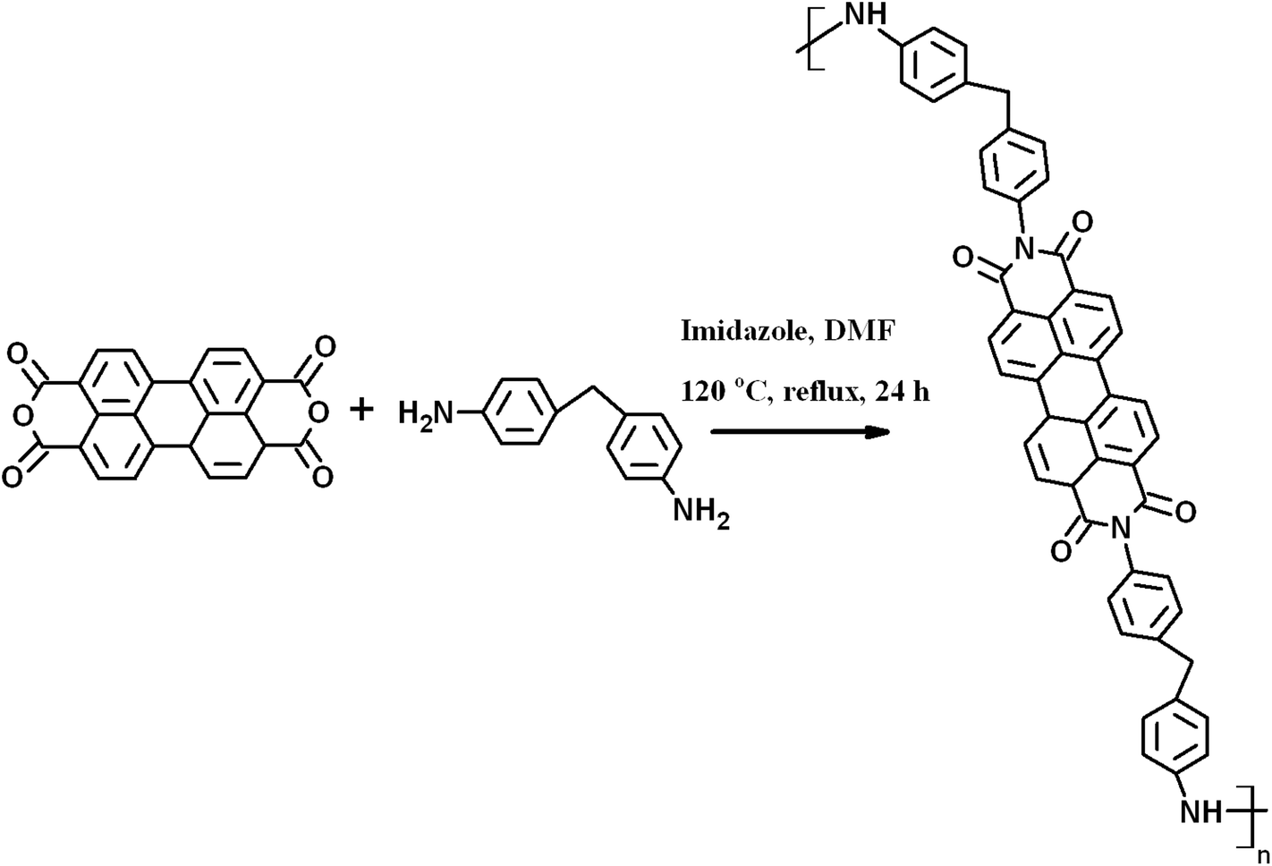
Synthesis of perylenediimide (PDI)
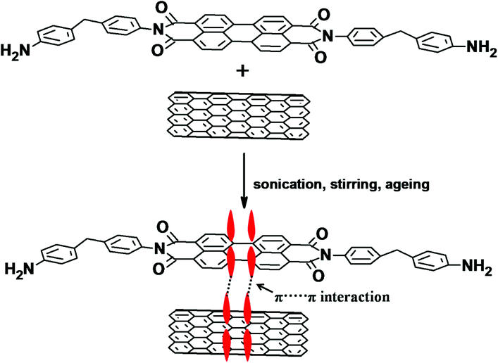
5 g of imidazole and 1 g of PTCD were mixed along with 2 g of MDA and a small amount of DMF in a round bottom flask and refluxed at 120 °C for 24 h in a N2 atmosphere. After completion, the reaction mixture was cooled to room temperature and the DMF was evaporated by vacuum drying. Subsequently, the solid mass was dissolved in chloroform and the organic layer was separated using a separation funnel after the addition of DI water. Finally, the chloroform was evaporated to yield perylenediimide (PDI), as shown in Scheme 1.
 |
| | Scheme 1 Synthesis of PDI. | |
Preparation of PDI-MWNT
MWNTs were modified with PDI by employing the following method. In a 250 ml beaker, 100 mg of MWNTs and 100 mg of as-synthesized PDI were dispersed in 100 ml of DMF and bath sonicated for 2 h. The mixture was then vigorously stirred at room temperature for 12 h and kept overnight for ageing. After 12 h, the unbound PDI was removed by centrifugation in DMF three times until the solution turned colourless and finally the solids were dried under vacuum at 80 °C. The π-skeleton of PDI makes it susceptible to π–π stacking with MWNTs. A cartoon further illustrating the possible π–π stacking between PDI and MWNTs is depicted in Scheme 2.
 |
| | Scheme 2 Preparation of PDI-MWNTs. | |
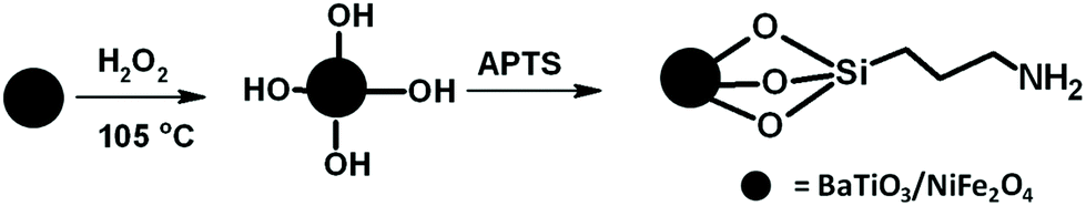
Preparation of 3-aminopropyltriethoxysilane (APTS)-coated nanoscopic BT and NF nanoparticles.
This is a two-step procedure where BT or NF nanoparticles were initially dispersed in H2O2 solution, followed by bath sonication for 30 min. The obtained mixture was then refluxed at 105 °C for 4 h. The hydroxylated BT or NF nanoparticles were then dried under vacuum at 100 °C. In the second step, as-prepared hydroxylated nanoparticles were mixed with APTS followed by refluxing at 80 °C under nitrogen atmosphere for 24 h. The mixture was then centrifuged and washed several times with toluene and dried under vacuum, finally yielding BT or NF terminated with NH2 functional moieties (Scheme 3).
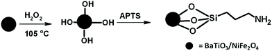 |
| | Scheme 3 Synthesis of amine-terminated nanoparticles. | |
Preparation of PC nanocomposites.
PC nanocomposites were prepared prior to their mixing with PVDF in the subsequent melt mixing step (will be discussed later). This strategy was adopted due to the following reasons. Most often sequential mixing is employed to restrict the nanoparticles in a preferred phase; however, in a small scale mixer like the one adopted here, such an approach often results in a poor dispersion of the phases as the energy of mixing is directly related to the volume filled in the barrel. In addition, this protocol was adopted to address two important concerns: (1) to study the migration of nanoparticles to their preferred phase and (2) to selectively position them in the PC phase in the blend structure. Initially, PC was dissolved in chloroform and later the different nanoscopic particles such as MWNTs, BT and NF were added to the PC solution and bath sonicated for 2 h before pouring the resultant mixture onto a Teflon coated Petri dish. The solvent was evaporated to obtain a sheet of PC nanocomposite. In the case of amine-terminated BT or NF nanoparticles, a similar protocol as mentioned above was followed except that the DMF solution was refluxed at 150 °C for 24 h. This was carried out for a specific purpose. The carbonyl groups of PC can undergo a nucleophilic substitution with the amine-terminated BT or NF nanoparticles. This results in chain scission of PC (as indicated in Scheme 4) and smaller PC grafts are attached on the surface of nanoparticles, as illustrated in Scheme 4.
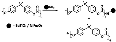 |
| | Scheme 4 Probable reaction between PC and amine-terminated nanoparticles. | |
Blend preparation.
Neat blends of PC/PVDF (50/50) (w/w) without and with different nanoparticles were processed by melt mixing using a Haake minilab-II melt compounder under a N2 atmosphere at 260 °C at 60 rpm for 20 min. As mentioned above, the PDI-MWNTs thus prepared (Scheme 1) were also added directly into the mixer and processed under the same extrusion conditions. In addition, few compositions were prepared where BT or NF nanoparticles were directly mixed along with the blend components and under the same extrusion condition. In order to restrict the migration of nanoparticles to their preferred phase (here PVDF) during mixing, we adopted a two-step mixing procedure for a few compositions, as discussed above. The PC nanocomposites, which were prepared following the earlier steps, were melt mixed with PVDF and PDI-MWNTs under the same extrusion conditions except that the mixing time was set at 10 min. Before processing all the samples were pre-dried for 24 h at 80 °C in a vacuum oven. Melt mixed extruded samples were subsequently compression molded at 260 °C using a lab scale hydraulic press into specific shapes for different tests.
Characterizations
Fourier transform infrared (FT-IR) spectroscopy was carried out using KBr pellets with a Perkin-Elmer GX in the range of 4000–400 cm−1 using a resolution of 4 cm−1. Morphological analyses for various blends were assessed using an ULTRA 55 scanning electron microscope (SEM) at an accelerating voltage of 10 kV, which is also attached with a EDS detector where the accelerating voltage is 15 kV. Transmission electron microscopy (TEM) images were acquired using Tecnai G2F30 at 300 kV. The flow characteristics of the blends were assessed using a DHR-3 rheometer from TA instruments using parallel plate geometry (25 mm in diameter). To prevent any degradation, all the tests were performed under a nitrogen atmosphere. The samples were vacuum dried at 80 °C before the rheological measurements.
Room temperature electrical conductivity of the blends was studied using an Alpha-N Analyser, Novocontrol (Germany) in a frequency range from 0.1 Hz to 10 MHz. Uniformly polished compression-molded disks were used as specimens and electrical conductivity was measured across the thickness. The EMI shielding characteristics was studied in the X and Ku-band frequency range using a Anritsu MS4642A vector network analyser (VNA) coupled to a coax (Damaskos M07T) set up. The set up was calibrated by SOLT (short-open-load-transmission) for both the ports, simultaneously. Toroidal specimens 5 mm thick, which were obtained by compression molding, were used to evaluate the S parameters (S11, S12, S22 and S21) in a wide range of frequency.
Results and discussion
Synthesis and characterization of PDI-MWNT, BT-NH2 and NF-NH2
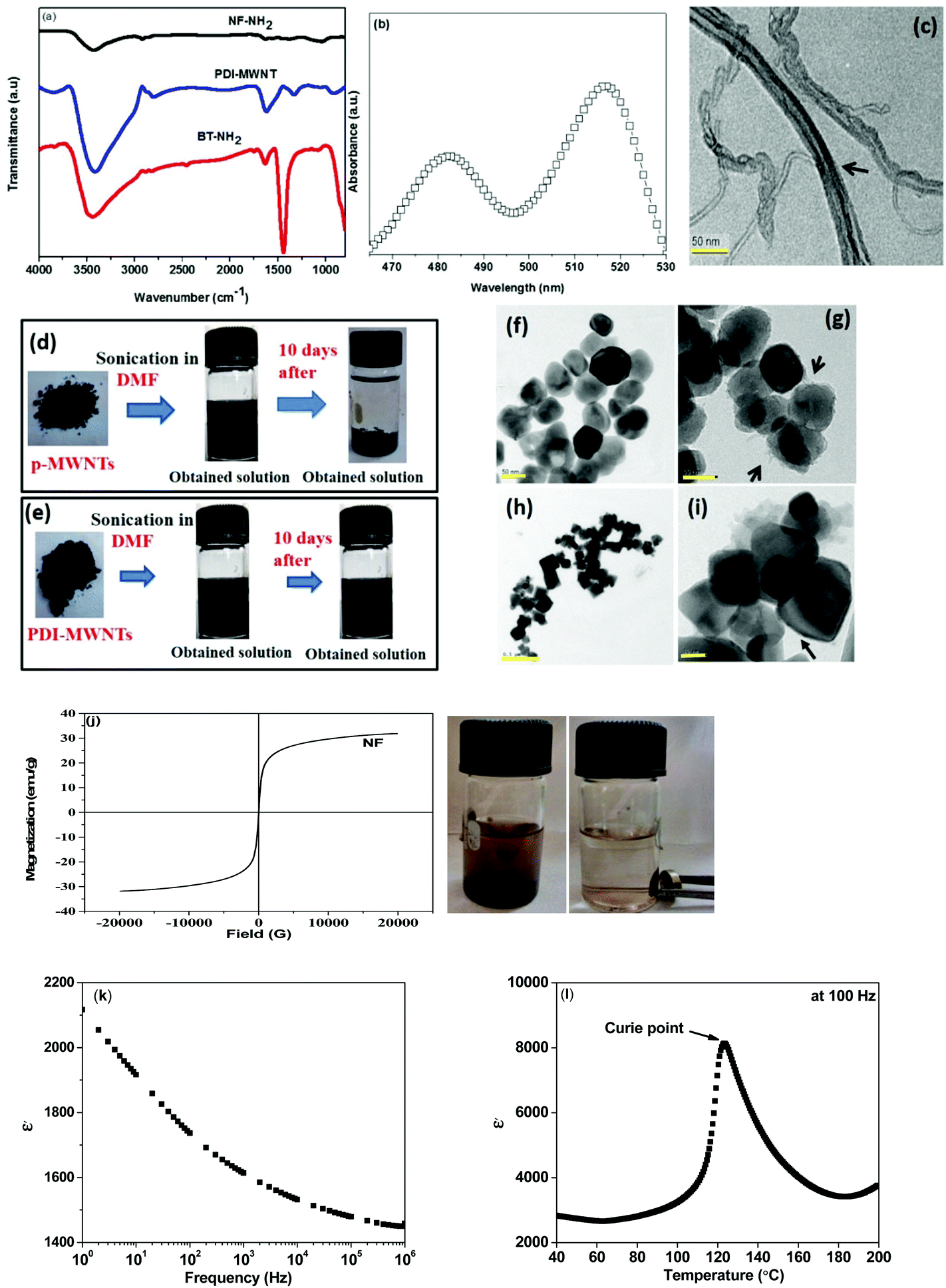
The chemical functionalization of MWNTs can result in substantial damage to the integrity of the nanotubes. By employing a facile physisorption-based modification, like the one adopted here, it is possible to obtain well dispersed MWNTs in the blends as the perylene moiety interacts with the MWNTs via π–π stacking and reduces the van der Waals interactions between the nanotubes. It is envisaged that π–π stacking is stronger than other non-covalent interactions such as van der Waals force of attraction. The synthesis of PDI-MWNTs is illustrated schematically in Scheme 1 and the details are explained in the Experimental section. Fig. 1a shows the FT-IR spectra of PDI-MWNT, BT-NH2 and NF-NH2. The peak at 3415 cm−1 indicates the N–H stretching frequency, which is originated from PDI moieties. The peak at 1621 cm−1 indicates the amidation reaction between MDA and PTCD. However, as the amine group of MDA is highly reactive towards the anhydride groups of PTCD, there could be a possibility of the formation of coordinating polymer network of PDI.30 In the case of BT-NH2 and NF-NH2, the broad peak at 3441 cm−1 indicates the N–H stretching frequency due to the presence of APTS. Peak at 1634 cm−1 also indicate the N–H bending frequency and the peak at 1442 cm−1 indicates the C–O binding to Ti ions in the case of BT nanoparticles. UV-vis absorption experiments were carried out to explore the photophysical properties and charge transfer interactions of PDI-MWNT. As shown in Fig. 1b, there are two strong absorption peaks at 485 and 520 nm, which clearly manifest the successful binding of PDI molecules on MWNTs. The absorption spectrum of PDI normally shows three pronounced peaks (in the range of 450–525 nm) and a shoulder around 425 nm, which correspond to the 0–0, 0–1, 0–2, and 0–3 electronic transitions. These peaks originate from the π–π* charge transition in perylene core molecules, which are slightly red shifted due to the interaction with MWNTs. Furthermore, from the TEM image (Fig. 1c) it is also observed that PDI molecules are attached on the surface of MWNTs. Further evidence on the quality of dispersion comes from the state of dispersion in polar solvents (Fig. 1d–e). The required quantity of p-MWNTs was dispersed in DMF by bath sonication, but after a few hours, the p-MWNTs settle at the bottom of the vial. However, interestingly in the case of PDI-MWNTs a stable dispersion was observed several weeks after the initial sonication process. This clearly manifests the key role of PDI in rendering a uniform dispersion of MWNTs. The TEM micrographs of BT (BT-NH2) and NF (NF-NH2) are displayed in Fig. 1f–i. The attachment of amine-terminated APTS molecules is observed in the TEM images and are indicated by arrows. Fig. 1h illustrates the magnetization hysteresis of NF nanoparticles. From the hysteresis loop, it can be inferred that the observed saturation magnetization (Ms) is ca. 31 emu g−1 and the remnant magnetization (MR) is 0.3 emu g−1. The coercivity (HC) is observed to be ca. 10.4 Oe. The inset of Fig. 1j clearly demonstrates the magnetic nature of NF-NH2 particles. Furthermore, we have characterized the BT nanoparticles. The dielectric constant as a function of frequency at room temperature is shown in Fig. 1k and the Curie temperature as inferred from the variation in the dielectric constant as a function of temperature is illustrated in Fig. 1l. At room temperature, BT adopts a tetragonal perovskite type structure and is ferroelectric. It transforms to a cubic (paraelectric) structure at the Curie temperature. The spontaneous polarization of BT is ca. 0.15 C m−2 at room temperature and this together with high dielectric loss in the GHz frequency makes it a potential candidate as a microwave absorber.
 |
| | Fig. 1 (a) FT-IR of various synthesized materials. (b) UV-Vis spectrum of PDI-MWNT. (c) TEM micrograph of PDI-MWNT. (d–e) State of dispersion of p-MWNT and PDI-MWNT in DMF. TEM micrographs of (f) BT, (g) BT-NH2, (h) NF and (i) NF-NH2. (j) Magnetization hysteresis of NF nanoparticles (inset of 1j demonstrates the magnetic nature of NF-NH2 nanoparticles as observed in the vial on to the right; the vial to the left shows the dispersion of NF-NH2 in acetone). (k) Dielectric constant of BT as a function of frequency at room temperature. (l) Dielectric constant of BT as a function of temperature at 100 Hz frequency showing the Curie temperature. (The scale bar is 50 nm in the TEM micrographs). | |
Selective localization, phase morphology and the state of dispersion: SEM and EDS
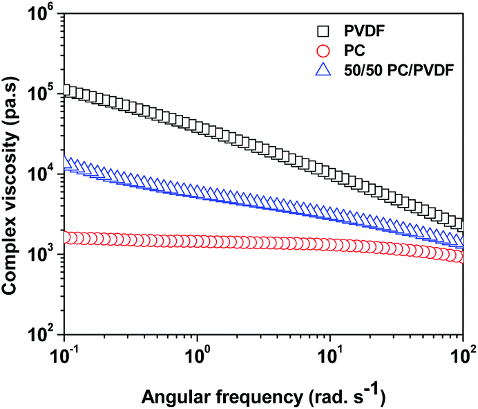
The precise control of nanoparticles localization in blend structures is a key parameter that dictates the final properties of immiscible systems. It is important to understand the factors that govern the migration/localization of the nanoparticles in the blends. From the classical thermodynamic point of view, the selective localization of MWNTs can be predicted with the help of temperature dependent surface free energies of the constituents. The high surface energy of PC (26 mJ m−2) in contrast to PVDF (19.52 mJ m−2) suggests that the nanoparticles might migrate to the PC phase. However, we observed that the MWNTs are localized in the PVDF phase. Next to this criterion, it is often observed that the nanoscopic particles localize in the less viscous phase as their diffusion to the other phase is limited by the viscous medium. The complex viscosity (Fig. 2) of the constituents suggests that the MWNTs might prefer to localize in the lower viscous phase (here PC). To our surprise, the MWNTs were localized in the PVDF phase against both the thermodynamic and the viscosity predictions. This strongly suggests that MWNTs have preferential affinity towards the PVDF phase in the blends and can be understood because of the higher polarity of the PVDF phase over PC, as can be seen from Table 1. In our previous study,5 we observed similar effects where MWNTs were preferentially localized in the PVDF phase even when they were blended with a lower viscosity and higher surface free energy component (ABS). The SEM micrographs of selective dissolution experiments further support the fact that MWNTs are localized in the PVDF phase.
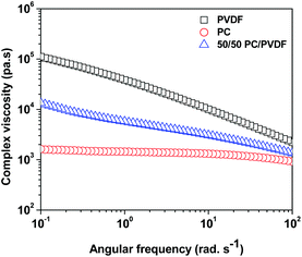 |
| | Fig. 2 Complex viscosity of constituent polymers at 260 °C as a function of frequency. | |
Table 1 Surface free energy and polarity of constituents at 260 °C
| Constituents |
Surface free energy (mJ m−2) |
Polarity (%) |
| PVDF |
19.52 |
38 |
| PC |
26 |
30.5 |
| MWNTs |
45.336 |
59 |
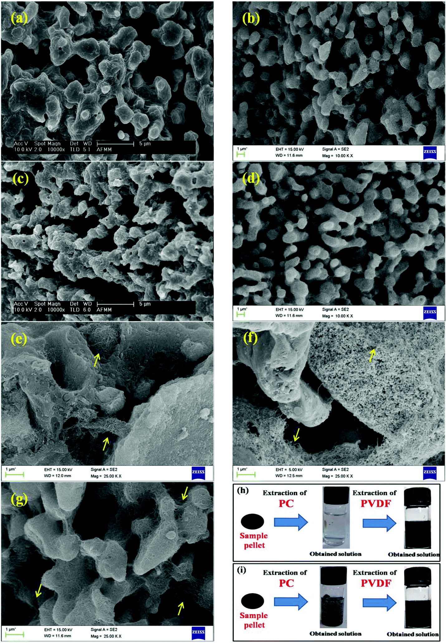
Fig. 3 shows the SEM micrographs of various 50/50 PC/PVDF blends. For the SEM analysis, cryofractured extruded strands were used and etched in chloroform for 72 h to remove the PC phase, prior to the measurements. This was done to improve the contrast between the phases. Hence, the voids in the SEM micrographs represent the etched out PC phase. Fig. 3a and b shows the SEM micrographs of the neat 50/50 PC/PVDF blends with MWNTs. Both the blends exhibit a co-continuous type of microstructure. As briefly mentioned above, the higher magnification images reveal that the MWNTs are selectively localized in the PVDF phase, as indicated in Fig. 3c. Interestingly, MWNTs were observed in the continuous PVDF phase even when they were initially mixed with PC followed by PVDF. This phenomenon clearly indicates that MWNTs migrated to the PVDF phase in situ during melt mixing. The SEM micrographs of the blends with PDI-MWNTs also revealed co-continuous structures, and as expected, the modified nanotubes were localized in the PVDF phase of the blends. One interesting fact that can be appreciated here is that the PDI-MWNTs are exfoliated and a finer mesh-like structure is visualized in the remaining PVDF phase. Furthermore, by selective dissolution experiments we can ascertain the localization of various nanoparticles in the blends. As shown in Fig. 3h, after the extraction of PC phase by chloroform, the obtained solution is colorless; however, after the extraction of PVDF by DMF, the obtained solution is black, which clearly indicates that when MWNTs were directly added into the extruder, they were selectively located in PVDF phase. However, from Fig. 3i, it is clear that when PC-MWNT composites were melt mixed with PVDF, the MWNTs migrated towards the PVDF phase, manifesting a dark colored solution in both the phases. This can have positive consequences with respect to the charge transport in the blends and will be discussed later on.
 |
| | Fig. 3 SEM micrograph of (a) neat 50/50 PC/PVDF (b) with 3 wt% p-MWNT in PVDF phase (c) with 3 wt% p-MWNT in both phase (d) with 3 wt% PDI-MWNT in PVDF phase, high resolution of SEM micrographs of (e) neat 50/50 PC/PVDF (f) with 3 wt% p-MWNT in PVDF phase (g) with 3 wt% PDI-MWNT in PVDF phase, selective dissolution experiments PC phase is extracted by chloroform and PVDF phase is by DMF (h) with 3 wt% p-MWNT in PVDF phase (i) with 3 wt% p-MWNT in both phase. | |
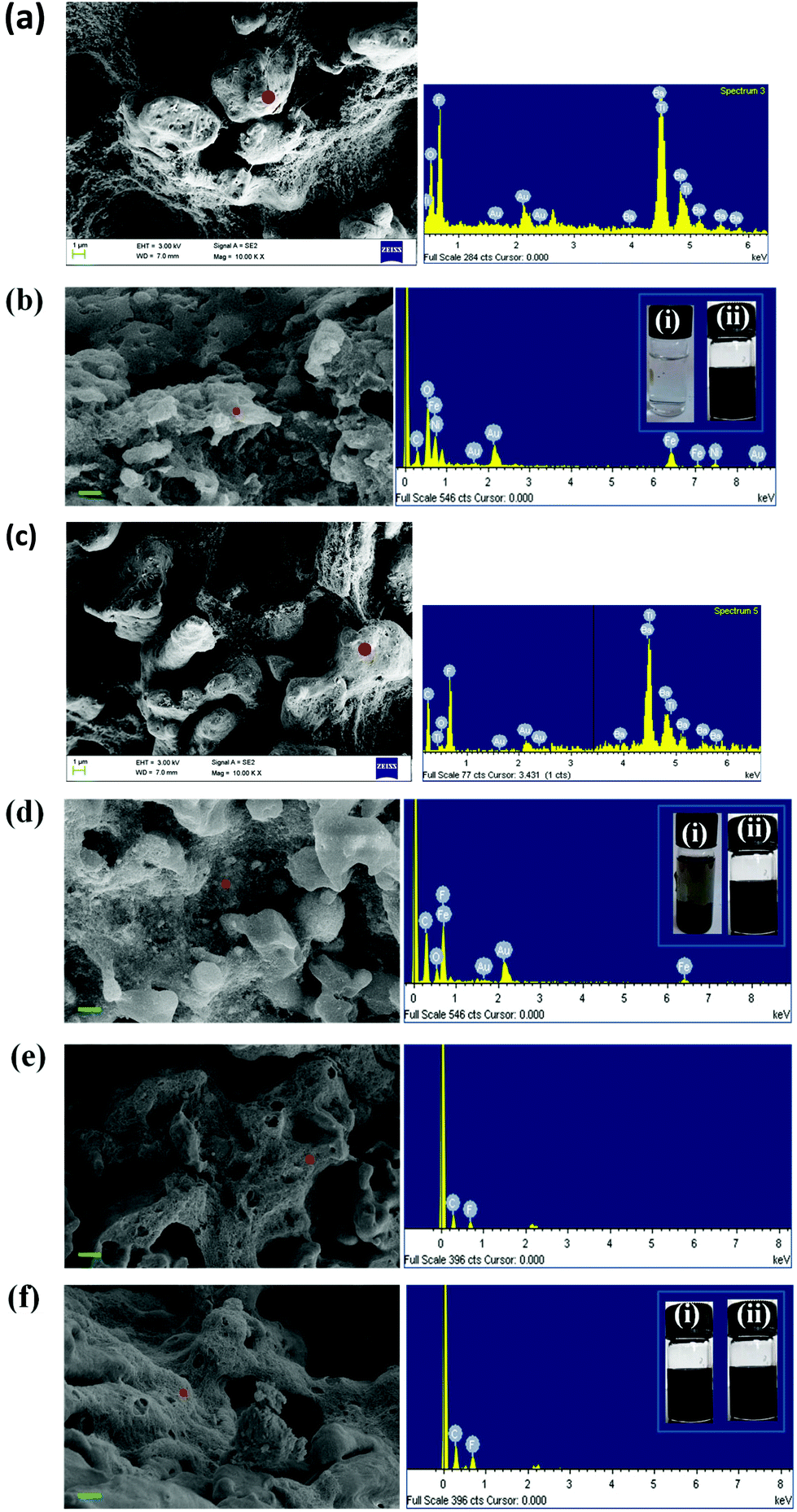
As observed from the previous section, MWNTs are localized selectively in the PVDF phase irrespective of the mixing protocol adopted during the preparation of the blends. Hence, in the following section we focus only on the precise location of the BT and NF nanoparticles using SEM, EDS and selective dissolution experiments as the included conductive material (MWNTs) is intended to be localized in the PVDF phase. As expected, the BT and the NF nanoparticles migrated to the PVDF phase during melt mixing, when all the components were mixed together. This is supported by EDS collected from the cryofractured and PC-etched samples and further confirmed by selectively dissolving the phases in respective solvents (chloroform for PC and DMF for PVDF). The EDS analysis of the blends revealed the presence of BT or NF in both the phases when they were initially mixed with PC followed by PVDF and only in PVDF when mixed all together. This strongly suggests that the nanoparticles have strong affinity towards the PVDF phase as driven by polarity. This was further supported by selective dissolution experiments (insets of Fig. 3h–i). For instance, in the blends when all the constitutents were mixed together, the EDS analysis supported the presence of BT or NF in the PVDF phase (Fig. 4a and b), as expected. Now, when PC nanocomposites with either BT or NF are mixed with PVDF (and PDI-MWNTs), the EDS analysis revealed the presence of BT or NF in the remaining PVDF phase, though only a weak signal could be captured. This possibly could explain the migration of nanoparticles from PC to PVDF during mixing, as also supported by selective dissolution experiments (inset of Fig. 4c and d). Interestingly, when PC nanocomposites with amine-terminated BT or NF nanoparticles were mixed with PVDF, we did not observe any signal of either BT or NF in the PVDF phase as manifested from the EDS collected from the remaining PVDF phase (Fig. 4e and f). This strongly suggests that BT or NF is localized in the PC phase due to nucleophilic substitution reaction with PC as discussed above and is also supported by the selective dissolution experiments (inset of Fig. 4f). Hence, surface active groups can facilitate ordered arrangement of the nanoscopic particles in the blend structure.
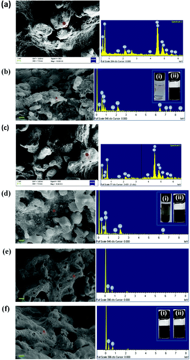 |
| | Fig. 4 EDS spectra of PC/PVDF blends containing 3 wt% PDI-MWNT in PVDF phase along with (a) BT in PVDF phase, (b) NF in PVDF phase, (c) BT in both phase, (d) NF in both phase, (e) BT in PC phase and (f) NF in PC phase. The insets of Fig. (b), (d), and (f) show the selective dissolution of blends where the vial (i) indicates extracted PC solution with chloroform and vial (ii) indicates extracted PVDF solution by DMF (the red dot in the SEM micrographs indicate the area from which the EDS spectra were acquired and the scale bar of the different micrographs is 1 μm). | |
Interconnected network like structure of MWNTs facilitated by electron acceptor molecules
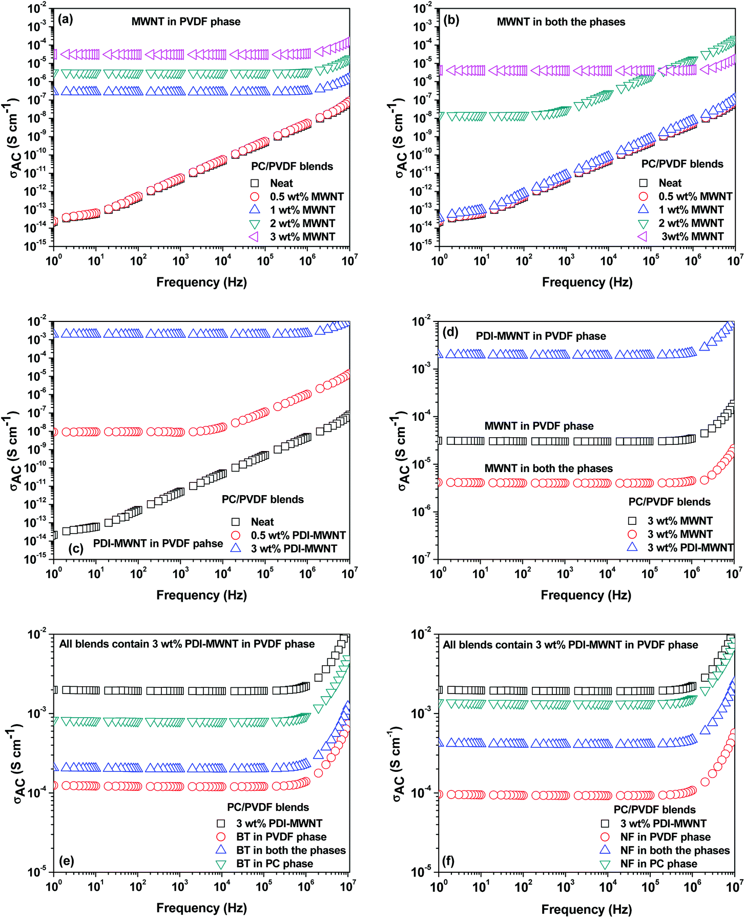
The continuous conducting network of particles is a key factor for improving electrical conductivity in polymeric systems. In general, electrical conductivity depends on size, shape, concentration, distribution, and surface treatment of the included conductive material. In this context, the aspect ratio of the particles plays an important role in deciding the electrical percolation threshold. Most often, the surface functionalization by covalent treatment reduces the overall electrical conductivity in MWNT-based nanocomposites. Alternatively, grafting polymeric chains or even wrapping MWNTs can also impede the geometrical contact between the nanotubes. Fig. 5a shows the AC electrical conductivity in the blends with varying concentration of MWNTs (0–3 wt%), where the MWNTs are selectively dispersed in the PVDF phase. It is evident that the conductivity of the blend scales with the MWNTs and the percolation threshold is between 0.5 and 1 wt%. This clearly indicates that the distance between two nanotubes decreases with increasing concentration, thereby allowing the formation of a three-dimensional network-like structure in the blend. This further helps in efficient charge transport through tunnelling or hopping. When the MWNTs migrate to the PVDF phase during mixing, the overall electrical conductivity drops due to the lack of an interconnecting network like formation of MWNTs in a given phase. Hence, the percolation threshold lies between 1 and 2 wt% in the blends (Fig. 5b).The modification of MWNTs with PDI was intended to facilitate better dispersion and more efficient charge transport. This further resulted in higher electrical conductivity in the blends, as shown in Fig. 5c and d. For instance, PDI-MWNT showed a two-order increment in AC conductivity at 3 wt% and in addition, the percolation threshold was in between 0 and 0.5 wt%, in contrast to 0.5–1 wt% in the case of unmodified MWNTs. This clearly indicates that due to π–π stacking of electron acceptor perylene molecules with the side wall of MWNTs, the free electron can tunnel through the network of PDI-MWNT. The inclusion of BT or NF in the PVDF phase results in a decrease in the overall electrical conductivity. It is envisaged that when BT or NF particles migrate from PC to PVDF or when they are exclusively localized in the PVDF phase, they interfere with the interconnected network-like structure of PDI-MWNTs and increases resistance due to the formation of a capacitor-resistor type of network. However, this phenomenon was more pronounced when BT or NF particles were exclusively located in the PVDF phase rather than when they migrated from PC. This is further manifested in the electrical conductivity measurements. In order to get more insight into the mechanism of charge transport, the AC electrical conductivity curves were fitted with a power law (σAC(ω) = σDC + Aωn where σDC and ω are DC conductivity and the angular frequency, respectively). Here, the ‘n’ is an exponent ranging from 0–1 and is a function of both temperature and frequency. The exponent ‘n’ varies with the inclusion of BT or NF nanoparticles along with the PDI-MWNTs. The blend with 3 wt% MWNT in the PVDF phase exhibits n = 0.82, hence manifesting in a three dimensional network of capacitors and resistors where the charge transport is dominated by hopping. In the presence of PDI-MWNT, the exponent is 0.66, which indicates that the charge transport mainly occurs by tunneling through a 3D network of PDI-MWNT in the PVDF phase. Interestingly it is envisaged that when BT or NF particles migrate from PC to PVDF or when they are exclusively localized in the PVDF phase, they interfere with the interconnected network-like structure of PDI-MWNTs. However, this phenomenon was more pronounced when BT or NF particles were exclusively located in the PVDF phase rather than when they migrated from PC, which we discussed earlier. The value of exponent ‘n’ increases with the inclusion of BT or NF nanoparticles in the PVDF phase and alters the charge transport mechanism from tunneling to hopping. Interestingly, by adopting this compartmentalized approach, the exponent ‘n’ is ca. 0.7, which strongly suggests that the charge transport is primarily by tunneling, as illustrated schematically in Fig. 5. A cartoon further illustrating the effect of BT/NF on the interconnected network-like structure of PDI-MWNTs in different blend structures is shown in Fig. 6.
 |
| | Fig. 5 Room temperature AC conductivity plot as a function of frequency of (a) p-MWNTs in PVDF phase, (b) p-MWNTs in both phases, (c) PDI-MWNTs in PVDF phase, (d) comparisons between p-MWNTs and PDI-MWNTs, (e) BT containing blends and (f) NF-containing blends. | |
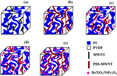 |
| | Fig. 6 Electron transfer mechanisms of blends (a) with 3 wt% p-MWNT, (b) with 3 wt% PDI-MWNT, (c) with nanoparticles in PVDF phase, (d) with nanoparticles in both phase and (e) with nanoparticles in PC phase. | |
Attenuation of EM radiation: effect of MWNT, barium titanate and nickel ferrite
It is envisaged that by controlling microstructural heterogeneities in the composites, unique absorption responses at macroscale can be achieved. This is related to the interaction between the incident EM waves with the composite as the EM waves come across a variety of microscopic boundaries due to the inclusions.
The total shield effectiveness (SET) is expressed in terms of shielding by absorption (SEA), by reflection (SER) and multiple reflections (SEMR). It is generally agreed upon that if the shield thickness is greater than the skin depth (explained below), the multiple reflections can be neglected because the reflected wave from the internal surface will be absorbed by the conductive materials. The total shielding effectiveness can be expressed as22
| | | SET = SEA + SER (when, SET > 15 dB) | (1) |
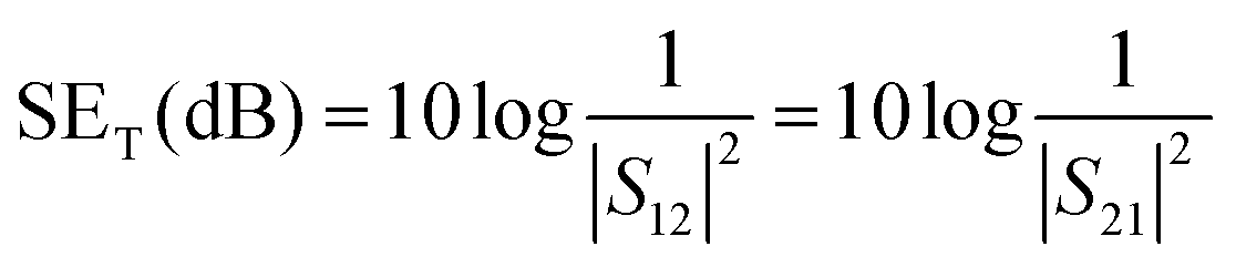
In a vector network analyser, the EMI SE is represented in terms of scattering parameters (S11, S12, and S21) and hence, SET can be expressed by the following expression,
| | 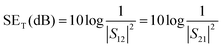 | (2) |
where scattering parameters
S11 is the forward reflection coefficient,
S12 is the reverse transmission coefficient and
S21 is the forward transmission coefficient obtained from VNA.
We can evaluate the reflection and the absorption parameters by knowing the scattering parameters with the help of following equations,22
| | | SER = 10 × log10(1/(1 − S112)) | (3) |
| | | SEA = 10 × log10((1 − S112)/S122) | (4) |
The skin depth (δ) is the intensity of penetration into the conductive material at which generally the electric field drops to 1/e, which roughly means that the energy of EM radiation is reduced to 33% of its original strength. The skin depth depends on the material's property as described by the following expression,31,32
| |  | (5) |
where
μ is the permittivity,
σ is the conductivity of the blend and
f is the frequency in Hz. The absorption is related to the skin depth as,
32where
t is the thickness of the samples in mm. Here, the scattering parameters were acquired in a broad range of frequency: X (8–12 GHz) and K
u-band (12–18 GHz).
While the neat blends are transparent to EM radiation, the SET is observed to increase with increasing MWNT content in the blends (Fig. 7). It is envisaged that in MWNT-based composites, with an increasing concentration of MWNTs, the dielectric losses are higher due to wave reflection rather than absorption. The MWNTs when exclusively localized in the PVDF phase showed better shielding effectiveness than when they were localized in both the phases on account of their migration from PC to PVDF. This is also supported by the observed lower electrical conductivity in the blends as discussed earlier. The blends with PDI-MWNT resulted in a higher SET. As we discussed earlier, beyond the percolation threshold the interconnected conducting network can easily carry mobile charge and hence attenuate EM radiation by reflection. From Fig. 7a–e, we understand that in the presence of PDI-MWNTs, the finer mesh of MWNTs facilitated the conduction of more free electrons, which eventually helped in reflecting the incident EM waves. In addition, finer mesh-like structure of CNTs can also facilitate multiple scattering inside the network due to their large specific surface area. Because MWNTs are non-magnetic, the absorption mainly arises from polarization, ohmic losses and multiple scattering. The latter effect is more pronounced in the case of PDI-MWNTs and hence the overall SE is higher than in the blends with MWNTs.
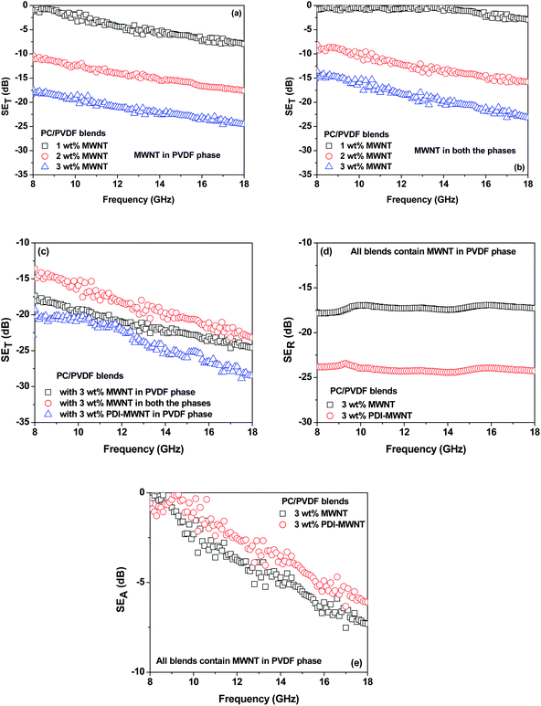 |
| | Fig. 7 Total shielding effectiveness as a function of frequency plot (a) p-MWNTs in PVDF phase, (b) p-MWNTs in both the phases, (c) comparisons between PDI-MWNTs and p-MWNTs in different phases, comparisons of (d) reflection parameters and (e) absorption parameters as a function of frequency between p-MWNTs and PDI-MWNTs. | |
However, the inclusion of BT or NF nanoparticles in the blend alters not only the distribution of MWNTs in the blends but also alters the mechanism of shielding. Microwave radiation, when incident on a lossy dispersive material, creates heat as it interacts with the material's molecular and electronic structure. Hence, heterogeneous inclusions within an effective medium approach are described by two material parameters; the complex (relative) permittivity (ε = ε′ − jε′′) and the magnetic permeability (μ = μ′ − jμ′′). The ε′′ (or μ′′) are associated with dielectric loss or energy dissipation within a material resulting from conduction, resonance, and relaxation mechanisms. In the following section, we will discuss the effect of nanostructure ordering with different materials characteristics on the absorption of EM radiations.
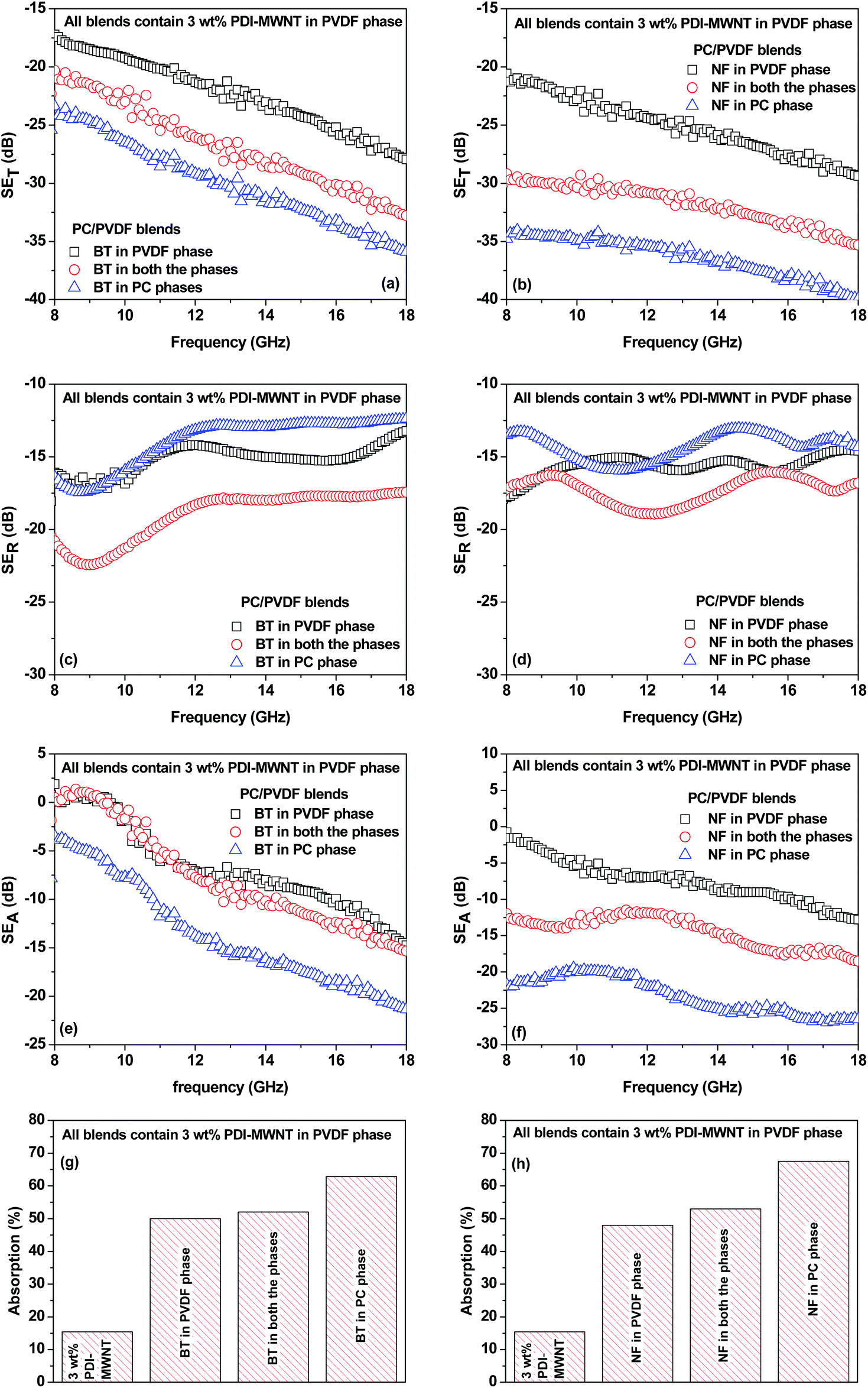
With the inclusion of BT or NF nanoparticles in the blend, the SET improved significantly as reflected in Fig. 8a–h. It is clear that when BT or NF nanoparticles are exclusively located in the PVDF phase or when they are in both the phases, the change in SET is not appreciable. However; the absorption is significantly altered with respect to the blends with MWNTs. One possible explanation could be that such inclusions can interfere with the interconnected network of MWNTs, resulting in a decrease in the overall conductivity of the blends. This is also supported by the fact that the reflection decreased and the absorption increased. The latter is due to the presence of both electric and/or magnetic dipoles. Interestingly, by this compartmentalized approach, where BT or NF nanoparticles exclusively locate in the PC phase and the conductive material locates in PVDF, the overall SET increased significantly, demonstrating the synergetic effect from both the phases which contain nanoscopic particles of different characteristics. Hence, when the EM radiation interacts with such shields, the resulting local field variations can have a strong effect on the energy absorption at such boundaries as the absorption depends quadratically on the electric field intensity.
 |
| | Fig. 8 Total shielding effectiveness as a function of frequency for (a) BT-containing blends and (b) NF-containing blends. Reflection parameters as a function of frequency for (c) BT-containing blends and (d) NF-containing blends. Absorption parameters as a function of frequency for (e) BT-containing blends and (f) NF-containing blends. Percent absorption for (g) BT-containing blends and (h) NF-containing blends. | |
Now in order to get more insight into the mechanism of shielding, which also establishes the correlation between the observed shielding response and electromagnetic attributes, we took a closer look at the relative complex permittivity and permeability values. Well-established Nicolson and Ross line theory was used to estimate the permittivity and permeability values from the scattering parameters. The relative complex permittivity is depicted in Fig. 9a and b as a function of frequency in the range of 8–20 GHz for various blends. It is observed that blends with PDI-MWNTs showed higher relative complex permittivities than MWNTs. As the relative complex permittivity is a measure of the polarizability of the material, it is evident that on interacting with EM waves the dipolar and electric polarizations are enhanced in the case of PDI-MWNTs. In addition, blends with MWNTs had lower complex permittivities as compared to the blends with lossy inclusions. This is because in heterogeneous dielectrics, the accumulation of virtual charges at the interface of two media having different dielectric constants and conductivities lead to interfacial polarization, known as Maxwell–Wagner polarization. Interestingly, the complex permittivity also changed in the compartmentalized approach. The maximum complex permittivity is observed when the BT or NF inclusions are in the PC phase and PDI-MWNT in PVDF. Furthermore, we observed that the presence of BT or NF in PVDF decreased the overall conductivity of the blends as the inclusions interfere with the conducting network and increase the contact resistance between the neighboring MWNTs. Therefore, it is reasonable to observe a decrease in the relative complex permittivity. By fitting the power law equation, the value of the exponent ‘n’, which is a representative of resistance and capacitance behavior of the blend, suggests that the PDI-MWNTs represent an equivalent network of 66% resistor-34% capacitor. In the presence of BT or NF in PVDF, the value of the exponent ‘n’ is >0.80, which suggests charge transport by hopping. Interestingly, by this compartmentalized approach, wherein BT or NF nanoparticles exclusively locate in the PC phase and the interconnected MWNTs in the PVDF phase, the value of exponent is <0.7, which suggests charge transport by tunnelling. The external electromagnetic fields interact with the composite material, and this indicates that the EM waves overcome a variety of boundary conditions due to the compartmentalized inclusion approach for making the heterostructure. The resulting local field variations can have a very strong effect on energy absorption at such boundaries because absorption depends quadratically on the electric field intensity (Table 2).
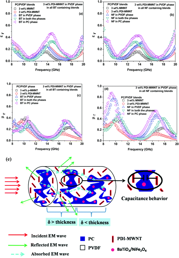 |
| | Fig. 9 Relative complex permittivity plots of (a) high dielectric constant materials and (b) ferromagnetic materials. Relative complex permeability plots of (c) high dielectric constant materials and (d) ferromagnetic materials. (e) A cartoon illustrating the mechanism of shielding in a toroidal sample. | |
Table 2 Different parameters derived from power law equation
| Compositions |
σ
DC (s cm−1) |
ω (Hz) |
n
|
| 3 wt% MWNT in PVDF phase |
3.1 × 10⁻⁵ |
8.2 × 10⁻⁶ |
0.82 |
| 3 wt% PDI-MWNT in PVDF phase |
2 × 10⁻³ |
9.4 × 10⁻⁵ |
0.66 |
| BT in PVDF phase |
1.2 × 10⁻⁴ |
9.4 × 10⁻⁶ |
0.80 |
| BT in both the phases |
2 × 10⁻⁴ |
2.7 × 10⁻⁵ |
0.74 |
| BT-NH2 in PC phase |
8 × 10⁻⁴ |
8.0 × 10⁻⁵ |
0.61 |
| NF in PVDF phase |
9.8 × 10⁻⁵ |
9.0 × 10⁻⁶ |
0.78 |
| NF in both the phases |
4 × 10⁻⁴ |
2.1 × 10⁻⁵ |
0.73 |
| NF-NH2 in PC phase |
1.3 × 10⁻³ |
8.3 × 10⁻⁵ |
0.60 |
In Fig. 9c and d, the relative complex permeabilities of blend are depicted. The relative complex permeabilities of the blends increased with the addition of magnetic nanoparticles (NF). Interestingly, the relative complex permeability was also enhanced due to this compartmentalized approach. These results clearly indicate that localizing magnetic particles in one of the phases leads to a more effective increase in permeability values than when they are in both the phases even though the role of magnetic properties have great influence on the relative complex permeability in the MHz frequency region rather than the GHz region.
As we discussed earlier for conductive materials, when σ ≫ ωε where σ is the conductivity and ω is the angular frequency of radiation and ε is the relative permittivity then,33
where
f is the frequency in Hz,
μ is the permeability (
μ =
μ0μr) and conductivity
σ = 2π
fε0ε′′. The shielding by absorption increases with the increasing values of
μr and
εr. Moreover, the increment in relative complex permittivity and permeability values result in higher absorption of the incident EM waves. The gaps between the conducting MWNTs act as micro/nano-capacitors in the blends. This results in an increase in the dielectric constant in the blends. As each of the phases is filled with materials with different characteristics, the effect is more prominent in this compartmentalized approach in contrast to when the nanoscopic particles were localized in the same phase. The charge accumulation on the surface of BT/NF nanoparticles can also increase the dielectric constant in the blends. It is envisaged that surface reflection is not good for absorption, and with weak impedance matching, the EM waves cannot effectively enter the sample. By filling bi-continuous blends with particles that show either high dielectric loss in the GHz frequency (BT) or high magnetic loss (NF), the attenuation can be enhanced. In
Fig. 9e, we schematically represent the shielding mechanism of a toroidal sample designed
via this compartmentalized approach (
Table 3).
Table 3 Different shielding parameters of various samples at a frequency of 18 GHz
| Composition |
SET (dB) |
SEA (dB) |
SER (dB) |
| With 3 wt% MWNT in PVDF phase |
−24.5 |
−7 |
−17.5 |
| With 3 wt% MWNT in PC + PVDF phase |
−23 |
−7 |
−16 |
| With 3 wt% PDI-MWNT in PVDF phase |
−28.5 |
−4.4 |
−24.1 |
| BT in PVDF phase |
−29 |
−14.6 |
−14.4 |
| NF in PVDF phase |
−29 |
−14 |
−15 |
| BT in both the phases |
−33 |
−17 |
−16 |
| NF in both the phases |
−35.5 |
−18.5 |
−17 |
| BT-NH2 in PC phase |
−35 |
−22 |
−13 |
| NF-NH2 in PC phase |
−40 |
−27 |
−13 |
Furthermore, the concept of the compartmentalized approach is evident from the reflection loss which is expressed as,34
| | | RL = 20 × log(|Zin − 1|/|Zin + 1| | (7) |
| |  | (8) |
where
c is the velocity of light and
t is the thickness of the samples.
From Fig. 10a we can see that in the presence of a conductive material (PDI-MWNT) in the PVDF, the RL has changed from −10 dB to −14 dB at 18 GHz frequency. But as MWNTs are nonmagnetic materials, reflection loss is generated either from polarization, ohmic losses or by multiple reflections, as discussed earlier. Furthermore, PDI-MWNTs have higher relative complex permittivity, which helps in higher reflection loss parameters due to dielectric relaxation. From Fig. 10b and c, when BT or NF nanoparticles are exclusively positioned in the PC phase, maximum RL in the Ku band results rather than when such inclusions are positioned in the PVDF phase or migrate from PC phase. This is consistent with the relative complex permittivity and permeability values. The blends with NF nanoparticles exhibited excellent reflection loss due to combined contribution of dielectric and magnetic losses. It is well understood that the thickness of the samples is one of the essential factors that determines the total shielding effectiveness and the band width in reflection loss curves. Therefore, we varied the thickness of the sample that showed the highest attenuation from 1 mm to 5 mm. Fig. 10d, clearly depicted that the reflection loss peaks are shifted from higher to lower frequencies with increasing thickness, concomitant with quarter-wavelength attenuation (Table 4).
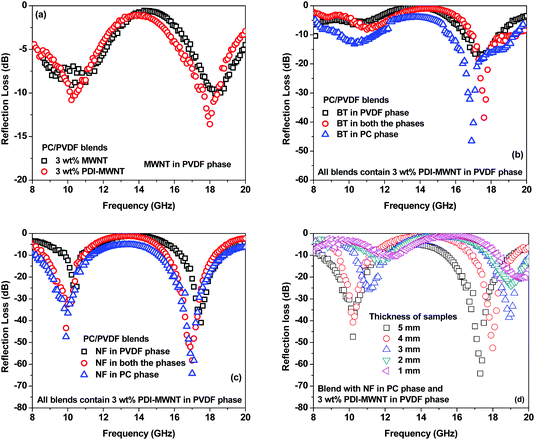 |
| | Fig. 10 Reflection loss as a function of frequency for (a) blend with different MWNTs, (b) blends with BT at different phases, (c) blends with NF at different phases and (d) thickness variation plot of RL in the blend containing NF in PC phase. | |
Table 4 Total shielding effectiveness at a frequency of 18 GHz of different samples with thickness variation
| Composition |
5 (mm) |
4 (mm) |
3 (mm) |
2 (mm) |
1 (mm) |
| 3 wt% MWNT in PVDF phase |
−24.5 |
−23 |
−21 |
−19 |
−18 |
| 3 wt% PDI-MWNT in PVDF phase |
−28.5 |
−26.5 |
−24 |
−22 |
−20 |
| BT in PVDF phase |
−29 |
−27 |
−25 |
−23 |
−21 |
| NF in PVDF phase |
−29 |
−27 |
−25.5 |
−24 |
−22 |
| BT in both the phases |
−33 |
−30.5 |
−28 |
−26 |
−23 |
| NF in both the phases |
−35.5 |
−34 |
−31.5 |
−29 |
−26 |
| BT-NH2 in PC phase |
−35 |
−33 |
−31 |
−29 |
−26 |
| NF-NH2 in PC phase |
−40 |
−38.5 |
−36.5 |
−33.5 |
−30 |
The skin depth of the samples with a thickness of 5 mm decreases with incorporation of BT or NF nanoparticles along with the inclusion of conductive material, PDI-MWNTs. It is also observed that skin depths were further reduced when compartmentalized approach was adopted. The skin depth is ca. 2.97 mm when BT nanoparticles are exclusively localized in the PVDF phase. This further decreases to 1.97 mm when BT-NH2 nanoparticles are restricted in the PC phase. Similar observations were noted for NF nanoparticles where the skin depth decreased from 3.1 mm to 1.61 mm. In Fig. 11a, we showed that the skin depth of the best blend structure did not vary much with respect to frequency. In addition, flexible films can be derived for the best blend structure designed in this study, and hence, the possibility of designing flexible, lightweight EMI shielding materials can further be explored (Fig. 11b). The effect of sample thickness on SET has been evaluated at a reference frequency of 18 GHz for all the blends. It is observed that SET increased with the increasing thickness of the samples. In general, the formation of conducting or magnetic network in the composites attenuates the incident EM radiation. Therefore, with increasing thickness the extent of attenuation of EM radiation is enhanced. In Fig. 11c, the slopes for SE versus thickness are different. Generally, the order of the slope is in line with the conductivity in the system.35 In the presence of only MWNTs, faster rate of increase shielding efficiency is expected with sample thickness. However, on the incorporation of dielectric or magnetic nanoparticles a synergetic increment with a faster rate of shielding effectiveness with sample thickness is observed.
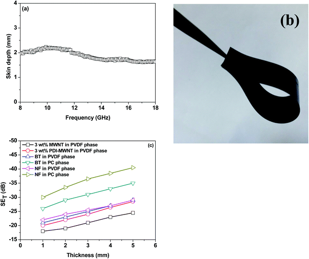 |
| | Fig. 11 Skin depth variation with respect to frequency for the blends with NF in PC phase (a), flexible films derived from blend containing NF-NH2 in the PC phase (b), and thickness variation of the total shielding effectiveness for different blends (c). | |
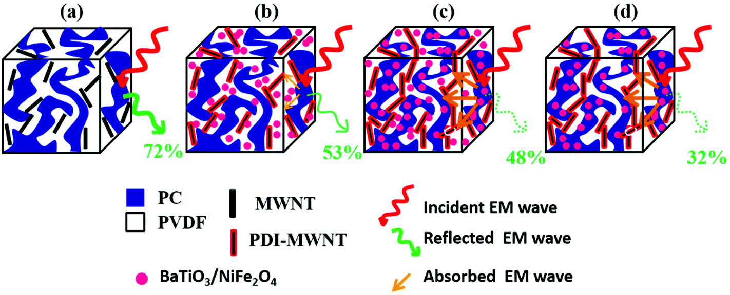
Therefore, the synergetic effects on EM attenuation in the presence of heterogeneous nanoparticles and conducting carbon nanotubes in a co-continuous bi-phasic polymer blend, where we compartmentalized the location of filler particles in two distinct phases, is evident here. For instance, −20 dB of total shielding efficiency indicates that the materials have blocked 99% of EM radiation. Here, we obtained −40 dB of shielding mainly by absorption. This level of EM shielding is recommended for many techno-commercial applications. Thus, this work opens new avenues to invent futuristic EM attenuation shields with very high absorption for a wide range of applications. In Fig. 12 we schematically explain the overall effect of compartmentalized approach in the shielding mechanism.
 |
| | Fig. 12 EM shielding mechanism: (a) shielding is dominated by reflection in the blends with MWNTs in the PVDF phase; (b) shielding is dominated by reflection in the blends where both the nanoparticles (BT/NF, MWNTs) are in the PVDF phase; (c) shielding is primarily by absorption in the blends where the nanoparticles are in both the phases; and (d) shielding is mostly dominated by absorption in the blend where BT/NF nanoparticles are in the PC phase and PDI-MWNT in the PVDF phase. | |
Conclusions
In summary, we have clearly demonstrated that by ordered arrangement of nanoparticles possessing different characteristics (electrical/magnetic dipoles), excellent microwave absorbers can be designed using a co-continuous 50/50 PC/PVDF blends. This is manifested in a high reflection loss of ca. −67 dB for the blend structure where the included conductive materials (MWNT) are in the PVDF phase and NF nanoparticles are in the PC phase of 50/50 co-continuous PC/PVDF blends. The MWNTs were modified using a derivative of perylene diimide that stimulates efficient charge transport in the blends. However, in the case of bi-phasic blends, if the nanoparticles possessing different characteristics are localized in a given phase, the overall shielding efficiency decreases. By adopting a compartmentalized approach, superior EM attenuation can be achieved by absorption. This was realized by comparing the reflection loss for the blend structure where the nanoparticles (MWNTs and BT/NF) were localized exclusively in the PVDF phase or in both the phases against when they were localized in different phases. Interestingly, by adopting the compartmentalized approach where the lossy material (BT or NF) was in the PC phase and the included conductive material (MWNT) was in PVDF, an outstanding reflection loss of ca. −57 dB (for BT and MWNT combination) and −67 dB (for NF and MWNT combination) was achieved and the attenuation occurred primarily through absorption. Hence, this approach demonstrates that nanoscopic structuring in the blends can be achieved under macroscopic processing conditions and this strategy can further be explored to design microwave absorbers.
Acknowledgements
The authors gratefully acknowledge the financial support from DST (India).
References
- Y. Yang, M. C. Gupta, K. L. Dudley and R. W. Lawrence, Nano Lett., 2005, 5, 2131–2134 CrossRef CAS PubMed.
- N. Li, Y. Huang, F. Du, X. He, X. Lin, H. Gao, Y. Ma, F. Li, Y. Chen and P. C. Eklund, Nano Lett., 2006, 6, 1141–1145 CrossRef CAS PubMed.
- H.-B. Zhang, Q. Yan, W.-G. Zheng, Z. He and Z.-Z. Yu, ACS Appl. Mater. Interfaces, 2011, 3, 918–924 CAS.
- J.-M. Thomassin, X. Lou, C. Pagnoulle, A. Saib, L. Bednarz, I. Huynen, R. Jérôme and C. Detrembleur, J. Phys. Chem. C, 2007, 111, 11186–11192 CAS.
- G. P. Kar, S. Biswas, R. Rohini and S. Bose, J. Mater. Chem. A, 2015, 3, 7974–7985 CAS.
- J. Ling, W. Zhai, W. Feng, B. Shen, J. Zhang and W. g. Zheng, ACS Appl. Mater. Interfaces, 2013, 5, 2677–2684 CAS.
- S. Maiti, N. K. Shrivastava, S. Suin and B. B. Khatua, ACS Appl. Mater. Interfaces, 2013, 5, 4712–4724 CAS.
- J. Zhu, S. Wei, N. Haldolaarachchige, D. P. Young and Z. Guo, J. Phys. Chem. C, 2011, 115, 15304–15310 CAS.
- N. Grossiord, J. Loos, O. Regev and C. E. Koning, Chem. Mater., 2006, 18, 1089–1099 CrossRef CAS.
- M. H. Al-Saleh and U. Sundararaj, Carbon, 2009, 47, 1738–1746 CrossRef CAS PubMed.
- H. Pang, L. Xu, D.-X. Yan and Z.-M. Li, Prog. Polym. Sci., 2014, 39, 1908–1933 CrossRef CAS PubMed.
- F. Qin and C. Brosseau, J. Appl. Phys., 2012, 111, 061301 CrossRef PubMed.
- A. Eitan, K. Jiang, D. Dukes, R. Andrews and L. S. Schadler, Chem. Mater., 2003, 15, 3198–3201 CrossRef CAS.
- G. P. Kar, P. Xavier and S. Bose, Phys. Chem. Chem. Phys., 2014, 16, 17811–17821 RSC.
- G. Hu, C. Zhao, S. Zhang, M. Yang and Z. Wang, Polymer, 2006, 47, 480–488 CrossRef CAS PubMed.
- N. G. Sahoo, S. Rana, J. W. Cho, L. Li and S. H. Chan, Prog. Polym. Sci., 2010, 35, 837–867 CrossRef CAS PubMed.
- Y.-L. Zhao and J. F. Stoddart, Acc. Chem. Res., 2009, 42, 1161–1171 CrossRef CAS PubMed.
- D. Baskaran, J. W. Mays and M. S. Bratcher, Chem. Mater., 2005, 17, 3389–3397 CrossRef CAS.
- T. J. Simmons, J. Bult, D. P. Hashim, R. J. Linhardt and P. M. Ajayan, ACS Nano, 2009, 3, 865–870 CrossRef CAS PubMed.
- A. Rasheed, M. D. Dadmun, I. Ivanov, P. F. Britt and D. B. Geohegan, Chem. Mater., 2006, 18, 3513–3522 CrossRef CAS.
- M. N. Tchoul, W. T. Ford, M. L. P. Ha, I. Chavez-Sumarriva, B. P. Grady, G. Lolli, D. E. Resasco and S. Arepalli, Chem. Mater., 2008, 20, 3120–3126 CrossRef CAS.
- R. Rohini and S. Bose, ACS Appl. Mater. Interfaces, 2014, 6, 11302–11310 CAS.
- D. Simien, J. A. Fagan, W. Luo, J. F. Douglas, K. Migler and J. Obrzut, ACS Nano, 2008, 2, 1879–1884 CrossRef CAS PubMed.
- M. Sharma, M. P. Singh, C. Srivastava, G. Madras and S. Bose, ACS Appl. Mater. Interfaces, 2014, 6, 21151–21160 CAS.
- S. P. Pawar, D. A. Marathe, K. Pattabhi and S. Bose, J. Mater. Chem. A, 2015, 3, 656–669 CAS.
- Y. Li and H. Shimizu, Macromolecules, 2008, 41, 5339–5344 CrossRef CAS.
- E. Laredo, M. Grimau, A. Bello, D. F. Wu, Y. S. Zhang and D. P. Lin, Biomacromolecules, 2010, 11, 1339–1347 CrossRef CAS PubMed.
- C. Gao, S. Zhang, F. Wang, B. Wen, C. Han, Y. Ding and M. Yang, ACS Appl. Mater. Interfaces, 2014, 6, 12252–12260 CAS.
- S. Bose, C. Özdilek, J. Leys, J. W. Seo, M. Wübbenhorst, J. Vermant and P. Moldenaers, ACS Appl. Mater. Interfaces, 2010, 2, 800–807 CAS.
- J. Balapanuru, G. Chiu, C. Su, N. Zhou, Z. Hai, Q.-h. Xu and K. P. Loh, ACS Appl. Mater. Interfaces, 2015, 7, 880–886 CAS.
- D. D. L. Chung, Carbon, 2001, 39, 279–285 CrossRef CAS.
- P. Saini, V. Choudhary, N. Vijayan and R. K. Kotnala, J. Phys. Chem. C, 2012, 116, 13403–13412 CAS.
- M. H. Al-Saleh, W. H. Saadeh and U. Sundararaj, Carbon, 2013, 60, 146–156 CrossRef CAS PubMed.
- M.-S. Cao, J. Yang, W.-L. Song, D.-Q. Zhang, B. Wen, H.-B. Jin, Z.-L. Hou and J. Yuan, ACS Appl. Mater. Interfaces, 2012, 4, 6949–6956 CAS.
- M. Rahaman, T. K. Chaki and D. Khastgir, J. Mater. Sci., 2011, 46, 3989–3999 CrossRef CAS.
- S. Nuriel, L. Liu, A. H. Barber and H. D. Wagner, Chem. Phys. Lett., 2005, 404, 263–266 CrossRef CAS PubMed.
|
| This journal is © The Royal Society of Chemistry 2015 |
Click here to see how this site uses Cookies. View our privacy policy here. 
 Open Access Article
 This Open Access Article is licensed under a
  *
*