
 Open Access Article
 This Open Access Article is licensed under a
 Creative Commons Attribution 3.0 Unported Licence
Dimer-on-mirror SERS substrates with attogram sensitivity fabricated by colloidal lithography†
Aron
Hakonen
*a,
Mikael
Svedendahl
a,
Robin
Ogier
a,
Zhong-Jian
Yang
a,
Kristof
Lodewijks
a,
Ruggero
Verre
a,
Timur
Shegai
a,
Per Ola
Andersson
b and
Mikael
Käll
*a
aDepartment of Applied Physics, Division of Bionanophotonics, Chalmers University of Technology, Gothenburg, Sweden. E-mail: hakonen@chalmers.se; kall@chalmers.se
bSwedish Defense Research Agency FOI, Dept CBRN Def & Security, SE-90182 Umea, Sweden
First published on 28th April 2015
Abstract
Nanoplasmonic substrates with optimized field-enhancement properties are a key component in the continued development of surface-enhanced Raman scattering (SERS) molecular analysis but are challenging to produce inexpensively in large scale. We used a facile and cost-effective bottom-up technique, colloidal hole-mask lithography, to produce macroscopic dimer-on-mirror gold nanostructures. The optimized structures exhibit excellent SERS performance, as exemplified by detection of 2.5 and 50 attograms of BPE, a common SERS probe, using Raman microscopy and a simple handheld device, respectively. The corresponding Raman enhancement factor is of the order 1011, which compares favourably to previously reported record performance values.
Surface-enhanced Raman scattering (SERS) has long been considered an extremely promising technique for general and label free identification and trace detection of molecular compounds. The SERS field has gone through several development stages since the original discovery of the effect forty years ago1–4 and the subsequent development of basic understandings of electromagnetic and surface-induced enhancement processes.5–7 After the first single molecule detection reports in the late 90's,8–11 much effort has been devoted to proof-of-principle demonstrations of SERS applications,12–14 studies of the plasmonic origins of the surface-enhancement process15–17 and development of a wide range of SERS substrates, including “SERS dust”18 and nanostructured metal surfaces fabricated by nanosphere lithography (NSL)19 or electron beam lithography (EBL).20
Hole-mask colloidal lithography (HCL)21 is a versatile methodology for fabrication of nanoplasmonic substrates.22,23 An obvious advantage compared to EBL is that macroscopic (>cm2) sample surfaces can be easily prepared. Compared to NSL, the technique is extremely flexible in terms nanostructure geometries: previous examples of nanostructures easily produced by HCL includes, for example, disks, dimers, trimers and cones of various dimensions and shapes.24,25 It is also easy to integrate different materials into the same nanostructure design, for example different metals or combinations of metals and dielectrics.25,26 However, the possibility of using HCL for cost-effective fabrication of SERS substrates has not yet been explored. The primary aim of this study was therefore to find out to what extent HCL substrates can be used for ultra-sensitive SERS measurements. Long-term goals include in-field and non-specialized lab applicability, in particular in the context of terrorist and warfare threats.27–31
We choose to focus on dimer structures because of their well-known and extraordinary electromagnetic field-enhancement in the gap between the particles.32 Details of the fabrication process can be found in the ESI.†Fig. 1a shows a SEM image of HCL gold dimers on glass used for ultra-sensitive SERS analysis. A transect and a 45° tilted view of a substrate fabricated on silicon (to reduce charging effects for better contrast) are shown in Fig. 1b and c, respectively. The dimers consist of slightly conical nanodisks and are all oriented in the same direction as a consequence of the fabrication process, which involves metal evaporation from two opposing angles relative to the surface normal. For the same reason, the two nanodisks composing a dimer have slightly different diameters and height. The gap dimensions vary between different dimers (7.1 ± 4.2 nm std; ndimers = 72; range = 0–18 nm), but there is always gap or crevice of nanometric dimensions between the disks. These locations constitute “hot spots” for SERS. The enhancement caused by localized gap plasmons is further amplified by adding a gold mirror below a thin dielectric (SiO2) spacer layer. The concept of mirror enhancement has recently been demonstrated to be highly useful for amplifying the response of a variety of SERS substrates.33–38 The predominant source of additional enhancement is hybridization between the particle plasmons and propagating plasmon modes in the mirror, although there is also a contribution from classical constructive interference. However, because of the complicated near-field couplings present in the system, the exact spacer distance for optimum enhancement in the plane of the nanostructures critically depends on the nanostructure morphology, materials and wavelength range considered. We focused on fabricating samples suitable for Raman excitation in the red (λ = 638 nm) and a number of finite-difference time domain (FDTD) simulations were done to evaluate optimum system parameters for this particular excitation wavelength. An additional factor to consider is the adhesion at the glass–gold interfaces. The HCL fabrication process includes tape-stripping and therefore requires a rather high adhesion between gold and the adjacent materials, which is usually achieved by including thin adhesion layers of titanium or chromium (Cr). Unfortunately, the adhesion layer strongly dampens the plasmon resonances, thereby dramatically decreasing the enhancement. Simulations were therefore performed for four different systems (exact configurations according Fig. S1a–d in the ESI†), including 2–3 nm chromium layers to assess the Cr influence. Fig. 2a and b illustrate the field enhancement induced through the addition of a gold mirror (without Cr) located 60 nm from the dimers, while Fig. 2c illustrates the almost complete destruction of the enhancement when Cr is present both between the mirror and the SiO2 spacer and underneath the nanoparticles. However, the removal of Cr in direct contact with the dimer leads to an almost full recovery of the hot-spot, as seen in Fig. 2d. Simulations have previously shown that adhesion layers dampen surface plasmons.39 Experimental evidence of this effect for the case of chromium and titanium adhesion layers has also been shown by single molecule fluorescence and SERS studies.40,41 The fact that the mirror adhesion layer has an insignificant dampening is due to its detachment from the dimer hot-spots, which was also found by e.g. Siegfried et al.42
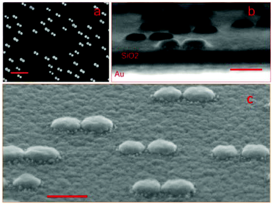 | ||
| Fig. 1 Scanning electron microscopy images of gold nanodimers. (a) Top-view of dimers on SiO2 spacer on gold mirror fabricated on top of a glass cover-slide. Scalebar = 500 nm. (b) Transect in near vertical view (tilted 10°) of the mirror, spacer and dimers. Scalebar = 100 nm. (c) 45° view of the dimers. Scalebar = 100 nm. | ||
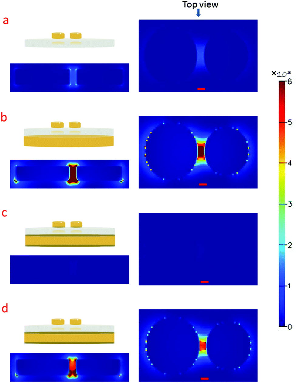 | ||
| Fig. 2 The dimer-spacer-mirror configurations (top left in each panel) and the corresponding intensity enhancement (|E/E0|2) in side-view (lower left) and top-view (right) for an incident plane wave with wavelength 681 nm and polarization along the dimer axis. Panel (a) and (b) compares the case with and without a gold mirror 60 nm below the SiO2. Case (c) shows the case when 2 nm Cr adhesion layers are present on all metal–dielectric interfaces while (d) shows the case when Cr is present on the mirror but not between the dimer and the SiO2. The red scalebars are 10 nm long, which is the same as the gap size. | ||
The variation in Raman enhancement, estimated as the fourth power of the local field-enhancement factor, with SiO2 spacer thickness was assessed for the case of a 100 nm thick gold mirror with Cr adhesion layers on both sides but no Cr under the dimers (geometry as Fig. 2d and S1d†). Fig. 3 shows that the highest Raman enhancement is obtained for the 60 nm spacer thickness and that the amplification compared to the peak enhancement of the mirror-free structure is of the order ∼200. Interestingly, the simulated reflectance spectrum for the structure with the optimized spacer thickness shows near complete absorption of the incident light (Fig. S2†). Angular dependent perfect absorption has previously been shown for HCL fabricated surfaces, where the underlying physics explaining the phenomenon was a destructive Fano interference.43,44 The experimental reflectance of a dimer/mirror sample with a 60 nm spacer (Fig. S3†) shows considerable inhomogeneous broadening but a resonance position close to the simulation result.
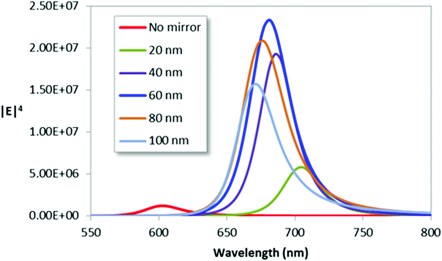 | ||
| Fig. 3 Simulated Raman enhancement (∼|E/E0|4) versus wavelength for dimers on a SiO2 spacer of varying thickness above a Cr coated gold mirror compared to the case when no mirror is present. The enhancement is evaluated in the middle of the gap 10 nm above the substrate surface. | ||
Key results from micro-Raman measurements on trans-1,2-bis(4-pyridyl)ethylene (BPE), a common test molecule for evaluating the performance of SERS substrates,45–49 are summarized in Fig. 4. The test solution was applied to the substrate by drop-casting and left to dry. Initial spreading is a few mm2, however, most molecules are concentrated into the final evaporation imprint, which has an estimated maximum diameter of 200 μm. Note that BPE has much higher affinity towards the gold than to SiO2, so it is unlikely that a significant fraction of the molecules bind to the dielectric interface.
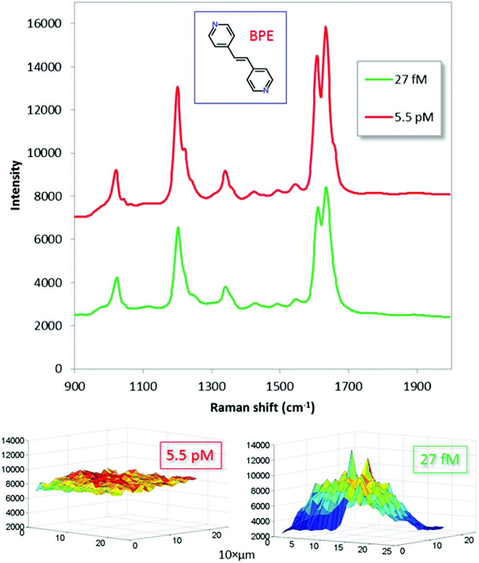 | ||
| Fig. 4 SERS spectra averaged over a 200 × 200 μm area (441 points) of gold dimers incubated with low concentration solutions of drop-casted (0.5 μl) and evaporated BPE (inset). The excitation wavelength was 638 nm. The solution concentrations were: 2.7 × 10⁻¹⁴ M (red, shifted vertically for clarity) and 5.5 × 10⁻¹² M (green). Corresponding Raman intensity maps for the 1640 cm−1 peak are shown in the bottom row. The Raman microscope was equipped with a 10×/NA = 0.2 objective, which produced a ∼10 μm diameter laser spot size. The laser power was ∼2 mW and the integration time was 1 s per point. | ||
The optimized substrates displayed strong Raman signals for all five major BPE peaks down to 2.7 × 10⁻¹⁴ M, which corresponds to 2.5 attogram loaded on the substrate (0.5 μl droplet). Experiments indicated that even lower concentrations could be measured, though the signal-to-background was poor. This suggests that it is possible to attain single molecule sensitivity using our dimer-on-mirror substrates. Note, however, that the Raman signal is highly non-linearly dependent on load: there are ∼200 times more molecules present per area unit for the higher concentration (5.5 pM) than for the low one (27 fM), yet the average SERS signal is only ∼50% stronger. This clearly indicates a saturation effect due to a limited number of “hot gap sites”50 and perhaps also an active process due to the drying step that attracts the analyte molecules specifically to these sites. It is thus possible the sensitivity in terms of δI/δC follows a hot-spot depletion dependent power law, as has previously been shown by for example Fang et al.50 and Le Ru et al.51 Assuming that the majority of the molecules are concentrated into the measured area, the lowest concentration in Fig. 4 would correspond to approximately 20 molecules per measurement spot.
Normal Raman measurements on a water solution containing BPE at a concentration (4 mM) close to the theoretical dissolution limit61 gave no signals for integration times up to about a minute. Estimates of average surface-enhancement factors (EF) were therefore based on comparisons with Raman measurements on a single BPE crystal smaller than the experimentally determined excitation spot-size (d = 6 μm for the crystal, vs. 10 μm). Scans around the single crystal were done to find the highest spot-on intensity (692 counts). The number of molecules contributing to the Raman signal NRaman was estimated from the crystal volume (∼1.1 × 10⁻¹⁶ m3) and density (1100 kg m−3), while NSERS was estimated from the total load of BPE molecules divided by the number of scanned spots. The EFs were then calculated as:62 EF = (ISERS/NSERS)/(IRaman/NRaman). We used the 27 fM concentration for an estimate of the ensemble EF. With 20 molecules per measurement spot (assuming that all molecules contribute to the signal) results in an average EF of ∼2.1 × 10¹¹ for the 1633 cm−1 peak. This extremely high EF value is of the same order, ∼1011, as the approximate limit for the electromagnetic enhancement for “gapped” gold and silver nanostructures excited with visible light.20 As shown by the simulations (Fig. 3), the Raman enhancement at the hottest locations of the dimer-on-mirror substrates reaches only ∼107. Thus the discrepancy between the calculations and the experiment is about 4–5 orders of magnitude. However, the actual experimental system contains a significant fraction of dimers with much smaller gaps and it is likely that these contribute disproportionally much to the measured signal. It is also highly likely that an multiplicative chemisorption induced resonance Raman effect contribute to the total surface-enhancement for the case of BPE, and that the actual electromagnetically induced enhancement effect therefore is one or up to three orders of magnitude lower then this estimate.63,64 Indeed, extensive quantum chemistry calculations of BPE chemisorbed to Au-clusters have indicated a substantial molecule-to-metal charge transfer45 that could form the basis for a “chemical” enhancement process along the lines described in e.g. Persson.65 Note also that the simulations do not take into account surface roughness, which might also contribute additional electromagnetic enhancement. The enhancement factor obtained here compares favourably to some of the highest ensemble EF values previously reported in the literature (Table 1). However, one should be aware that the methodology used to experimentally estimate EF values vary considerably between researchers and is sometimes inadequately described. The comparison in Table 1 should therefore only serve as an indicator of SERS substrate performance.
| Reference | Molecule | EF |
|---|---|---|
| Ahn et al.52 | Crystal violet | >109 |
| Li et al.53 | BPE | 1.2 × 10⁹ |
| Chakraborty et al.54 | Crystal violet | 1.6 × 10⁹ |
| Zhang et al.55 | R6G | 1010 |
| Yang et al.56 | R6G | 1.2 × 10¹⁰ |
| Seo et al.57 | Methylene blue | 3.0 × 10¹⁰ |
| Leem et al.58 | Glucose | 4.2 × 10¹⁰ |
| Lee et al.59 | R6G | 1011 |
| Present study | BPE | 1.2 × 10¹¹ |
| Chirumamilla et al.60 | p-Mercaptoaniline | 3.5 × 10¹¹ |
| Ko et al.29 | 2,4-DNT | >1012 |
To demonstrate potential for in-field applicability, low-level detection with a commercial portable Raman instrument was assessed. The instrument (Thermo Scientific® FirstDefender RM™) is compact and lightweight (800 grams), operates using a 785 nm diode laser, contain simple non-moving optics and an un-cooled CCD detector. Fig. 5 shows SERS data for 5.5 × 10⁻¹³ and 5.5 × 10⁻¹¹ M BPE together with a blank control. The results indicate high-performance in-field and non-specialized lab capabilities. The lowest detected concentration corresponds to a total of 270 zeptomol (50 attogram) loaded on the substrate (0.5 μl). For the 1020 cm−1 peak a signal-to-noise ratio of 12 could be calculated, indicating even lower detection capabilities. The higher limit-of-detection obtained for the portable device relative to the micro-Raman results is likely caused by differences in excitation and collection efficiency, excitation wavelength, background contributions and difficulties in pin-pointing the final evaporated droplet without the help of a microscope.
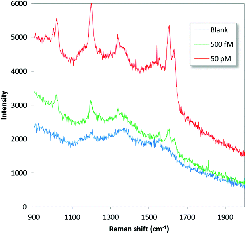 | ||
| Fig. 5 Rawdata for 0.5 μL evaporated droplets with 0 (blue), 5 × 10⁻¹¹ (green) and 5 × 10⁻¹³ (red) M BPE acquired with the handheld Raman instrument. The excitation wavelength was 785 nm (max 240 mW) and the integration time 10 s. | ||
At present the substrates cannot be used for reversible sensing of molecules with high affinity to gold such as BPE. However, the substrates are quite large (500 mm2), while the analyzed droplets are small (here 0.5 μl). Hence, >30 such droplets can be placed on a single substrate, which means that both calibration solutions and several samples can be measured on the same substrate.
Conclusions
We evaluated the SERS performance of gold dimer-on-mirror nanostructures made by colloidal hole-mask lithography. Electrodynamics simulations indicated an optimum mirror – dimer separation of 60 nm and revealed that Cr adhesion layers can have serious negative impact on the enhancement performance. The optimized structure configuration was used to detect ultra-low quantities of BPE, a common SERS probe molecule. Mass detection of 2.5 and 50 attogram of BPE was demonstrated with a Raman microscope and a handheld device, respectively. The former value translate to SERS enhancement factor of the order ∼1011, similar to some of the highest enhancement results found in the literature. The colloidal lithography method is extremely versatile and it is likely that a wide range of other structure types with excellent SERS performance can be constructed based on a similar methodology as employed here. One of the most important goals for such developments should be to improve the dynamic range of SERS sensor substrate by increasing the number of “hot spots” per area unit.Acknowledgements
This work was funded by The Swedish Foundation for Strategic Research (project RMA11-0037). TS and POA acknowledges additional financial support the Swedish Research Council and the Swedish Defence Materiel Administration, FMV (Project no. E4884 and E4878 at FOI), respectively.Notes and references
- M. Fleischmann, P. J. Hendra and A. J. McQuillan, Chem. Phys. Lett., 1974, 26, 163–166 CrossRef CAS.
- Y. J. Chen, W. P. Chen and E. Burstein, Phys. Rev. Lett., 1976, 36, 1207–1210 CrossRef CAS.
- D. L. Jeanmaire and R. P. Vanduyne, J. Electroanal. Chem., 1977, 84, 1–20 CrossRef CAS.
- M. Moskovits, J. Chem. Phys., 1978, 69, 4159–4161 CrossRef CAS PubMed.
- M. Moskovits, Rev. Mod. Phys., 1985, 57, 783–826 CrossRef CAS.
- A. Otto, I. Mrozek, H. Grabhorn and W. Akemann, J. Phys.: Condens. Matter, 1992, 4, 1143–1212 CrossRef CAS.
- A. Campion and P. Kambhampati, Chem. Soc. Rev., 1998, 27, 241–250 RSC.
- S. Nie and S. R. Emory, Science, 1997, 275, 1102–1106 CrossRef CAS PubMed.
- K. Kneipp, Y. Wang, H. Kneipp, L. T. Perelman, I. Itzkan, R. Dasari and M. S. Feld, Phys. Rev. Lett., 1997, 78, 1667–1670 CrossRef CAS.
- H. X. Xu, E. J. Bjerneld, M. Käll and L. Börjesson, Phys. Rev. Lett., 1999, 83, 4357–4360 CrossRef CAS.
- A. M. Michaels, M. Nirmal and L. E. Brus, J. Am. Chem. Soc., 1999, 121, 9932–9939 CrossRef CAS.
- X. M. Qian, X. H. Peng, D. O. Ansari, Q. Yin-Goen, G. Z. Chen, D. M. Shin, L. Yang, A. N. Young, M. D. Wang and S. M. Nie, Nat. Biotechnol., 2008, 26, 83–90 CrossRef CAS PubMed.
- K. Hering, D. Cialla, K. Ackermann, T. Dorfer, R. Moller, H. Schneidewind, R. Mattheis, W. Fritzsche, P. Rosch and J. Popp, Anal. Bioanal. Chem., 2008, 390, 113–124 CrossRef CAS PubMed.
- R. A. Alvarez-Puebla and L. M. Liz-Marzan, Small, 2010, 6, 604–610 CrossRef CAS PubMed.
- H. X. Xu, X. H. Wang, M. P. Persson, H. Q. Xu, M. Käll and P. Johansson, Phys. Rev. Lett., 2004, 93, 4 Search PubMed.
- E. C. LeRu and P. G. Etchegoin, Principles of Surface-Enhanced Raman Spectroscopy: And Related Plasmonic Effects, Elsevier Science Bv, Amsterdam, 2009 Search PubMed.
- J. R. Lombardi and R. L. Birke, J. Phys. Chem. C, 2008, 112, 5605–5617 CAS.
- J. F. Li, Y. F. Huang, Y. Ding, Z. L. Yang, S. B. Li, X. S. Zhou, F. R. Fan, W. Zhang, Z. Y. Zhou, D. Y. Wu, B. Ren, Z. L. Wang and Z. Q. Tian, Nature, 2010, 464, 392–395 CrossRef CAS PubMed.
- C. L. Haynes and R. P. Van Duyne, J. Phys. Chem. B, 2001, 105, 5599–5611 CrossRef CAS.
- L. Gunnarsson, E. J. Bjerneld, H. Xu, S. Petronis, B. Kasemo and M. Käll, Appl. Phys. Lett., 2001, 78, 802–804 CrossRef CAS PubMed.
- H. Fredriksson, Y. Alaverdyan, A. Dmitriev, C. Langhammer, D. S. Sutherland, M. Zäch and B. Kasemo, Adv. Mater., 2007, 19, 4297–4302 CrossRef CAS PubMed.
- J. H. Zhang, Y. F. Li, X. M. Zhang and B. Yang, Adv. Mater., 2010, 22, 4249–4269 CrossRef CAS PubMed.
- M. R. Jones, K. D. Osberg, R. J. Macfarlane, M. R. Langille and C. A. Mirkin, Chem. Rev., 2011, 111, 3736–3827 CrossRef CAS PubMed.
- T. Shegai, P. Johansson, C. Langhammer and M. Käll, Nano Lett., 2012, 12, 2464–2469 CrossRef CAS PubMed.
- T. Shegai, S. Chen, V. D. Miljkovic, G. Zengin, P. Johansson and M. Käll, Nat. Commun., 2011, 2, 481 CrossRef PubMed.
- A. Dmitriev, C. Hägglund, S. Chen, H. Fredriksson, T. Pakizeh, M. Käll and D. S. Sutherland, Nano Lett., 2008, 8, 3893–3898 CrossRef CAS PubMed.
- X. Y. Zhang, M. A. Young, O. Lyandres and R. P. Van Duyne, J. Am. Chem. Soc., 2005, 127, 4484–4489 CrossRef CAS PubMed.
- S. S. R. Dasary, A. K. Singh, D. Senapati, H. T. Yu and P. C. Ray, J. Am. Chem. Soc., 2009, 131, 13806–13812 CrossRef CAS PubMed.
- H. Ko, S. Chang and V. V. Tsukruk, ACS Nano, 2009, 3, 181–188 CrossRef CAS PubMed.
- J. M. Sylvia, J. A. Janni, J. D. Klein and K. M. Spencer, Anal. Chem., 2000, 72, 5834–5840 CrossRef CAS.
- A. Hakonen, P. O. Andersson, M. Stenbæk Schmidt, T. Rindzevicius and M. Käll, Anal. Chim. Acta, 2015 DOI:10.1016/j.aca.2015.04.010.
- J. P. Camden, J. A. Dieringer, Y. M. Wang, D. J. Masiello, L. D. Marks, G. C. Schatz and R. P. Van Duyne, J. Am. Chem. Soc., 2008, 130, 12616–12617 CrossRef CAS PubMed.
- J. Ye, M. Shioi, K. Lodewijks, L. Lagae, T. Kawamura and P. Van Dorpe, Appl. Phys. Lett., 2010, 97, 3 Search PubMed.
- S. Mubeen, S. Zhang, N. Kim, S. Lee, S. Krämer, H. Xu and M. Moskovits, Nano Lett., 2012, 12, 2088–2094 CrossRef CAS PubMed.
- A. Chen, R. L. Miller, A. E. DePrince, A. Joshi-Imre, E. Shevchenko, L. E. Ocola, S. K. Gray, U. Welp and V. K. Vlasko-Vlasov, Small, 2013, 9, 1939–1946 CrossRef CAS PubMed.
- D. X. Wang, W. Q. Zhu, M. D. Best, J. P. Camden and K. B. Crozier, Sci. Rep., 2013, 3, 6 Search PubMed.
- J. Lee, B. Hua, S. Park, M. Ha, Y. Lee, Z. Fan and H. Ko, Nanoscale, 2014, 6, 616–623 RSC.
- C.-C. Yu, Y.-C. Tseng, P.-Y. Su, K.-T. Lin, C.-C. Shao, S.-Y. Chou, Y.-T. Yen and H.-L. Chen, Nanoscale, 2015, 7, 3985–3996 RSC.
- X. J. Jiao, J. Goeckeritz, S. Blair and M. Oldham, Plasmonics, 2009, 4, 37–50 CrossRef CAS.
- H. Aouani, J. Wenger, D. Gérard, H. Rigneault, E. Devaux, T. W. Ebbesen, F. Mahdavi, T. Xu and S. Blair, ACS Nano, 2009, 3, 2043–2048 CrossRef CAS PubMed.
- T. G. Habteyes, S. Dhuey, E. Wood, D. Gargas, S. Cabrini, P. J. Schuck, A. P. Alivisatos and S. R. Leone, ACS Nano, 2012, 6, 5702–5709 CrossRef CAS PubMed.
- T. Siegfried, Y. Ekinci, O. J. F. Martin and H. Sigg, ACS Nano, 2013, 7, 2751–2757 CrossRef CAS PubMed.
- M. Svedendahl, P. Johansson and M. Käll, Nano Lett., 2013, 13, 3053–3058 CrossRef CAS PubMed.
- M. Svedendahl and M. Käll, ACS Nano, 2012, 6, 7533–7539 CrossRef CAS PubMed.
- A. Mohammed, W. Hu, P. O. Andersson, M. Lundquist, L. Landström, Y. Luo and H. Ågren, Chem. Phys. Lett., 2013, 581, 70–73 CrossRef CAS PubMed.
- J. P. Singh, H. Y. Chu, J. Abell, R. A. Tripp and Y. P. Zhao, Nanoscale, 2012, 4, 3410–3414 RSC.
- A. T. Zayak, H. Choo, Y. S. Hu, D. J. Gargas, S. Cabrini, J. Bokor, P. J. Schuck and J. B. Neaton, J. Phys. Chem. Lett., 2012, 3, 1357–1362 CrossRef CAS.
- W. H. Yang, J. Hulteen, G. C. Schatz and R. P. VanDuyne, J. Chem. Phys., 1996, 104, 4313–4323 CrossRef CAS PubMed.
- K. Wu, T. Rindzevicius, M. S. Schmidt, K. B. Mogensen, A. Hakonen and A. Boisen, J. Phys. Chem. C, 2015, 119, 2053–2062 CAS.
- Y. Fang, N. H. Seong and D. D. Dlott, Science, 2008, 321, 388–392 CrossRef CAS PubMed.
- E. C. Le Ru, P. G. Etchegoin and M. Meyer, J. Chem. Phys., 2006, 125, 13 CrossRef PubMed.
- H. J. Ahn, P. Thiyagarajan, L. Jia, S. I. Kim, J. C. Yoon, E. L. Thomas and J. H. Jang, Nanoscale, 2013, 5, 1836–1842 RSC.
- W. D. Li, F. Ding, J. Hu and S. Y. Chou, Opt. Express, 2011, 19, 3925–3936 CrossRef PubMed.
- I. Chakraborty, S. Bag, U. Landman and T. Pradeep, J. Phys. Chem. Lett., 2013, 4, 2769–2773 CrossRef CAS.
- J. Zhang, X. Zhang, C. Lai, H. Zhou and Y. Zhu, Opt. Express, 2014, 22, 21157–21166 CrossRef PubMed.
- Y. Yang, Z. Y. Li, K. Yamaguchi, M. Tanemura, Z. R. Huang, D. L. Jiang, Y. H. Chen, F. Zhou and M. Nogami, Nanoscale, 2012, 4, 2663–2669 RSC.
- S. H. Seo, B. M. Kim, A. Joe, H. W. Han, X. Y. Chen, Z. Cheng and E. S. Jang, Biomaterials, 2014, 35, 3309–3318 CrossRef CAS PubMed.
- J. Leem, H. W. Kang, S. H. Ko and H. J. Sung, Nanoscale, 2014, 6, 2895–2901 RSC.
- H. K. Lee, Y. H. Lee, Q. Zhang, I. Y. Phang, J. M. R. Tan, Y. Cui and X. Y. Ling, ACS Appl. Mater. Interfaces, 2013, 5, 11409–11418 CAS.
- M. Chirumamilla, A. Toma, A. Gopalakrishnan, G. Das, R. P. Zaccaria, R. Krahne, E. Rondanina, M. Leoncini, C. Liberale, F. De Angelis and E. Di Fabrizio, Adv. Mater., 2014, 26, 2353–2358 CrossRef CAS PubMed.
- E. P. I. Suite™, United States Environmental Protection Agency, Washington, DC, USA, 2012 Search PubMed.
- E. C. Le Ru, E. Blackie, M. Meyer and P. G. Etchegoin, J. Phys. Chem. C, 2007, 111, 13794–13803 CAS.
- H. X. Xu, J. Aizpurua, M. Käll and P. Apell, Phys. Rev. E: Stat. Phys., Plasmas, Fluids, Relat. Interdiscip. Top., 2000, 62, 4318–4324 CrossRef CAS.
- T. Shegai, A. Vaskevich, I. Rubinstein and G. Haran, J. Am. Chem. Soc., 2009, 131, 14390–14398 CrossRef CAS PubMed.
- B. Persson, Chem. Phys. Lett., 1981, 82, 561–565 CrossRef CAS.
Footnote |
| † Electronic supplementary information (ESI) available. See DOI: 10.1039/c5nr01654a |
| This journal is © The Royal Society of Chemistry 2015 |