
 Open Access Article
 This Open Access Article is licensed under a
 Creative Commons Attribution 3.0 Unported Licence
Collective excitation of plasmonic hot-spots for enhanced hot charge carrier transfer in metal/semiconductor contacts†
Adrien
Piot
ab,
Stuart K.
Earl
c,
Charlene
Ng
bd,
Svetlana
Dligatch
e,
Ann
Roberts
c,
Timothy J.
Davis
bd and
Daniel E.
Gómez
*bd
aInstitut National des Sciences Appliquées de Toulouse, 135 Avenue de Rangueil, 31400, Toulouse, France
bMelbourne Centre for Nanofabrication, Australian National Fabrication Facility, Clayton, VIC 3168, Australia
cSchool of Physics, The University of Melbourne, Parkville, VIC 3010, Australia
dCSIRO, Manufacturing Flagship, Private Bag 33, Clayton, VIC 3168, Australia. E-mail: daniel.gomez@csiro.au
eCSIRO, Manufacturing Flagship, PO Box 218, Lindfield, NSW 2070, Australia
First published on 9th April 2015
Abstract
We show how a combination of near- and far-field coupling of the localised surface plasmon resonances in aluminium nanoparticles deposited on TiO2 films greatly enhances the visible light photocatalytic activity of the semiconductor material. We demonstrate two orders of magnitude enhancement in the rate of decomposition of methylene blue under visible light illumination when the surface of TiO2 films is decorated with gratings of Al nanoparticle dimers.
Photocatalysis with semiconductor materials has great potential for the direct conversion of solar to chemical energy. A photocatalyst material after absorbing light energy, creates highly energetic charge carriers that can drive useful chemical transformations, including production of fuels by solar energy (e.g. hydrogen from water splitting1–5 and hydrocarbons from CO2 (ref. 6)), the production of high-value fine chemicals (e.g. ethylene oxide7) and the elimination of hazardous contaminants from air and water (e.g. nitrous oxides, etc.). Conventional photocatalytic processes are however not very efficient.8 Suitable semiconductor materials for photocatalysis (i) only absorb light in the UV region of the solar spectrum (less than 10% of the total available solar energy) (ii) exhibit fast recombination of the photo-excited charge carriers which additionally (iii) have small diffusion lengths, factors which add up to low photocatalytic efficiencies.
Plasmonic enhanced photocatalysis9–14 has resurfaced as a very effective approach for increasing the efficiency of photocatalytic processes. In this approach, nanoparticles of coinage metals (predominantly Ag and Au) are placed either in direct contact or in the vicinity of the photocatalytic material, leading to increased generation of chemically useful electron–hole pairs as a result of several surface plasmon related mechanisms that mitigate some of the intrinsic shortcomings listed above.
One such mechanism involves the transfer of hot-electrons from metal nanoparticles into the photocatalytic material, in an analogous manner to dye sensitization in solar cells.15–17 Absorption of light by metal nanoparticles, through photoexcitation of localised surface plasmon resonances (LSPRs), can result (after non-radiative relaxation) in the formation of hot-electrons: a transient population of electrons with energies between the vacuum and the Fermi level of the metal.14 When the metal is in direct contact with the semiconductor material, a Schottky energy barrier ϕSB occurs (see Fig. 1) and the efficiency of hot-electron transfer is proportional to the fraction of the hot-electron population which has enough energy to overcome this barrier.18 Given that in general ϕSB is much smaller than the band-gap of the semiconducting material, the generation of chemically useful16 charge carriers via this mechanism extends the response of the combined photocatalytic system to the visible and near-infrared regions of the spectrum.19
 | ||
| Fig. 1 Aluminium gap nanoantennas are deposited on top of 190 nm films of TiO2. The antennas are periodically arranged on the substrate. The periodicity of the array is optimised to achieve a collective in-phase dipolar coupling on the nanoantennas. The diagram on the right illustrates the idealised energy band alignment at the metal/semiconductor interface. Non-radiative plasmon relaxation produces a hot-electron that is transferred above the Schottky barrier ϕSB to TiO2. The charge separated state initiates charge transfer processes in solution. | ||
According to White and Catchpole,18 the metal-to-semiconductor hot-electron photo-current jsc can be estimated with the following equation:
| jsc = e∫S(λ)σabs(λ)η(λ,ϕSB)dλ | (1) |
The Schottky barrier between Au and TiO2 is in the order of 0.9 to 1.0 eV![[thin space (1/6-em)]](https://www.rsc.org/images/entities/char_2009.gif) 20 which implies that the fraction of hot-electrons with sufficient energy to cross the barrier η(λ,ϕSB) is about 20% to 40%21 at the wavelengths of the LSPRs18 (see the ESI†). In spite of this limitation, several reports exist where Au nanoparticles have greatly enhanced the photocatalytic activity (and photocurrents) of TiO2.22 The fraction η(λ,ϕSB) of hot-electrons could be increased to >70% by using aluminium, an abundant and relatively inexpensive metal that has a more positive work function and consequently a smaller associated metal-semiconductor Schottky barrier (see detailed estimate in the ESI†).
20 which implies that the fraction of hot-electrons with sufficient energy to cross the barrier η(λ,ϕSB) is about 20% to 40%21 at the wavelengths of the LSPRs18 (see the ESI†). In spite of this limitation, several reports exist where Au nanoparticles have greatly enhanced the photocatalytic activity (and photocurrents) of TiO2.22 The fraction η(λ,ϕSB) of hot-electrons could be increased to >70% by using aluminium, an abundant and relatively inexpensive metal that has a more positive work function and consequently a smaller associated metal-semiconductor Schottky barrier (see detailed estimate in the ESI†).
According to eqn (1), the second parameter that affects the hot-electron photocurrent is σabs(λ), the optical absorption cross section of the metal nanoparticles which can be controlled by the shape and geometrical arrangement of the metal particles. Al nanoparticles typically exhibit localised surface plasmon resonances in the UV region23–26 but when placed in direct contact with high refractive index materials, such as TiO2, these LSPRs can be shifted to the visible light.27
In this communication, we have demonstrated how diffractive coupling in Al nanoparticles leads to significant enhancements in the photocatalytic activity of TiO2 using visible light. Our approach exploits plasmonic coupling effects at two length scales to maximise visible light absorption by the plasmonic array. The concept is illustrated in Fig. 1. The unit cell of the plasmonic arrays consists of Al nanorod dimers with tip-to-tip separation distances of about 20 nm. At these deep sub-wavelength distances, near-field interactions lead to plasmonic hybridization28 resulting in local electromagnetic field densities that can be many orders of magnitude higher than the incident field (i.e. plasmonic hot-spots),29 an effect that has recently been employed for achieving one order of magnitude enhancement in surface enhanced infra-red spectroscopy.30 These Al dimers are periodically arranged on the surface of the thin (190 nm) films of TiO2 with a period that results in a collective excitation of all the dimers in the array and consequently in the absorption of light that far exceeds that of the non-interacting Al dimers.31
Light absorbed by these strongly coupled arrays results, after surface plasmon non-radiative relaxation, in hot charge carrier transfer from the Al dimers to the semiconductor substrate, an efficient process for Al/TiO2 in the visible region of the spectrum.‡ This charge transfer initiates redox reactions at the metal and semiconductor interfaces.
We arbitrarily choose the geometry of the unit cell of the arrays of Fig. 1 for it to exhibit particle plasmon resonances in the visible region of the spectrum. With a fixed geometry for the unit cell, the next step in the design consists of optimising the value of the periodicity of the lattice required to achieve in-phase diffractive dipole–dipole interactions:32–37 for a single Al dimer, the driving electromagnetic field is simply given by the incident field  . For a periodic array, the local field
  that excites each nanoparticle is a superposition of the incident field and the field created by the other nanoparticles in the array:
 | (2) |
In Fig. 2(A) we show how the calculated absorption spectra change with the periodicity of the array where in addition to spectral red-shifts with increasing period, changes in the magnitude of the absorption are also evident. The dominant absorption band reaches a maximum for an array period of 300 nm; this enhanced absorption originates from the in-phase collective oscillation of the LSPRs of the Al dimers. These bands occur at wavelengths λ where the diffractive order (i, j) of the periodic array transitions from evanescent to radiative,31 a condition approximately given by:36
 | (3) |
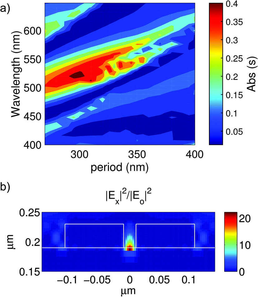 | ||
| Fig. 2 (A) Calculated absorption spectra of Al dimer arrays for different periods for s polarization. The width of each nanorod was 80 nm, length 100 nm, height 40 nm and the face-to-face distance was fixed at 20 nm. The metal particles were assumed to be deposited on top of 190 nm TiO2 thin films. (B) Calculated spatial distribution of the x-component of the electric field at the 520 nm resonance. It is clear that a plasmonic hot-spot occurs at the gap of the nanorods and furthermore most of this electric field is confined to the TiO2 space. | ||
To realise these systems that exhibit collective excitation of plasmonic hot-spots, we fabricated arrays of Al nanorod dimers using top-down electron beam lithography on glass slides coated with 190 nm TiO2 thin films.§ This top-down nanofabrication approach results in naked surfaces (i.e. free of ligands) which favour interfacial charge transfer. A scanning electron microscopy image of one such array is shown in Fig. 3(A). In Fig. 3(B) we show the spectrum of the extinction of the array (shown as 1 − transmittance¶). The spectrum exhibits many spectral features but the dominant one occurs around 520 nm in close agreement with the estimate given by eqn (2) and the numerical simulations of Fig. 2.
 | ||
| Fig. 3 (A) A scanning electron microscopy (SEM) image of a square array of Al nanodimers with a period of 300 nm, shown at two different size scales. (B) Extinction spectra (1 − T) of the fabricated arrays measured with unpolarised light. (C) Change in absorbance of a 50 ppm solution of methylene blue contained inside a microfluidic channel on top of a 3 × 3 mm2 array of Al nanoantenna dimers with 540 nm illumination (bandwidth of 40 nm). | ||
The spectral band at 520 nm is very narrow and intense, which is characteristic of the excitation of a collective mode with suppressed radiative damping.35 The spectrum also has regions of very suppressed absorptions (at ∼490 nm and ∼600 nm) which could be accounted for by considering the destructive interference between the waveguided modes at the TiO2 films and the particle plasmon resonances.33,38 At this 520 nm wavelength, light normally incident on the array excites a collective plasmonic oscillation which concentrates most of the electromagnetic energy on the hot spots located at the nanodimer gap [see Fig. 2(B)]. Non-radiative relaxation of this collective oscillation could result in the excitation of hot electrons on the Al nanodimers which could be transferred into the underlying TiO2 film.
As a test of this hypothesis, we measured the rate of degradation of methylene blue (MB) by following spectroscopically a decrease in the absorption band of MB at 665 nm upon illumination with spectrally filtered light from a Hg lamp (centred at 550 nm with a 40 nm band pass). MB decomposition by TiO2 is a convenient test reaction because it can be followed spectroscopically in the visible region of the spectrum and it is also a well understood reaction that is initiated by charge transfer processes as depicted in Fig. 1:39 the Al nanoparticles inject holes into MB molecules and the TiO2 film injects electrons into dissolved oxygen. The resulting charged species undergo a number of transformations that eventually lead to a net decomposition of MB into smaller molecules.39
The measured absorbance decay (ΔA) (Fig. 3(C)) is directly proportional to the change in concentration of MB. For the bare TiO2 substrate, the observed ΔA time decay was accurately described by a first-order kinetic decay (single exponential) yielding a rate constant of k = 5.6 × 10⁻⁶ s−1. In contrast, for the Al nanodimer array we found that the decay was bi-exponential with rates k1 = 1.13 × 10⁻¹ s−1 and k2 = 1.28 × 10⁻⁵ s−1, which are ∼104 and ∼2 times higher than the one obtained for the bare TiO2 substrate. An average decay rate 〈k〉 = 8.18 × 10⁻⁴ s−1 can be estimated from the bi-exponential fit|| which is about 150 times larger than the one observed for the bare TiO2 substrate (which exhibits a low rate due to its poor absorption of visible light). This result would seem to confirm our hypothesis and furthermore, it seems to imply that hole transfer from Al nanoparticles to MB molecules in solution [see Fig. 1] occurs in spite of the documented evidence that Al nanoparticles self-terminate with a 3–5 nm oxide layer when exposed to ambient air.26
We have demonstrated how the periodic arrangement of metal nanoparticles on a photocatalytic substrate leads to strong collective plasmon resonances. These strong optical responses are translated into augmented rates of hot-electron generation and consequent enhanced redox reaction rates. Our proof-of-concept demonstration is not just limited to variations in the periodicity of deposited nanostructures; in contrast, lithographic nanofabrication enables unparalleled control over the geometry of the nanoparticles, which we anticipate to have as yet to be explored effects on the enhancement of photochemical processes.
This work was performed in part at the Melbourne Centre for Nanofabrication (MCN) in the Victorian Node of the Australian National Fabrication Facility (ANFF). A. P. was jointly supported by the MCN and CSIRO. C. N. was supported by an OCE Fellowship from CSIRO. D. E. G. acknowledges the ARC for support through a Future Fellowship (FT140100514) and F. Eftekhari for fruitful advise on EBL and L. Hyde for his help on ellipsometric measurements. D. E. G. and T. J. D. acknowledge the ANFF for the MCN Technology Fellowships.
References
- H. M. Chen, C. K. Chen, C.-J. Chen, L.-C. Cheng, P. C. Wu, B. H. Cheng, Y. Z. Ho, M. L. Tseng, Y.-Y. Hsu, T.-S. Chan, J.-F. Lee, R.-S. Liu and D. P. Tsai, ACS Nano, 2012, 6, 7362–7372 CrossRef CAS PubMed.
- J. Lee, S. Mubeen, X. Ji, G. D. Stucky and M. Moskovits, Nano Lett., 2012, 12, 5014–5019 CrossRef CAS PubMed.
- D. B. Ingram and S. Linic, J. Am. Chem. Soc., 2011, 133, 5202–5205 CrossRef CAS PubMed.
- Z. Liu, W. Hou, P. Pavaskar, M. Aykol and S. B. Cronin, Nano Lett., 2011, 11, 1111–1116 CrossRef CAS PubMed.
- I. Thomann, B. A. Pinaud, Z. Chen, B. M. Clemens, T. F. Jaramillo and M. L. Brongersma, Nano Lett., 2011, 11, 3440–3446 CrossRef CAS PubMed.
- W. Hou, W. H. Hung, P. Pavaskar, A. Goeppert, M. Aykol and S. B. Cronin, ACS Catal., 2011, 1, 929–936 CrossRef CAS.
- P. Christopher, H. Xin and S. Linic, Nat. Chem., 2011, 3, 467–472 CAS.
- M. Gratzel, Nature, 2001, 414, 338–344 CrossRef CAS PubMed.
- S. C. Warren and E. Thimsen, Energy Environ. Sci., 2012, 5, 5133–5146 CAS.
- S. Linic, P. Christopher, H. Xin and A. Marimuthu, Acc. Chem. Res., 2013, 46, 1890 CrossRef CAS PubMed.
- X. Zhang, Y. L. Chen, R.-S. Liu and D. P. Tsai, Rep. Prog. Phys., 2013, 76, 046401 CrossRef PubMed.
- M. Xiao, R. Jiang, F. Wang, C. Fang, J. Wang and J. C. Yu, J. Mater. Chem. A, 2013, 1, 5790–5805 CAS.
- M. J. Kale, T. Avanesian and P. Christopher, ACS Catal., 2014, 4, 116–128 CrossRef CAS.
- C. Clavero, Nat. Photonics, 2014, 8, 95–103 CrossRef CAS.
- Y. Tian and T. Tatsuma, J. Am. Chem. Soc., 2005, 127, 7632–7637 CrossRef CAS PubMed.
- S. Linic, P. Christopher and D. B. Ingram, Nat. Mater., 2011, 10, 911–921 CrossRef CAS PubMed.
- A. Furube, L. Du, K. Hara, R. Katoh and M. Tachiya, J. Am. Chem. Soc., 2007, 129, 14852–14853 CrossRef CAS PubMed.
- T. P. White and K. R. Catchpole, Appl. Phys. Lett., 2012, 101, 073905 CrossRef PubMed.
- Y. Nishijima, K. Ueno, Y. Kotake, K. Murakoshi, H. Inoue and H. Misawa, J. Phys. Chem. Lett., 2012, 3, 1248–1252 CrossRef CAS.
- Y. Nishijima, K. Ueno, Y. Yokota, K. Murakoshi and H. Misawa, J. Phys. Chem. Lett., 2010, 1, 2031–2036 CrossRef CAS.
- S. Mubeen, G. Hernandez-Sosa, D. Moses, J. Lee and M. Moskovits, Nano Lett., 2011, 11, 5548–5552 CrossRef CAS PubMed.
- Z. Bian, T. Tachikawa, P. Zhang, M. Fujitsuka and T. Majima, J. Am. Chem. Soc., 2014, 136, 458–465 CrossRef CAS PubMed.
- C. Langhammer, M. Schwind, B. Kasemo and I. Zorić, Nano Lett., 2008, 8, 1461–1471 CrossRef CAS PubMed.
- J. M. McMahon, G. C. Schatz and S. K. Gray, Phys. Chem. Chem. Phys., 2013, 15, 5415–5423 RSC.
- J. M. Sanz, D. Ortiz, R. Alcaraz de la Osa, J. M. Saiz, F. González, A. S. Brown, M. Losurdo, H. O. Everitt and F. Moreno, J. Phys. Chem. C, 2013, 117, 19606–19615 CAS.
- M. W. Knight, N. S. King, L. Liu, H. O. Everitt, P. Nordlander and N. J. Halas, ACS Nano, 2014, 8, 834–840 CrossRef CAS PubMed.
- O. Lecarme, Q. Sun, K. Ueno and H. Misawa, ACS Photonics, 2014, 1, 538–546 CrossRef CAS.
- E. Prodan, C. Radloff, N. J. Halas and P. Nordlander, Science, 2003, 302, 419–422 CrossRef CAS PubMed.
- J. Aizpurua, G. W. Bryant, L. J. Richter, F. J. García de Abajo, B. K. Kelley and T. Mallouk, Phys. Rev. B: Condens. Matter, 2005, 71, 235420 CrossRef.
- C. Huck, F. Neubrech, J. Vogt, A. Toma, D. Gerbert, J. Katzmann, T. Härtling and A. Pucci, ACS Nano, 2014, 8, 4908–4914 CrossRef CAS PubMed.
- R. Adato, A. A. Yanik, J. J. Amsden, D. L. Kaplan, F. G. Omenetto, M. K. Hong, S. Erramilli and H. Altug, Proc. Natl. Acad. Sci. U. S. A., 2009, 106, 19227–19232 CrossRef CAS PubMed.
- B. Lamprecht, G. Schider, R. T. Lechner, H. Ditlbacher, J. R. Krenn, A. Leitner and F. R. Aussenegg, Phys. Rev. Lett., 2000, 84, 4721–4724 CrossRef CAS.
- S. Linden, J. Kuhl and H. Giessen, Phys. Rev. Lett., 2001, 86, 4688–4691 CrossRef CAS.
- C. L. Haynes, A. D. McFarland, L. L. Zhao, R. P. Van Duyne, G. C. Schatz, L. Gunnarsson, J. Prikulis, B. Kasemo and M. Kall, J. Phys. Chem. B, 2003, 107, 7337–7342 CrossRef CAS.
- B. Auguié and W. L. Barnes, Phys. Rev. Lett., 2008, 101, 143902 CrossRef.
- V. G. Kravets, F. Schedin and A. N. Grigorenko, Phys. Rev. Lett., 2008, 101, 087403 CrossRef CAS.
- G. Vecchi, V. Giannini and J. Gómez Rivas, Phys. Rev. B: Condens. Matter, 2009, 80, 201401 CrossRef.
- A. Christ, S. G. Tikhodeev, N. A. Gippius, J. Kuhl and H. Giessen, Phys. Rev. Lett., 2003, 91, 183901 CrossRef CAS.
- A. Houas, H. Lachheb, M. Ksibi, E. Elaloui, C. Guillard and J.-M. Herrmann, Appl. Catal., B, 2001, 31, 145–157 CrossRef CAS.
Footnotes |
| † Electronic supplementary information (ESI) available: Detailed information on estimates of hot-electron injection efficiencies, electrodynamic simulations, sample preparation, spectroscopic and structural characterization and photocatalytic experiments. See DOI: 10.1039/c5nr01592h |
| ‡ See the ESI.† |
| § Full details in the ESI.† |
| ¶ Details of measurement and data processing in the ESI.† |
| || Details in the ESI.† |
| This journal is © The Royal Society of Chemistry 2015 |