
 Open Access Article
 This Open Access Article is licensed under a
 Creative Commons Attribution 3.0 Unported Licence
Electrically pumped random lasing based on an Au–ZnO nanowire Schottky junction†
Fan
Gao
a,
Muhammad M.
Morshed
b,
Sunayna B.
Bashar
b,
Youdou
Zheng
a,
Yi
Shi
*a and
Jianlin
Liu
*b
aKey Laboratory of Advanced Photonic and Electronic Materials, Collaborative Innovation Center of Advanced Micro-structures, School of Electronic Science and Engineering, Nanjing University, Nanjing 210093, China. E-mail: yshi@nju.edu.cn
bQuantum Structures Laboratory, Department of Electrical and Computer Engineering, University of California at Riverside, Riverside, CA 92521, USA. E-mail: jianlin@ece.ucr.edu
First published on 22nd April 2015
Abstract
Electrically pumped random lasing based on an Au–ZnO nanowire Schottky junction diode is demonstrated. The device exhibits typical Schottky diode current–voltage characteristics with a turn-on voltage of 0.7 V. Electroluminescence characterization shows good random lasing behavior and the output power is about 67 nW at a drive current of 100 mA. Excitonic recombination is responsible for lasing generation. Zn plasma is only observed under high applied bias, which can be distinguished from the random lasing spectral features near 380 nm. The laser diode based on the Schottky junction provides an alternative approach towards semiconductor random lasers.
1. Introduction
ZnO is a direct band gap material with particularly large exciton binding energy of 60 meV, i.e. more than twice the thermal energy at room temperature, which makes it extremely promising for the development of room temperature (RT) ultraviolet (UV) lasers.1–4 Meanwhile, a random laser has attracted much attention for its great application potential in speckle-free imaging, sensing, and medical diagnostics.5–10 A great deal of effort on optically pumped random lasers11–13 has significantly enriched the knowledge of the field, and the development of portable random lasers by electrical pumping is essential from the application standpoint. Electrically pumped random lasing behavior has been realized in ZnO p–n junction structures.1,14,15 Nevertheless, due to the difficulty and unreliability of ZnO p-type doping, other structures such as the heterojunction16,17 and metal–insulator–semiconductor (MIS) structures18,19 have been developed. These device structures have shown promising lasing spectral characteristics. Further effort is necessary to investigate approaches to enhance the quality factor, control the lasing mode, and increase the output power for ultimate application of these random lasers. One of the possible ways is the exploration of alternative device structures.In this paper, we demonstrate an electrically pumped random laser based on the Au–ZnO nanowire Schottky diode, which is different from all reported device structures. Undoped n-type ZnO bundle nanowires were grown on n-type ZnO thin films, and Au was deposited on the top end of ZnO nanowires to form the Au/ZnO Schottky junction. Interestingly, good random lasing behavior with a decent output power was achieved from such a unipolar device. The excitonic lasing signals are further distinguished from Zn micro plasma emission, which can only be generated at relatively high voltage. The demonstration of a ZnO Schottky random laser diode has important implications: it gives a potential lower bound of the number of holes to initiate random lasing with the leakage minority carrier hole current in a unipolar Schottky diode; it suggests that excitons in ZnO have played a major role on the low-threshold random lasing electroluminescence (EL) at room temperature.
2. Results and discussion
Fig. 1a and 1b show top-view and side-view scanning electron microscopy (SEM) images of the undoped ZnO nanowires grown on a ZnO thin film seed layer, respectively. The growth details are given in the Experimental section. Densely distributed nanowire arrays with hexagonal structures on the top end can be seen in Fig. 1a. From the side-view image, a separate nanowire segment and a seed film segment are observed. The as-grown ZnO nanowires follow the c-axis of the ZnO grains of the seed film (ESI†). The nanowires are not totally vertically aligned, rather slightly tilted 5–10 degrees, which may be due to the roughness of the seed layer surface. The average length of nanowires is about 3 μm while the diameters vary from 200 nm to 500 nm.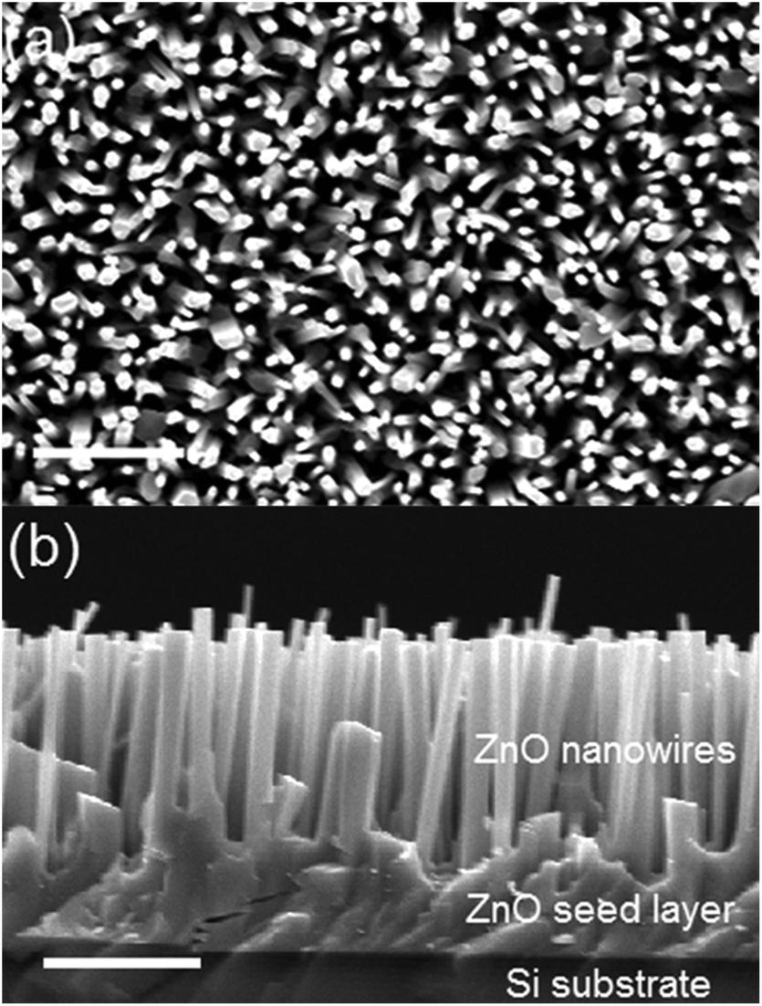 | ||
| Fig. 1 (a) Top-view, and (b) side-view SEM images of undoped ZnO nanowires grown on the ZnO seed thin film layer. The scale bar is 2 μm. | ||
The temperature-dependent photoluminescence (PL) measurement was performed with a 325 nm He–Cd laser for the as-grown ZnO nanowire sample to evaluate the optical properties. Fig. 2 shows PL spectra recorded at temperatures from 13 K to 290 K. From right to left there are four peaks around 3.361 eV, 3.305 eV, 3.233 eV and 3.163 eV in the spectra. The dominant emission peak at 3.361 eV is usually observed in the n-type ZnO and can be attributed to the donor bound exciton (D0X).19,20 The peak at 3.305 eV shows a slightly red shift with increasing temperature and therefore it is assigned to a free electron acceptor (FA).21,22 The chemical state of the acceptors may be related to unintentionally incorporated nitrogen species. The 3.233 eV peak is 72 meV at the lower energy side of the FA peak, which is equal to the phonon energy of ZnO, and thus it is attributed to the first phonon replica of FA (FA-1LO).23 Similarly, the obscure peak at 3.163 eV is 70 meV away from the FA-1LO peak and can be assigned to the second phonon replica of FA (FA-2LO). The observation of phonon replicas reveals the high quality of the ZnO nanowires.2,24
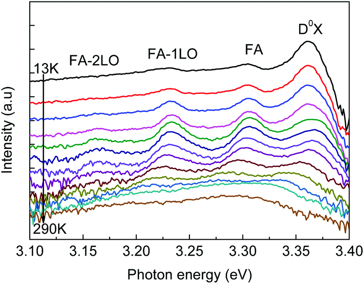 | ||
| Fig. 2 Temperature-dependent PL spectra of as-grown ZnO nanowires. The four peaks from left to right are assigned as FA-2LO, FA-1LO, FA and D0X, respectively. | ||
Fig. 3a shows a schematic of the device structure of the Schottky junction random laser diode. Au of 10 nm was deposited on top of the nanowires to form a Schottky junction at the interface. Due to the nanowire morphology, it is expected that Au will not be continuous as a thin film on the entire sample surface. While some Au form localized islands on each top ends of the nanowires, there is some metal leaking into void spaces in between the nanowires. Nevertheless, due to the limited Au evaporation and shade effect, the metal does not reach deep inside; instead it only coats the top portion of the nanowires. For each single nanowire, the Au on top forms a Schottky junction with the nanowire and the laser device can be treated as densely packed Au–ZnO Schottky junctions connected in parallel. The area of the device is about 1 cm by 1 cm. Device fabrication details are given in the Experimental section. Fig. 3b shows a current–voltage (I–V) curve in the dark. Rectifying behavior is observed. The relatively small turn-on voltage of about 0.7 V explains the formation of the Au–ZnO Schottky junction.25 As a reference, the I–V curve from a ZnO nanowire/thin film p–n junction is also shown in the ESI,† which exhibits different I–V characteristics with much larger turn-on voltage.
 | ||
| Fig. 3 (a) Schematic of the random laser device. The Schottky junction forms at the interface of each single ZnO nanowire and the Au “island” on top. The laser device is densely packed Au–ZnO Schottky junctions connected in parallel. (b) I–V curve of the Schottky device measured in the dark. | ||
Fig. 4a shows EL spectra of the Schottky diode laser device with increasing injection current under the forward bias. At currents below 60 mA, the EL spectra are dominated by a background noise. The EL near band edge spontaneous emission centered at around 385 nm superimposing with a few randomly distributed lasing modes starts to show up at a drive current of about 70 mA. Both spontaneous emission and lasing modes continue to grow stronger with the increase of the injection current. As the current reaches 100 mA (the corresponding voltage is 30 V), randomly distributed sharp peaks become dominating in the spectra. It is also noticeable that at an injection current of 100 mA peaks emerge between 320–335 nm and around 480 nm, which originates from the formation of Zn micro plasma generated in between ITO glass and some uncontacted nanowires as a result of the high electric field.26 The Zn plasma may contribute to the lasing process at 100 mA by re-absorption of some high-energy photons and subsequent generation of additional electron–hole pairs in ZnO. However, these peaks are not observed at lower voltages, effectively excluding Zn plasma being solely responsible for the lasing behavior in the device under lower biases. The inset in Fig. 4a is the photographic image of the random lasing device taken at a drive current of 100 mA. A very bright light spot with violet halo is obvious, which directly proves the lasing process in the Au–ZnO nanowire Schottky diode.
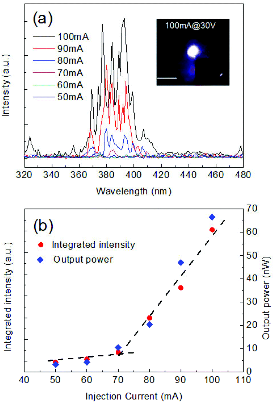 | ||
| Fig. 4 (a) EL spectra of the laser device operated at the drive current from 50 mA to 100 mA. Inset is the illumination photograph of the device driven at 100 mA and the scale bar is 1 cm. Zn plasma related peaks are evident in the spectrum as the device is driven by 100 mA. (b) Integrated intensity and output power as a function of injection current. Dashed line is a guide to the eye. | ||
Fig. 4b shows the integrated intensity and output power as a function of injection current. The output power was measured for a single wavelength of 385 nm from the normal to the surface of the device by using a Thorlabs PM100 Optical Power Meter. The integrated intensity was calculated by extracting the area under the random lasing spectra in between 360 nm and 420 nm at different injection currents, which matches reasonably well with the output power data trend. A dashed line is plotted to guide the eyes, showing a threshold current of about 70 mA. The output power is about 67 nW at a drive current of 100 mA, which is about two orders of magnitude higher than that of the MIS structure random laser device.18
Finally, we discuss the mechanism of the lasing behavior from the Au–ZnO nanowire Schottky diode. Fig. 5a shows a schematic of the simplified energy band diagram of the device. As a forward bias is applied on the Au metal, the energy band of ZnO bends downward adjacent to the metal–semiconductor interface. Electrons transport to the interface from the bulk of ZnO nanowires driven by an electric field. Under a sufficiently high forward bias, the sharply bent energy band region appears and holes can directly tunnel to the valence band of ZnO from the positive pole.27 These holes readily interact with electrons in the conduction band to form excitons and emit light through excitonic EL.28 Due to the limited hole injection, the exciton recombination process is believed to be responsible for the lasing behavior since population inversion is not necessary in excitonic lasing generation.29 The light is mostly generated in the nanowires below the Au/ZnO interface because of the small hole diffusion length.2 Light emits in all directions and the light path is complicated considering randomly distributed tilted nanowires. In some cases, the light can returns to where it starts; then close-loop resonant cavities for coherent lasing are formed,30,31 as schematically shown in Fig. 5b. When the light generation overcomes the loss inside the cavities, lasing signals start to dominate the EL spectra. As shown in Fig. 4a, the lasing peaks are from different lasing modes because the cavities are randomly formed.
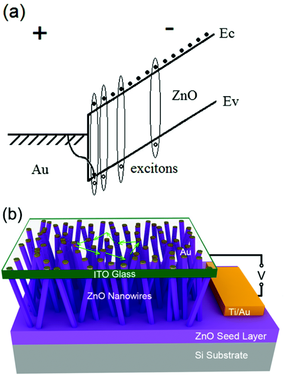 | ||
| Fig. 5 (a) Simplified band energy diagram of the Au–ZnO Schottky junction under the forward bias. The solid and hollow circles represent electrons and holes, respectively. (b) The formation of light close-loop cavity for random coherent lasing in the device. | ||
3. Experimental
Nanowire growth: an undoped ZnO seed layer of 1 μm was grown on a Si (100) substrate by plasma-assisted molecular-beam epitaxy. The ZnO/Si (100) sample was then transferred to a CVD furnace for vapor–solid growth of ZnO nanowires. The substrate was positioned at the center of the quartz tube. A silica bottle with zinc powder (99.999%, Sigma Aldrich) was placed 1 cm away from the substrate at the upstream side as a source material. A flow of 300 s.c.c.m. argon diluted oxygen (0.5%) was used as the reaction gas and a flow of 600 s.c.c.m. nitrogen was passed continuously through the furnace during the growth. The growth temperature is 515 °C and the growth duration is 40 min. The substrate was partly covered during the growth for subsequent contact formation on the ZnO film.Device fabrication: Ti/Au (10 nm/100 nm) contact was deposited on the ZnO thin film by e-beam evaporation. During the Ti/Au metal evaporation, the nanowires were protected by an aluminum foil. This metal contact was annealed at 400 °C for 60 seconds in a rapid thermal annealing (RTA) furnace to ensure Ohmic contact. Au of 10 nm was subsequently deposited on top of the nanowires for the formation of the Schottky junction. A slice of ITO glass was clamped on the device as a top contact where the ITO side connects the Au/ZnO nanowires for current feed through on the top contact of the Schottky diode random laser.
4. Conclusions
Undoped n-type ZnO bundle nanowires were grown on a ZnO seed thin film layer. The Au metal was deposited on the top ends of the nanowires to form a metal–semiconductor junction. The current–voltage curve in the dark indicates typical Schottky diode electrical characteristics. Good random lasing behavior is demonstrated, indicating that the leakage hole current flowing in a unipolar Schottky junction is sufficient to help trigger the excitonic process in ZnO nanowires, and initiate and maintain excitonic lasing. Furthermore, Zn plasma is only observed near 320 nm and 480 nm at a high current of 100 mA, and therefore differs from the random lasing spectral features in between 360 nm and 420 nm. This study demonstrates excitonic lasing through a nanowire Schottky diode, which provides an alternative device structure for the development of semiconductor random lasers.Acknowledgements
The authors acknowledge financial support from the Department of Energy (DE-FG02-08ER-46520), and the National Basic Research Program of China under Grant No. 2013CB932900 and 2011CB922100, NSFC under Grant No. 61205057 and 61204050, China Scholarship Council.References
- S. Chu, G. P. Wang, W. H. Zhou, Y. Q. Lin, L. Chernyak, J. Z. Zhao, J. Y. Kong, L. Li, J. J. Ren and J. L. Liu, Nat. Nanotechnol., 2011, 6, 506 CrossRef CAS PubMed.
- U. Ozgur, Y. I. Alivov, C. Liu, A. Teke, M. A. Reshchikov, S. Dogan, V. Avrutin, S. J. Cho and H. Morkoc, J. Appl. Phys., 2005, 98, 04301 CrossRef PubMed.
- J. B. Cui, Mater. Charact., 2012, 64, 43 CrossRef CAS PubMed.
- M. H. Huang, S. Mao, H. Feick, H. Q. Yan, Y. Y. Wu, H. Kind, E. Weber, R. Russo and P. D. Yang, Science, 2001, 292, 1897 CrossRef CAS PubMed.
- D. S. Wiersma, Nat. Phys., 2008, 4, 359 CrossRef CAS.
- B. Redding, M. A. Choma and H. Cao, Nat. Photonics, 2012, 6, 497 CrossRef.
- Q. H. Song, S. M. Xiao, Z. B. Xu, V. M. Shalaev and Y. L. Kim, Opt. Lett., 2010, 35, 2624 CrossRef PubMed.
- Q. H. Song, Z. B. Xu, S. H. Choi, X. H. Sun, S. M. Xiao, O. Akkus and Y. L. Kim, Biomed. Opt. Express, 2010, 1, 1401 CrossRef PubMed.
- D. S. Wiersma and S. Cavalieri, Nature, 2001, 414, 708 CrossRef CAS PubMed.
- R. C. Polson and Z. V. Vardeny, Appl. Phys. Lett., 2004, 85, 1289 CrossRef CAS PubMed.
- H. Zhou, M. Wissinger, J. Fallert, R. Hauschild, F. Stelzl, C. Klingshirn and H. Kalt, Appl. Phys. Lett., 2007, 91, 181112 CrossRef PubMed.
- S. Yu, C. Yuen, S. P. Lau, W. I. Park and G. C. Yi, Appl. Phys. Lett., 2004, 84, 3241 CrossRef CAS PubMed.
- H. C. Hsu, C. Y. Wu and W. F. Hsieh, J. Appl. Phys., 2005, 97, 4 Search PubMed.
- J. Huang, S. Chu, J. Y. Kong, L. Zhang, C. M. Schwarz, G. P. Wang, L. Chernyak, Z. H. Chen and J. L. Liu, Adv. Opt. Mater., 2013, 1, 179 CrossRef PubMed.
- Y. R. Ryu, J. A. Lubguban, T. S. Lee, H. W. White, T. S. Jeong, C. J. Youn and B. J. Kim, Appl. Phys. Lett., 2007, 90, 3 Search PubMed.
- H. K. Liang, S. F. Yu and H. Y. Yang, Appl. Phys. Lett., 2010, 96, 101116 CrossRef PubMed.
- F. Schuster, B. Laumer, R. R. Zamani, C. Magen, J. R. Morante, J. Arbiol and M. Stutzmann, ACS Nano, 2014, 8, 4376 CrossRef CAS PubMed.
- X. Y. Ma, J. W. Pan, P. L. Chen, D. S. Li, H. Zhang, Y. Yang and D. R. Yang, Opt. Express, 2009, 17, 14426 CrossRef CAS.
- X. Y. Liu, C. X. Shan, S. P. Wang, Z. Z. Zhang and D. Z. Shen, Nanoscale, 2012, 4, 2843 RSC.
- C. X. Shan, Z. Liu and S. K. Hark, Appl. Phys. Lett., 2008, 92, 073103 CrossRef PubMed.
- S. Karamat, R. S. Rawat, T. L. Tan, P. Lee, V. Springham, E. Ghareshabani, R. Chen and H. D. Sun, Appl. Surf. Sci., 2011, 257, 1979 CrossRef CAS PubMed.
- A. Teke, U. Ozgur, S. Dogan, X. Gu, H. Morkoc, B. Nemeth, J. Nause and H. O. Everitt, Phys. Rev. B: Condens. Matter, 2004, 70, 195207 CrossRef.
- J. N. Dai, H. C. Liu, W. Q. Fang, L. Wang, Y. Pu, Y. F. Chen and F. Y. Jiang, J. Cryst. Growth, 2005, 283, 93 CrossRef CAS PubMed.
- B. K. Meyer, H. Alves, D. M. Hofmann, W. Kriegseis, D. Forster, F. Bertram, J. Christen, A. Hoffmann, M. Strassburg, M. Dworzak, U. Haboeck and A. V. Rodina, Phys. Status Solidi B, 2004, 241, 231 CrossRef CAS PubMed.
- M. Asghar, K. Mahmood, F. Malik and M. A. Hasan, J. Phys.: Conf. Ser., 2013, 439, 012030 CrossRef.
- N. M. Shaikh, B. Rashid, S. Hafeez, Y. Jamil and M. A. Baig, J. Phys. D: Appl. Phys., 2006, 39, 1384 CrossRef CAS.
- P. G. Kasherininov, A. V. Kichaev and A. A. Tomasov, Semiconductors, 1995, 29, 1092 Search PubMed.
- H. Jeong, K. Min, S. Byun, C. J. Stanton, D. H. Reitze, J. K. Yoo, G. C. Yi and Y. D. Jho, Appl. Phys. Lett., 2012, 100, 02106 Search PubMed.
- J. W. Sun, Y. M. Lu, Y. C. Liu, D. Z. Shen, Z. Z. Zhang, B. H. Li, J. Y. Zhang, B. Yao, D. X. Zhao and X. W. Fan, J. Phys. D: Appl. Phys., 2008, 41, 15103 CrossRef.
- J. Fallert, R. J. B. Dietz, J. Sartor, D. Schneider, C. Klingshirn and H. Kalt, Nat. Photonics, 2009, 3, 279 CrossRef CAS.
- H. Zhu, C. X. Shan, J. Y. Zhang, Z. Z. Zhang, B. H. Li, D. X. Zhao, B. Yao, D. Z. Shen, X. W. Fan, Z. K. Tang, X. H. Hou and K. L. Choy, Adv. Mater., 2010, 22, 1877 CrossRef CAS PubMed.
Footnote |
| † Electronic supplementary information (ESI) available. See DOI: 10.1039/c5nr01349f |
| This journal is © The Royal Society of Chemistry 2015 |