
 Open Access Article
 This Open Access Article is licensed under a
 Creative Commons Attribution 3.0 Unported Licence
Gap and channeled plasmons in tapered grooves: a review
C. L. C.
Smith
a,
N.
Stenger
bc,
A.
Kristensen
a,
N. A.
Mortensen
bc and
S. I.
Bozhevolnyi
d
aDepartment of Micro- and Nanotechnology, Technical University of Denmark, DK-2800, Kgs. Lyngby, Denmark. E-mail: cameron.smith@nanotech.dtu.dk; anders.kristensen@nanotech.dtu.dk
bDepartment of Photonics Engineering, Technical University of Denmark, DK-2800, Kgs. Lyngby, Denmark. E-mail: niste@fotonik.dtu.dk; asger@mailaps.org
cCenter for Nanostructured Graphene (CNG), Technical University of Denmark, DK-2800, Kgs. Lyngby, Denmark
dInstitute of Technology and Innovation (ITI), University of Southern Denmark, DK-5230, Odense M, Denmark. E-mail: seib@iti.sdu.dk
First published on 12th May 2015
Abstract
Tapered metallic grooves have been shown to support plasmons – electromagnetically coupled oscillations of free electrons at metal–dielectric interfaces – across a variety of configurations and V-like profiles. Such plasmons may be divided into two categories: gap-surface plasmons (GSPs) that are confined laterally between the tapered groove sidewalls and propagate either along the groove axis or normal to the planar surface, and channeled plasmon polaritons (CPPs) that occupy the tapered groove profile and propagate exclusively along the groove axis. Both GSPs and CPPs exhibit an assortment of unique properties that are highly suited to a broad range of cutting-edge nanoplasmonic technologies, including ultracompact photonic circuits, quantum-optics components, enhanced lab-on-a-chip devices, efficient light-absorbing surfaces and advanced optical filters, while additionally affording a niche platform to explore the fundamental science of plasmon excitations and their interactions. In this Review, we provide a research status update of plasmons in tapered grooves, starting with a presentation of the theory and important features of GSPs and CPPs, and follow with an overview of the broad range of applications they enable or improve. We cover the techniques that can fabricate tapered groove structures, in particular highlighting wafer-scale production methods, and outline the various photon- and electron-based approaches that can be used to launch and study GSPs and CPPs. We conclude with a discussion of the challenges that remain for further developing plasmonic tapered-groove devices, and consider the future directions offered by this select yet potentially far-reaching topic area.
 C. L. C. Smith | Cameron Smith is a Postdoctoral Fellow with the Department of Micro- and Nanotechnology at the Technical University of Denmark. He completed his Bachelor of Electrical Engineering in 2005 and PhD in Nanophotonics in 2009 at the University of Sydney, Australia. Since moving to Denmark, he received a Marie Curie FP7 International Incoming Fellowship, and a Danish Council for Independent Research grant awarded with “Sapere Aude – Young Elite Researcher” honors. His current research interests include plasmonics, photonic crystals and optical sensors. |
 N. Stenger | Nicolas Stenger is an Assistant Professor with the Department of Photonics Engineering at the Technical University of Denmark. Previously, he received his MSc in 2004 and PhD in Condensed Matter Physics in 2008 from the University of Strasbourg, France, before embarking on invisibility cloaking research as a postdoctoral scholar at the Karlsruhe Institute of Technology, Germany. In 2012 he moved to Denmark and was awarded a fellowship from the Lundbeck Foundation to explore quantum effects in plasmonic graphene nanostructures. |
 A. Kristensen | Anders Kristensen is a Professor with the Department of Micro- and Nanotechnology at the Technical University of Denmark. He leads the Optofluidics group, which researches miniaturised sensing and actuator technologies. Prior to joining the faculty in 2001, he earned his PhD in Physics at the Niels Bohr Institute fAPG, University of Copenhagen, Denmark (1994), became a Research Fellow at the Physics Department of the University of London, UK (1994–1996) and later returned to Denmark as an Assistant/Associate Professor at the University of Copenhagen (1996–2001). |
 N. A. Mortensen | N. Asger Mortensen is a Professor (Dr Techn.) with the Department of Photonics Engineering at the Technical University of Denmark. His research group has a focus on wave phenomena and light-matter interactions in artificially structured materials and plasmonic nanostructures. After receiving his PhD in Theoretical Physics at the Technical University of Denmark (2001), he joined Crystal Fiber A/S as a research scientist (2001–2004) before returning to academia and becoming a faculty at the Technical University of Denmark in 2004. He is a Fellow of SPIE. |
 S. I. Bozhevolnyi | Sergey I. Bozhevolnyi is a Professor (Dr Scient.) with the Department of Technology and Innovation at the University of Southern Denmark, where he leads a Centre for Nano Optics. He received his PhD in Integrated Optics from the Moscow Institute of Physics and Technology, Russia (1981). He has been doing research in Denmark since 1991, working as Assistant/Associate/Full Professor at Aålborg University, Denmark (1992–2009). During 2001–2004, he was the Chief Technical Officer of Micro Managed Photons A/S. His current research interests include linear and nonlinear nano-optics, plasmonics and nanophotonics. He is a Fellow of the Optical Society of America. |
1 Introduction
Plasmonics represents a burgeoning subdiscipline of nanophotonics that considers the control of light at the nanoscale based on the nature of plasmons.1–6 Plasmons, considered here in the form of propagating surface-plasmon polaritons (SPPs), are oscillations of the free electron gas at metal–dielectric interfaces coupled to electromagnetic (EM) fields.6 These EM fields decay exponentially into the neighboring media, and through various techniques their distribution may be controlled to facilitate the concentration of light beyond its diffraction limit.7–11 Realizations of sub-diffraction-limited light have given rise to a host of scientifically and technologically significant optical components, including integrable ultra-compact photonic circuits,12–16 subwavelength nanolasers,17–21 quantum photonics devices,22–25 enhanced filters and structurally colored surfaces,26–30 nanoscale volume and single-molecule sensors,31–36 super-resolution nanoscopes and nanoprobes,37–41 and near-field traps for the manipulation of single molecules, atoms, and nano-objects.42–47The achievements rendered by plasmonics have been made possible by advances in fabrication techniques that can now routinely synthesize and pattern metals on the nanoscale.48–51 This is due to the fact that the topology and configuration of plasmonic nanostructures strongly determine the degree of EM field enhancement enabled by plasmons.10,11,52 In particular, the proximity between metal surfaces,53–58 the sharpness at the ends of tapered points,8,59–62 adiabatic scale transitions63–67 and the constituent materials involved68–72 all govern the degree of light confinement in space. Accordingly, a diverse set of structure types are pursued in order to nanofocus light, including nanoparticles,32,34,73,74 nanoholes,27,28,45,75 nanopatches,76–78 nanoantennas,79–82 nanowires,14,23,66,83 and an extensive list of planar waveguiding geometries.3,5,11,12
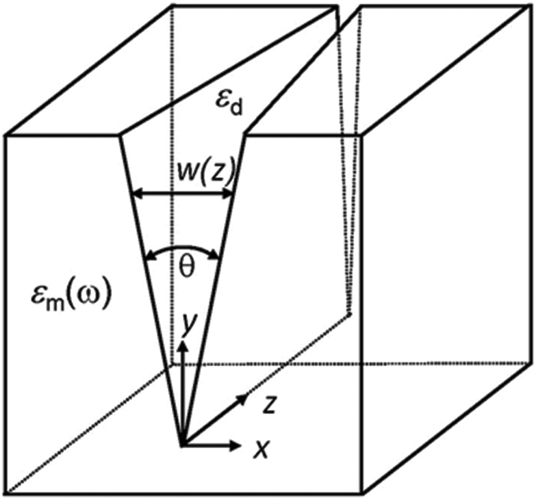
In this Review, we selectively consider the assortment of geometries and configurations of metallic tapered grooves that have been shown to support SPP-type modes;60,90–93 a sample of structures is displayed in Fig. 1.84–89Fig. 1(a) illustrates a representative tapered-groove – a V-shaped profile introduced into an otherwise planar metallic surface – with a plasmon propagating along the groove axis. The ensemble of plasmons supported by tapered grooves may be divided into two principal categories. First, gap-surface plasmons (GSPs),85,93–95 which are laterally confined modes between the tapered-groove sidewalls and may propagate either along the groove axis [Fig. 1(a)] or normal to the planar surface [Fig. 1(b)]. Second, channeled plasmon polaritons (CPPs),whose EM fields occupy the tapered profile and propagate along the groove axis;12,96–98Fig. 1(c) shows an example of a CPP mode obtained by a finite-element simulation (COMSOL Multiphysics) at telecommunications wavelengths. Fig. 1(d)–(j) highlight the variety of configurations of metallic tapered grooves so-far available, with the selection shown here offering new opportunities for strongly confined photonic circuitry,84 scientific studies of extreme EM field confinement,85 broadband light absorbers and polarizers,86 enhanced extraordinary optical transmission,87 UV-defined nanoplasmonic components with efficient plasmon excitation,88 and sophisticated nanoimprinted plasmonic waveguides.89
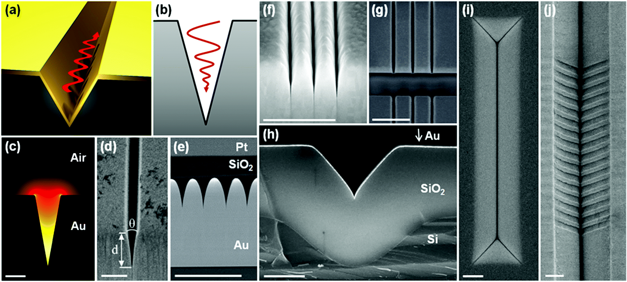 | ||
| Fig. 1 A variety of plasmonic tapered-groove geometries. (a) Illustration of a plasmonic tapered-groove, where a V-like channel is introduced into an otherwise planar metal surface. The red oscillating arrow depicts the propagation of a plasmon along the groove axis. (b) Schematic representation of a GSP propagating normal to the planar surface. (c) The normalized electric field distribution of a CPP mode solved by the finite element method at the free space telecommunications wavelength of 1.55 μm. (d)–(j) Scanning electron micrographs of assorted gold tapered-groove structures. (d) A FIB-milled tapered-groove with its end-facet at the edge of a gold slab.84 (e) A lamellar consisting of a set of tapered grooves used for studying extreme confinement behavior under electron energy-loss spectroscopy.85 (f) Efficient broadband light-absorbers given by a series of convex-shaped grooves.86 (g) Tapered periodic slits in a gold film for enhancing extraordinary optical transmission.87 (h) A tailored tapered-groove profile realized by oxidation of a anisotropically-defined silicon V-groove.88 (i) A similar device as shown in (h); waveguide termination mirrors form innate to the anisotropic process. (j) A Bragg grating filter in a plasmonic tapered-groove produced by nanoimprint lithography.89 All scale bars are 1 μm. (Adapted with permission from ref. 84–89 Copyright © 2011 Optical Society of America, © 2014 Macmillan Publishers Ltd, © 2013 American Institute of Physics, © 2011 IOP Publishing & Deutsche Physikalische Gesellschaft, © 2014 American Chemical Society, © 2012 Optical Society of America.) | ||
The aim of this Review is to introduce readers to the collection of plasmonic tapered-groove structure types so-far established and provide a research status update of their fundamentals, applications, synthesis and operation methods. We start in section 2 with a brief presentation of the theory and important features of GSPs and CPPs, highlighting the latest developments67,93 in the context of initial results.52,98–103 We outline the potential applications afforded by GSP and CPP characteristics in section 3, emphasizing recent reports on effective nanophotonic circuitry,84,89,104–108 efficient quantum emitter to plasmonic mode coupling,109–113 adiabatic nanofocusing,86,93,114–116 enhanced extraordinary optical transmission,87,95,117 resonant absorption118,119 and field enhancement,87,94,95,115,120,121 and nano-opto-mechanics.122 We follow in section 4 with an overview of the methods to fabricate plasmonic tapered grooves, concentrating on key results that now enable low cost, wafer-scale production of exceptional quality devices.88,89,91,123 We review in section 5 the existing techniques used to excite and study GSPs and CPPs, making a particular mention of direct, normal illumination arrangements that yield high plasmon launch efficiencies using waveguide termination mirrors,88,92 and electron-based approaches that have yielded new insights into optically dark modes of nano-scale structures via electron energy-loss spectroscopy (EELS).85 We discuss in section 6 the challenges that remain for further developing tapered-groove-based devices, noting that recent work elucidating non-local effects124,125 and the presence of antisymmetric modes85 represent potentially crucial factors that should be accounted for in device design. The Review concludes in section 7 with an outlook of the future directions offered by this rapidly advancing topic area.
The ensuing section headings are as follows:
Section 2: Plasmons in tapered grooves: fundamentals
Section 3: Plasmons in tapered grooves: applications
Section 4: Fabrication
Section 5: Excitation and characterization
Section 6: Challenges
Section 7: Outlook
2 Plasmons in tapered grooves: fundamentals
In this section we present the fundamental physics and important features of SPP-type modes in tapered grooves. We consider two principal categories: GSPs and CPPs, for which both may be described as EM modes that exist within the interior of the metallic V-like profiles. Of these, we first cover GSPs – plasmons in metal–insulator–metal (MIM) type configurations – which may either propagate along the tapered-groove axis [Fig. 1(a)], or normal to the planar surface [Fig. 1(b)]. We then follow with CPPs, a subset of GSP eigenmodes propagating along the tapered-groove axis, which consist of EM fields occupying the V-like profile [Fig. 1(c)]. We distinguish between GSPs and CPPs propagating along the groove by their EM distributions: GSPs may be locally excited such that the difference in spacing of the gap in the vertical direction is negligible, whereas CPP modes necessarily experience the gap-width variation of the tapered-groove shape. Nevertheless, GSPs and CPPs are both SPP-type modes, so before proceeding we summarize the relevant elements of SPPs.2.1 Surface-plasmon polaritons
SPPs are modes bound to and propagating along a metal–dielectric interface consisting of transverse magnetic EM waves (electric field oriented along the y-axis) that decay exponentially into both the metal and dielectric media9,126 (Fig. 2). The tangential field components (along the z-axis) are continuous across the interface and correspond to the wavevector kz such that the SPP electric fields can be written as follows: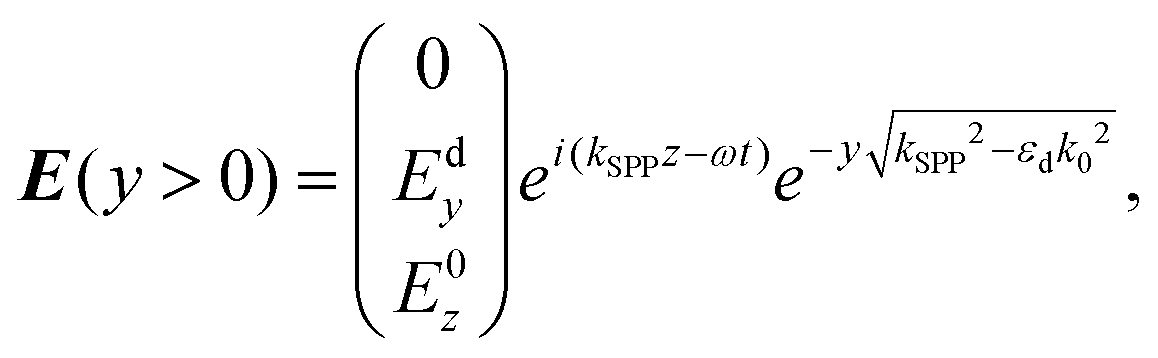 | (2.1a) |
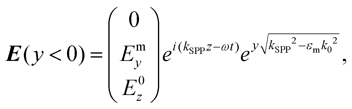 | (2.1b) |
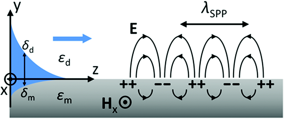 | ||
| Fig. 2 Illustration of the field components of a SPP supported by a metal–dielectric interface. The mode is transverse magnetic, exhibiting electric field components normal to the interface (y-axis) and along the propagation direction (z-axis). The mode profile (blue) represents the magnitude of the corresponding magnetic field, itself oriented along the x-axis, as a function of y. | ||
The SPP EM waves are coupled to the free electrons of the metal surface and give rise to collectively oscillating charge separations that correspond to the EM fields. Since the electric field components should satisfy Coulomb's law ∇E = 0, transverse electric EM waves (electric field oriented along the x-axis) cannot couple to the tangential electron oscillations along the z-axis at the metal surface and form SPPs. The normal field components (along the y-axis) can then be written in terms of the mutual tangential component:
 | (2.2a) |
 | (2.2b) |
By using the boundary condition εdEdx = εmEmx, the SPP dispersion relation can be found:
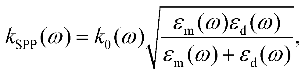 | (2.3) |
The SPP propagation constant relates to the effective refractive index of the SPP mode by Neff = kSPPλ/(2π), with the real and imaginary parts determining the SPP wavelength, λSPP = 2π/Re{kSPP}, and the intensity-based propagation length, LSPP = 1/Im{2kSPP}. We can see that the SPP wavelength is shorter than the light wavelength in the dielectric, and using the free-electron (Drude) approximation for the metal permittivity, εm(ω) = 1 − (ωp/ω(ω + iγ))2 where ωp is the plasma frequency and γ is the damping coefficient of the electron oscillations, the SPP wavelength approaches zero at the high frequency (short wavelength) limit of the dispersion relation, i.e. when 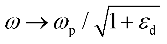 .6,53,126 The propagation length is also an important factor for SPP-based devices since it is significantly limited by γ as a result of Ohmic dissipation. This leads to short propagation lengths that restrict the available length-scales for realizing SPP-based devices, and may otherwise generate unwanted heat. Nevertheless, there are major efforts to address plasmonic losses,127,128 (together with critical discussions on the topic)129,130 and the efficient conversion of EM fields to heat via plasmons has been harnessed to great effect across a variety of configurations.47,131,132
The SPP amplitudes of the normal and tangential electric field components in the dielectric and metal can be explicitly related as follows [eqn (2.2a) and (2.2b)]:
 | (2.4a) |
 | (2.4b) |
Generally, metals have large magnitudes of the dielectric permittivity such that |εm| ≫ εd, resulting in the normal component being greater in the dielectric and the tangential component being greater in the metal. This is representative of the hybrid nature of SPPs, which consist of EM waves propagating through the dielectric and free-electron oscillations in the metals.133 We remark here that since the damping of SPPs is primarily caused by Ohmic dissipation in the metal, the tangential electric field component is therefore the determining factor of loss in SPPs.5
The penetration depth of the SPP electric fields (distance from the interface where the field amplitude decreases to 1/e of its value at y = 0) into both the dielectric δd and metal δm are different, as given by eqn (2.1a) and (2.1b). Together with the dispersion relation [eqn (2.3)], δd(m) is found to be:
 | (2.5) |
| δd ≈ (λ/2π)2(ωp/cεd), | (2.6a) |
| δm ≈ c/ωp. | (2.6b) |
The above relations [eqn (2.5) and (2.6a, 2.6b)] can be used to estimate the fraction of the SPP electric field in the dielectric as being proportional to (|εm|/εd)2,5 which at a first glance may seem surprising from a photonics perspective, since typically light experiences greater confinement within dielectric regions of higher refractive index. This trait of SPPs indicates that the electric field increases its overlap with the metal for shorter wavelengths, and therefore dielectrics of higher refractive index result in a shorter SPP propagation length and a reduced penetration depth, εd.
We note here that this brief subsection on SPPs has only summarised the details relevant to the topics of the Review. More detailed information can be found throughout the comprehensive set of literature available.3,5,9–11,126,134–136
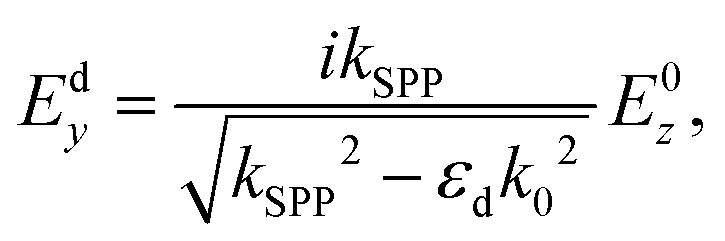
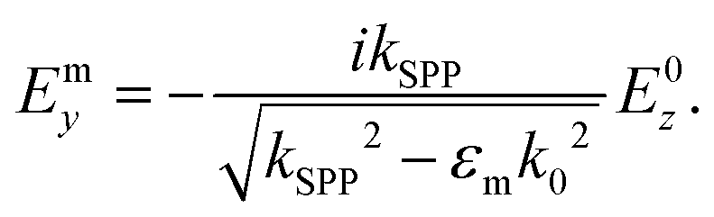
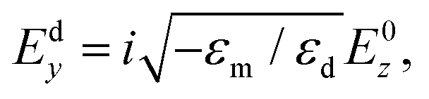
2.2. Gap-surface plasmons
We now consider SPP modes in the MIM configuration consisting of two close metal surfaces of the same material separated by a dielectric gap of width w (Fig. 3). For sufficiently small gap widths, the SPPs associated with the two metal surfaces may interact with each other and form single GSPs, in which the fundamental symmetric eigenmode exhibits odd symmetry of the tangential electric field component, Ez, and an even symmetry of the normal field component, Ey. This configuration, often called the plasmonic slot waveguide, has sparked an extensive research interest with regards to planar photonic integration12,97,138 due to the possibility it offers for achieving strong mode confinement together with relatively low Ohmic dissipation57,139 and bend loss.140 | ||
| Fig. 3 Illustration and numerically-solved field components of a symmetric GSP mode propagating along the z-axis supported by two metal surfaces with a dielectric gap of width w between. The corresponding electric field has its normal component, Ey, maintaining the same sign across the gap with an even-symmetric profile, whereas the tangential component, Ez, consequently exhibits an odd-symmetric profile. The calculated electric fields were obtained with the aid of finite-element method simulations (scale normalized for clarity) using gold surfaces with an air gap of width w = 0.5 μm at λ = 775 nm (nm = 0.174 + 4.86i).137 | ||
The GSP mode effective refractive indices and their corresponding propagation lengths were numerically solved (Fig. 4) as a function of gap width for light wavelengths selected between the visible and telecommunications.101 A major feature of the symmetric GSP is that its propagation constant, kGSP, increases indefinitely as the gap width approaches zero, indicating that the mode can be indefinitely squeezed in its lateral cross-section, albeit at the cost of generally increasing losses. It is interesting to note that the GSP propagation length first increases when the gap width decreases from large values that correspond to uncoupled separate SPPs. This may seem counter intuitive at first, since it implies that GSP modes with greater confinement may experience longer propagation lengths.101 The inset of Fig. 4 shows that the longest propagation length, LGSP, is ∼8% larger than the individual SPP propagation length, LSPP, (w → ∞). The optimal gap width in this respect can be explained as the two electric field components of the GSP, Ey and Ez, approaching the electrostatic (capacitor) mode, where the larger component, Ey, is constant across the gap. Here, the fraction of the electric field energy located in the gap region first increases (lossy component in the metal decreases) as w decreases, before reaching its maximum and then decreasing as the field is squeezed from the gap into the metal. As such, the GSP configuration may optimally exploit the available dielectric space of the gap region to minimize dissipative losses in the metal.
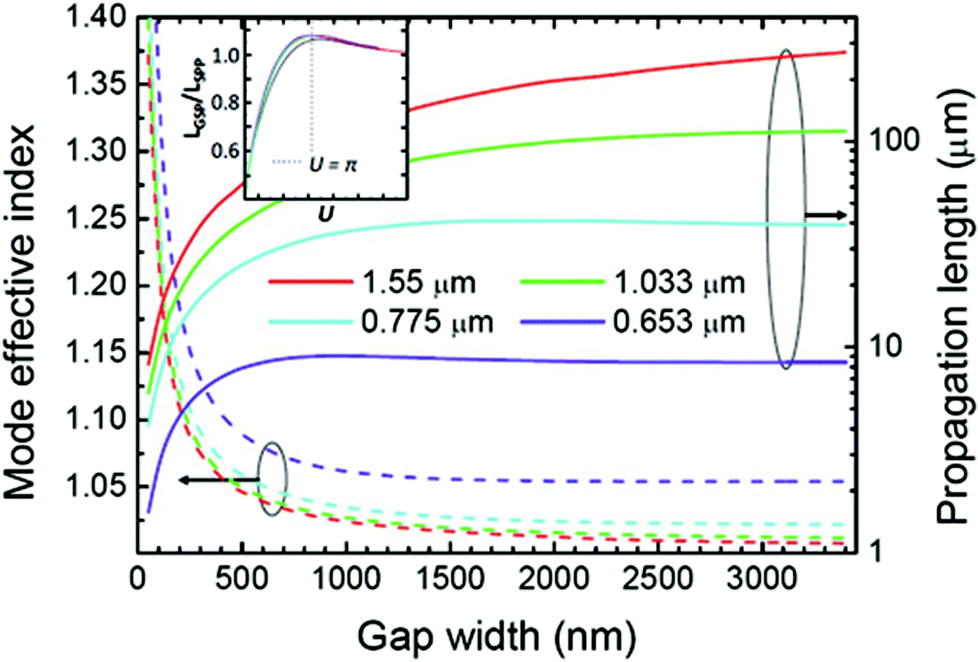 | ||
| Fig. 4 The GSP mode effective refractive index and its propagation length as a function of the width, w, of the gap region (air) between the metal (gold) surfaces for several light wavelengths.101 Under certain conditions, the propagation length may increase for decreasing gap width. Inset: the ratio of the GSP and SPP propagation lengths, LGSP/LSPP, as a function of the normalized gap width, u = kdyw.98 (Adapted with permission from ref. 98 and 101 Copyright © 2006 Optical Society of America, © 2007 Springer.) | ||
Applying the appropriate boundary conditions of the electric field components for SPPs and the configurations of symmetry described above, the dispersion relation for kGSP may be derived53,141,142
 | (2.7) |
Table 1 summarizes several analytical approximations for kGSP under different conditions of the gap width, w.98,103 For the small-gap approximation, k0GSP = −(2εd)/(wεm), which represents the GSP propagation constant for vanishing gaps (w → 0). Here, the real part of the corresponding effective refractive index, Re{kGSPλ/(2π)}, becomes much larger than the dielectric refractive index, while the imaginary part also increases. For larger gaps where the two SPP modes barely interact, the first-order corrected expression is given, where higher-order corrections may be carried out by iterating the values for kGSP into the normal wavevector component  and recalculating kGSP.98
| Gap width | Condition | Approximation | Analytical expression |
|---|---|---|---|
| Small | w → 0 | tan![[thin space (1/6-em)]](https://www.rsc.org/images/entities/char_2009.gif) h x ≈ x h x ≈ x |

|
| Large | Individual SPPs start to interact | tanh x ≈ 1 − 2exp(2x) |
|
| Moderate | w > (λεd)/(π|εm|) | tanh x ≈ x |
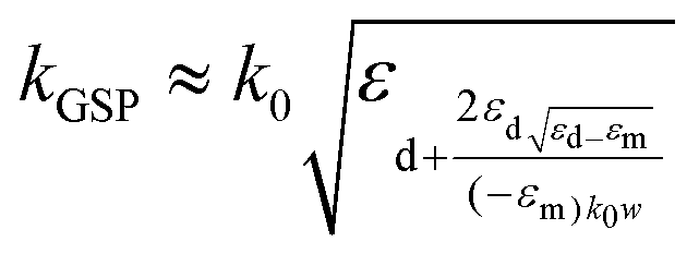
|
Using the large-gap approximation and evaluating kGSP with only the major electric field components, the normalized fraction of the electric field energy inside the gap can be expressed as a function of the normalized gap width, u = kdyw:
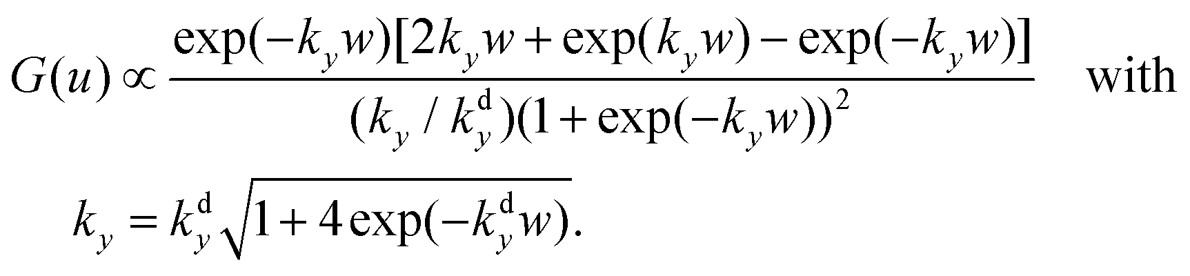 | (2.8) |
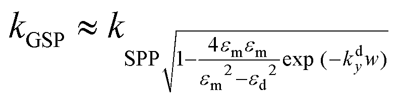
This function reaches its maximum value, 6% larger than w → ∞, at u ≈ 3.48, resulting in the following expression for the optimum gap width: wopt ≈ 0.5λ|Re{εm} + 1|0.5. It is interesting to note that the condition ensuring longest GSP propagation length is close to u = π (inset of Fig. 4), which resembles the resonator condition where kdy is the wave-vector component in the dielectric pointing across the gap.98
If the different gap-dependent terms in the small-gap approximation are considered, then the GSP propagation constant may be approximated for moderate gap widths, defined as |k0GSP|〈k0 ⇔ w〉(λεd)/(π|εm|). The GSP mode effective refractive indices and propagation lengths are plotted as a function of the gap width in Fig. 5. As before, several wavelengths spanning from visible to telecommunications regimes are considered, using both the exact dispersion relation from eqn (2.7) and the moderate-gap approximation.103 The validity of the moderate-gap approximation and its applicability for analyzing various GSP configurations has been demonstrated in work exploring the plasmonic analogs of black holes58 and, as will be discussed below, the adiabatic nanofocusing of radiation in narrowing gaps.67,143,144
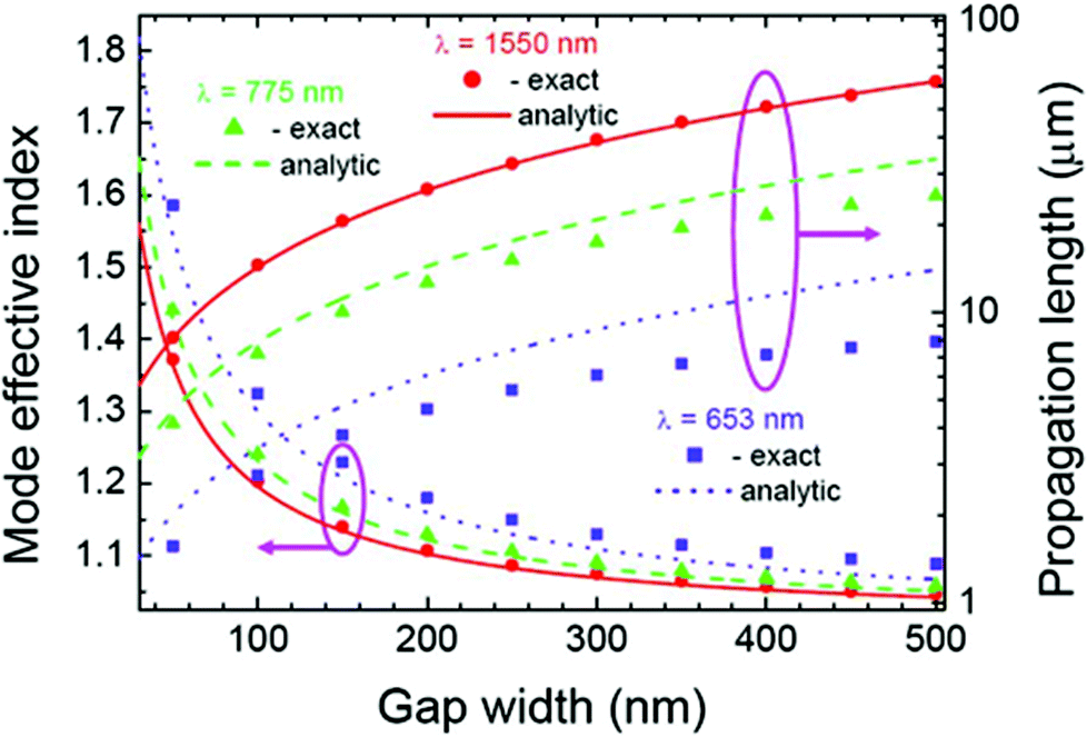 | ||
| Fig. 5 The GSP mode effective refractive index and its propagation length as a function of the width of the gap region (air) between the metal (gold) surfaces for several light wavelengths calculated exactly [eqn (2.7)] and using the analytical moderate-gap approximation (Table 1). (Reprinted with permission from ref. 103 Copyright © 2008 Optical Society of America.) | ||
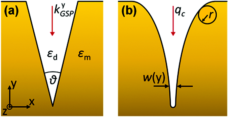 | ||
| Fig. 6 Parameters defining plasmonic V-grooves consisting of (a) linear (b) convex-shaped tapers for GSPs propagating normal to the planar surface (along the y-axis). ((b) is adapted from ref. 93 Copyright © 2012 Macmillan Publishers Ltd.) | ||
The adiabatic parameter may be described mathematically as63,145
 | (2.9) |
| δ(y) ≲ 1. | (2.10) |
In the continuous-matter approximation, the adiabatic parameter δ(y) reaches its maximum (finite) at the (infinitely) sharp tip of a linear taper.145–147 Accordingly, if the adiabatic condition is held at the tip, it will be satisfied everywhere.145,146 Assuming the above relation (2.10) is valid, and using asymptotic analysis for the GSP propagation near the structure's tapered end (tip), the following analytical expression can be found for the critical taper angle:145,146
| θc ≈ −2εd/Re{εm}. | (2.11) |
For tapered geometries consisting of a taper angle below the critical angle, θ < θc, the adiabatic condition holds.
As an example, let us consider a GSP propagating vertically towards the bottom of a gold V-groove in air with a taper angle θ. Using eqn (2.11), a light wavelength of λ = 775 nm results in a critical taper angle of θc ≈ 5°, and for λ = 1550 nm it is θc ≈ 1°. Such narrow V-grooves with straight sidewalls can be difficult to produce in practice, however, and results on V-grooves of larger taper angles (θ > 10°) report resonant GSP nanofocusing, where reflection from the groove sidewalls is significant (i.e. not adiabatic) and becomes an important aspect of the local field enhancement.87,94,148
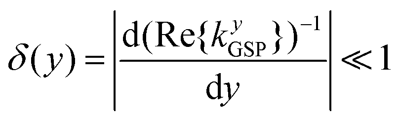
In order to explore the adiabatic condition further, the moderate-gap approximation can be rewritten in the following form:149
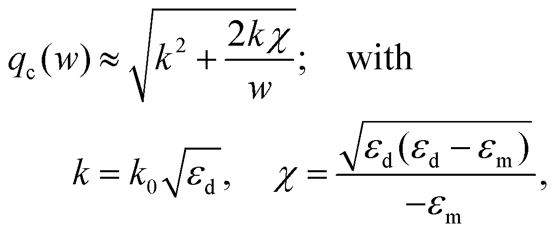 | (2.12) |
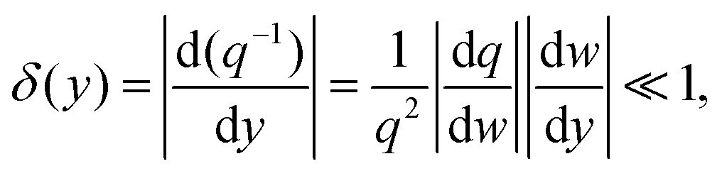 | (2.13) |
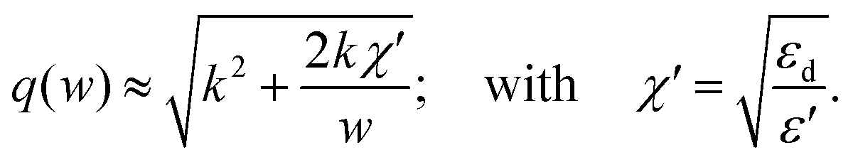 | (2.14) |
By using eqn (2.14) for the adiabatic condition expressed in eqn (2.13) for the limit of w(y) → 0 (where variations of q become strong), the final representation of the adiabatic condition can be obtained, given as93
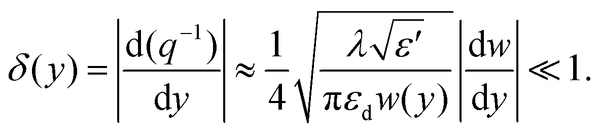 | (2.15) |
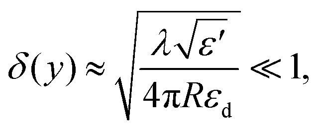
This relation implies that, in the case of linear V-grooves [Fig. 6(a)] where dw/dy = constant, the adiabatic condition must inevitably break down near the groove bottom as the groove width becomes sufficiently small, causing resonant behavior and GSP reflection.87,94,148 However, the condition may be satisfied for the entire groove depth under the configuration of convex-shaped grooves [Fig. 6(b)], where the groove walls become parallel at the contact point much like the case of touching cylinders.58 In the case of cylinders of equal radii R, the adiabatic condition reduces to93
 | (2.16) |
2.3 Channel-plasmon polaritons
We now consider the class of GSP eigenmodes that propagate along the tapered-groove axis: CPPs. From an effective index method (EIM) perspective,101 the tapered groove can be represented as a stack of infinitesimally thick MIM waveguides, each with a positional-dependent insulator width, w(y), between a top dielectric layer and bottom metal layer. The local GSP effective refractive index of each stack is determined by its w(y), increasing towards the bottom of the groove and resulting in confinement of the CPP mode to within the structure.The CPP effective refractive index increases and the propagation length correspondingly decreases as the groove angle, θ, is reduced (Fig. 7).97,101,152 The CPP mode effective refractive index, Neff, determines the mode confinement since the mode penetration depth in the dielectric is given by δd = (λ/2π)(Neff2 − 1)−0.5. Similar to the SPP, the CPP mode is more tightly confined to the metal (bottom of the groove) when Neff is larger, and also when the groove angle is narrower. The result of this means yet further mode confinement for progressively smaller tapered-groove cross-sections98 – a feature made possible by the nature of plasmons – although at the cost of larger Ohmic losses. One can also see that the CPP propagation length starts to rapidly increase when the decreasing groove depth reaches a certain (cut-off) value, below which no CPP modes exist. Here, the CPP mode effective refractive index approaches that of the dielectric and corresponds to the extension of the CPP mode profile progressively out of the groove.
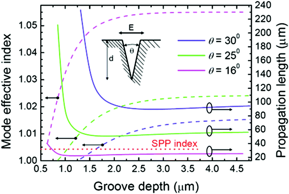 | ||
| Fig. 7 The effective refractive indices of fundamental CPP modes at λ = 1.55 μm and their propagation lengths as a function of the groove depth for different groove angles, θ. The insert shows the groove configuration and dominant orientation of the CPP electric field. The planar SPP effective refractive index is also included. (Reprinted with permission from ref. 101 Copyright © 2006 Optical Society of America.) | ||
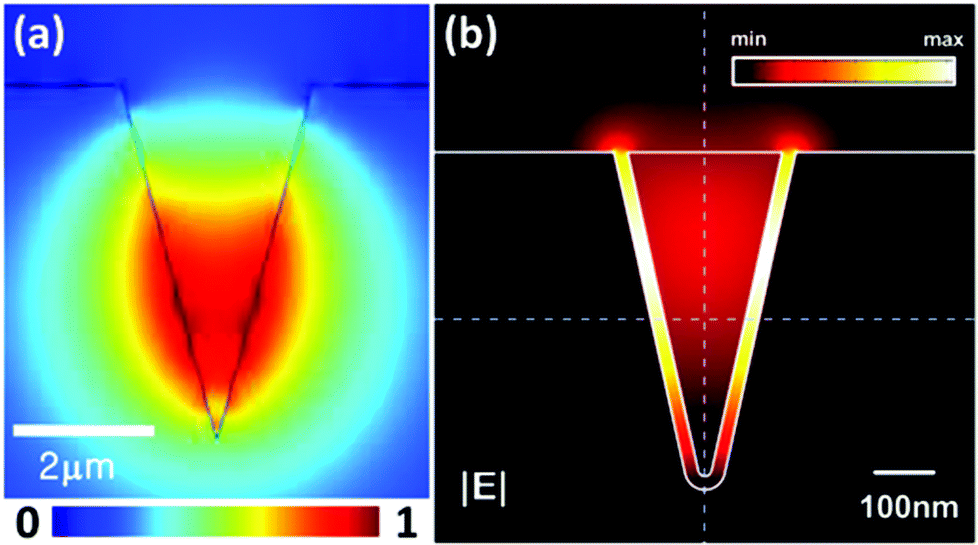
Using the finite-element method (COMSOL Multiphysics), we numerically solve the CPP mode for a gold V-groove in air (tip rounding curvature radius: 5 nm) at a light wavelength of λ = 1.55 μm (nm = 0.55 + 11.5i) and plot various electric field components in Fig. 8. The dominant component of the electric field, Ex, is essentially perpendicular to the metal sidewalls which corresponds to the expected behavior of individual SPPs on planar surfaces [Fig. 8(a)]. Like SPPs and GSPs, CPPs also possess a component in the direction of propagation, Ez, where Fig. 8(b) shows an antisymmetric profile about the V-groove geometry and represents the capacitor-like charge distribution of the mode. The overall normalized magnitude of the CPP electric field, |E|, is given in Fig. 8(c) together with the logarithmically-scaled electric field strengths (black arrows) in the xy-plane. One can readily see that the whole CPP mode closely resembles the distribution of Ex, although locations near the opening corners (rounding curvature radii: 50 nm) are comprised of significant Ez (and Ey) components since Ex is not supported by the parallel surface plane.5
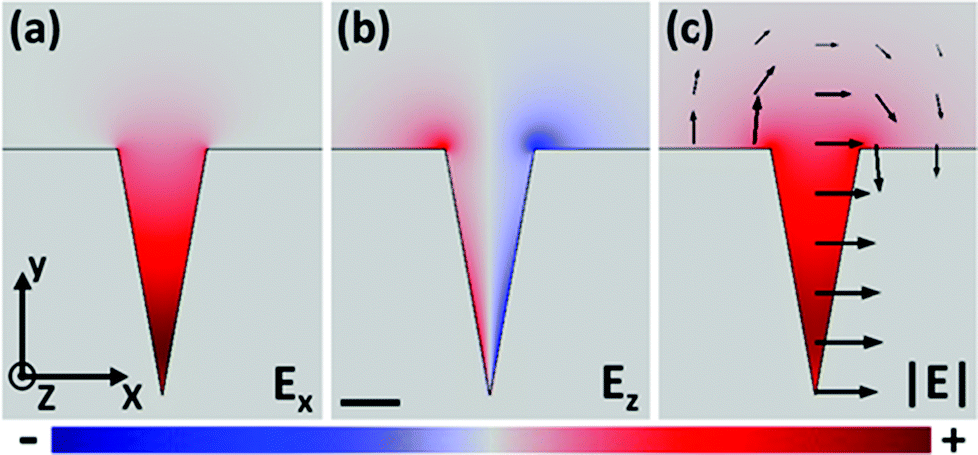 | ||
| Fig. 8 A CPP mode calculated via finite-element method for a gold V-groove in air at λ = 1.55 μm. (a) The dominant electric field component, Ex, points across the groove. The scale bar is 1 μm. (b) The electric field component oriented along the direction of propagation, Ez, highlights the antisymmetric (i.e. capacitor-like) charge distribution of the CPP mode. The field amplitude scales for Ex and Ez in (a) and (b) are normalized for clarity; the true maximum of Ex in (a) is significantly greater. (c) The magnitude of the normalized electric field component, |E|, represents the resulting CPP. Here, the mode closely resembles the distribution of Ex, although regions located near the opening corners (wedges) are comprised of significant Ez (and Ey) components. The arrows represent the electric field lines in the xy plane. | ||
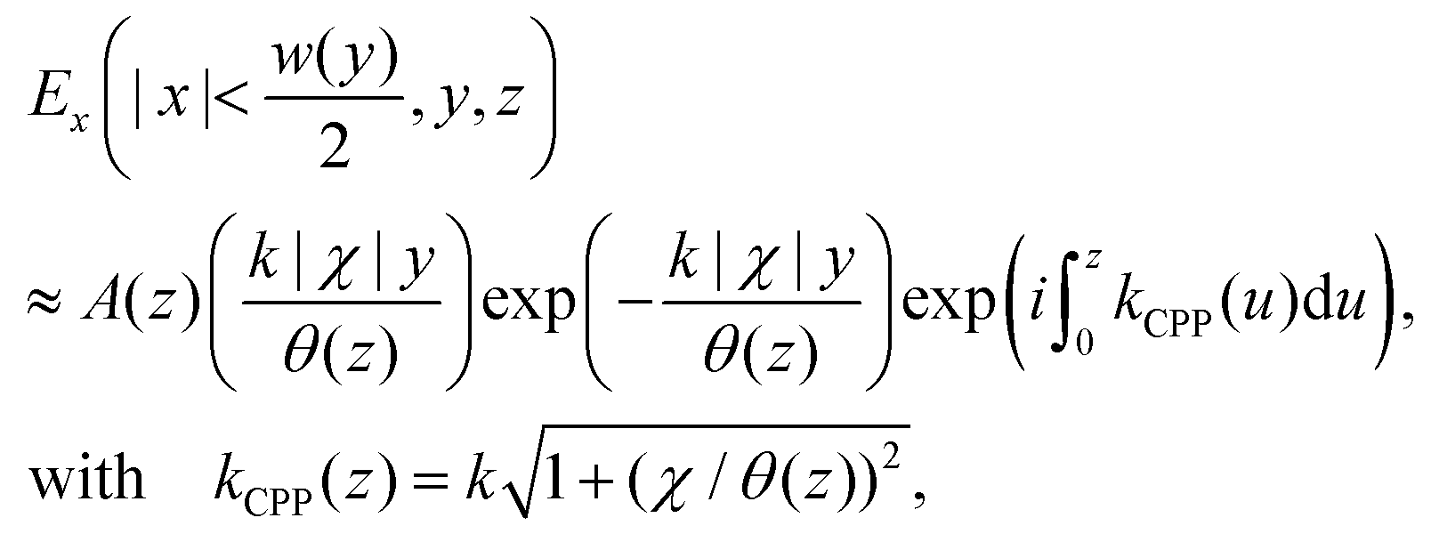
The EIM approach has been shown to provide sound qualitative and quantitative insights into the behavior of CPPs,153 offering the advantage of simplicity over preceding work (i.e. Green's theorem first in the electrostatic limit99 and then later for propagating modes).100 Taking this further, and in conjunction with the explicit expression for the propagation constant of the moderate-gap approximation (Table 1), the EIM framework was used to derive useful analytic formulas for CPP mode distributions143,149 in the form of
| Ex(x, y, z) = X(x, y)Y(y)exp(ikCPPz), | (2.17) |
 | (2.18) |
 | (2.19) |
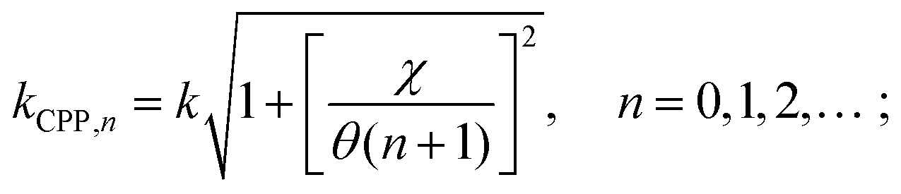
Eqn (2.18) and (2.19) have been used to calculate the CPP mode distributions for gold V-grooves in air (Fig. 9),149 reflecting the influence of groove angle and light wavelength (nm = 0.272 + 7.07i at 1.033 μm), and bearing a close resemblance to those calculated numerically.52,154,155 The CPP mode profiles and propagation constants can, on one hand, expect to be similar for finite-depth grooves provided that the planar surface occurs sufficiently far away from the mode maximum. On the other hand, a cut-off depth where CPP modes are no longer supported can be evaluated as a function of the position of the mode maximum for the fundamental CPP mode, using the following condition as a normalized depth coordinate ξco = k|χ|d/θ > 1, where d is the depth of the groove. Alternatively, this condition may be conveniently expressed by making use of the normalized waveguide parameter, VCPP:103,143,149
 | (2.20) |
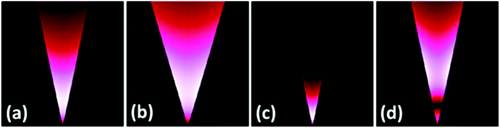 | ||
| Fig. 9 (a)–(c) Fundamental and (d) second CPP mode field magnitude distributions for gold V-grooves in air obtained using eqn (2.18) and (2.19) for different groove angles: (a, c, d) θ = 25° and (b) θ = 35°, and wavelengths: (a, b) λ = 1.55 μm and (c, d) λ = 1.033 μm. All panels have a lateral size of 6 μm. (Adapted with permission from ref. 149 Copyright © 2009 Optical Society of America.) | ||
The cladding material filling the V-groove also plays a role in the plasmonic mode distribution, for which an increase of its dielectric permittivity, εd, has been shown to result in a rapid increase of the mode localization to the bottom tip of the groove [Fig. 10(a)] and larger critical angles where CPP modes can exist.102,160 This behavior corresponds to the similar physics governing the penetration depths of SPPs, δd(m) in eqn (2.5), where a larger εd results in a larger electric field overlap with the metal, δm. Although the CPP Ohmic losses are greater for larger εd, designing tapered grooves with cladding materials other than air represents potentially important findings with regards to e.g. relaxed tapered-groove fabrication criteria, applications related to sensing or other lab-on-a-chip (LOC) devices, and efforts regarding gain-assisted loss compensation.128
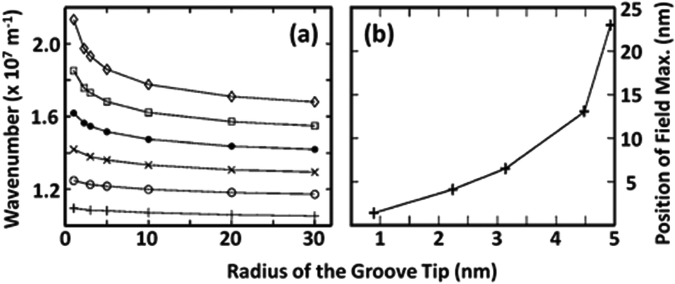 | ||
| Fig. 10 CPP mode dependencies for a silver V-groove in air at λ = 632.8 nm, εm = −16.22 + 0.52i, as a function of tip radius. (a) The CPP wavenumber for a groove angle of θ = 30° for different values of the dielectric permittivity in the groove: εd = 1 (+), εd = 1.21 (○), εd = 1.44 (×), εd = 1.69 (●), εd = 1.96 (□), and εd = 2.25 (◊). (b) The location at which the maximum of the CPP field occurs away from the tip into the dielectric (along the z coordinate) for a groove angle of θ = 45°. (Adapted with permission from ref. 102 Copyright © 2008 American Institute of Physics.) | ||
A significant parameter to account for is the finite corner rounding at the bottom tip of the groove, which profoundly affects the CPP mode profile and necessarily occurs in all practically fabricated devices. It was shown numerically that less-sharp corners result in less tightly confined modes (Fig. 10),102 indicating that corner rounding increases the penetration depth into the dielectric for progressively larger radii of curvature. The phenomenon can be related to locally reducing gap widths towards the groove bottom that, as with the case of GSPs, result in larger values for Neff and therefore tighter mode confinement. The results of ref. 102 stress the importance of having a close estimate of the corner rounding (e.g. ∼5 nm)88 and also highlight the need for including finite rounding values in numerical models since infinitely sharp points lead to non-physical singularities (within the local-response approximation).125
It is worth mentioning here that the position of the electric field maximum for the CPP is not located at the very bottom of the groove [Fig. 10(b)], but is instead located slightly above. This spatial shift is due to the finite corner rounding, which may seem unexpected since the gap still reduces towards the tip. The shift can be explained by successive reflections from the tip of the groove and the turning point (simple caustic),145 which occurs when the plasmon experiences non-adiabatic focusing: i.e. when the groove angle is larger than the critical taper angle, θ > θc,102,145 as discussed earlier.
 | (2.21) |
 . For gold V-grooves in air at telecommunications wavelengths, this condition results in θ > θmin ≈ 2°.
 | ||
| Fig. 11 Geometry of a tapered groove whose angle, θ, reduces along the groove axis. (Adapted with permission from ref. 67 Copyright © 2010 Optical Society of America.) | ||
Using the approximations given in ref. 67 and the CPP power dissipating according to γ(z), the CPP intensity, normalized to the value at the beginning of the taper, can be expressed as follows:
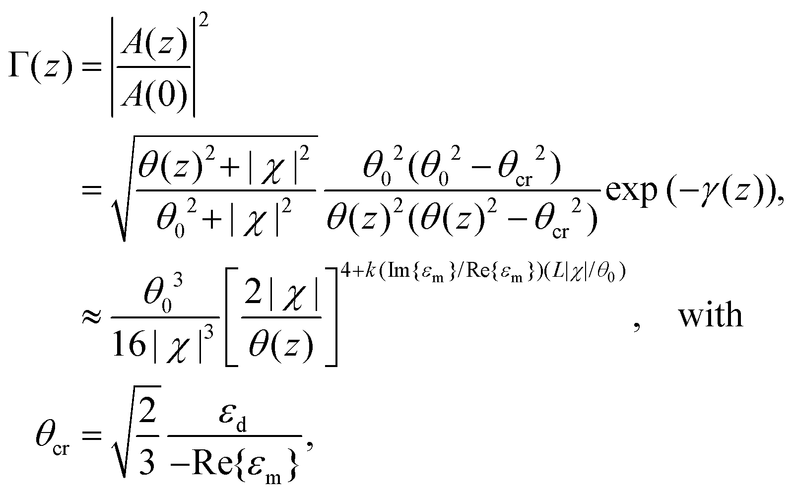 | (2.22) |
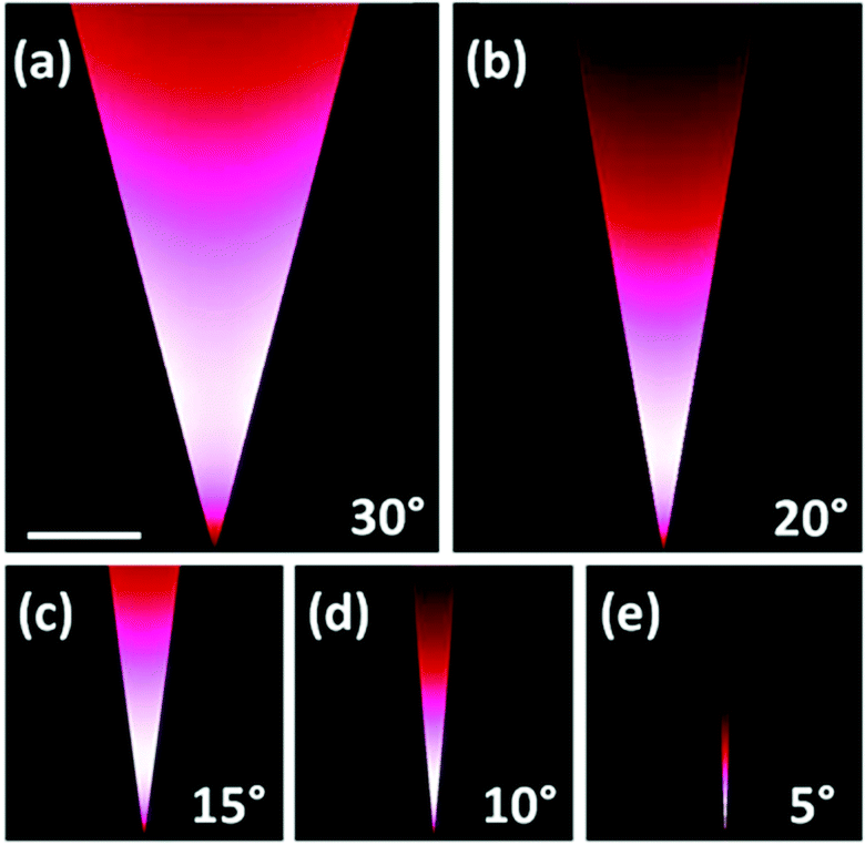 | ||
| Fig. 12 Fundamental CPP mode field magnitude distributions calculated for gold V-grooves in air at λ = 1.55 μm with varying groove angles: θ = (a) 30°, (b) 20°, (c) 15°, (d) 10°, (e) 5°. The scale bar in (a) represents 1 μm. (Adapted with permission from ref. 67 Copyright © 2010 Optical Society of America.) | ||
The approximate expression of (2.22) provides straightforward access to a fundamental characteristic of any nanofocusing configuration, namely the critical taper length, Lcr, at which the focusing and dissipation effects are balanced. Considering the case described above, useful enhancement of the CPP mode intensity can be achieved for taper lengths L < Lcr ≈ 4(−Re{εm}/Im{εm})(θ0/k|χ|),67i.e. Lcr ≈ 62 μm at λ = 1.55 μm. It is noteworthy that for λ = 1.033 μm, Lcr ≈ 31 μm, signifying the strong wavelength dependence on the relevant length-scales for achieving adiabatically nanofocused CPPs.
3 Plasmons in tapered grooves: applications
In this section we cover the potential applications offered by plasmons in tapered grooves. Their properties as described in section 2 are often investigated in the context of information-based technologies, where the subwavelength confinement of optical modes offers the possibility to facilitate extremely compact, high performance photonics components84,89,104–107 and effective platforms to realise quantum-plasmonics technologies.109–113 However, an increasing list of other types of tapered-groove-based devices are also appearing in the literature, such as efficient broadband light absorbers,86,93,114–116 coloured surfaces,118,119 and enhanced extraordinary optical transmission filters,95,115 while new paths towards state-of-the-art LOC systems are additionally being reported.87,94,95,115,120 We therefore aim to provide a bird's-eye overview of the applications offered by tapered plasmonic grooves, focusing particularly on recent developments.3.1 Ultra-compact photonic circuits
As the demand for increased information processing rates continues unabated, photonic circuits based on plasmons represent a promising enabling technology to integrate photonic and electronic physical phenomena together on the nanoscale.163,164 Importantly, plasmonics-based components have been shown to carry information with unprecedented bandwidth while simultaneously offering subwavelength confinement of the optical energy suitable for sufficient device miniaturization.165,166 The opportunity encompassed here is difficult to overstate and has served as a major impetus behind the rapid expansion of the field of plasmonics.167 In this light, CPPs propagating in tapered-groove waveguides exhibit useful subwavelength confinement,96 relatively low propagation loss,91,97 single-moded operation,154 efficient transmission around sharp and gradual bends,140,168,169 and have since been regarded as one of the most well-suited waveguiding geometries to optimize the trade-off between propagation loss and confinement. Subsequently, a series of CPP-based subwavelength components have been demonstrated, including Mach–Zender interferometers, ring resonators, Y-splitters,12 add-drop multiplexers and Bragg grating filters.90Owing to the advantages outlined above, CPP-based circuit components remain an active topic of research, with new devices and paths for their implementation continuing to be explored. V-groove waveguides supporting CPP modes laterally confined to ∼(λ/5) at telecommunications wavelengths were reported in terms of their dispersion, propagation lengths and confinement.84 Here the confinement was improved by a factor of more than 3 over previous work,12,90,97,168 and it was further shown these above-mentioned CPP characteristics may be determined directly from near-field scanning optical microscopy (NSOM) measurements (Fig. 13). As will be discussed in section 5, issues inherent to the spatial correlation between the NSOM fiber tip and the tapered-groove geometry were identified that limit the achievable accuracy, but nonetheless these results denote an important step towards the realization of CPP-based circuitry.
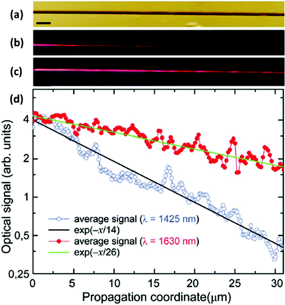 | ||
| Fig. 13 CPP propagation length estimation using NSOM measurements. (a) Topographical optical image of the tapered-groove under test. Scale bar is 2 μm. (b, c) NSOM images of the tapered-groove supporting CPP modes for excitation wavelengths (b) λ = 1425 nm and (c) λ = 1630 nm. (d) Measured optical signal of the CPP modes in (b, c) averaged transverse to the propagation direction; the fitted exponential dependencies of the signal are included. (Adapted with permission from ref. 84 Copyright © 2011 Optical Society of America.) | ||
Following from the above results, a directional coupler consisting of two adjacent, parallel V-groove waveguides (Fig. 14) was demonstrated.106 Here, the proof-of-principle was shown using a separation distance between the waveguides of d = 0.25 μm [Fig. 14(a)–(c)] across telecommunications wavelengths. The error bars in Fig. 14(b) denote the uncertainty related to the CPP mode intensity dependence on the NSOM probe penetration depth inside the groove. The output cross-talk was measured to be close to 0 dB after 40 μm of coupling length, with minimal dependence on wavelength. Numerical calculations performed by finite element method (COMSOL Multiphysics) showed the existence of even [Fig. 14(d)] and odd [Fig. 14(e)] supermodes for the vector field of Ex. Based on the approximately equal power splitting in the measurements, it was understood that the odd mode contributes most to the energy exchange of the coupler, since the even mode with less confinement experiences greater scattering loss from surface roughness. The coupling length, given as Lcoupling = λ/[2(Nodd − Neven)], was found to be around 90 μm, satisfying the basic requirement of Lcoupling ≤ LCPP in this case. The crosstalk was also characterized in this work as a function of light wavelength and d in order to determine the maximum allowed density of non-interacting waveguides, where it was found that no coupling between V-grooves occurred for d = 2 μm and indicating a clear potential for highly miniaturized integration.
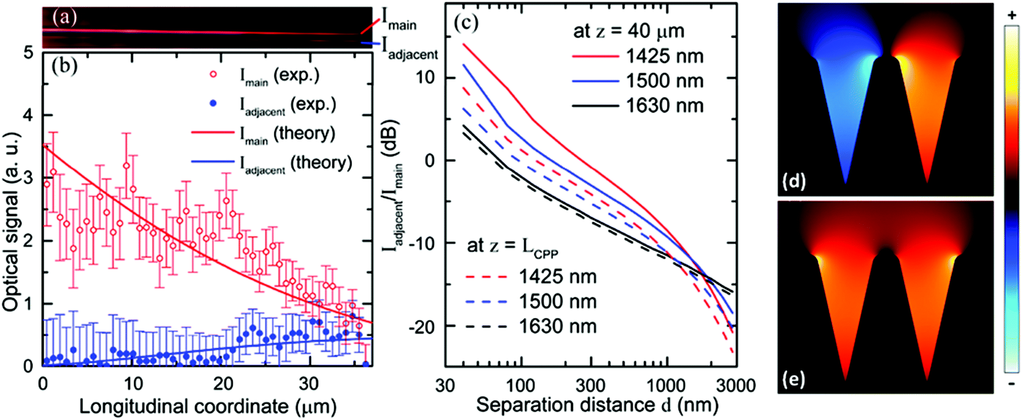 | ||
| Fig. 14 (a) NSOM optical image of the coupling region for a directional coupler with a separation distance of d = 0.25 μm at an excitation wavelength of λ = 1500 nm. Experimental values of the optical signal corresponding to the image of (a) for the main (red hollow circles) and adjacent (blue filled circles) waveguides and compared with the results of numerical simulations. (c) Crosstalk Iadjacent/Imain calculated numerically as a function of separation d varied from 40 nm to 3000 nm at different wavelengths: 1425 nm (red lines), 1500 nm (blue lines), and 1635 nm (black lines) and at different longitudinal coordinates along the coupler region: z = 40 μm (solid lines) and z = LCPP (dashed lines). (d, e) Distribution of the dominant electric field component, Ex, of (d) even and (e) odd supermodes using a light wavelength of λ = 1500 nm calculated with COMSOL. Panel sizes in (d) and (e) are 2.5 μm. (Adapted with permission from ref. 106 Copyright © 2012 Optical Society of America.) | ||
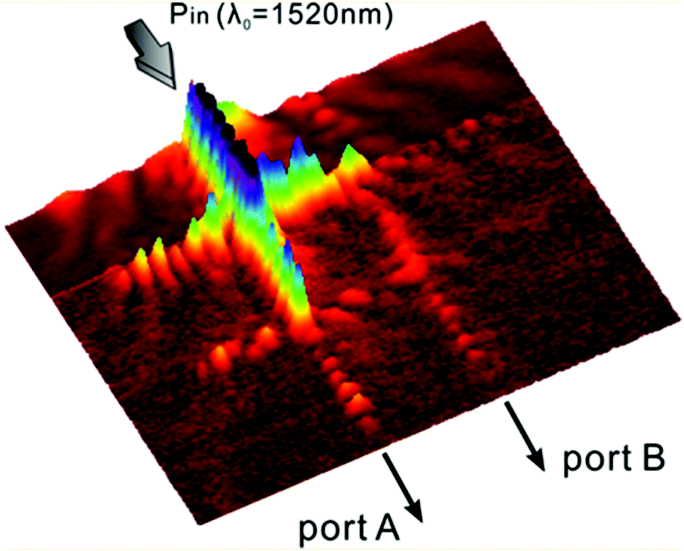
As a testament to their integrability, an implementation of plasmonic V-grooves in a 2 × 2 port logic element based on a resonant guided wave network (RGWN) configuration (Fig. 15) was recently reported.108 The operating principle of the device relied on the ability of two intersecting subwavelength plasmonic waveguides to generate four-way power splitting at their junction; an otherwise cumbersome feat to achieve for dielectric photonic structures. Here, highly confined CPPs supported by the subwavelength plasmonic V-grooves could enter the crossing and undergo volumetric mode expansion, resulting in an isotropic in-plane distribution of k-vectors and thereby coupling to all four ports. Since the power splitting ratios into the outgoing ports were determined by a resonance condition at the intersection, the RGWN could be tailored to route different wavelengths to separate transmission ports. Moreover, it was suggested that four V-groove waveguides as per the arrangement indicated in Fig. 15 potentially enables a facile eight-port device, which cannot be matched by other photonic crystal or plasmonic add/drop filters where only two on/off states are accessible. As such, RGWNs of plasmonic V-grooves represent a manifestly straightforward and effective approach to develop power splitters and logic elements for nanocircuits.
 | ||
| Fig. 15 The measured near-field response of a 2 × 2 port RGWN logic device composed of four 15 μm-long V-groove waveguides. The plasmonic mode of one of the arms is coupled to from a silicon ridge waveguide with TE-polarised light of λ0 = 1520 nm. The output ports are labelled A and B. (Adapted with permission from ref. 108 Copyright © 2014 American Chemical Society.) | ||
In the pursuit of generally improving plasmonic component quality and production affordability, nanoimprint lithography was adopted to form tapered-groove waveguides consisting of Bragg grating filters.89 The wavelength-selective filtering was demonstrated experimentally by NSOM (Fig. 16), and supplemented by in-plane optical transmission measurements. The in-plane measurements were made possible by the nature of the samples being stand-alone: that is, end-facets at both ends of ∼100 μm-length waveguides were accessible by lensed optical fibers due to the fabrication method including a UV lithography step that could define narrow yet robust polymer substrates. The results of the two separate experiments on the same device [16 period, Λ = 760 nm (12.1 μm-length) grating] compared favorably to previous focused ion beam (FIB)-milled periodic wells,90 where NSOM scans along the waveguide direction observed an extinction ratio, Ii/Io, of 4.5 ± 0.9 [Fig. 16(a)] taken before and after the corrugation and within the appropriate wavelength range, while transmission measurements exhibited a maximum extinction ratio of 8.2 dB (center wavelength, λ0 = 1454 nm) and a −3 dB bandwidth of Δλ = 39.9 nm. It is intriguing to note that the reported center wavelengths of the Bragg gratings in both ref. 89 and 90 are several percentage points shorter than the expected values according to the grating pitches and mode effective refractive indices, and remains a topic of interest that possibly involves more complicated physical phenomena. Nevertheless, the high-throughput nanoimprint lithography technique used to fabricate the devices, to be discussed further in section 4, consolidates the prospects of achieving high quality and mass-production-compatible nanoplasmonic components.
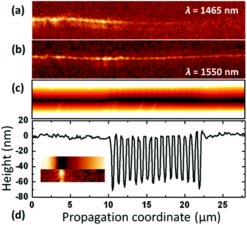 | ||
| Fig. 16 NSOM measurements on a tapered-groove containing a 16-period Bragg grating filter. (a, b) 5.0 × 27.9 μm panels of NSOM measurements taken along the V-groove for the excitation wavelengths of (a) λ = 1465 nm and (b) λ = 1550 nm. (c) Topographical optical image taken by atomic force microscopy for the same region of (a) and (b). (d) Cross-section close to the tapered-groove bottom from (c) with inset: 5 × 1 μm panels showing topography and near-field optical intensity (λ = 1550 nm) taken simultaneously by the NSOM probe. (Adapted with permission from ref. 89 Copyright © 2012 Optical Society of America.) | ||
Alternative tapered-groove geometries have been considered with the aim of combining the advantages of other plasmonic waveguide configurations together with those offered by CPPs. The effects of a finite metal thickness have been numerically investigated,104,105 where short-170 and long-range SPPs171–173 (SR-SPPs and LR-SPPs) were considered in the context of V-grooves for achieving short- and long-range CPPs (SR-CPPs and LR-CPPs). SR-SPPs and LR-SPPs, which are supported by thin metal films surrounded by dielectric media, have the tangential electric field profile (main damping component) either efficiently occupying the metal with large confinement and Ohmic dissipation (SR-SPPs), or exhibiting a central null inside the metal with minimal confinement and Ohmic dissipation (LR-SPPs). SR-CPPs were shown to exhibit a strong dependence on the metal film thickness, with a decreasing thickness resulting in progressively increased confinement and losses.104 This behavior, in accordance with expected SR-SPP characteristics, suggests a useful method to tailor the CPP mode properties where the metal thickness is the variable parameter. Along similar lines, LR-CPPs of a gold film sandwiched between symmetric dielectric media (n1 = n2 = 2.38) were explored105 where the mode distribution [Fig. 17(a)] was found to be notably larger than the CPP counterpart, indicating longer propagation lengths – order of millimeters for telecommunications wavelengths – at the cost of reduced integration density. The strict requirement for symmetry of the surrounding dielectric media for LR-CPP modes suggests other possibilities, where the high sensitivity to small refractive index changes may be useful to LOC sensing devices.
 | ||
| Fig. 17 (a) Normalized dominant electric field profile, Ex, of a LR-CPP supported by a 10 nm gold film sandwiched between symmetric dielectric media with θ = 30°, a groove depth of 5 μm and an excitation wavelength of λ = 1550 nm.105 (b) Electric field distribution of the fundamental hybrid-plasmonic waveguide mode with a SiO2 gap thickness of t = 20 nm between a Si wedge and an Ag tapered-groove at an excitation wavelength of λ = 1550 nm.107 (Adapted with permission from ref. 105 and 107 Copyright © 2011 Optical Society of America, © 2013 IOP Publishing Ltd.) | ||
Another alternate tapered-groove geometry somewhat resembling the hybrid-plasmonic configuration68,135 was suggested and numerically investigated.107 A V-groove of silver (εm = −129 + 3.3i), predominantly filled with silicon (εd = 12.25), had a silicon dioxide (SiO2) (εg,c = 2.25) gap layer located between the Si and Ag [λ = 1550 nm, Fig. 17(b)]. It was shown that the mode energy of the hybrid plasmon-polariton could be strongly confined to the low-index dielectric gap region while maintaining reasonable propagation lengths on the order of tens of microns. A performance comparison between hybrid V-grooves and standard V-grooves in air suggested that modes supported by hybrid geometries can exhibit superior properties in terms of a combined effective mode area reduction and propagation length. Practical aspects of the scheme, such as fabrication and characterization, warrant further investigation, but make for clear paths to future work since the scheme potentially offers the advantage of seamlessly integrating tapered plasmonic grooves with Si-based photonics and electronics.
3.2 Quantum plasmonics
Arguably the most rapidly emerging field of research in nanophotonics is the topic of quantum plasmonics, which studies the quantum nature of light and its interaction with matter on the nanoscale. The ability of plasmonic systems to concentrate EM fields beyond the diffraction limit make for new possibilities to achieve quantum-controlled devices, such as single-photon sources, qubit operators and transistors.22–25 As we will discuss in the following, recent work has shown numerically that tapered plasmonic grooves can efficiently collect and enhance the emission from a local quantum emitter109–113 as well as facilitate the entanglement between separated qubits,110–112 making the tapered-groove a well-suited structure type to incorporate into future quantum plasmonic systems.A particular advantage of tapered plasmonic grooves with respect to emitter-waveguide systems is their combination of subwavelength confinement and one-dimensional character, which was proposed as a means to mediate the resonant energy transfer between quantum emitters.110 For such systems, a major parameter is the coupling efficiency, β, defined as the ratio of spontaneous emission coupled into the plasmonic waveguide mode, ![[small gamma, Greek, circumflex]](https://www.rsc.org/images/entities/i_char_e0b2.gif) plas, to the sum of decay rates into all available paths, tot; i.e. β = plas/tot. The plasmonic V-groove stands out as a competitive structure in terms of promoting a large maximum β due to the strong EM confinement it offers. In addition, the CPP mode profile supports a broad range of emitter heights within the structure, h, where β remains high [Fig. 18(a)]. The influence of groove angle and tip radius on an emitter–groove system has been quantified,113 where β was found to be large [Fig. 18(b) and (c)] within a small window of parameters. Owing to existing limits on fabrication precision at the nanoscale and the importance of maximizing β in quantum-optics systems, the sensitivity of emitter–groove coupling on geometrical parameters therefore demands a detailed knowledge of these settings in order to predict the possible range of βs available. Nevertheless, the results above110,113 highlight the fact that tapered grooves offer a robust scheme to realize strong emitter–waveguide coupling across a broad range of readily-achievable specifications.
plas, to the sum of decay rates into all available paths, tot; i.e. β = plas/tot. The plasmonic V-groove stands out as a competitive structure in terms of promoting a large maximum β due to the strong EM confinement it offers. In addition, the CPP mode profile supports a broad range of emitter heights within the structure, h, where β remains high [Fig. 18(a)]. The influence of groove angle and tip radius on an emitter–groove system has been quantified,113 where β was found to be large [Fig. 18(b) and (c)] within a small window of parameters. Owing to existing limits on fabrication precision at the nanoscale and the importance of maximizing β in quantum-optics systems, the sensitivity of emitter–groove coupling on geometrical parameters therefore demands a detailed knowledge of these settings in order to predict the possible range of βs available. Nevertheless, the results above110,113 highlight the fact that tapered grooves offer a robust scheme to realize strong emitter–waveguide coupling across a broad range of readily-achievable specifications.
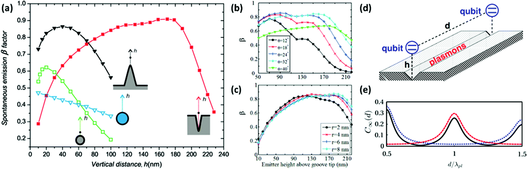 | ||
| Fig. 18 (a) Spontaneous emission β-factor of a single emitter in the neighborhood of various silver plasmonic waveguides as a function of the emitter height, h, at the excitation wavelength of λ = 600 nm.110 (b, c) Coupling efficiency of an emitter into the plasmonic mode of a gold V-groove at an excitation wavelength of λ = 632.8 nm as a function of vertical emitter height in the groove. Different groove angles, θ, are considered in(b) for a groove depth of d = 120 nm, while in (c) different tip radii are considered for a groove depth of d = 150 nm at a fixed groove angle, θ = 26°.113 (d) Schematic illustration of two qubits interacting via a plasmonic V-groove waveguide.112 (e) Steady-state concurrence as a function of separation between two equal qubits with β = 0.94 and propagation length LCPP = 2 μm for a silver V-groove (θ = 20°, 140 nm groove depth) at an excitation wavelength of around λ = 640 nm under three different laser configurations on the two qubits (see text): asymmetric (solid black curve), symmetric (dotted blue line), and antisymmetric (dashed red line).112 (Adapted with permission from ref. 110, 113 and 112] Copyright © 2010 American Chemical Society, © 2012 American Institute of Physics,© 2011 American Physical Society.) | ||
As a next step towards the realization of quantum-operating devices, a numerical study of the entanglement between two emitters mediated by a V-groove waveguide was reported [Fig. 18(d)].111,112 The steady-state entanglement driven by continuous laser pumping was described,112 where large values of the concurrence (measure of entanglement)174 were shown to be achievable for qubit–qubit distances larger than the operating wavelength. In particular, the steady-state concurrence, C∞, was investigated as a function of qubit separation, d/λpl (λpl the wavelength of the plasmon), under continuous laser pumping on the two qubits [Fig. 18(e)]. Three configurations of the laser-driven Rabi frequencies on the two qubits, Ω1 and Ω2, were studied: (1) symmetric with Ω1 = Ω2 = 0.1γ for preparing the |+〉 state (γ denotes the decay rate); (2) antisymmetric with Ω1 = −1Ω2 = 0.1γ for preparing the |−〉 state; and (3) asymmetric with Ω1 = 0.15γ and Ω2 = 0 for preparing a mixture of |+〉 and |−〉 states resulting in a changed separation dependence on C∞. It was further elucidated that the two-qubit entanglement generation is essentially due to the Ohmic dissipation part of the effective qubit–qubit coupling caused by the mediating plasmons.111 The significance of this points to the concept of implementing dissipative engineering of states to achieve quantum-operating devices111,112 where the plasmonic V-groove represents a realistic structure to facilitate sufficient entanglement between the separated qubits.
The V-groove waveguide in a ring resonator configuration [Fig. 19(a) and (b)] was reported with the aim to achieve strong control over the spontaneous emission of a local emitter.109 According to Fermi's golden rule, the rate of spontaneous emission of an optical emitter is proportional to the local density of states (LDOS), which may be increased in an optical micro-cavity by the Purcell factor,175
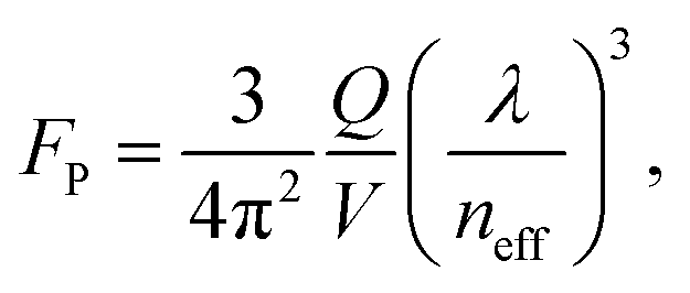 | (3.1) |
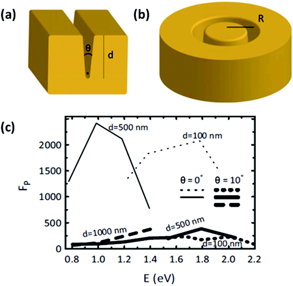 | ||
| Fig. 19 (a, b) V-groove-based ring resonator geometry. The solid dot in (a) indicates the position at which the LDOS was calculated. (c) Purcell factors of fundamental CPP modes with m = 1 azimuthal cavity resonance for different V-groove parameters as a function of energy. The lower three curves are for resonators with θ = 10°, where FP can be more than 350. For the resonators based on thin grooves (θ = 0°), FP reaches over 2000. (Adapted with permission from ref. 109 Copyright © 2010 American Institute of Physics.) | ||
We note here that tapered grooves are especially interesting structures in the context of quantum plasmonics, since their demonstrations as effective nanophotonic circuit elements make them ideal to serve as connectors to and from miniaturized quantum systems. Furthermore, tapered grooves represent a straightforward geometry to fill with and align the relevant quantum emitter materials, pointing to a relative ease of device formation. However, experimental demonstrations of quantum devices consisting of tapered plasmonic grooves are yet to be reported in the literature, thus setting the stage for exciting developments to come in the pursuit of general and groove-based quantum plasmonics.
3.3 Advanced light absorbers and filters
Periodic arrays of grooves, implemented to make practical use of plasmonic nanofocusing in tapered structures, were recently shown to be able to modify metal surfaces from having a highly reflective character (shiny) into exhibiting efficient, broadband absorption (dark).86,93,114,115 Early blackened metal surfaces, produced by distillation at high pressures177 or intense laser irradiation,178,179 were able to suppress reflection through a combined effect of nano-, micro- and macro-structured surface morphology, however, such surfaces are essentially impossible to design, characterize and reproduce down to all fine details due to the high degree of randomness. Alternatively, approaches utilizing resonant interference have achieved efficient absorption properties for metal surfaces via structures such as gratings and micro-cavities, but inevitably come with wavelength, angular or polarization dependencies, thereby reducing their effectiveness e.g. for photovoltaic and thermophotovoltaic applications. In order to overcome the limitations inherent to random- and resonant-based metal light absorbers, so-called “black gold” surfaces were realized by broadband nonresonant adiabatic nanofocusing of GSPs excited by scattering off from the subwavelength-sized wedges of ultra-sharp convex groove arrays86,93,114–116 (phenomena described in section 2). While other determinable and nonresonant light absorption configurations had been demonstrated at the time, such as subwavelength cylinders150 and spheres,151 these configurations only supported limited absorption efficiencies due to their small absorption cross-sections relative to the geometry. By contrast, convex grooves may be fabricated to occupy large fractions of the surface area [Fig. 20(a) and (d)], thereby resulting in an efficient scheme to achieve broadband light absorption.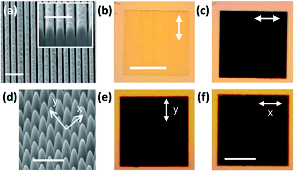 | ||
| Fig. 20 (a) Scanning electron micrograph of a 1D array of ultra-sharp convex grooves in gold (scale bar is 1 μm). (b, c) Optical micrographs of the device from (a) illuminated with light polarized along the grooves (b), and across the grooves (c), demonstrating the polarization dependence on light absorption here (scale bar is 1 μm). (d) Scanning electron micrograph of a 2D array of ultra-sharp convex grooves in gold (scale bar is 700 nm). (e, f) Optical micrographs of the device from (d) illuminated with orthogonal polarizations, demonstrating the reduced polarization dependence on the light absorption for the 2D case (scale bar is 7 μm). (Adapted with permission from ref. 93 Copyright © 2012 Macmillan Publishers Ltd.) | ||
The first proof-of-concept of plasmonic black gold by adiabatic nanofocusing reported an average reflectivity of 4.0% was reported across the wavelength range 450–850 nm.93 The influence of period dimension (1D or 2D arrays of grooves) was reported, where the 1D case exhibited a polarization dependence based on whether the incident electric field corresponded to the dominant component of the GSPs (perpendicular to the groove axis) [Fig. 20(b) and (c)]. It was shown that the polarization dependence could be otherwise mitigated by implementing 2D arrays of grooves, which facilitated the efficient excitation of GSPs for polarizations oriented along both groove axes [Fig. 20(e) and (f)].93,116 Conversely, the polarization dependence of the 1D case was exploited for the design of broadband linear polarizers operating in reflection, where a factor of 3.9 suppression for p-polarized light relative to s-polarized light was experimentally achieved.86 These devices were additionally shown to induce negligible spectral broadening of ultra-short (5–10 fs) laser pulses, leading to a new class of high-damage-threshold, low-dispersion polarizing filters. These demonstrations highlight a key practical advantage of plasmonic black gold: its tailorable reflective properties, which can be selected to suit particular applications.
Methods to further enhance the light absorption in plasmonic groove arrays have been investigated.114–116,121 The use of other metals with larger plasmonic losses was initially proposed93 and later validated using nickel114 and palladium.116 The potential advantages of using other metals includes lower production costs, higher melting temperatures (∼1550 °C in the case of palladium),116 and the possibility to allow for more practical fabrication techniques such as nanoimprint lithography or reactive-ion etching. A report on the spectral response showed a generally increasing reflectivity to occur for longer wavelengths, but with a remarkable dip that could be tuned by precise groove geometries – a feature potentially useful for selective thermal emitters in thermophotovoltaics.114 The influence on reflectivity for a wide range of parameters, including groove profile, groove depth, bottom groove width, period, width of flat plateau, choice of metal and general direction of light incidence, have also been quantified.115,121 In particular, the importance of realizing the adiabatic condition was highlighted, with nearly parallel groove walls at the groove bottom being required in all cases to sufficiently suppress reflection. However, away from the groove bottom, broader taper angles were found to be otherwise permissible since the adiabatic condition could be met more easily, thereby enabling a large fraction of the surface to collect incident light for achieving efficient absorption.115 Calculations for angles of light incidence along the plane containing the groove axis generally showed lower reflectance across the wavelength spectrum than for angles along the plane normal to the groove axis,121 suggesting that this direction would be preferable for applications pertaining to thermophotovoltaics, concentrated solar power or broadband polarizers where low reflectivity is sought and different angles of incidence might occur. Moreover, we note here that the presence of antisymmetric GSPs caused by slight asymmetries in the groove profiles may also play an important role in the design of further-improved light absorbing metals, since these modes are optically dark (propagation lengths below 10 nm) and could therefore provide an extremely efficient channel to dissipate the incident light.85
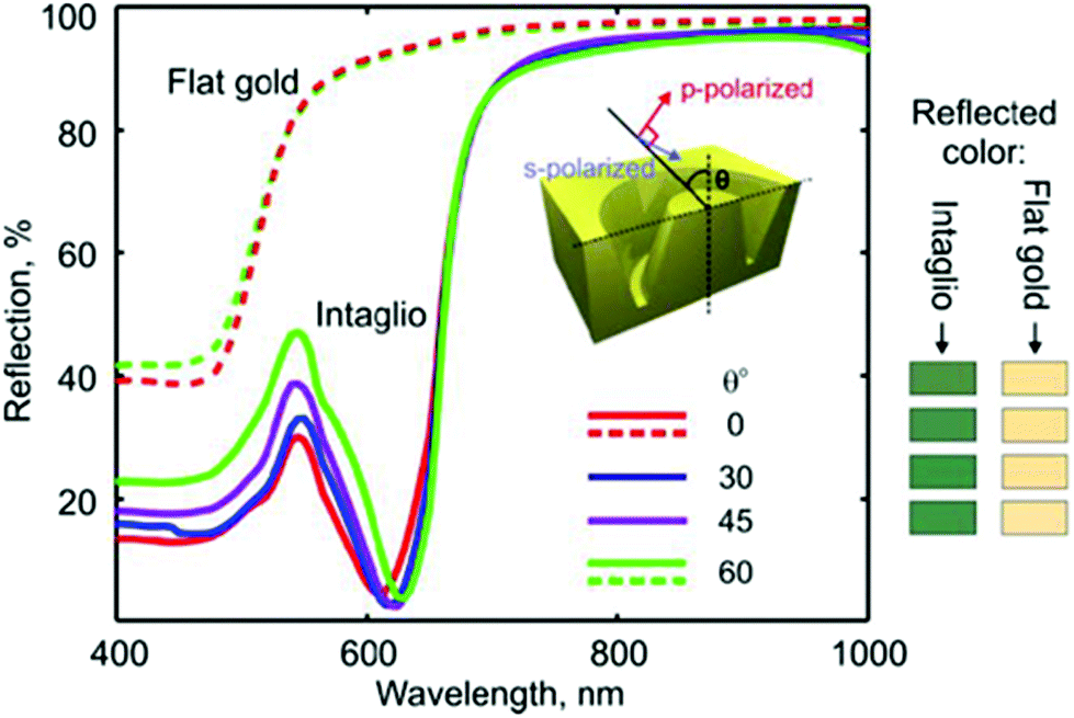
Plasmonic relief meta-surfaces were experimentally shown to control the perceived color of light reflected from metals.118,119 The configuration consisted of periodic, tapered-groove-based ring resonators that were engineered to absorb select wavelength components of the visible spectrum and thereby change the spectra reflecting back from the surface (Fig. 22).118 The functionality of the design relied on a combination of the resonant properties of the plasmonic rings together with a sub-wavelength periodicity of the array which excluded diffraction effects and rendered the scheme viewing-angle-invariant. The platform, suitable to nanoimprint-based fabrication techniques since the structuring was of continuous metal (no perforations), points towards an affordable approach to realize structurally-based, high-resolution colored surfaces that do not require pigments or other chemical modification.
In contrast with the above configurations that consider reflection, the case of transmission through gold films perforated with holes of tapered gap widths [Fig. 21(a)] was shown to further boost extraordinary optical transmission (EOT).87,95,117 EOT describes the resonantly-enhanced transmission of light through periodically spaced, subwavelength apertures in otherwise opaque metallic films,26–28 which was enhanced here by the use of large entrance apertures that collected the incident light and adiabatically funneled it as GSPs through the taper to exit smaller apertures. The maximum transmission at resonance was found to occur for taper angles in the range of 6°–10°,117 supporting a significant increase in transmission compared to straight slits. For a 180 nm gold film on glass, an enhanced EOT with resonance transmission as high as ∼0.18 for a filling ratio of ∼g/Λ = 0.13 was experimentally achieved with clear theoretical agreement [Fig. 21(b)].95 Following this, a numerical study into the effect of higher diffraction and slit resonance orders caused by an increased metal film thickness showed that the maximum transmission occurred when only the fundamental reflection order and at the same time higher transmission orders were available, implying that an optimum metal film thickness exists even though thicker metals would allow for larger collection apertures;117 a 250 nm gold film in air was shown to potentially yield a factor of more than 20 times higher transmission relative to the gap-to-period ratio. Accordingly, the use of tapered slits points to numerous approaches for augmenting the range of applications that EOT phenomena are suited for, including subwavelength optics, optoelectronics, chemical sensing and biophysics.27
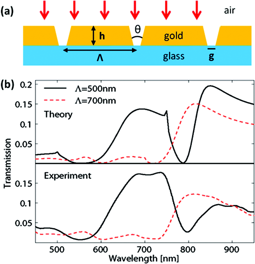 | ||
| Fig. 21 (a) Illustration of a periodic array of tapered slits in a gold film of thickness h, period Λ, taper angle θ and gap at the bottom, g. The gold film resides on a glass substrate. (b) Theoretically calculated and experimentally measured zero-order transmission spectra from normally incident light for a structure with g = 65 nm, θ = 20.5° and periods Λ = 500 and 700 nm. The resonant transmission is as high as ∼0.18 for a filling ratio of ∼g/Λ = 0.13. (Adapted with permission from ref. 95 Copyright © 2010 American Chemical Society.) | ||
 | ||
| Fig. 22 Tapered-groove-based photonic metamaterial for engineering the spectral response of metals in the visible region. The graph depicts the color invariance with viewing angle: numerically simulated spectra and associated perceived colors for an array of tapered-groove-rings in gold with 170 nm diameters and a depth of 180 nm viewed at normal incidence and a selection of oblique angles (as labeled, averaged over incident s- and p-polarizations). For comparison, the corresponding perceived color of an unstructured gold surface is shown for each viewing angle, and reflection spectra for the unstructured metal at 0° and 60° angles are plotted. (Reprinted with permission from ref. 118 Copyright © 2011 Optical Society of America.) | ||
3.4 Novel lab-on-a-chip systems
Plasmonics is playing an increasing role in LOC devices since the EM field enhancement it offers has led to significant improvements in detection capabilities,31–36 imaging resolutions37,39–41,180 and nano-manipulation control.42–46 The over-arching advantage of plasmonic components in this respect lies with their ability to achieve highly concentrated EM fields while remaining within the technologically mature and non-obtrusive nature of the optical domain. The prospect of utilizing tapered plasmonic grooves in particular for LOC devices in the pursuit of point-like, on-chip light sources and biosensors was initially demonstrated with the report that fluorescent beads within the groove contour could be individually excited by CPPs.181 Importantly, the tapered-groove profile was shown in this work to provide topography-assisted self-alignment of particles of interest, a unique and highly appropriate feature for LOC devices that acts in addition to the benefit offered by supporting SPPs.Several different LOC-suitable approaches for achieving radiation nanofocusing in tapered plasmonic grooves have been reported in the literature. Appreciable field concentration (∼λ/40) in V-shaped grooves was demonstrated by collecting normally incident radiation and compressing it as GSPs into nanoscale gaps located at the groove tips.182 Also under normal illumination, resonant field enhancement of reflected GSPs in periodic arrays of tapered grooves, caused by a deliberate break down of the adiabatic condition, was shown to exhibit enhancement factors up to 550148 theoretically and ∼110 experimentally (see Fig. 23).87,94 Alternatively, V-grooves tapered along the waveguiding axis as discussed in section 2 have demonstrated adiabatic nanofocusing of channeled plasmons,60,67,161 where the field enhancement factors reached up to ∼1200 theoretically60,67,161 and ∼130 experimentally.60,161 In light of these reports, it is evident that tapered plasmonic grooves not only offer strong field enhancement suitable for LOC devices, but also a broad choice of design options due to the variety of configurations that can achieve it.
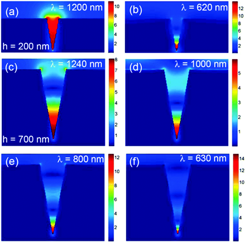 | ||
| Fig. 23 Calculated normalized field magnitude distributions at resonant wavelengths as indicated on images for two 20° angle grooves with depths h = (a, b) 200 nm and (c, e, f) 700 nm. The distributions show the resonant GSP standing-wave patterns of different orders, m = (a) 1, (b, c) 2, (e) 3 and (f) 4. For comparison, a nonresonant field distribution is shown in (d) for h = 700 nm. (Reprinted with permission from ref. 94 Copyright © 2010 American Chemical Society.) | ||
A nano-opto-mechanical device platform consisting of a plasmonic V-groove was theoretically considered as an approach to mediate the auto-oscillatory motion of individual nano-objects via normally incident light (Fig. 24).122 The configuration was such that for specific conditions of particle polarizability and V-shaped profile, an electric field distribution forms inside the groove as a result of the control beam (250 mW μm−2) and exerts an upwards force on a nano-object at the bottom of the groove – sufficient to overcome gravity and van der Waals attraction by an order of magnitude. The vertical component of the optical gradient force varies strongly as a function of the particle's position, with its direction reversing beyond a certain equilibrium point in the groove and hence facilitating auto-oscillatory motion. Importantly, the intensity of the control beam governs the magnitude of the up and down accelerations and therefore the particle's round-trip frequency, which, depending on particle and groove specifications, may be varied to achieve a range of 22–40 MHz. The configuration could be of interest to the development of low energy all-optical information technologies that do not require nonlinear materials, or LOCs that employ motion-based transduction or operate by means of optical actuation.
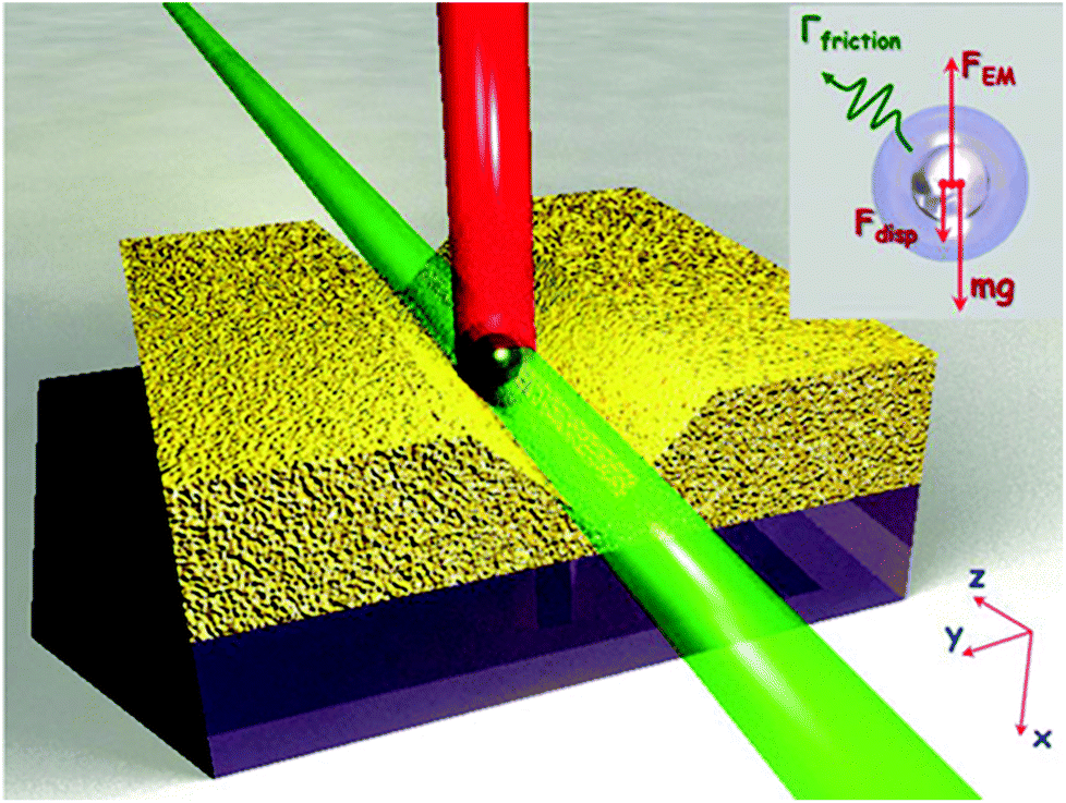 | ||
| Fig. 24 Schematic of the nano-opto-mechanical modulator: a nanoparticle in the V-groove waveguide is driven into auto-oscillatory motion by a control beam (red). The particle moves in and out of the fundamental mode of the waveguide (green) and modulates modal loss. Inset shows the forces acting on a nano-object inside the V-groove. (Reprinted with permission from ref. 122 Copyright © 2013 John Wiley and Sons.) | ||
The use of divergent tapered nanogrooves was recently suggested as a method to improve the resolution of conventional light microscopes.120 Owing to the eminent role of light microscopy in science and its establishment as a routine investigative tool, the possibility to break the optical diffraction barrier without fluorescent labels is tantalizing to researchers since a wide variety of fundamental building blocks in the life and physical sciences are of nanoscale dimensions. The scheme (Fig. 25) suggests subwavelength features may be collected in real-time with the nanogroove magnifier and remitted as an image to be captured by traditional lenses; calculations indicate a potential resolution of ∼λ/32 = 25 nm for 40 nm-wide waveguides. In another arrangement that also associates the use of tapered grooves with optical microscopes, termination mirrors at the ends of tapered-groove waveguides have been shown to provide a highly convenient approach to efficiently excite in-plane CPPs via direct illumination from microscope objectives.88,92 The importance of this result, which we will discuss further in section 5, corresponds to enabling new opportunities for sensing and manipulation via LOC devices in microscope settings where the photon-to-plasmon efficiency would otherwise act as a limiting factor. In sum, we anticipate tapered plasmonic grooves to play an increasing role in optical microscopes and microscope-based LOC devices.
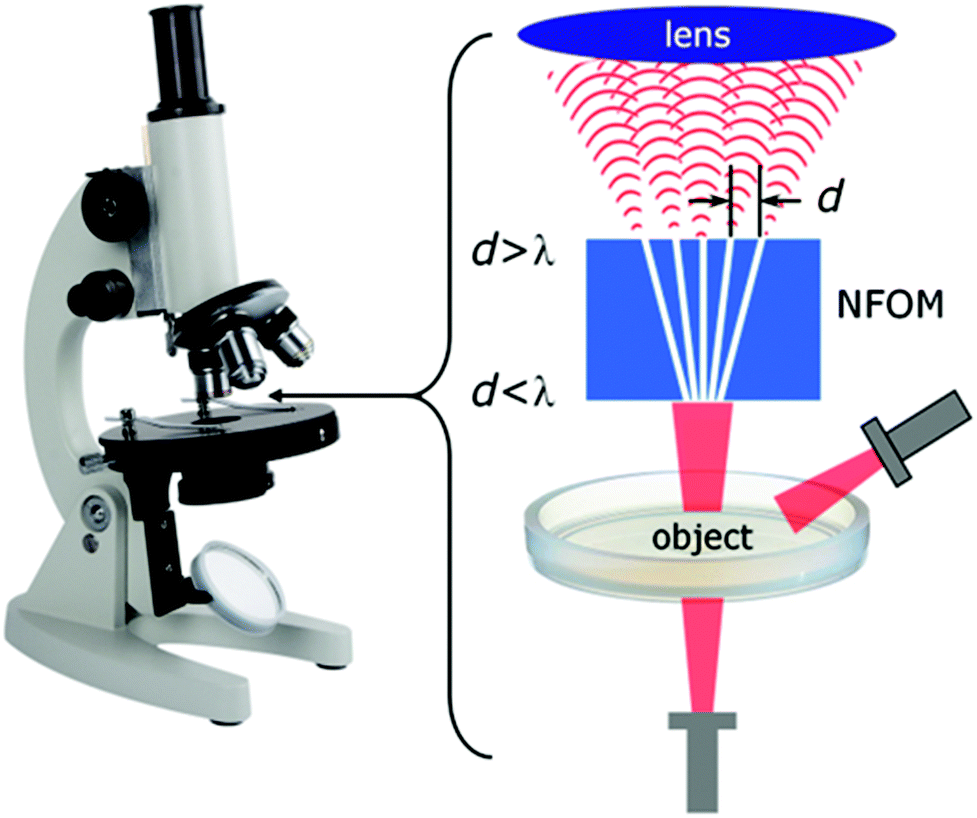 | ||
| Fig. 25 Schematic of imaging with proposed near field optical magnifier comprised of nanowaveguides (white lines) supported by dielectric filler (blue). The subwavelength-size “object” is placed at the input ends of the nanowaveguides array (having waveguide separation d < λ). When illuminated, the image of the object is propagated along the waveguides and re-emitted as a magnified image at the output ends of the waveguides (with separation d > λ). Traditional optics are used to capture the magnified image. (Reprinted with permission from ref. 120 Copyright © 2014 Optical Society of America.) | ||
4 Fabrication
The increasing prevalence of nanofabrication techniques has led to the rapid growth of the field of plasmonics over the past fifteen years.48–51 The strong dependence on feature-size for nanofocusing light via plasmons implies that the ability to routinely pattern metals on the nanoscale allows for the advantages of SPPs to be systematically harnessed. Nevertheless, fabrication challenges still remain in terms of achieving high quality and cost-effective nanoplasmonic devices suitable for technological integration (e.g. CMOS compatibility). In this light, tapered grooves represent comparatively convenient planar plasmonic structures to fabricate since they correspond to the innate profiles formed by focused-ion beam (FIB) milling or crystallographic etching of silicon. In the following, we present the variety of lithographic techniques that have been demonstrated to form metallic tapered-groove profiles and discuss their relative merits.4.1 Focused-ion beam milling
Today, the most common procedure for fabricating tapered plasmonic grooves is via the use of FIB milling, where a finely focused beam of (typically gallium) ions sputters material away from a specific location. Owing to the broad flexibility it offers for generating arbitrary metal geometries with feature sizes below 10 nm, FIB milling represents the “go-to” approach for fast prototyping – tapered grooves included.12,93,97,108,118,182 In addition to the broad selection of structure types that can be realized by FIB milling, modern FIB systems are also commonly available at research facilities and processing centers, making it a relatively accessible technique.Despite the diverse set of tapered plasmonic grooves that have been achieved via FIB milling, issues related to either its production rate or quality must be borne in mind. Concerning the production rate, FIB milling is a serial-based technique, which leads to long writing times per device that render it impractical for large-scale fabrication. In terms of production quality, the act of sputtering material away from a region inherently leads to its re-deposition nearby, a problem that results in the deterioration of side-wall smoothness97 and causes damage to already-formed structures in close proximity.93 Furthermore, some gallium ions become implanted into the top few nanometers of the metal surface, causing non-negligible effects into the behavior of the free electrons.183 Recent demonstrations of helium-based FIB milling make for a viable alternative to gallium sources in terms of producing high quality devices with minimal structural and material degradation.184 Helium-based FIB milling therefore represents a compelling avenue to improve upon existing demonstrations and promote new opportunities, although its serial-based aspect still retains the high labor-intensive- and time-related costs inherent to FIB processes.
4.2 Anisotropic etching
V-shaped grooves produced by anisotropic (crystallographic) etching have been shown to support CPPs with propagation lengths exceeding 100 μm for excitation wavelengths around λ = 1.5 μm.91 Anisotropic etching involves the use of a wet chemical agent that etches crystalline materials at considerably different rates depending on which crystal face is exposed. In the case of 〈100〉-oriented silicon with potassium hydroxide (KOH) as the etchant, the 〈111〉 set of silicon crystal planes etch at a much slower rate than all others (e.g. ∼400 times slower than 〈100〉). As a consequence, V-shaped grooves with a fixed groove angle of θ = 70.6°, corresponding to the crossing of 〈111〉 silicon crystal planes, can be defined using an etch mask of SiO2.91,123,182 A major advantage of anisotropic etching is its suitability for wafer-scale production, since the etching agent can act over one or more whole wafers simultaneously. Additionally, the groove-formation using this method relies on a chemical process that results in almost atomically-smooth sidewalls and tips with curvature radii sharper than 5 nm.88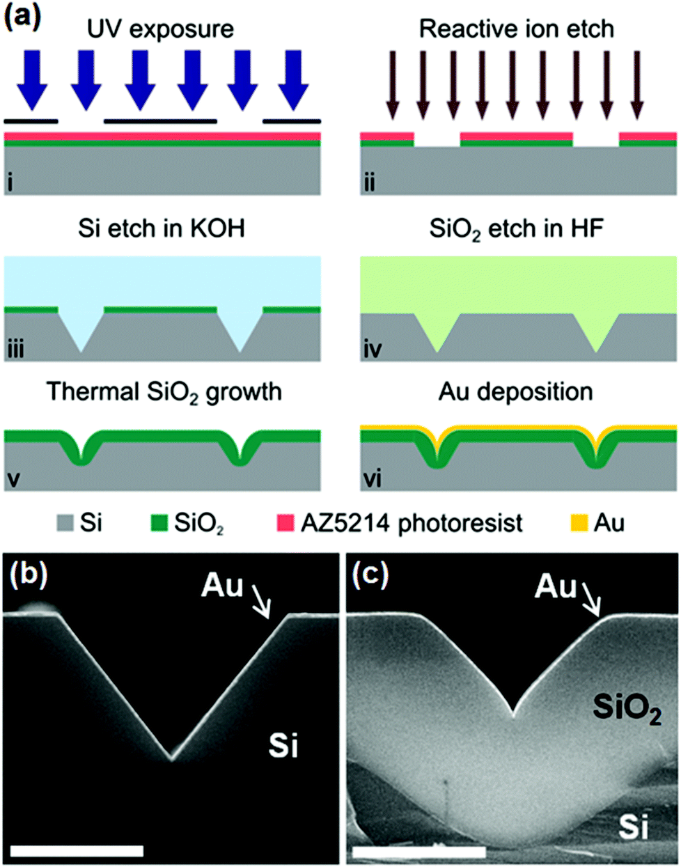 | ||
| Fig. 26 (a)[i–vi] The procedure for fabricating gold V-grooves by photolithography combined with anisotropic etching in KOH. The SiO2 etch mask is removed by hydrofluoric acid (HF). A thermal oxidation step may be performed to modify the V-groove profile before the gold layer is deposited. (b, c) SEM images of resulting V-groove cross-sections: (b) without thermal oxidation, and (c) with thermal oxidation. Scale bars are 2 μm. (Adapted with permission from ref. 88 Copyright © 2014 American Chemical Society.) | ||
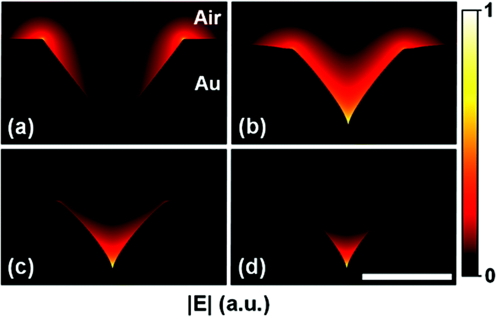 | ||
| Fig. 27 FEM calculations of the magnitude of the electric fields supported by varying V-groove cross-sections in gold for an excitation wavelength of λ = 811 nm. (a) Zero oxidation. In this case, only modes located at the wedges exist; (b) 1320 nm oxidation; (c) 1720 nm oxidation; and (d) 2320 nm oxidation. Thicker SiO2 layers lead to sharper V-shaped profiles near the tip resulting in increased confinement of the electric field distribution towards the bottom of the waveguide. A clear CPP mode occurs in the case for (d). Scale bar is 2 μm. (Adapted with permission from ref. 88 Copyright © 2014 American Chemical Society.) | ||
Alternatively, we posit that a method to etch higher-index crystal planes in silicon at slower rates than the 〈111〉 set would potentially allow for the formation of sharper grooves with smaller θ. For example, the crossing of certain planes of 〈311〉 with respect to 〈100〉 would result in θ = 34.8°. Additives including isopropyl alcohol (IPA) or Triton-x-100 surfactant to etchants such as KOH or tetramethylammonium hydroxide (TMAH) have been shown to change the preferred, slowest-etch-rate crystal plane.185 Standards to select higher index planes are not well-established to the best of our knowledge, but we remark that such an approach could be ideal to make tailored, reproducible V-grooves without additional process steps.
Importantly, the combined procedure here is able to maintain the cost advantages of wafer-scale production while simultaneously yielding high quality plasmonic devices. In addition, propagation-length measurements on such devices have been consistent with curvature radii below 5 nm despite the rounding effects that could be expected from metallization,88 indicating that the approach offers a facile method to realize nanometer-scale features. Furthermore, since the photolithography step is only required to define relatively large feature sizes (>100's nanometers), equipment specifications are relaxed and widely accessible.
4.3 Nanoimprint lithography
Nanoimprint lithography (NIL) represents an exceptionally low-cost, high-throughput fabrication method that may be used to manufacture plasmonic devices.51,187 It essentially involves the creation of a hard, reusable, nanostructured master stamp that is pressed into relatively soft polymer material. Importantly, the NIL process is highly repeatable, which leads to production expenses that are scarcely more than the energy and material costs involved. NIL relies on mechanical deformation to transfer the pattern from stamp to the polymer, a physical process that enables structure dimensions to be defined well beyond the limitations of light diffraction or beam scattering; demonstrations of NIL routinely achieve ∼10 nm features188 and 1–2 nm189 has been reached. Furthermore, NIL-based techniques offer new paths to improve structured-metal surface roughness through the use of atomically-smooth stamps and thermal relaxation, and can employ diverse mold types such as metal direct nanoimprinting (embossing) for the fabrication of plasmonic components and other metal-containing optical (and electronic) devices.190,191The ability to mass-produce plasmonic components via NIL is of significant consequence and potentially renders a host of plasmonics-based applications economically viable. The implications for integrated optics alone are tremendous, with NIL representing the only established method to form complex plasmonic components on a wafer scale. In addition, large surface-area technologies such as black metals, structurally-colored surfaces and enhanced light filters, as well as disposable devices such as sensitive diagnostic tools, threat detectors and environmental monitors are all poised to benefit from the high-throughput production offered by NIL.
Plasmonic V-grooves have been fabricated by NIL91,123 using a double pattern transfer method that replicated the structures of a stamp into metal. The technique relied on the greater adhesion of titanium to Ormocomp than the gold to poly(methylmethacrylate) (PMMA), thereby allowing for the double pattern transfer. This fabrication process was an extension of previous results that produced sharp metal wedges via controlled profiling of a silicon stamp followed by a single pattern transfer.192 The double-transfer NIL method for making V-grooves has been further built upon with the introduction of Bragg gratings added to the V-grooves of the stamp by electron-beam lithography; the NIL process is illustrated in Fig. 28(a) and the SEM image of one such V-groove consisting of Bragg gratings shown in Fig. 28(b).89
 | ||
| Fig. 28 (a)[i–iv] The NIL fabrication scheme for producing gold V-grooves. [i] A silicon stamp containing of the V-grooves (and optional Bragg gratings) is imprinted into PMMA polymer resist, resulting in an inverted polymer replica of the stamp. [ii] Gold (200 nm) is deposited on the patterned polymer followed by a (5 nm) titanium adhesion-promoting layer. [iii] Ormocomp is cast over the metal and defined by UV-lithography to form device-specific polymer substrates. [iv] Ion-beam-etching with the Ormocomp layer as an etch-mask removes the unwanted metal. The PMMA layer is then dissolved in acetone, releasing the stand-alone plasmonic components. (b) SEM of a gold V-groove produced by NIL consisting of a Bragg grating. The scale bar is 1 μm. (Adapted with permission from ref. 89 Copyright © 2012 Optical Society of America.) | ||
5 Excitation and characterization
A variety of configurations have been developed to excite and characterize SPPs based on either photonic or electronic approaches. In both cases, the conversion efficiency represents a major topic to overcome due to otherwise inherent mismatch involved in the photon–plasmon or electron–plasmon couplings. Furthermore, the characterization of the generated plasmons must account for the non-radiative and potentially nanoscale aspect they possess. Despite these challenges, recent reports using tapered grooves cite significant progress regarding high photon–plasmon coupling efficiencies,88,116 and super-resolved characterization of GSP modes has been demonstrated.85 In this section, we review the methods that have been established to excite and characterize plasmons in tapered grooves, focusing on recent achievements and the opportunities they present.5.1 Photon–plasmon techniques
Methods to promote efficient photon–plasmon coupling generally fall under one of two categories: overcoming the wavevector (momentum) mismatch,6,126 or maximizing the field amplitude overlap integral.193 Wavevector matching may be achieved by prism- or resonant-based couplers, which under specific configurations can supply the additional momentum necessary for photons to match plasmons (and vice versa). While prism-based approaches may be regarded as bulky or limited to many plasmonic systems due to the requirement of additional high refractive index materials, resonant-based schemes have been shown to offer both compactness and high coupling efficiency, with prominent examples including Yagi–Uda antennas,194 phase-engineered elements195 and grating couplers.196 For tapered-groove based devices, resonant coupling is partly responsible for the photon–plasmon conversion in enhanced transmission filters.95 Despite the success of resonant-based couplers to plasmonics, maximizing the field overlap is the prevailing technique for exciting plasmons in tapered grooves due to its practical simplicity and effectiveness. This holds true even for most resonator-type configurations of tapered grooves, since the plasmon excitation is still initiated by the field overlap at the interface between the source and plasmonic mode.94,95,118 As a result, the most common configurations to facilitate photon–plasmon exchange in tapered grooves are end–fire coupling and direct illumination, both of which can promote large, or at least sufficient, field overlap integrals.Despite the prevalence of end–fire coupling, one should be mindful of two important drawbacks that are especially the case for tapered grooves. First, the requirement of a cleaved sample end-facet, for which the cleaving process itself is cumbersome, deteriorates the waveguide entrance quality and leaves it prone to further damage. Second, the coupling efficiency is critically and uniquely sensitive to fiber position and orientation, which causes routine measurements on similar devices to be challenging and imprecise. These drawbacks, while often acceptable, have nevertheless spurred investigation into other field-overlap-based techniques.
There are two established mechanisms to excite plasmonic modes in tapered grooves using the field overlap from direct illumination. First, the plasmon excitation can be initiated by scattering of the incident light off from the outer edges of the grooves (wedges), where the coupling efficiency is determined by the mode match at the interface. This scattering mechanism is responsible for light-SPP coupling in the cases of plasmonic black metals,93 coloured and field-enhanced surfaces,94,118 and boosted EOT filters.95 Larger groove openings generally correspond to larger field overlap integrals and therefore promote higher photon–plasmon conversion ratios, with plasmonic black metal designs achieving efficiencies at least as high as 97%.116
The second mechanism involves the use of nanomirrors (Fig. 29), where normally incident light is redirected along the direction of propagating CPPs and the resulting field overlap with the plasmonic mode facilitates the photon–plasmon coupling.88,92 The dependence of the incident electric field orientation on the coupling efficiency has been shown to allow for confirmation of the photon–plasmon coupling via nanomirrors [Fig. 29(d) and (e)] due to the strongly polarised nature of the supported plasmonic modes. The most efficient nanomirror inclination angle has been found to be 45°,92 corresponding to the maximum redirection of light into the propagation axis. Initial demonstrations of FIB-milled nanomirrors provided maximum coupling efficiencies up to 10%,92 with more recent devices fabricated by photolithography and anisotropic etching indicating >50% photon–plasmon coupling due to an increased light collection area of the mirror and smoother metal surfaces.88 Nanomirror designs that further optimize this collection area, together with the use of inclination angles at or close to 45°, could expect to realize even higher photon–plasmon coupling efficiencies.
 | ||
| Fig. 29 (a) Setup for direct illumination of CPPs via nanomirrors. Light from a laser diode is linearly polarized before impinging onto the sample through a microscope objective. (b) Bright-field image of a V-groove device with waveguide termination nanomirrors. The scale bar is 4 μm. (c)–(e) Experimentally observed radiation from the out-coupling termination mirrors at the ends of the waveguides. The larger spots on the left are the direct reflection from the incident beam and the right spots (green arrows) are out-coupled light from the termination mirrors. Insets at the bottom left of the images represent the polarization of the incident electric field. (c) A pair of intensity peaks corresponding to the wedge-based pair of modes occurs for the case without oxidation. (d) A single intensity peak corresponding to a CPP mode is out-coupled from a V-groove device with a 2320 nm SiO2 layer. The incident polarization closely matches the electric field of the CPP and leads to efficient in-coupling. (e) A reduced out-coupled intensity occurs for the same device in (d) when the incident light polarization is rotated 90° and no longer matches the CPP electric field. (Adapted with permission from ref. 88 Copyright © 2014 American Chemical Society.) | ||
Recently, integrated waveguide coupling was implemented for exciting plasmonic modes in tapered grooves via the photonic modes of silicon ridge waveguides (Fig. 30).108 The source light (telecommunications wavelengths) was initially coupled into the silicon waveguide by means of a grating coupler that could select either the transverse electric (TE) (electric field parallel to the substrate) or the transverse magnetic (TM) photonic modes (electric field perpendicular to the substrate) depending on the angle of excitation. Due to the strongly polarized nature of the plasmons supported in tapered grooves (section 2), the choice of TE or TM modes in the silicon waveguide subsequently determined whether groove-based CPP modes or wedge-based SPP modes were launched at the ridge-groove interface. By means of this selective capability, the coupling to highly confined CPP modes could be confirmed and therefore enabled significant progress to be made towards the realization of advanced integrated silicon/plasmonic nanocircuits. The scheme's initial coupling efficiency into the CPP mode, calculated to be ∼22.2%,108 was well sufficient for demonstration purposes and may be improved upon by further optimization of the field overlap integral.
 | ||
| Fig. 30 Schematic of the configuration for coupling to V-groove plasmonic modes from a silicon ridge waveguide. (Adapted with permission from ref. 108 Copyright © 2014 American Chemical Society.) | ||
The NSOM technique has been used extensively to directly map the properties of CPPs in plasmonic V-grooves, including propagation length,84,97 subwavelength mode confinement84,161 and mode effective refractive indices,84 as well as the operation of novel components.12,89,90,108 However, accurate NSOM measurements require deep knowledge of the interaction between the near-field probe and the sample under test;199 in the case of tapered grooves, it is crucial to account for the spatial convolution caused by the near-field probe profile and the V-shaped geometry (Fig. 31).84 Furthermore, inherent problems related to instabilities of the probe-surface distance have proven to be difficult to avoid, especially in narrow and deep V-grooves, which can complicate precise CPP characterization.84 Nevertheless, NSOM measurements have provided a wealth of information of plasmons in tapered grooves, and, due to their expediency, can provide immediate explicit insight that would otherwise only be indirectly available through time-consuming full field simulations.
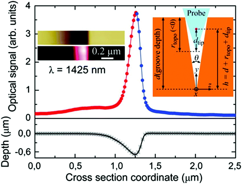 | ||
| Fig. 31 Transverse profile of a propagating CPP mode (filled circles) and the V-groove topography (asterisks) as taken by an NSOM probe. Left insets: images corresponding to the near-field and topographical scans. Right inset: cross-section schematic of the V-groove/NSOM probe configuration under consideration. The probe cannot reach the bottom of the groove. (Adapted with permission from ref. 84 Copyright © 2011 Optical Society of America.) | ||
5.2 Electron–plasmon techniques
The excitation of plasmons by electrons is a potentially enabling approach to integrate electronics with photonics200,201 that additionally offers the possibility to retrieve unprecedented spatial information of the optical modes in a plasmonic device.85,202,203 A range of electron–plasmon techniques are available that may be categorized based on whether the acceleration voltage of the electron source is low (<10 V) or high (100's kV). Low-voltage-source electrons, e.g. delivered by scanning tunneling microscopes,200,201 are appropriate for the exploration of effective electronic–photonic integration schemes since the associated configurations could be feasibly miniaturized and are not demanding in terms of power consumption. A low-voltage scheme for exciting plasmons in tapered grooves by electrons is yet to be demonstrated, but would represent an important advance towards their technological development. High-voltage-source electrons, e.g. fired in a tightly focused beam at a metal surface,204 have been used to map plasmonic modes with sub-nanometer spatial resolution and allow for investigations into the properties of extremely confined plasmons that are otherwise inaccessible.85 In the following, we discuss the results of such a high-voltage electron–plasmon technique, from which extremely confined GSP modes in tapered grooves have been studied.EELS-based investigations have enabled the unique opportunity to probe GSP modes in the crevice of nanogrooves with structural feature sizes below 5 nm.85 The first use of electron-based techniques to excite propagating plasmons occurred in the 1970s to measure the dispersion of SPPs on thin aluminum films,211 yet aside from otherwise preliminary investigations of GSPs in MIM structures (10 nm dielectric gaps) with cathodoluminescence,212 the first nanoscale exploration of GSP modes using electrons happened only very recently.85 The cause of this 40-year delay resided mainly in the difficulty to prepare an appropriate (e.g. ∼150 nm-thick) cross-sectional slice of the plasmonic device suitable for measurements (Fig. 32). Particular cross-section thicknesses are required for EELS in order to render the samples sufficiently transparent for the electron beam to pass through and also reduce the influence of Cherenkov radiation, while not being too thin compared to the propagation length of the GSP modes under investigation. For the recent EELS-based investigation of nanogrooves,85 procuring a ∼150 nm-thick cross-section required a challenging process that involved first protecting the device via SiO2 and platinum deposition, cutting out a section from a larger sample by FIB techniques, welding the section to a lift-out grid, and further refining the lamella thickness carefully by additional FIB profiling.85 While we note that only very lossy modes with propagation lengths on the order of a few tens of nanometers [i.e. the antisymmetric GSP mode (section 6)] could be investigated here85 as a result of the lamella's thinness (albeit offering significant insights), we foresee in the near future that EELS may be employed to precisely investigate modes of longer propagation length by considering other protective dielectric materials or configurations and thicker lamellas (several 100's of nanometers). Furthermore, we anticipate the use of EELS-based methods to study the presence of non-local effects (section 6) where the maximum possible confinement of plasmonic modes is limited by quantum-wave phenomena.
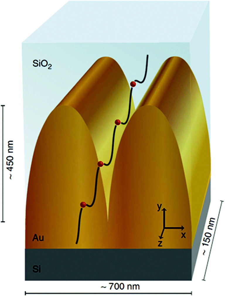 | ||
| Fig. 32 Artistic impression of a gold nanogroove with a swift electron beam moving parallel to the groove axis. The groove is filled with SiO2 and the substrate is silicon. (Reprinted with permission from ref. 85 Copyright © 2014 Macmillan Publishers Ltd.) | ||
6 Challenges
In this section we discuss several challenges critical to the design of tapered-groove-based devices. In general, our relatively newfound ability to control light on the nanoscale has led us to interact with otherwise unnoticed effects, such as the non-local response or unintended device asymmetries, both of which can profoundly influence system behaviour. Here we focus on the challenges such effects present to the implementation of tapered grooves, and follow with a discussion of the issues that remain for integrating tapered grooves into practical device platforms. We remark that the general and otherwise important topic of circumventing plasmonic losses127,128,130,213 is beyond the scope of this review, which as of this writing remains unexplored for tapered grooves.6.1 Non-local effects
In our considerations so far, we have discussed the properties of plasmons in the context of classical electrodynamics and the Drude local-response approximation (LRA) of the polarization, where the current density is locally related to the electrical field through Ohm's law.126 However, extreme subwavelength mode confinement draws attention to non-local effects beyond the local Drude description due to the quantum-wave nature of the electron gas at the nanoscale.214,215 In noble-metal systems, the relevance of non-local corrections to the LRA picture can be estimated from the non-local length scale , where β ∝ vF is the speed of longitudinal pressure waves in the plasma and D is a constant for charge-carrier diffusion that accounts phenomenologically for e.g. surface scattering and Landau damping.216 Typically, the non-local lengthscale is in the sub-nanometer regime.214
Tapered groove structures have been used as an initial model system217 to appreciate the enormous surface-enhanced Raman scattering (SERS) effect on metal surfaces with nanoscale roughness.218 Studies in this regard have since illustrated the need for going beyond the LRA,219 where the intrinsic length scale δnl of the electron gas has been shown to smear out otherwise-assumed field singularities.124 As a consequence, the SERS enhancement factor remains finite (Fig. 33) even for geometries with infinitely sharp features. The qualitative aspects of non-locality seem to have been experimentally confirmed in a configuration of graphene on the rough silver surfaces of tapered grooves,220 where the SERS enhancement was more accurately predicted by accounting for non-local effects. Numerical studies have shown that the properties of waveguides may also be affected by non-local responses, with tapered-groove waveguides exhibiting a fundamental limit on the achievable mode confinement.125 This translates into a maximum ceiling on the Purcell enhancement of dipole-emitter decay systems that could be reached, and may have important implications in quantum plasmonics (section 3).
 | ||
| Fig. 33 Schematic of the system used for studying non-local effects in tapered grooves. (a) Array of grooves formed by half-cylindrical nanorods. (b) Cross-section of the unit cell. (c) and (d) Typical electric-field intensity and charge distributions for a dipole mode. (Reprinted with permission from ref. 124 Copyright © 2012 Optical Society of America.) | ||
6.2 Antisymmetric GSPs
GSP modes may be classified according to the symmetry of the electric field component oriented across the MIM gap, which can be either symmetric – i.e. those discussed so far in this Review – or antisymmetric. Unlike symmetric GSPs, antisymmetric GSPs (aGSPs) feature very strong absorption (propagation lengths of order 10 nm)85 due to their symmetric induced-charge patterns. Such a rapid decay of energy implies that any coupling contributions into aGSP modes may be regarded as loss, yet this also makes useful investigations into their occurrence a non-trivial task.Recently, the presence of aGSPs in tapered grooves was confirmed experimentally using high spatial and energy resolution EELS.85 The technique involved scanning the electron probe from the top towards the bottom of a thin convex groove lamella while monitoring the EELS response (Fig. 34). The blue-shift of the resonance peak indicated the onset of an aGSP mode in the narrowing crevice of the groove (down to ∼5 nm width) rather than the exclusive presence of (global) groove GSP modes whose peak positions would otherwise not depend on the electron location in the groove.
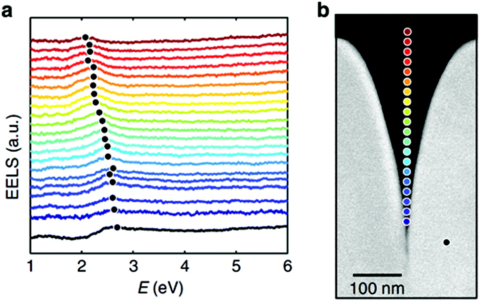 | ||
| Fig. 34 (a) Waterfall plot of experimental EELS measurements at the corresponding positions indicated on the groove image in (b). (Reprinted with permission from ref. 85 Copyright © 2014 Macmillan Publishers Ltd.) | ||
While the EELS technique generated aGSP modes by symmetric charge depletion in the groove from the electron probe, an important insight of photon–plasmon coupling into aGSP modes was obtained in the study regarding the supporting structure's asymmetry. For example, black gold based on convex groove arrays showed experimentally greater-than-expected light absorption,93 since they were initially simulated by perfectly symmetric features and normally incident light such that the absorption was thought to be based solely on the dissipation of symmetric GSP modes. For the symmetric case, incident plane waves generate charged dipole moments that may be conceptually decomposed into two SPPs forming at each wedge in antiphase propagating downwards into the groove. However, the configurations in practice consisted of slight structural asymmetries and inclined light, which in turn allowed for the SPPs excited at opposite wedges to meet in the interior of the groove with relative antiphase-shifts and thereby contribute energy into lossy aGSP modes. It should be noted that ideal-case symmetrical systems – i.e. the condition considered in most numerical simulations – do not support the generation of aGSP modes by light, leaving their influence on real devices otherwise unnoticed. Accordingly, the presence of aGSPs represents an easily-overlooked yet potentially crucial factor to consider when practically implementing nanoplasmonic devices that could be affected by additional channels of energy dissipation, e.g. in black metals,116 quantum emitter systems,110 or logic circuits with junctions/bends.108
6.3 Integration
Plasmonic systems require methods to interface with the external world that are not only favorable in terms of fabrication (section 4) and coupling efficiency (section 5), but are also able to simultaneously maintain the advantages uniquely offered by the nature of plasmons, such as circuit miniaturization, high information bandwidth and large field enhancement. Integrating devices so as to address this ensemble of requirements represents a major pursuit towards the realization of useful plasmonics-based technologies. In the following, we discuss our thoughts on several specific issues that are important to the integration of tapered plasmonic grooves.7 Outlook
Research into plasmons of tapered grooves has achieved many important milestones to-date that have been central to the development of an assortment of applications and scientific investigations. Progress continues across an increasingly diverse number of fronts that currently includes nanophotonic circuits, quantum plasmonics, light harvesters, high-definition colored surfaces, advanced optical filters, LOC components, and the fundamental understanding of plasmon excitations and their interactions. The motives and successes behind these advances are largely owed to both the unique and common properties that GSPs and CPPs can possess across a variety of configurations and groove profiles. In particular, tapered grooves offer the principle advantages enabled by the nature of plasmons – light confinement beyond the diffraction limit – together with the flexibility of device design and fabrication-method-selection that is unmatched in the field of plasmonics.The first demonstration of plasmonic modes supported by tapered grooves was reported 10 years ago,97 yet the extensive list of results presented throughout our Review suggests that the topic area still remains in its “golden age”. We further remark that there are numerous research directions of potentially major consequence that are yet to be explored. Fully-functioning nanoscale light sources integrated with tapered grooves would open many doors regarding information-based and LOC-type technologies. Turning plasmonic losses around so as to efficiently convert electromagnetic energy into heat inside the grooves could open up new possibilities for realizing thermally-based optical switches or nano-object control. The plasmonic modes located at the outer wedges rather than the groove tips possess relatively large propagation lengths and unique polarization properties that may also facilitate novel device schemes. In any case, the many promising applications offered by plasmonic tapered grooves and the unique possibilities they enable for investigating fundamental light-matter interactions point to exciting research years ahead.
Acknowledgements
C.L.C.S. acknowledges financial support from the Danish Council for Independent Research (grant no. 12-126601). N.S. acknowledges financial support from the Lundbeck Foundation (grant no. R95-A10663). A.K. acknowledges partial financial support from the Innovation Fund Denmark (grant no. 10-092322, PolyNano). N.A.M. acknowledges funding from the Danish Council for Independent Research, (grant no. 1323-00087). S.I.B. acknowledges financial support from the European Research Council (grant no. 341054, PLAQNAP). The Center for Nanostructured Graphene is sponsored by the Danish National Research Foundation (grant no. DNRF58).References
- S. A. Maier, M. L. Brongersma, P. G. Kik, S. Meltzer, A. A. G. Requicha and H. A. Atwater, Adv. Mater., 2001, 13, 1501–1505 CrossRef CAS.
- R. Zia, J. A. Schuller, A. Chandran and M. L. Brongersma, Mater. Today, 2006, 9, 20–27 CrossRef CAS.
- S. Lal, S. Link and N. J. Halas, Nat. Photonics, 2007, 1, 641–648 CrossRef CAS PubMed.
- J. A. Schuller, E. S. Barnard, W. Cai, Y. C. Jun, J. S. White and M. L. Brongersma, Nat. Mater., 2010, 9, 193–204 CrossRef CAS PubMed.
- Z. Han and S. I. Bozhevolnyi, Rep. Prog. Phys., 2013, 76, 016402 CrossRef PubMed.
- H. Raether, Surface plasmons on smooth and rough surfaces and on gratings, Springer, Berlin, 1988 Search PubMed.
- J. Takahara, S. Yamagishi, H. Taki, A. Morimoto and T. Kobayashi, Opt. Lett., 1997, 22, 475–477 CrossRef CAS.
- K. V. Nerkararyan, Phys. Lett. A, 1997, 237, 103–105 CrossRef CAS.
- W. L. Barnes, A. Dereux and T. W. Ebbesen, Nature, 2003, 424, 824–830 CrossRef CAS PubMed.
- D. K. Gramotnev and S. I. Bozhevolnyi, Nat. Photonics, 2010, 4, 83–91 CrossRef CAS PubMed.
- D. K. Gramotnev and S. I. Bozhevolnyi, Nat. Photonics, 2013, 8, 13–22 CrossRef PubMed.
- S. I. Bozhevolnyi, V. S. Volkov, E. Devaux, J.-Y. Laluet and T. W. Ebbesen, Nature, 2006, 440, 508–511 CrossRef CAS PubMed.
- L. Chen, J. Shakya and M. Lipson, Opt. Lett., 2006, 31, 2133–2135 CrossRef CAS.
- A. L. Pyayt, B. Wiley, Y. Xia, A. Chen and L. Dalton, Nat. Nanotechnol., 2008, 3, 660–665 CrossRef CAS PubMed.
- S. Papaioannou, K. Vyrsokinos, O. Tsilipakos, A. Pitilakis, K. Hassan, J. Weeber, L. Markey, A. Dereux, S. I. Bozhevolnyi, A. Miliou, E. E. Kriezis and N. Pleros, J. Lightwave Technol., 2011, 29, 3185–3195 CrossRef.
- M. Kauranen and A. V. Zayats, Nat. Photonics, 2012, 6, 737–748 CrossRef CAS PubMed.
- D. Bergman and M. Stockman, Phys. Rev. Lett., 2003, 90, 027402 CrossRef.
- M. T. Hill, Y.-S. Oei, B. Smalbrugge, Y. Zhu, T. de Vries, P. J. van Veldhoven, F. W. M. van Otten, T. J. Eijkemans, J. P. Turkiewicz, H. de Waardt, E. J. Geluk, S.-H. Kwon, Y.-H. Lee, R. Nötzel and M. K. Smit, Nat. Photonics, 2007, 1, 589–594 CrossRef CAS PubMed.
- R. F. Oulton, V. J. Sorger, T. Zentgraf, R.-M. Ma, C. Gladden, L. Dai, G. Bartal and X. Zhang, Nature, 2009, 461, 629–632 CrossRef CAS PubMed.
- M. A. Noginov, G. Zhu, A. M. Belgrave, R. Bakker, V. M. Shalaev, E. E. Narimanov, S. Stout, E. Herz, T. Suteewong and U. Wiesner, Nature, 2009, 460, 1110–1112 CrossRef CAS PubMed.
- M. Khajavikhan, A. Simic, M. Katz, J. H. Lee, B. Slutsky, A. Mizrahi, V. Lomakin and Y. Fainman, Nature, 2012, 482, 204–207 CrossRef CAS PubMed.
- E. Altewischer, M. P. van Exter and J. P. Woerdman, Nature, 2002, 418, 304–306 CrossRef CAS PubMed.
- A. V. Akimov, A. Mukherjee, C. L. Yu, D. E. Chang, A. S. Zibrov, P. R. Hemmer, H. Park and M. D. Lukin, Nature, 2007, 450, 402–406 CrossRef CAS PubMed.
- S. Kumar, A. Huck and U. L. Andersen, Nano Lett., 2013, 13, 1221–1225 CrossRef CAS PubMed.
- M. S. Tame, K. R. McEnery, S. K. Özdemir, J. Lee, S. A. Maier and M. S. Kim, Nat. Phys., 2013, 9, 329–340 CrossRef CAS PubMed.
- T. W. Ebbesen, H. J. Lezec, H. F. Ghaemi, T. Thio and P. A. Wolff, Nature, 1998, 391, 667–669 CrossRef CAS.
- C. Genet and T. W. Ebbesen, Nature, 2007, 445, 39–46 CrossRef CAS PubMed.
- E. Laux, C. Genet, T. Skauli and T. W. Ebbesen, Nat. Photonics, 2008, 2, 161–164 CrossRef CAS PubMed.
- A. S. Roberts, A. Pors, O. Albrektsen and S. I. Bozhevolnyi, Nano Lett., 2014, 14, 783–787 CrossRef CAS PubMed.
- J. S. Clausen, E. Højlund-Nielsen, A. B. Christiansen, S. Yazdi, M. Grajower, H. Taha, U. Levy, A. Kristensen and N. A. Mortensen, Nano Lett., 2014, 14, 4499–4504 CrossRef CAS PubMed.
- K. Kneipp, H. Kneipp, I. Itzkan, R. R. Dasari and M. S. Feld, J. Phys.: Condens. Matter, 2002, 14, 597–624 CrossRef.
- J. N. Anker, W. P. Hall, O. Lyandres, N. C. Shah, J. Zhao and R. P. Van Duyne, Nat. Mater., 2008, 7, 442–453 CrossRef CAS PubMed.
- K. M. Mayer, F. Hao, S. Lee, P. Nordlander and J. H. Hafner, Nanotechnology, 2010, 21, 255503 CrossRef PubMed.
- T. Chung, S.-Y. Lee, E. Y. Song, H. Chun and B. Lee, Sensors, 2011, 11, 10907–10929 CrossRef CAS PubMed.
- J. Feng, V. S. Siu, A. Roelke, V. Mehta, S. Y. Rhieu, G. T. R. Palmore and D. Pacifici, Nano Lett., 2012, 12, 602–609 CrossRef CAS PubMed.
- P. Zijlstra, P. M. R. Paulo and M. Orrit, Nat. Nanotechnol., 2012, 7, 379–382 CrossRef CAS PubMed.
- N. Fang, H. Lee, C. Sun and X. Zhang, Science, 2005, 308, 534–537 CrossRef CAS PubMed.
- S. W. Hell, Science, 2007, 316, 1153–1158 CrossRef CAS PubMed.
- Y. Xiong, Z. Liu, C. Sun and X. Zhang, Nano Lett., 2007, 7, 3360–3365 CrossRef CAS PubMed.
- N. Liu, M. Hentschel, T. Weiss, A. P. Alivisatos and H. Giessen, Science, 2011, 332, 1407–1410 CrossRef CAS PubMed.
- P. J. Schuck, A. Weber-Bargioni, P. D. Ashby, D. F. Ogletree, A. Schwartzberg and S. Cabrini, Adv. Funct. Mater., 2013, 23, 2539–2553 CrossRef CAS PubMed.
- A. N. Grigorenko, N. W. Roberts, M. R. Dickinson and Y. Zhang, Nat. Photonics, 2008, 2, 365–370 CrossRef CAS PubMed.
- M. L. Juan, M. Righini and R. Quidant, Nat. Photonics, 2011, 5, 349–356 CrossRef CAS PubMed.
- D. Erickson, X. Serey, Y.-F. Chen and S. Mandal, Lab Chip, 2011, 11, 995–1009 RSC.
- Y. Pang and R. Gordon, Nano Lett., 2012, 12, 402–406 CrossRef CAS PubMed.
- O. M. Maragò, P. H. Jones, P. G. Gucciardi, G. Volpe and A. C. Ferrari, Nat. Nanotechnol., 2013, 8, 807–819 CrossRef PubMed.
- G. Baffou and R. Quidant, Laser Photonics Rev., 2013, 7, 171–187 CrossRef CAS PubMed.
- S. A. Maier and H. A. Atwater, J. Appl. Phys., 2005, 98, 011101 CrossRef PubMed.
- W. L. Barnes, J. Opt. A: Pure Appl. Opt., 2006, 8, S87–S93 CrossRef.
- T. W. Ebbesen, C. Genet and S. I. Bozhevolnyi, Phys. Today, 2008, 61(5), 44–50 CrossRef PubMed.
- A. Boltasseva, J. Opt. A: Pure Appl. Opt., 2009, 11, 114001 CrossRef.
- E. Moreno, F. J. García-Vidal, S. G. Rodrigo, L. Martín-Moreno and S. I. Bozhevolnyi, Opt. Lett., 2006, 31, 3447–3449 CrossRef.
- E. N. Economou, Phys. Rev., 1969, 182, 539–554 CrossRef.
- B. Wang and G. P. Wang, Opt. Lett., 2004, 29, 1992–1994 CrossRef.
- G. Veronis and S. Fan, Opt. Lett., 2005, 30, 3359–3361 CrossRef.
- K. Tanaka, M. Tanaka and T. Sugiyama, Opt. Express, 2005, 13, 256–266 CrossRef.
- J. Dionne, L. Sweatlock, H. Atwater and A. Polman, Phys. Rev. B: Condens. Matter, 2006, 73, 035407 CrossRef.
- K. V. Nerkararyan, S. K. Nerkararyan and S. I. Bozhevolnyi, Opt. Lett., 2011, 36, 4311–4313 CrossRef PubMed.
- A. J. Babadjanyan, N. L. Margaryan and K. V. Nerkararyan, J. Appl. Phys., 2000, 87, 3785 CrossRef CAS PubMed.
- V. S. Volkov, S. I. Bozhevolnyi, S. G. Rodrigo, F. J. García-Vidal, T. W. Ebbesen and N. B. Alle, Nano Lett., 2009, 1278–1282 CrossRef CAS PubMed.
- D. K. Gramotnev and M. W. Vogel, Phys. Lett. A, 2011, 375, 3464–3468 CrossRef CAS PubMed.
- B. Desiatov, I. Goykhman and U. Levy, Opt. Express, 2011, 19, 13150–13157 CrossRef CAS PubMed.
- M. Stockman, Phys. Rev. Lett., 2004, 93, 137404 CrossRef.
- D. F. P. Pile and D. K. Gramotnev, Appl. Phys. Lett., 2006, 89, 041111 CrossRef PubMed.
- N. A. Issa and R. Guckenberger, Plasmonics, 2006, 2, 31–37 CrossRef.
- E. Verhagen, M. Spasenović, A. Polman and L. Kuipers, Phys. Rev. Lett., 2009, 102, 203904 CrossRef.
- S. I. Bozhevolnyi and K. V. Nerkararyan, Opt. Lett., 2010, 35, 541–543 CrossRef PubMed.
- R. F. Oulton, V. J. Sorger, D. A. Genov, D. F. P. Pile and X. Zhang, Nat. Photonics, 2008, 2, 496–500 CrossRef CAS PubMed.
- P. West, S. Ishii, G. Naik, N. Emani, V. Shalaev and A. Boltasseva, Laser Photonics Rev., 2010, 4, 795–808 CrossRef CAS PubMed.
- I. Goykhman, B. Desiatov and U. Levy, Appl. Phys. Lett., 2010, 97, 141106 CrossRef PubMed.
- X. Yang, Y. Liu, R. F. Oulton, X. Yin and X. Zhang, Nano Lett., 2011, 11, 321–328 CrossRef CAS PubMed.
- G. V. Naik, V. M. Shalaev and A. Boltasseva, Adv. Mater., 2013, 25, 3264–3294 CrossRef CAS PubMed.
- M. Quinten, A. Leitner, J. R. Krenn and F. R. Aussenegg, Opt. Lett., 1998, 23, 1331–1333 CrossRef CAS.
- S. A. Maier, P. G. Kik, H. A. Atwater, S. Meltzer, E. Harel, B. E. Koel and A. A. G. Requicha, Nat. Mater, 2003, 2, 229–232 CrossRef CAS PubMed.
- T. Xu, Y.-K. Wu, X. Luo and L. J. Guo, Nat. Commun., 2010, 1, 59 Search PubMed.
- J. Henzie, M. H. Lee and T. W. Odom, Nat. Nanotechnol., 2007, 2, 549–554 CrossRef CAS PubMed.
- I. Puscasu and W. L. Schaich, Appl. Phys. Lett., 2008, 92, 233102 CrossRef PubMed.
- S.-W. Qu and Z.-P. Nie, Sci. Rep., 2013, 3, 3172 Search PubMed.
- G. W. Bryant, F. J. García de Abajo and J. Aizpurua, Nano Lett., 2008, 8, 631–636 CrossRef CAS PubMed.
- S. Kawata, Y. Inouye and P. Verma, Nat. Photonics, 2009, 3, 388–394 CrossRef CAS PubMed.
- M. Schnell, A. García-Etxarri, A. J. Huber, K. Crozier, J. Aizpurua and R. Hillenbrand, Nat. Photonics, 2009, 3, 287–291 CrossRef CAS PubMed.
- L. Novotny and N. van Hulst, Nat. Photonics, 2011, 5, 83–90 CrossRef CAS PubMed.
- A. Huck, S. Kumar, A. Shakoor and U. L. Andersen, Phys. Rev. Lett., 2011, 106, 096801 CrossRef.
- V. A. Zenin, V. S. Volkov, Z. Han, S. I. Bozhevolnyi, E. Devaux and T. W. Ebbesen, J. Opt. Soc. Am. B, 2011, 28, 1596–1602 CrossRef CAS.
- S. Raza, N. Stenger, A. Pors, T. Holmgaard, S. Kadkhodazadeh, J. B. Wagner, K. Pedersen, M. Wubs, S. I. Bozhevolnyi and N. A. Mortensen, Nat. Commun., 2014, 5, 4125 CAS.
- E. Skovsen, T. Sondergaard, C. Lemke, T. Holmgaard, T. Leißner, R. L. Eriksen, J. Beermann, M. Bauer, K. Pedersen and S. I. Bozhevolnyi, Appl. Phys. Lett., 2013, 103, 211102 CrossRef PubMed.
- J. Beermann, T. Søndergaard, S. M. Novikov, S. I. Bozhevolnyi, E. Devaux and T. W. Ebbesen, New J. Phys., 2011, 13, 063029 CrossRef.
- C. L. C. Smith, A. H. Thilsted, C. E. Garcia-Ortiz, I. P. Radko, R. Marie, C. Jeppesen, C. Vannahme, S. I. Bozhevolnyi and A. Kristensen, Nano Lett., 2014, 14, 1659–1664 CrossRef CAS PubMed.
- C. L. C. Smith, B. Desiatov, I. Goykmann, I. Fernandez-Cuesta, U. Levy and A. Kristensen, Opt. Express, 2012, 20, 5696–5706 CrossRef PubMed.
- V. S. Volkov, S. I. Bozhevolnyi, E. Devaux, J.-Y. Laluet and T. W. Ebbesen, Nano Lett., 2007, 7, 880–884 CrossRef CAS PubMed.
- R. B. Nielsen, I. Fernandez-Cuesta, A. Boltasseva, V. S. Volkov, S. I. Bozhevolnyi, A. Klukowska and A. Kristensen, Opt. Lett., 2008, 33, 2800–2802 CrossRef.
- I. P. Radko, T. Holmgaard, Z. Han, K. Pedersen and S. I. Bozhevolnyi, Appl. Phys. Lett., 2011, 99, 213109 CrossRef PubMed.
- T. Søndergaard, S. M. Novikov, T. Holmgaard, R. L. Eriksen, J. Beermann, Z. Han, K. Pedersen and S. I. Bozhevolnyi, Nat. Commun., 2012, 3, 969 CrossRef PubMed.
- T. Søndergaard, S. I. Bozhevolnyi, J. Beermann, S. M. Novikov, E. Devaux and T. W. Ebbesen, Nano Lett., 2010, 10, 291–295 CrossRef PubMed.
- T. Søndergaard, S. I. Bozhevolnyi, S. M. Novikov, J. Beermann, E. Devaux and T. W. Ebbesen, Nano Lett., 2010, 10, 3123–3128 CrossRef PubMed.
- D. F. P. Pile and D. K. Gramotnev, Opt. Lett., 2004, 29, 1069–1071 CrossRef CAS.
- S. Bozhevolnyi, V. Volkov, E. Devaux and T. Ebbesen, Phys. Rev. Lett., 2005, 95, 046802 CrossRef.
- S. Bozhevolnyi, V. Volkov, E. Devaux, J.-Y. Laluet and T. Ebbesen, Appl. Phys. A: Mater. Sci. Process., 2007, 89, 225–231 CrossRef CAS PubMed.
- J. Q. Lu and A. A. Maradudin, Phys. Rev. B: Condens. Matter, 1990, 42, 11159–11165 CrossRef.
- I. Novikov and A. Maradudin, Phys. Rev. B: Condens. Matter, 2002, 66, 035403 CrossRef.
- S. I. Bozhevolnyi, Opt. Express, 2006, 14, 9467–9476 CrossRef.
- K. C. Vernon, D. K. Gramotnev and D. F. P. Pile, J. Appl. Phys., 2008, 103, 034304 CrossRef PubMed.
- S. I. Bozhevolnyi and J. Jung, Opt. Express, 2008, 16, 2676–2684 CrossRef.
- J. Dintinger and O. J. F. Martin, Opt. Express, 2009, 17, 2364–2374 CrossRef CAS.
- S. Lee and S. Kim, Opt. Express, 2011, 19, 9836–9847 CrossRef CAS PubMed.
- V. A. Zenin, V. S. Volkov, Z. Han, S. I. Bozhevolnyi, E. Devaux and T. W. Ebbesen, Opt. Express, 2012, 20, 6124–6134 CrossRef PubMed.
- Y. Bian, Z. Zheng, X. Zhao, L. Liu, Y. Su, J. Liu, J. Zhu and T. Zhou, J. Opt., 2013, 15, 055011 CrossRef.
- S. P. Burgos, H. W. Lee, E. Feigenbaum, R. M. Briggs and H. A. Atwater, Nano Lett., 2014, 14, 3284–3292 CrossRef CAS PubMed.
- E. J. R. Vesseur, F. J. García de Abajo and A. Polman, Phys. Rev. B: Condens. Matter, 2010, 82, 165419 CrossRef.
- D. Martín-Cano, L. Martín-Moreno, F. J. García-Vidal and E. Moreno, Nano Lett., 2010, 10, 3129–3134 CrossRef PubMed.
- D. Martín-Cano, A. González-Tudela, L. Martín-Moreno, F. J. García-Vidal, C. Tejedor and E. Moreno, Phys. Rev. B: Condens. Matter, 2011, 84, 235306 CrossRef.
- A. Gonzalez-Tudela, D. Martín-Cano, E. Moreno, L. Martin-Moreno, C. Tejedor and F. J. García-Vidal, Phys. Rev. Lett., 2011, 106, 020501 CrossRef CAS.
- K. C. Vernon, N. Tischler and M. L. Kurth, J. Appl. Phys., 2012, 111, 064323 CrossRef PubMed.
- J. Beermann, R. L. Eriksen, T. Søndergaard, T. Holmgaard, K. Pedersen and S. I. Bozhevolnyi, New J. Phys., 2013, 15, 073007 CrossRef.
- T. Søndergaard and S. I. Bozhevolnyi, New J. Phys., 2013, 15, 013034 CrossRef.
- J. Beermann, R. L. Eriksen, T. Holmgaard, K. Pedersen and S. I. Bozhevolnyi, Sci. Rep., 2014, 4, 6904 CrossRef CAS PubMed.
- T. Søndergaard, S. I. Bozhevolnyi, J. Beermann, S. M. Novikov, E. Devaux and T. W. Ebbesen, J. Opt. Soc. Am. B, 2011, 29, 130–137 CrossRef.
- J. Zhang, J.-Y. Ou, N. Papasimakis, Y. Chen, K. F. Macdonald and N. I. Zheludev, Opt. Express, 2011, 19, 23279–23285 CrossRef CAS PubMed.
- J. Zhang, J.-Y. Ou, K. F. MacDonald and N. I. Zheludev, J. Opt., 2012, 14, 114002 CrossRef.
- A. H. Rose, B. M. Wirth, R. E. Hatem, a. P. R. Ahmed, M. J. Burns, M. J. Naughton and K. Kempa, Opt. Express, 2014, 22, 5228–5233 CrossRef CAS PubMed.
- M. Odgaard, M. G. Laursen and T. Søndergaard, J. Opt. Soc. Am. B, 2014, 31, 1853–1860 CrossRef CAS.
- A. S. Shalin, P. Ginzburg, P. A. Belov, Y. S. Kivshar and A. V. Zayats, Laser Photonics Rev., 2014, 8, 131–136 CrossRef CAS PubMed.
- I. Fernandez-Cuesta, R. B. Nielsen, A. Boltasseva, X. Borrise, F. Perez-Murano and A. Kristensen, J. Vac. Sci. Technol., B, 2007, 25, 2649–2653 CAS.
- G. Toscano, S. Raza, S. Xiao, M. Wubs, A.-P. Jauho, S. I. Bozhevolnyi and N. A. Mortensen, Opt. Lett., 2012, 37, 2538–2540 CrossRef CAS PubMed.
- G. Toscano, S. Raza, W. Yan, C. Jeppesen, S. Xiao, M. Wubs, A.-P. Jauho, S. I. Bozhevolnyi and N. A. Mortensen, Nanophotonics, 2013, 2, 161–166 CrossRef PubMed.
- S. A. Maier, Plasmonics: Fundamentals and Applications, Springer, Berlin, 2007 Search PubMed.
- M. A. Noginov, V. A. Podolskiy, G. Zhu, M. Mayy, M. Bahoura, J. A. Adegoke, B. A. Ritzo and K. Reynolds, Opt. Express, 2008, 16, 1385–1392 CrossRef CAS.
- I. De Leon and P. Berini, Nat. Photonics, 2010, 4, 382–387 CrossRef CAS PubMed.
- J. B. Khurgin and G. Sun, Appl. Phys. Lett., 2011, 99, 211106 CrossRef PubMed.
- J. B. Khurgin and G. Sun, Nat. Photonics, 2014, 8, 468–473 CrossRef CAS PubMed.
- L. R. Hirsch, R. J. Stafford, J. A. Bankson, S. R. Sershen, B. Rivera, R. E. Price, J. D. Hazle, N. J. Halas and J. L. West, Proc. Natl. Acad. Sci. U. S. A., 2003, 100, 13549–13554 CrossRef CAS PubMed.
- J. C. Ndukaife, A. Mishra, U. Guler, A. G. A. Nnanna, S. T. Wereley and A. Boltasseva, ACS Nano, 2014, 8, 9035–9043 CrossRef CAS PubMed.
- S. I. Bozhevolnyi, Plasmonic Nanoguides and Circuits, Pan Stanford, Singapore, 2009 Search PubMed.
- J. M. Pitarke, V. M. Silkin, E. V. Chulkov and P. M. Echenique, Rep. Prog. Phys., 2007, 70, 1–87 CrossRef CAS.
- R. F. Oulton, G. Bartal, D. F. P. Pile and X. Zhang, New J. Phys., 2008, 10, 105018 CrossRef.
- M. I. Stockman, Opt. Express, 2011, 19, 22029–22106 CrossRef PubMed.
- E. D. Palik, Handbook of Optical Constants of Solids, Academic, San Diego, 1985 Search PubMed.
- J. B. Khurgin and G. Sun, Opt. Express, 2012, 20, 28717–28723 CrossRef CAS PubMed.
- J. A. Dionne, H. J. Lezec and H. A. Atwater, Nano Lett., 2006, 6, 1928–1932 CrossRef CAS PubMed.
- D. F. P. Pile and D. K. Gramotnev, Opt. Lett., 2005, 30, 1186–1188 CrossRef CAS.
- R. Zia, M. D. Selker, P. B. Catrysse and M. L. Brongersma, J. Opt. Soc. Am. A, 2004, 21, 2442–2446 CrossRef.
- S. Raza, T. Christensen, M. Wubs, S. I. Bozhevolnyi and N. A. Mortensen, Phys. Rev. B: Condens. Matter, 2013, 88, 115401 CrossRef.
- S. I. Bozhevolnyi and K. V. Nerkararyan, Opt. Express, 2009, 17, 10327–10334 CrossRef CAS.
- S. I. Bozhevolnyi, K. V. Nerkararyan and S. B. Hovsepyan, J. Contemp. Phys., 2010, 45, 302–306 CrossRef.
- D. K. Gramotnev, J. Appl. Phys., 2005, 98, 104302 CrossRef PubMed.
- D. Gramotnev and K. Vernon, Appl. Phys. B, 2007, 86, 7–17 CrossRef CAS PubMed.
- K. C. Vernon, D. K. Gramotnev and D. F. P. Pile, J. Appl. Phys., 2007, 101, 104312 CrossRef PubMed.
- T. Søndergaard and S. Bozhevolnyi, Phys. Rev. B: Condens. Matter, 2009, 80, 195407 CrossRef.
- S. I. Bozhevolnyi and K. V. Nerkararyan, Opt. Lett., 2009, 34, 2039–2041 CrossRef.
- A. Aubry, D. Y. Lei, A. I. Fernández-Domínguez, Y. Sonnefraud, S. A. Maier and J. B. Pendry, Nano Lett., 2010, 10, 2574–2579 CrossRef CAS PubMed.
- A. I. Fernández-Domínguez, S. A. Maier and J. B. Pendry, Phys. Rev. Lett., 2010, 105, 266807 CrossRef.
- G. B. Hocker and W. K. Burns, Appl. Opt., 1977, 16, 113–118 CrossRef CAS PubMed.
- A. Polemi, A. Alù and N. Engheta, IEEE Antennas Wireless Propag. Lett., 2011, 10, 199–202 CrossRef.
- D. K. Gramotnev and D. F. P. Pile, Appl. Phys. Lett., 2004, 85, 6323 CrossRef CAS PubMed.
- M. Yan and M. Qiu, J. Opt. Soc. Am. B, 2007, 24, 2333 CrossRef CAS.
- D. F. P. Pile, T. Ogawa, D. K. Gramotnev, T. Okamoto, M. Haraguchi, M. Fukui and S. Matsuo, Appl. Phys. Lett., 2005, 87, 061106 CrossRef PubMed.
- E. Moreno, S. Rodrigo, S. Bozhevolnyi, L. Martín-Moreno and F. García-Vidal, Phys. Rev. Lett., 2008, 100, 023901 CrossRef.
- A. Boltasseva, V. S. Volkov, R. B. Nielsen, E. Moreno, S. G. Rodrigo and S. I. Bozhevolnyi, Opt. Express, 2008, 16, 5252–5260 CrossRef.
- Y. Bian, Z. Zheng, Y. Liu, J. Liu, J. Zhu and T. Zhou, Opt. Express, 2011, 19, 22417–22422 CrossRef CAS PubMed.
- T. Srivastava and A. Kumar, J. Appl. Phys., 2009, 106, 043104 CrossRef PubMed.
- V. S. Volkov, J. Gosciniak, S. I. Bozhevolnyi, S. G. Rodrigo, L. Martín-Moreno, F. J. García-Vidal, E. Devaux and T. W. Ebbesen, New J. Phys., 2009, 11, 113043 CrossRef.
- F. De Angelis, G. Das, P. Candeloro, M. Patrini, M. Galli, A. Bek, M. Lazzarino, I. Maksymov, C. Liberale, L. C. Andreani and E. Di Fabrizio, Nat. Nanotechnol., 2010, 5, 67–72 CrossRef CAS PubMed.
- E. Ozbay, Science, 2006, 311, 189–193 CrossRef CAS PubMed.
- H. A. Atwater, Sci. Am., 2007, 296, 56–63 CrossRef CAS.
- M. J. Dicken, L. A. Sweatlock, D. Pacifici, H. J. Lezec, K. Bhattacharya and H. A. Atwater, Nano Lett., 2008, 8, 4048–4052 CrossRef CAS PubMed.
- W. Cai, J. S. White and M. L. Brongersma, Nano Lett., 2009, 9, 4403–4411 CrossRef CAS PubMed.
- M. L. Brongersma and V. M. Shalaev, Science, 2010, 328, 440–441 CrossRef CAS PubMed.
- V. S. Volkov, S. I. Bozhevolnyi, E. Devaux and T. W. Ebbesen, Appl. Phys. Lett., 2006, 89, 143108 CrossRef PubMed.
- V. S. Volkov, S. I. Bozhevolnyi, E. Devaux and T. W. Ebbesen, Opt. Express, 2006, 14, 4494 CrossRef.
- J. J. Burke, G. I. Stegeman and T. Tamir, Phys. Rev. B: Condens. Matter, 1986, 33, 5186–5201 CrossRef CAS.
- D. Sarid, Phys. Rev. Lett., 1981, 47, 1927–1930 CrossRef CAS.
- J. Dionne, L. Sweatlock, H. Atwater and A. Polman, Phys. Rev. B: Condens. Matter, 2005, 72, 075405 CrossRef.
- A. Boltasseva, T. Nikolajsen, K. Leosson, K. Kjaer, M. Larsen and S. Bozhevolnyi, J. Lightwave Technol., 2005, 23, 413–422 CrossRef.
- W. K. Wootters, Phys. Rev. Lett., 1998, 80, 2245–2248 CrossRef CAS.
- E. M. Purcell, Phys. Rev., 1946, 69, 681 CrossRef.
- K. C. Y. Huang, M.-K. Seo, T. Sarmiento, Y. Huo, J. S. Harris and M. L. Brongersma, Nat. Photonics, 2014, 8, 244–249 CrossRef CAS PubMed.
- A. H. Pfund, J. Opt. Soc. Am., 1933, 23, 375–378 CrossRef CAS.
- A. Vorobyev and C. Guo, Phys. Rev. B: Condens. Matter, 2005, 72, 195422 CrossRef.
- A. Y. Vorobyev and C. Guo, J. Appl. Phys., 2008, 104, 053516 CrossRef PubMed.
- P. Verma, T. Ichimura, T. Yano, Y. Saito and S. Kawata, Laser Photonics Rev., 2009, 4, 548–561 CrossRef PubMed.
- I. Fernandez-Cuesta, R. B. Nielsen, A. Boltasseva, X. Borrise, F. Peìrez-Murano and A. Kristensen, Appl. Phys. Lett., 2009, 95, 203102 CrossRef PubMed.
- H. Choi, D. F. P. Pile, S. Nam, G. Bartal and X. Zhang, Opt. Express, 2009, 17, 7519–7524 CrossRef CAS.
- J. Melngailis, J. Vac. Sci. Technol., B, 1987, 5, 469–495 CAS.
- M. Melli, A. Polyakov, D. Gargas, C. Huynh, L. Scipioni, W. Bao, D. F. Ogletree, P. J. Schuck, S. Cabrini and A. Weber-Bargioni, Nano Lett., 2013, 13, 2687–2691 CrossRef CAS PubMed.
- D. Resnik, D. Vrtacnik, U. Aljancic, M. Mozek and S. Amon, J. Micromech. Microeng., 2005, 15, 1174–1183 CrossRef CAS.
- M. J. Madou, Fundamentals of Microfabrication: The Science of Miniaturization, CRC Press, London, 2002 Search PubMed.
- L. J. Guo, Adv. Mater., 2007, 19, 495–513 CrossRef CAS PubMed.
- H. Schift, J. Vac. Sci. Technol., B, 2008, 26, 458–480 CAS.
- V. Malyarchuk, F. Hua, N. H. Mack, V. T. Velasquez, J. O. White, R. G. Nuzzo and J. A. Rogers, Opt. Express, 2005, 13, 5669–5675 CrossRef.
- S. Buzzi, F. Robin, V. Callegari and J. F. Löffler, Microelectron. Eng., 2008, 85, 419–424 CrossRef CAS PubMed.
- B. Radha, S. H. Lim, M. S. M. Saifullah and G. U. Kulkarni, Sci. Rep., 2013, 3, 1078 Search PubMed.
- B. Bilenberg, S. Jacobsen, C. Pastore, T. Nielsen, S. R. Enghoff, C. Jeppesen, A. V. Larsen and A. Kristensen, Jpn. J. Appl. Phys., 2005, 44, 5606–5608 CrossRef CAS.
- R. M. Briggs, J. Grandidier, S. P. Burgos, E. Feigenbaum and H. A. Atwater, Nano Lett., 2010, 10, 4851–4857 CrossRef CAS PubMed.
- T. Kosako, Y. Kadoya and H. F. Hofmann, Nat. Photonics, 2010, 4, 312–315 CrossRef CAS PubMed.
- D. Vercruysse, Y. Sonnefraud, N. Verellen, F. B. Fuchs, G. Di Martino, L. Lagae, V. V. Moshchalkov, S. A. Maier and P. Van Dorpe, Nano Lett., 2013, 3843–3849 CrossRef CAS PubMed.
- A. Baron, E. Devaux, J.-C. Rodier, J.-P. Hugonin, E. Rousseau, C. Genet, T. W. Ebbesen and P. Lalanne, Nano Lett., 2011, 11, 4207–4212 CrossRef CAS PubMed.
- N. Kinsey, M. Ferrera, V. M. Shalaev and A. Boltasseva, J. Opt. Soc. Am. A, 2015, 32, 121–142 CrossRef CAS.
- N. Rotenberg and L. Kuipers, Nat. Photonics, 2014, 8, 919–926 CrossRef CAS PubMed.
- L. Novotny, The History of Near-field Optics, Elsevier, Amsterdam, 2007, pp. 137–185 Search PubMed.
- J. K. Gimzewski, B. Reihl, J. H. Coombs and R. R. Schlittler, Phys. B, 1988, 72, 497–501 CrossRef CAS.
- P. Bharadwaj, A. Bouhelier and L. Novotny, Phys. Rev. Lett., 2011, 106, 226802 CrossRef.
- F. J. García de Abajo, Rev. Mod. Phys., 2010, 82, 209–275 CrossRef.
- O. Nicoletti, M. Wubs, N. A. Mortensen, W. Sigle, P. A. van Aken and P. A. Midgley, Opt. Express, 2011, 19, 9 CrossRef PubMed.
- R. H. Ritchie, Phys. Rev., 1957, 106, 874–881 CrossRef CAS.
- J. Nelayah, M. Kociak, O. Stéphan, F. J. García de Abajo, M. Tencé, L. Henrard, D. Taverna, I. Pastoriza-Santos, L. M. Liz-Marzán and C. Colliex, Nat. Phys., 2007, 3, 348–353 CrossRef CAS PubMed.
- M. Bosman, V. J. Keast, M. Watanabe, A. I. Maaroof and M. B. Cortie, Nanotechnology, 2007, 18, 165505 CrossRef.
- A. L. Koh, K. Bao, I. Khan, W. E. Smith, G. Kothleitner, P. Nordlander, S. A. Maier and D. W. Mccomb, ACS Nano, 2009, 3, 3015–3022 CrossRef CAS PubMed.
- J. A. Scholl, A. L. Koh and J. A. Dionne, Nature, 2012, 483, 421–427 CrossRef CAS PubMed.
- S. Raza, N. Stenger, S. Kadkhodazadeh, S. V. Fischer, N. Kostesha, A.-P. Jauho, A. Burrows, M. Wubs and N. A. Mortensen, Nanophotonics, 2013, 2, 131–138 CrossRef CAS PubMed.
- M. Eisele, T. L. Cocker, M. A. Huber, M. Plankl, L. Viti, D. Ercolani, L. Sorba, M. S. Vitiello and R. Huber, Nat. Photonics, 2014, 8, 841–845 CrossRef CAS PubMed.
- R. B. Pettit, J. Silcox and R. Vincent, Phys. Rev. B: Condens. Matter, 1975, 11, 3116–3123 CrossRef.
- M. Kuttge, W. Cai, F. J. García De Abajo and A. Polman, Phys. Rev. B: Condens. Matter, 2009, 80, 3–6 CrossRef.
- J. B. Khurgin, Nat. Nanotechnol., 2015, 10, 2–6 CrossRef CAS PubMed.
- S. Raza, S. I. Bozhevolnyi, M. Wubs and N. A. Mortensen, J. Phys.: Condens. Matter, 2015, 27, 183204 CrossRef PubMed.
- J. B. Khurgin, Faraday Discuss., 2014, 1–15 Search PubMed.
- N. A. Mortensen, S. Raza, M. Wubs, T. Søndergaard and S. I. Bozhevolnyi, Nat. Commun., 2014, 5, 3809 CAS.
- F. J. García-Vidal and J. B. Pendry, Phys. Rev. Lett., 1996, 77, 1163–1166 CrossRef.
- M. Moskovits, Rev. Mod. Phys., 1985, 57, 783–828 CrossRef CAS.
- S. Xiao, N. A. Mortensen and A.-P. Jauho, J. Eur. Opt. Soc., Rapid Publ., 2008, 3, 08022 CrossRef.
- Y. Zhao, X. Liu, D. Y. Lei and Y. Chai, Nanoscale, 2014, 6, 1311–1317 RSC.
| This journal is © The Royal Society of Chemistry 2015 |