
 Open Access Article
 This Open Access Article is licensed under a Creative Commons Attribution-Non Commercial 3.0 Unported Licence
Contact effects and quantum interference in engineered dangling bond loops on silicon surfaces†
Andrii
Kleshchonok
*a,
Rafael
Gutierrez
a and
Gianaurelio
Cuniberti
abcd
aInstitute for Materials Science, Dresden University of Technology, Germany. E-mail: andrii.kleshchonok@nano.tu-dresden.de
bInstitute for Materials Science and Max Bergmann Center of Biomaterials, TU Dresden, 01062 Dresden, Germany
cCenter for Advancing Electronics Dresden, TU Dresden, 01062 Dresden, Germany
dDresden Center for Computational Materials Science (DCCMS), TU Dresden, 01062 Dresden, Germany
First published on 10th July 2015
Abstract
Dangling bond structures created on H-passivated silicon surfaces offer a novel platform for engineering planar nanoscale circuits, compatible with conventional semiconductor technologies. In this investigation we focus on the electronic structure and quantum transport signatures of dangling bond loops built on H-passivated Si(100) surfaces contacted by carbon nanoribbons, thus leading to a two-terminal planar, nanoscale setup. The computational studies were carried out to rationalize the influence of the local atomic-scale contacts of the dangling bond system to the mesoscopic electrodes as well as the possibility of revealing quantum interference effects in the dangling bond loops. Our results reveal a strong sensitivity of the low-energy quantum transmission to the loop topology and to the atomistic details of the electrode–loop contact. Varying the length of the loop or the spatial position of at least one of the electrodes has a drastic impact on the quantum interference pattern; depending on whether constructive or destructive interference within the loop takes place, the conductance of the system can be tuned over several orders of magnitude, thus suggesting the possibility of exploiting such quantum mechanical effects in the design of two-dimensional, atomic-scale electronic devices such as logic gates.
1. Introduction
During the last few decades the miniaturization of electronic devices has steadily approached the atomic scale. As a result, a variety of new challenges arise, including the building of atomic scale circuit elements and logic gates on the basis of individual molecules as well as gaining control over the interconnects that ensure communication between the individual nanoscale components.1–8 Hereby, scanning tunneling microscopy (STM) has been revealed as an invaluable tool to manipulate matter at sub-nm lengths,9,10 providing the possibility to engineer physical properties with atomic-scale precision.3 In particular, promising candidates for nanoelectronic applications are dangling bond wires (DBW), which are formed by selectively removing hydrogen atoms from Si(100) or Ge(100) passivated surfaces with the help of an STM tip; desorption of the H-atoms creates a dangling bond state.3 This selective engineering at the atomic scale provides the fascinating possibility to design planar nanocircuits with complex geometry and tunable conduction properties.10–13 Additionally, since DB wires are built on conventional semiconductor substrates, their interfacing with standard semiconductor nanotechnologies may become viable in the near future.In real DB wires, however, the charge transport efficiency may be strongly suppressed by Jahn–Teller distortions and buckling of the Si surface atoms.14–18 Theoretical studies addressing charge transport through DBW mainly deal with transport along dimer rows.11,17 However, less attention has been paid to other quasi 2D topologies, which have however been demonstrated experimentally.12,19 Although electronic coupling perpendicular to the DB rows is smaller than along the dimer rows, it is non-zero and charge transport along DB loops may show interesting features like quantum interference effects. Motivated by this, we address in this investigation the problem of the charge transport properties of realistic DB loops on Si(100) surfaces coupled to mesoscopic carbon nanoribbons acting as electrodes. We focus on the intrinsic properties of the dangling-bond system like the loop topology and size as well as on their influence on quantum interference effects, whose signatures show up in the quantum mechanical transmission function of the system. Since the DB loops need to be interfaced with the environment to probe charge transport, we also address the influence of the loop–electrode contact geometry and reveal a very sensitive dependence of charge transport on its local atomic structure. We limit our study, for the sake of simplicity, to rectangular loops with their longer side directed along the dimer rows. Surface loops with their longer side perpendicularly oriented to the silicon rows turned out to have a lower charge transport efficiency due to the reduced electronic coupling between dimer rows. More complex loop architectures are obviously conceivable, but their study goes beyond the scope of the present investigation.
2. Physical system and computational methodology
In our study of dangling-bond loops on H-passivated Si(100), we use a density functional-based tight binding (DFTB) approach20,21 to perform structural relaxation as well as to compute the electronic structure of the different configurations dealt with. The DFTB approach allows treating large structures (≈2000 atoms) with a reasonable CPU time, while still maintaining enough accuracy to provide a realistic insight into the properties of the system. From these calculations we obtain the corresponding electronic density of states (DOS), the Fermi energy (EF), and the Hamiltonian and overlap matrix elements. The latter two are then used as the input for a Green's function based approach to compute the quantum mechanical transmission T(E) of the system, which relates to the linear conductance through the Landauer formula G = (2e2/h)T(E),22 with the energy E of the incoming electrons being considered as a variable. The energy-dependent transmission function is then expressed as T(E) = Tr(ΓL(E)Gr(E)ΓR(E)Ga(E)). Here, Gr(a) values are retarded (advanced) Green's functions of the system and ΓL,R = i(ΣrL,R− ΣaL,R) are the electrode spectral densities. The retarded (advanced) self-energy functions of the left L (right R) leads Σr(a)L(R) encode the electronic structure of the electrodes as well as the electronic coupling between electrode states and, in our case, DB states. The self-energies are calculated with the well-known iterative Lopez–Sancho procedure.23We focus on two possible topologies of the DB loops, see Fig. 1 for reference: (i) straight, when the Si surface is depassivated along the direction of the dimer row following a straight line, and (ii) zigzag, when the H atoms are removed in a zigzag way. The last one was predicted to have better charge transport properties in the case of infinite wires.11 Mixed configurations between straight and zig-zag are also possible as well as more complex non-rectangular shapes; they lie however outside the scope of the current study. During relaxation the Si DB surface atoms are buckled, showing a Peierls-like distortion, which may additionally reduce the transport efficiency when compared with the ideal unrelaxed loop. In the first step, we address loops with a fixed linear dimension consisting of five DBs along the dimer rows and four DBs in the perpendicular direction. The charge density associated with the DB states is localized very close to the Si surface as shown in the middle panel of Fig. 1.
 | ||
| Fig. 1 (a) Straight and (b) zigzag DB loops. The upper panels of (a) and (b) show the depassivated atoms highlighted in dark blue on an otherwise H-passivated Si(100) surface. The bottom panels of (a) and (b) display side views of the real part of electron wave function of the DB states in the Si band gap, where the red color corresponds to the positive and blue corresponds to the negative contributions. Although the largest spectral weight is on the dangling bond related surface states, there is still some contribution from deeper silicon layers. | ||
3. Results and discussion
As previously mentioned, we focus here on rectangular dangling bond loops with their longer side built so as to be oriented along the (100) direction on the Si surface. Rectangular loops rotated by 90 degrees are only briefly addressed in the ESI (see the discussion of Fig. S1 in the ESI†), since the electronic coupling between pz orbitals Vpz–pz between dimer rows is weaker than that along a dimer row , with
  , and thus the charge transport efficiency of the latter loops is much lower.
Dangling bond states lead to the emergence of localized states in the band gap of silicon and the Fermi energy (EF) of the system is shifted towards the band gap edge. It turns out that these localized states include contributions from both surface DB states and up to five layers of the Si substrate underneath (see the lower panel of Fig. 1); as a result, it is important to also include the substrate when computing the charge transport through the system.32 However, there is no direct tunneling between the loop arms oriented along the dimer rows, unless an electron reaches the connection on the top or the bottom of the loop (see also Fig. S2 in the ESI†). The low energy (around the Fermi level) electronic DOS of the DB loop depends on the particular topology and it is different for straight and zigzag loops as shown in Fig. 2. In the latter case additional states, resulting from the symmetry breaking induced by the zig-zag conformation, emerge on both sides of the Fermi energy within an energy window of roughly 0.2 eV. This is related to the increase of the cross section of the DB wire as well as to a reduction of 1D correlation by decreasing the confinement as previously discussed in ref. 11 for infinite wires.
 | ||
| Fig. 2 Electronic density of states (DOS) of (a) straight (red curve) and (b) zigzag (green curve) DB loops. Also shown as reference the corresponding DOS for the fully H-passivated Si(100) surface. Vertical dotted lines indicate the positions of the Fermi level EF in the different cases. | ||
To probe the transport properties of the DB loops, atomic-scale electrical contacts need to be engineered. One possibility is to use metallic gold pads;24,25 we have however chosen graphene nanoribbons as shown in Fig. 3, due to their intrinsic one-atom thickness and the variety of electronic features they display, which may provide additional variables to tune electronic transport in hybrid carbon–silicon nanoscale devices. There already exist experimental studies with molecular wires and graphene nanoribbons on Si surfaces,26–29 so our proposed transport setup possesses potential experimental relevance. Due to their planar geometry and one-atom thickness, carbon nanoribbons can directly couple with single Si atoms on the DB loop, while the remaining electronically decoupled from the (passivated) Si substrate on which they were lying.29–31 Apart from single atom contacts, it is also possible to have trapezoidal terminations of the graphene nanoribbon, i.e. more than one C atom can have contact with the Si atoms on the DB loop. This is also illustrated in panels (b) and (c) of Fig. 3.
 | ||
| Fig. 3 Graphene nanoribbon electrodes terminated with one (a), two (b) and three (c) C atoms and the corresponding electronic structure in an energy window of ±0.2 eV around the Fermi energy EF. Atoms with DBs are marked in blue on the upper panel. | ||
We first focus on the influence of different contact geometries between the graphene nanoribbons and the dangling bond loops. Naively, one may expect that increasing the number of atoms in the corner of the nanoribbon would improve the electronic coupling with the DB loop and thus increase the conductance, at least at low energies. In fact, the local DOS was found to increase in the contact region (see Fig. S3 in the ESI†), but at the same time the Fermi energy of the system is shifted and the spectral weight of the DB states in the Si band gap is modified, i.e. localization at the interface becomes stronger. It then turns out that within a low-energy window ±0.2 eV around the Fermi level the leads ending with one C atom (Fig. 3a) provide a more efficient charge transport pathway than the two other cases with multiple contacts shown in Fig. 3b and c. This behavior can be clearly seen in Fig. 4, where we have plotted the transmission functions for the different contact geometries described above and considered a straight loop consisting of five DBs along the dimer rows and four in the perpendicular direction. In the case (a) we obtain a high and narrow transmission peak near the Fermi energy close to the conduction band, while in the cases (b) and (c) quantum transport is strongly suppressed around the Fermi energy. Other states around the Fermi level in cases (b) and (c) are related to direct tunneling events between the parallel DB rows as discussed in more detail in the ESI (Fig. S2†).
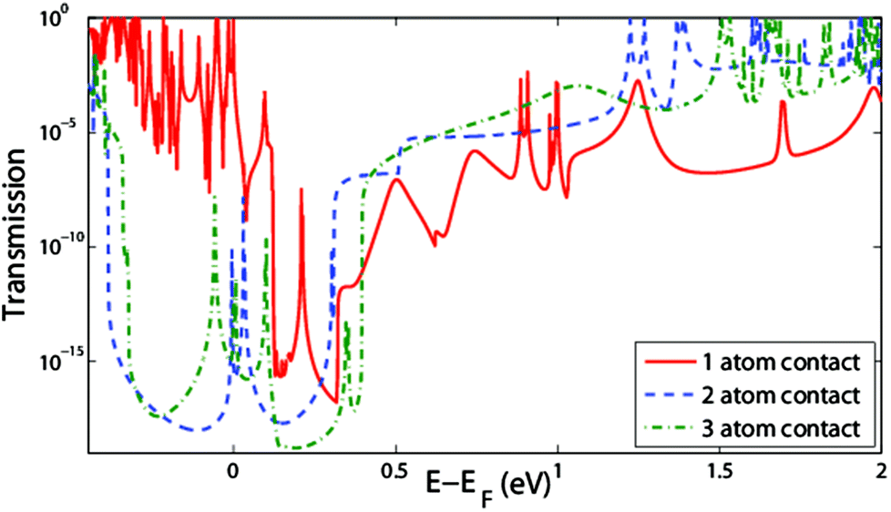 | ||
| Fig. 4 Transmission of a straight DB loop coupled to graphene nanoribbon electrodes terminated with (a) one (solid line in red), (b) two (dashed line in blue) and (c) three (dotted-dashed line in green) carbon atoms. In (b) and (c) the transmission around EF is much lower with respect to case (a) due to the state localization at the interface between graphene nanoribbon leads and DBs. | ||
For the sake of clarity, we limit our following discussion to the case where a single carbon atom of the nanoribbon couples to a single atom on the Si DB loop, which corresponds to Fig. 3a. The nanoribbon slices for the decimation procedure in the Lopez–Sancho algorithm23 were taken at a distance of a few dimer rows away from the central part – including not only Si atoms, but also the first few atoms of the nanoribbon tip – in order to minimize the influence on the DB states. This, together with periodic boundary conditions, forced us to take a large substrate eight Si atoms thick, nine atoms wide and eight dimer rows long in the transport direction.
The difference in DOS between zigzag and straight loops eventually leads to a higher transmission (and current) for zigzag topology, comparing panels (a) and (b) in Fig. 5. In the case of a straight loop the DB states are mainly created below the Fermi energy in a smaller energy window (∼0.16 eV) closer to the conduction band. The corresponding transmission displays therefore a very asymmetric behavior around the Fermi energy with strong suppression of the conductance already a few meV above the Fermi level (Fig. 5a).
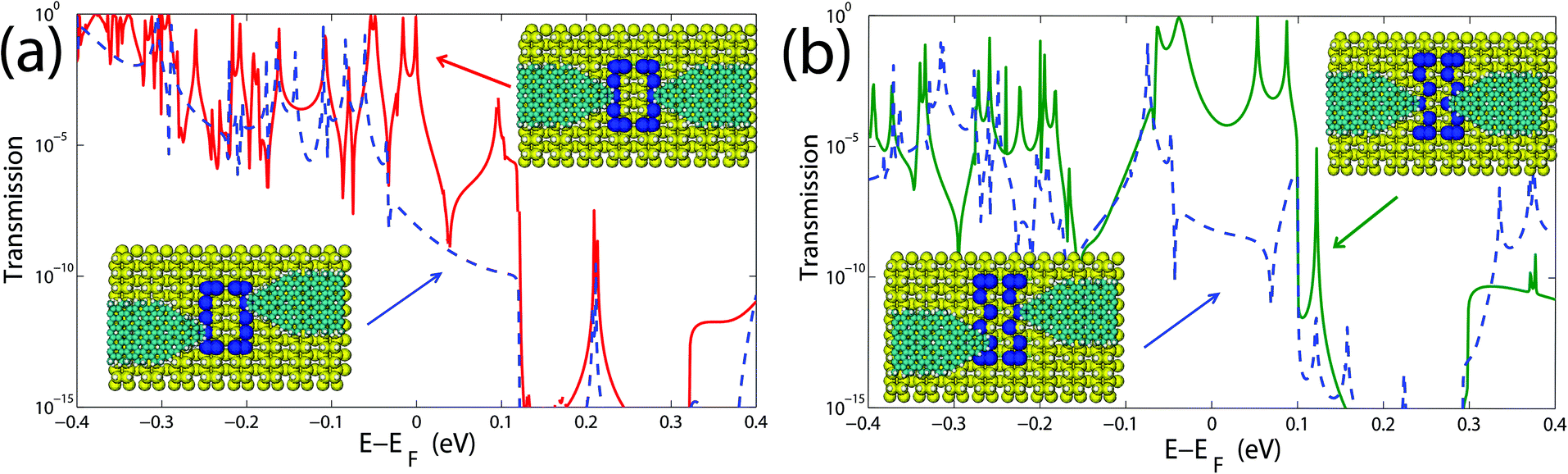 | ||
| Fig. 5 The quantum mechanical transmission functions at low energies, i.e. around EF, for (a) straight and (b) zigzag DB loops. The dashed lines in both cases indicate the asymmetric connection of the DB loops to the graphene nanoribbons, see also the corresponding insets illustrating the different nanribbon–DB loop–nanoribbon contact configurations. | ||
Since DB loops form a close contour, one could expect to have a Mach–Zehnder like interferometer supported by the conducting surface states. Within a semi-classical picture, electrons that enter the DB loop following different trajectories clockwise or counterclockwise have different phases when they reach the opposite lead. This may result in constructive or destructive interference effects, depending on the path the electron propagates. This effect might be expected only if the DB states take part in the transport, while tunneling between the loop side arms through the substrate will destroy any interference. Such quantum interference effects can be best revealed by varying the contact position between one of the electrodes and the DB loop, which could be implemented by the tip of an STM. Note that these interference effects are induced and controlled by changes in the global geometrical arrangement of the electrode plus DB system, in contrast to magnetic field induced interference effects of the Aharonov–Bohm type, as demonstrated e.g. in Si nanorings.34
In Fig. 5 we show the effect of symmetric (solid line) and asymmetric (dashed line) coupling of the leads on the transmission function for straight (c) and zigzag (d) DB loops. In the case of asymmetric coupling, transport around the Fermi energy is dramatically suppressed for both topologies due to interference effects involving the DB electronic states. This can be rationalized based on previous studies in ref. 38 and 39, where it was shown that for coherent transport the conductance of two nanoscale wires in parallel with no phase shift and a common junction to the electrodes is proportional to the sum of the individual conductances plus a quantum mechanical term containing constructive interference: 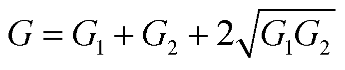 . However, introducing a phase shift leads to destructive interference. A similar situation holds in our case, where the two branches of the DB loop can be seen as two molecular wires. Although in the continuum limit the pathways for electrons moving clockwise and anti-clockwise have the same length for the symmetric and asymmetric arrangements of the electrodes, they clearly differ in an atomistic picture due to the different values of the electronic couplings along rows and between rows. As a result, the term
  will be different for the two electrode arrangements and destructive interference can induce a suppression of the transmission for states with a strong contribution from DB surface states.
The ratio between the transmissions for the symmetric and asymmetric coupling geometries can be as large as 105. On the contrary, for energies farther away from the Fermi level the transmission is considerably less affected, since the corresponding electronic states have a stronger bulk character.
Interference effects can become more pronounced when tuning the electron phase by increasing the surface area of the DB loop. So far we have calculated the electronic and transport properties of the full system that includes the DB loop and part of the substrate as depicted in Fig. 3. However, modeling of larger loops becomes increasingly demanding from the computational point of view, so that instead of inverting large matrices to get the corresponding Green's functions, we use numerically efficient recursive Green's function techniques.33 Details of the implementation are provided in the ESI.†
Progressively changing the length of the loop along the (100) surface direction is mapped then onto a change in the number of slices Ny in the recursive Green's function algorithm. Each slice contains the dangling bond atoms belonging to a full row of the loop as well as the substrate atoms underneath. The influence of the loop length can first be illustrated with a minimal tight-binding model shown in the top left panel of Fig. 6, which mimics the coupling between silicon pz states along the loop. There are three different nearest-neighbor electronic hopping parameters t1, t2, and t3 related to the three different types of sites we have in the loop, see the inset in the upper left panel of Fig. 6. Taking t1 = 0.028 eV as computed within the DFTB code, we chose t1/t2 = 1.5, and t2/t3 = 2.1, see also ref. 32. The leads are assumed for simplicity to be tight-binding square lattices. As shown in Fig. 6 (upper left panel), there is a clear beating-like effect in the transmission as a function of the loop length (number of slices) Ny, reflected in the short-range odd–even oscillations and long-range modulation of the profile.
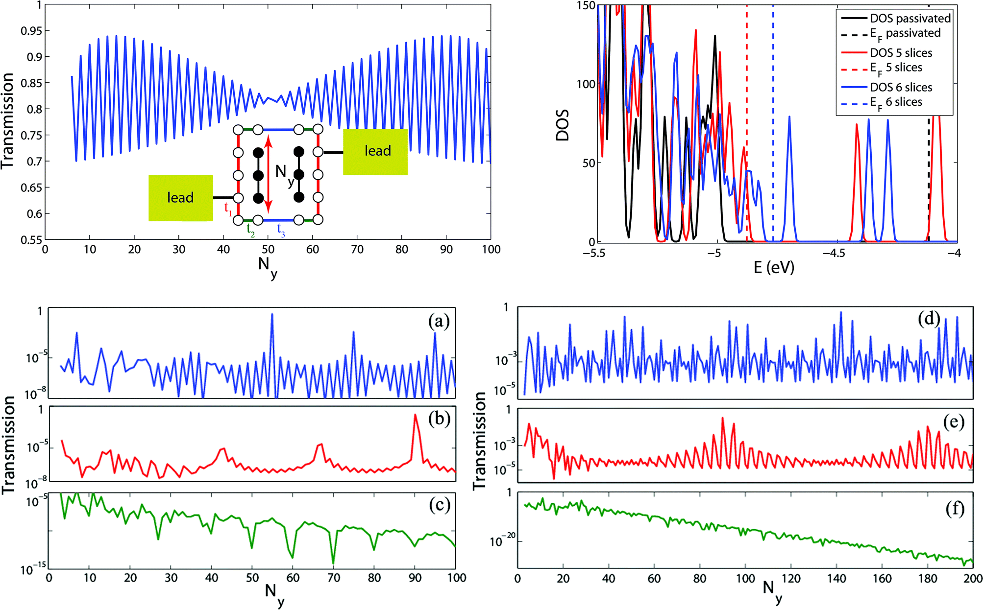 | ||
| Fig. 6 Top left panel: transmission function as a function of the loop length Ny at a fixed energy (on resonance) for the minimal tight binding model described in the text. The left and right electrodes are assumed to be tight-binding square lattices. Top right panel: electronic DOS for a realistic rectangular DB loop for two different numbers of slices (loop lengths along the dimer rows): five (red) and six (blue). For reference also the DOS of a fully passivated surface is shown. Note that there is a state at the Fermi level (∼−4.9 eV) for the odd-number loop, while no states are present at the corresponding Fermi energy (∼−4.8 eV) for an even number of slices. This behaviour leads to the short-range odd–even oscillations of the transmission function as a function of the loop length (as far as the chosen energy is on or close enough to a resonance). Bottom panel: typical transmission functions through the straight (a, b, c) and zigzag (d, e, f) DB loops, as a function of the loop length Ny, calculated near the Fermi energy at (a) E − EF = −0.02 eV, (b) −0.027 eV, (c) −0.01 eV, (d) −0.05 eV, (e) 0.05 eV, and (f) E = EF. | ||
Concerning first the short period odd–even oscillations, there is a general argumentation that has been used over the past few years to explain the presence of odd–even oscillations in atomic chains and molecular wires.35–37 For not too strong coupling to the electrodes, the maxima of the transmission function are located at the position of the eigenstates of the decoupled (from the electrodes) system. For a system like a linear atomic chain with N sites one finds that in the case when N is odd there is always a level in the spectrum at the Fermi energy leading to a maximum in the linear conductance. On the contrary, when N is even there is no level at the Fermi energy and therefore the system exhibits a considerably lower conductance. For realistic dangling bond loops, we find a very similar behavior, as shown in the electronic DOS plot for a straight DB loop in the upper right panel of Fig. 6. There two cases with five and six DB slices, respectively, are depicted. Note that we have in this case two different Fermi energies (vertical dashed lines) of the whole system. One can clearly see that for five slices a state appears almost on top of the Fermi energy (∼−4.9 eV), while for six slices no states are located at the corresponding Fermi level (∼−4.8 eV). This behavior will eventually lead to short-range odd–even oscillations of the transmission shown in the bottom panel of Fig. 6. Panels a, b and c show the results for straight loops and panels d, e and f show the results for zigzag loops. Here, for both the arrangements, odd–even oscillations are clearly seen if we fix the energy near a transmission resonance of the corresponding system, as shown in panels a, b, d and e in Fig. 6. However, by choosing an energy in between two transmission resonances (virtual tunneling), we obtain an exponential decrease of the transmission with increasing Ny, as illustrated in panels c and f of Fig. 6. Note that the transmission in panels a, b, d and e may differ by more than a factor of 105.
Turning now to the long-range modulation of the transmission, direct analytical results for our tight-binding model are not feasible due to the lack of periodicity, which precludes a direct diagonalization by going to the k-space. Hence, we have studied a very simple ladder model which allows for exact analytical expressions and which goes into the loop geometry if the internal coupling between sites located on different strands of the ladder goes to zero with the exception of the terminal sites (details of the model are included in the ESI†). The main result is that a beating-like effect, characterized by two typical wavelengths, can be found: the shorter length scale is related to the lattice spacing in the tight-binding representation and does not depend either on the energy of the incoming electron or on the details of the electronic structure (hopping parameters), while the longer one, modulating the short-range oscillating transmission as a function of the length, does depend in a non-trivial way on the different electronic coupling parameters as well as on the incoming electron energy. The fact that we also find a similar qualitative beat-like behavior in the realistic DB loop configuration (see the panels a, b, d and e of Fig. 6) suggests that this effect is quite robust and less sensitive to details of the atomistic and electronic structures.40
4. Conclusions
In summary, we have addressed from an atomistic perspective, charge transport signatures of dangling-bond loops in contact with mesoscopic graphene nanoribbons on an otherwise H-passivated Si(100) surface. Loops built up with a zigzag arrangement of depassivated silicon atoms along the rows display by far a better low-energy (around the Fermi level) conductance when compared to the straight arrangement. Nevertheless, the strong asymmetry of the transmission around the Fermi level found in the latter case may have interesting consequences for the thermopower of the system, which is, in the first approximation, determined by the behavior of the first derivative of the transmission around the Fermi level of the system. Addressing this issue requires, however, a separate study. Fingerprints of quantum interference effects in the transmission function for different loops have been demonstrated to sensitively depend on the connecting site of the electrodes to the DB loop. Moreover, the conductance of the loop does depend in a non-trivial way on the number of the terminal carbon atoms in the electrodes contacting the DB loop. Our results have also shown that quantum interference effects are only related to DB electronic states, so that their manipulation may allow for an additional control strategy of the electrical transport, since variations in the linear conductance of several orders of magnitude could be realized. This may be implemented by changing the position of one of the leads, e.g. by using instead of a second graphene nanoribbon a functionalized STM tip, or by applying a voltage between different leads in a multi-terminal setup. Our investigation hints at the possibility of exploiting such effects in loop topologies for the design of planar-based atomic-scale electronics and its application for e.g. implementing logic gates.Acknowledgements
This work was partly funded by the EU within the projects Planar Atomic and Molecular Scale devices (PAMS, project nr. 610446). This work has also been partly supported by the German Research Foundation (DFG) within the Cluster of Excellence “Center for Advancing Electronics Dresden”. Computational resources were provided by the ZIH at the Dresden University of Technology.References
- C. Joachim, J. Gimzewski and A. Aviram, Nature, 2000, 408, 541 CrossRef CAS PubMed.
- S. Godlewski, M. Kolmer, H. Kawai, B. Such, R. Zuzak, M. Saeys, P. de Mendoza, A. M. Echavarren, C. Joachim and M. Szymonski, ACS Nano, 2013, 7, 10105 CrossRef CAS PubMed.
- D. R. Bowler, J. Phys.: Condens. Matter, 2004, 16, R721 CrossRef CAS.
- R. A. Wolkow, L. Livadaru, J. Pitters, M. Taucer, P. Piva, M. Salomons, M. Cloutier and B. V. Martins, Field-Coupled Nanocomputing, Springer, 2014, pp. 33 Search PubMed.
- C. Joachim, D. Martrou, M. Rezeq, C. Troadec, D. Jie, N. Chandrasekhar and S. Gauthier, J. Phys.: Condens. Matter, 2010, 22, 084025 CrossRef CAS PubMed.
- J. Owen, K. Miki and D. Bowler, J. Mater. Sci., 2006, 41, 4568 CrossRef CAS.
- J. C. Cuevas and E. Scheer, Molecular Electronics: An introduction to Theory and Experiment, World Scientific, 2010 Search PubMed.
- S. J. van der Molen and P. Liljeroth, J. Phys.: Condens. Matter, 2010, 22, 133001 CrossRef PubMed.
- S. R. Schofield, P. Studer, C. F. Hirjibehedin, N. J. Curson, G. Aeppli and D. R. Bowler, Nat. Commun., 2013, 4 CAS , 1649.
- M. Y. Simmons, Nat. Phys., 2008, 4, 165 CrossRef CAS.
- M. Kepenekian, R. Robles, C. Joachim and N. Lorente, Nano Lett., 2013, 13, 1192 CrossRef CAS PubMed.
- B. Naydenov and J. J. Boland, Nanotechnology, 2013, 24, 275202 CrossRef PubMed.
- M. B. Haider, J. L. Pitters, G. A. DiLabio, L. Livadaru, J. Y. Mutus and R. A. Wolkow, Phys. Rev. Lett., 2009, 102, 046805 CrossRef PubMed.
- J. Y. Lee, J.-H. Cho and Z. Zhang, Phys. Rev. B: Condens. Matter, 2009, 80, 155329 CrossRef.
- C. Bird and D. Bowler, Surf. Sci., 2003, 531, L351 CrossRef CAS.
- S. C. Erwin and F. Himpsel, Nat. Commun., 2010, 1 CAS , 584.
- M. Kepenekian, F. D. Novaes, R. Robles, S. Monturet, H. Kawai, C. Joachim and N. Lorente, J. Phys.: Condens. Matter, 2013, 25, 025503 CrossRef PubMed.
- R. Robles, M. Kepenekian, S. Monturet, C. Joachim and N. Lorente, J. Phys.: Condens. Matter, 2012, 24, 445004 CrossRef CAS PubMed.
- L. Soukiassian, A. J. Mayne, M. Carbone and G. Dujardin, Surf. Sci., 2003, 528, 121 CrossRef CAS.
- E. Rauls, J. Elsner, R. Gutierrez and T. Frauenheim, Solid State Commun., 1999, 111, 459 CrossRef CAS.
- A. Pecchia, G. Penazzi, L. Salvucci and A. Di Carlo, New J. Phys., 2008, 10, 065022 CrossRef.
- S. Datta, Electronic transport in mesoscopic systems, Cambridge University Press, 1997 Search PubMed.
- M. L. Sancho, J. L. Sancho, J. L. Sancho and J. Rubio, J. Phys. F: Met. Phys., 1985, 15, 851 CrossRef.
- H. Kawai, F. Ample, Q. Wang, Y. K. Yeo, M. Saeys and C. Joachim, J. Phys.: Condens. Matter, 2012, 24, 095011 CrossRef PubMed.
- F. Ample, I. Duchemin, M. Hliwa and C. Joachim, J. Phys.: Condens. Matter, 2011, 23, 125303 CrossRef CAS PubMed.
- M. Kittelmann, P. Rahe, M. Nimmrich, C. M. Hauke, A. Gourdon and A. Khnle, ACS Nano, 2011, 5, 8420 CrossRef CAS PubMed.
- C. Jinming, R. Pascal, J. Rached, B. Marco, B. Thomas, B. Stephan, M. Matthias, P. S. Ari, S. Moussa, F. Xinliang, M. Klaus and F. Roman, Nature, 2010, 466, 470 CrossRef PubMed.
- G. Lopinski, D. Wayner and R. Wolkow, Nature, 2000, 406, 48 CrossRef CAS PubMed.
- Y. Xu, K. He, S. Schmucker, Z. Guo, J. Koepke, J. Wood, J. Lyding and N. Aluru, Nano Lett., 2011, 11, 2735 CrossRef CAS PubMed.
- K. A. Ritter and J. W. Lyding, Nat. Mater., 2009, 8, 235 CrossRef CAS PubMed.
- P. M. Albrecht, S. Barraza-Lopez and J. W. Lyding, Small, 2007, 3, 1402 CrossRef CAS PubMed.
- H. Kawai, F. Ample, Q. Wang, Y. K. Yeo, M. Saeys and C. Joachim, J. Phys.: Condens. Matter, 2012, 24, 095011 CrossRef PubMed.
- G. Metalidis and P. Bruno, Phys. Rev. B: Condens. Matter, 2005, 72, 235304 CrossRef.
- T. C. G. Reusch, A. Fuhrer, M. Fchsle, B. Weber and M. Y. Simmons, Appl. Phys. Lett., 2009, 95, 032110 CrossRef.
- R. Gutiérrez, F. Grossmann, O. Knospe and R. Schmidt, Phys. Rev. A, 2001, 64, 013202 CrossRef.
- N. D. Lang and P. Avouris, Phys. Rev. Lett., 2000, 84, 358 CrossRef CAS PubMed.
- V. Mujica, M. Kemp and M. A. Ratner, J. Chem. Phys., 1994, 101, 6856 CrossRef.
- C. Joachim, Nat. Nanotechnol., 2012, 7, 620621 CrossRef PubMed.
- M. Magoga and C. Joachim, Phys. Rev. B: Condens. Matter, 1999, 59, 16011 CrossRef CAS.
- Related results for the I–V characteristics of the DB loops with variable sizes can be found in Fig. S6 and S7 of the ESI.†.
Footnote |
| † Electronic supplementary information (ESI) available: Simulation details of different carbon nanoribbon leads coupled to the DB loops and technical details related to the recursive Green function approach used to model DB loops with variable size. See DOI: 10.1039/C5NR01251A |
| This journal is © The Royal Society of Chemistry 2015 |