
 Open Access Article
 This Open Access Article is licensed under a
 Creative Commons Attribution 3.0 Unported Licence
Templating growth of gold nanostructures with a CdSe quantum dot array
Neelima
Paul
*a,
Ezzeldin
Metwalli
b,
Yuan
Yao
b,
Matthias
Schwartzkopf
c,
Shun
Yu
cd,
Stephan V.
Roth
c,
Peter
Müller-Buschbaum
b and
Amitesh
Paul
*e
aTechnische Universität München, Heinz Maier-Leibnitz Zentrum (MLZ) Lichtenberg Strasse 1, 85748 Garching, Germany. E-mail: neelima.paul@frm2.tum.de
bTechnische Universität München, Physik-Department, Lehrstuhl für Funktionelle Materialien, James-Franck-Str. 1, 85748 Garching, Germany
cDeutsches Elektronen-Synchrotron DESY, Notkestr 85, 22607 Hamburg, Germany
dRoyal institute of Technology (KTH), Teknikringen 56-58, SE-10044 Stockholm, Sweden
eTechnische Universität München, Physik Department, Lehrstuhl für Neutronenstreuung, James-Franck-Strasse 1, 85748 Garching, Germany. E-mail: amitesh.paul@frm2.tum.de
First published on 30th April 2015
Abstract
In optoelectronic devices based on quantum dot arrays, thin nanolayers of gold are preferred as stable metal contacts and for connecting recombination centers. The optimal morphology requirements are uniform arrays with precisely controlled positions and sizes over a large area with long range ordering since this strongly affects device performance. To understand the development of gold layer nanomorphology, the detailed mechanism of structure formation are probed with time-resolved grazing incidence small-angle X-ray scattering (GISAXS) during gold sputter deposition. Gold is sputtered on a CdSe quantum dot array with a characteristic quantum dot spacing of ≈7 nm. In the initial stages of gold nanostructure growth, a preferential deposition of gold on top of quantum dots occurs. Thus, the quantum dots act as nucleation sites for gold growth. In later stages, the gold nanoparticles surrounding the quantum dots undergo a coarsening to form a complete layer comprised of gold-dot clusters. Next, growth proceeds dominantly via vertical growth of gold on these gold-dot clusters to form an gold capping layer. In this capping layer, a shift of the cluster boundaries due to ripening is found. Thus, a templating of gold on a CdSe quantum dot array is feasible at low gold coverage.
Introduction
Quantum dots attract much interest because they exhibit size-dependent optical and electronic properties.1,2 Semiconductor quantum dot arrays have several potential applications in nanoelectronics and optoelectronics, for example, in lasers, next generation solar cells, light emitting diodes, quantum computation.3 For example, CdSe quantum dots are chemically stable and highly luminescent in the entire visible light range therefore several CdSe-based quantum dot solar cells have been fabricated during the recent years.4–6 For the aforementioned optical applications, a sharp size distribution and a long range ordering of the quantum dots is beneficial, because this leads to a more uniform emission spectrum. However, there is only little information on ordering and correlation effects, which is desirable for many device applications.7 It is to be noted that CdSe quantum dots are rather small, and due to strong intermixing during overgrowth by other II–VI semiconductors they exhibit a diminished chemical contrast. Therefore, the detection of such rather weak compositional fluctuations and their correlation is experimentally challenging.8 Gold has a sufficient chemical contrast to CdSe and therefore is a suitable material for overgrowth and for monitoring correlation effects of gold growth on CdSe quantum dot templates.Growth of gold on electronically active materials like semiconductors is also of extreme interest in research involving field effect transistors, light emitting diodes and solar cells.9–11 In the latter, the preferred metal contacts are usually gold, silver and aluminum. In conventional solar cells, the role of thin metallic films is to allow the easy passage for charge carriers whereas in tandem solar cells, they can also serve as charge recombination centers between the single junctions.12,13 Thus, growth of metals such as gold on semiconductors and their mutual interactions are interesting from the viewpoint of electronic devices as well. Growth of gold nanostructures itself is relevant in various aspects of nanotechnology due to its size dependent properties.14–17
Observation of gold growth on quantum dot array templates can also shed light on other fundamental aspects such as quantum confinement because of the large interface between the cluster and the surrounding medium. For instance, when quantum dots are surrounded by materials having much lower refractive indices (in the optical regime) like gold, the field intensity at the interface or surface can be enhanced considerably as compared to the incident intensity. Such an enhancement in the local field is a consequence of the dielectric confinement effect and can be an important factor in describing the spectroscopy, photophysics and nonlinear optics of these clusters.18,19 A study of the growth mechanism and morphological evolution of gold modified CdSe quantum dots can thus be useful for testing the theories of quantum confinement and obtaining particles with special spectroscopic properties.
Grazing incidence small-angle X-ray scattering (GISAXS) has proven to be a powerful tool to analyze the spatial organization and size distribution of buried particles having dimensions in the nanometer range.20,21 Due to the increase in source brilliance at third generation synchrotron radiation sources, real-time GISAXS measurements became accessible.22 For example, using the real-time GISAXS technique, it became possible to systematically monitor the growth behavior and corresponding morphological evolution of metal layers in situ during sputter deposition.23–26 The high time resolution (milliseconds) of such real-time experiments allowed for determination of kinetics of initial nucleation as well as the subsequent clustering towards a compact layer. Typically growth laws were identified, which deepened the understanding of morphology formation.
In the present work, we expand the investigation about thin metal nanolayers formed during sputter deposition. We investigate the mechanism of gold nanostructure growth on a tailored CdSe quantum dot array to probe the templating possibilities. Real-time GISAXS experiments are used to follow the different stages of gold nanomorphology evolution during sputter deposition. This well-organized quantum dot array serves as a model template for investigating growth of gold nanostructures with in situ and real-time GISAXS experiments.
Experimental section
Template synthesis
The CdSe quantum dots dispersed in toluene were obtained from Bayer Technology Services, Germany. Passivating ligands like trioctylphosphine (TOP) and oleic acid (OA) were used in the synthesis to avoid agglomeration and preserve the confinement of charges. A thin layer of CdSe quantum dots was prepared on clean SiO2 substrates by dip coating using a constant withdrawal speed of 1 mm s−1 under an inert atmosphere as described elsewhere in detail.27 The resulting quantum dot array was used in the gold sputter deposition. For transmission electron microscopy (TEM) measurements, the OA and TOP capped quantum dots were prepared by dipping a polymer coated copper grid into a highly diluted suspensions of CdSe quantum dots in a manner similar to a previous study by Zillner et al.28Transmission electron micrographs were used to determine the quantum dot size, inter-dot distances and their distributions over a local area. Measurements were done on a Philips CM12 Transmission Electron Microscope operating an accelerating voltage of 120 kV and a LaB6cathode. Distances between the quantum dots were determined by manually measuring the distance between their centers and calculating an average value. Similarly, quantum dot size was measured manually on several quantum dots and averaged. For the thickness measurement, the sample was scratched with a non-hardened steel needle at 2 different places and the thickness was determined at ten different positions. Using a step profiler, the average quantum dot thickness was determined to be about 7 nm.
In situ sputtering GISAXS experiments were performed at the Micro- and Nanofocus X-ray scattering (MiNaXS) beamline P03 of the high brilliance light source PETRA III at DESY, Hamburg.29 Gold was deposited by vacuum sputter deposition technique using a 99.999% gold target(from MaTecK GmbH). The sputter deposition was performed at room temperature for 600 s in Ar gas atmosphere at a pressure of 15 μbar and with an applied power of 100 W.
To calculate the final gold film thickness, gold was also grown on a bare Si substrate for 600 s. The corresponding X-ray reflectivity (XRR) data and its fit are shown in Fig. 1.
 | ||
| Fig. 1 X-ray reflectivity of Au covered Si substrate after 600 s deposition. | ||
From the model used for the XRR fit, a gold film thickness of dAu = 14.4 ± 1.7 nm, was extracted. Thus, the nominal sputter deposition rate was deduced to be 0.024 nm s−1. Sputtering conditions were selected with a very low deposition rate to enhance the gold nanoparticle surface diffusion and prevent any premature clustering in the gaseous phase so that gold can reach the quantum dot array in its atomic state.
A PILATUS 300 K detector (DECTRIS Ltd) with a readout time of 3.6 ms and the intense photon flux enabled the in situ and real-time investigation of gold growth during the sputter deposition with high acquisition throughput. The detailed experimental set-up is described in detail elsewhere.23,30 For all measurements, a wavelength of 0.09537 nm, an incident angle of 0.5° and a sample-detector distance of 2011 mm were used. A point-like beam stop was used to block the specularly reflected beam which would otherwise saturate the detector. Following the scattering geometry of a typical GISAXS set-up,31 the momentum transfer vector Q→ can be written as its various components:
 | (1) |
 | (2) |
 | (3) |
A two-dimensional intensity map is measured after the X-ray beam has been scattered from the sample. The scattered intensity is, to the 1st order, proportional to the square of the particle form factor times the interference function.32,33 The particle form factor is the Fourier transform of the particle shape whereas the interference function is the Fourier transform of the particle–particle pair correlation function describing the particle distribution in the sample.
Modeling for treating the GISAXS data
For the analysis of the static GISAXS data modeling was done using an effective surface approximation (ESA) approach (assuming spheres as scattering objects). The statistically averaged sphere size, inter-sphere distance as well as their size and distance distribution using Gaussian functions (denoted as size/distance ± sigma distribution) were extracted. The interference function was based on a one-dimensional paracrystal model which can be described by a regular one-dimensional lattice having a cumulative loss of long range order.34 In the applied modeling of the intensity of the one-dimensional horizontal line cuts (along Qy at a particular Qz position the contribution from the spheres along the Qz direction (corresponding to the height of the spheres) was neglected.31 For very low Qy values, the experimental resolution limit of the instrument was taken into account and modeled using a Lorentzian-shaped function. IsGISAXS was used for simulation of the measured two-dimensional (2D) GISAXS patterns.32For the analysis of the time-resolved GISAXS data, one-dimensional line cuts were taken using the full time resolution to extract information on the kinetics of gold growth. The ESA was used again for fitting the horizontal line cuts with Lorentzian distribution functions.35 Diffuse scattering with GISAXS includes a Qy resolution which increases the complexity of experimental interpretation. Thus, approaches like ESA are used for simplification of the scattering cross-section within the distorted wave born approximation (DWBA). The differential cross-section includes the diffuse scattering intensity which is dominated by the Fourier transform of the height–height correlation function of only one effective surface hence ‘ESA’.36 In this way, the diffuse scattering factor is approximated to depend on the form factor of the individual objects and also on the structure factor. The temporal evolution of the peak position and peak width enabled us to track the relevant structural changes occurring in the gold thin film during sputter deposition.23,37
Results and discussion
Quantum dot array: before and after gold nanostructure growth
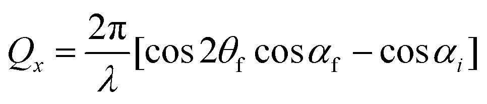
Fig. 2(a) shows a transmission electron micrograph of the CdSe quantum dot array and Fig. 2(b) presents a magnified TEM view of a single CdSe quantum dot. The typical wireframe outline of a model quantum dot is depicted in Fig. 2(c). The diameter of a single quantum dot as measured from the TEM images is 4.5 ± 0.5 nm. The quantum dot array shows a well-defined distribution of the quantum dots with a distance of 7.7 ± 0.2 nm between centers of the neighboring quantum dots. The CdSe crystallites within the quantum dot (in Fig. 2(b)) show atomic columns with hexagonal arrangement indicating an [0001] orientation of the CdSe dot (the inter-atomic distance being equal to the lattice parameter ‘a’ of the wurtzite structure). Such a regular hexagonal arrangement of CdSe quantum dots has also been observed during another study on shape control of CdSe nanocrystals.39 Recently, well-organized hexagonal ordering of similar dimensions has also been reported for PbSe quantum dots.40 | ||
| Fig. 2 (a) TEM image of CdSe quantum dot array, (b) enlarged TEM view of a single CdSe quantum dot oriented along the (001) axis, (c) wireframe outline of a model crystallite. This image has been reproduced from ref. 38 with permission. | ||
Complementary to TEM, which measures the local morphology of a very small part of the quantum dot array, GISAXS probes the large scale morphology with a high statistical relevance. GISAXS is performed to investigate if the observed surface morphology extends over the entire array and within the inner film volume. Thus, GISAXS measurements can deliver statistically averaged values for the quantum dot radius and inter-dot distance, which are representative of the whole array.
Fig. 3(a) shows the two-dimensional GISAXS data of the bare quantum dot array where some pronounced features such as Yoneda peak, peaks due to lateral and vertical correlations are highlighted. The circular black shielding is due to the Pb beam stop which is mounted to prevent detector saturation from the intense specular beam. The horizontal black line is the inter-module gap of the Pilatus detector. The material characteristic Yoneda peak (Y1), causing a maximum in the scattered intensity, is located below the specular peak at Qy = 0 nm−1. One very intense peak due to a lateral correlation (or the 1st order lateral correlation peak), indicated by a white arrow (i), is visible at Qy = 0.92 nm−1 at Qz = 0.75 nm−1. It arises from the in-plane nearest-neighbor short-range ordering of the CdSe quantum dots. A faint 1st order scattering maximum (or the vertical correlation peak), indicated by the dashed white ellipse (iii), can be noticed directly above this peak due to a vertical correlation in the dots. This is usually an indication of a nearly uniform height of the quantum dots with only small variances.25 Another weaker lateral correlation peak (2nd order) seen at Qy = 1.8 nm−1 and indicated by a white arrow (ii), shows the extension of the short range ordering to the next-nearest-neighbor level. For this lateral correlation peak as well, a faint 2nd order scattering maximum (iv) in the vertical direction (but at a lower Qy = 1.62 nm−1) value can be seen.
 | ||
| Fig. 3 Two-dimensional GISAXS data of the quantum dot array (a) before and (c) after gold deposition are shown along with simulated GISAXS patterns (b) before and (d) after gold deposition. Characteristic structures are highlighted and explained in the text. (e) One-dimensional vertical line cuts along Qy = 0 nm−1 before (bottom curve) and after (top curve) gold deposition are shown with highlighted Yoneda peak positions Y1 and Y2. (f) One-dimensional horizontal line cuts (solid black rectangles) across the Yoneda maximum before (bottom curve) and after (top curve) gold deposition are shown together with their fits (red lines) using a model as described in the text. At the top, a schematic shows the side-view morphology of the quantum dot array before and after gold deposition. | ||
Three distinct features (a) appearance of the 2nd order vertical correlation peak (iv) at a lower Qy value (as compared to the Qy position of the 2nd order lateral correlation peak (ii)), (b) the relative weak intensity of this height modulation and (c) a faint ring like halo are indications of a spherical shape of the quantum dots. A further inference on the shape of the quantum dots can be drawn by simulating the full two-dimensional intensity map using the IsGISAXS software. We considered various shape geometries such as spheres, hemispheres and cylinders with different aspect ratios in our modelling as can be seen in Fig. 4. The most reasonable agreement between the experimental data and the simulated two-dimensional GISAXS pattern is observed for a spheroidal shape geometry (Fig. 4(a)) which is shown also in Fig. 3(b). The main features of the two-dimensional GISAXS data such as the positions of the peaks due to the lateral correlation in Qy and the positions of the vertical correlation peaks in Qz at two different Qy positions are well reproduced in the simulation. The estimated height of the quantum dot from this model is around 5 nm.
 | ||
| Fig. 4 IsGISAXS simulations of the bare quantum dot template for a fixed dot radius R = 2.5 nm and various shapes and heights such as (a) sphere, (b) hemisphere, (c) cylinder H = 2R, (d) cylinder H = 2.5R, (e) cylinder H = 3R and (f) cylinder H = 3.5R. | ||
A one-dimensional vertical line cut of the two-dimensional GISAXS data along Qz is shown in Fig. 3(e). The Yoneda maximum (Y1) is located at a Qz value of 0.75 nm−1 corresponding to an experimental scattering length density (SLD) value of 2.22 × 10⁻⁵ Å−2. This SLD value is similar to the theoretical SLD value of SiO2(2.27 × 10⁻⁵ Å−2), which is the substrate for the quantum dot array. A one-dimensional horizontal line cut along Qy of the two-dimensional GISAXS data is shown in Fig. 3(f). The data is fitted with a model similar to that used in the IsGISAXS simulation. The most prominent size distribution extracted from this model corresponds to an average quantum dot diameter of 5.2 ± 0.2 nm and an average inter-dot spacing of 6.7 ± 0.3 nm. These values are in good agreement with those obtained from the TEM measurements.
After completion of the gold deposition, the sample is again investigated with GISAXS. The two-dimensional GISAXS data of the quantum dot array after gold deposition is shown in Fig. 3(c). As compared to the GISAXS data of the bare quantum dot array, the 1st order lateral correlation peak has shifted to a lower Qy position, indicated by a white arrow (v). This shift is attributed to the formation of a new surface morphology during the gold deposition. An enhancement of the scattering intensity below the circular beam stop (noticeable also in Fig. 3(e)) is due to presence of an additional Yoneda peak (Y2) of gold–CdSe being located at a higher Qz value. Above the circular beam stop, the intensity increases due to the Kiessig oscillation, which originate from the finite thickness of the thin gold film on the quantum dot array.
Based on IsGISAXS, the simulated two-dimensional GISAXS pattern for the quantum dot array after gold deposition is shown in Fig. 3(d). The model assumes a mixed gold–CdSe (50![[thin space (1/6-em)]](https://www.rsc.org/images/entities/char_2009.gif) :50) layer of 5 nm thickness having a high roughness with 11 nm thick gold hemispherical clusters on top. The main feature of the two-dimensional GISAXS data such as the lateral correlation peak (v) position in Qy is again well reproduced in the simulation. The estimated height of the gold capped quantum dot array from this model is 16 nm. The one-dimensional horizontal line cut is fitted with the model similar to that used in the IsGISAXS simulation. The most prominent size distribution extracted from this model corresponds to an average particle diameter of 5.4 ± 0.3 nm and an average inter-particle spacing of 10.0 ± 1.2 nm. The scattering signal from the initial long range distribution of the quantum dot arrangement is now dominated by the signal from the arrangement of the gold clusters, which does not replicate the morphology of the initial regular quantum dot arrangement. Moreover, the initially observed 2nd order peak due to the lateral correlation has disappeared. This demonstrates a loss in the long range order of the newly formed structure.
:50) layer of 5 nm thickness having a high roughness with 11 nm thick gold hemispherical clusters on top. The main feature of the two-dimensional GISAXS data such as the lateral correlation peak (v) position in Qy is again well reproduced in the simulation. The estimated height of the gold capped quantum dot array from this model is 16 nm. The one-dimensional horizontal line cut is fitted with the model similar to that used in the IsGISAXS simulation. The most prominent size distribution extracted from this model corresponds to an average particle diameter of 5.4 ± 0.3 nm and an average inter-particle spacing of 10.0 ± 1.2 nm. The scattering signal from the initial long range distribution of the quantum dot arrangement is now dominated by the signal from the arrangement of the gold clusters, which does not replicate the morphology of the initial regular quantum dot arrangement. Moreover, the initially observed 2nd order peak due to the lateral correlation has disappeared. This demonstrates a loss in the long range order of the newly formed structure.
One-dimensional vertical cuts at Qy = 0.92 nm−1 and Qy = 1.62 nm−1, corresponding to the first and second order vertical correlation peaks, both before and after gold deposition, are shown in Fig. 5. From the distance between the two adjacent vertical maxima (ΔQz), an average thickness of the Au layer on top of the quantum dot layer was extracted as 11.5 ± 0.4 nm using the simple approach based on eqn (4):
 | (4) |
 | ||
| Fig. 5 One-dimensional vertical line cuts for the entire Qz range for (a) 1st order vertical correlation peak (iii) located at Qy = 0.92 nm−1 and (b) 2nd order vertical correlation peak (iv) located at Qy = 1.62 nm−1, before (black) and after (red) gold deposition on the quantum dot array. Due to the higher scattering length density of the CdSe–gold layer, the maximal Qz position has shifted (along with the Yoneda maximum) from 0.75 nm−1 to 0.94 nm−1 after gold deposition. | ||
This thickness value differs from that extracted from the XRR measurement of gold on bare Si substrate (14.4 ± 1.7 nm). However, it may be noted that only with XRR the film thickness is probed directly along the Qz direction (⊥r to the film-plane), whereas the vertical line cuts along Qz in GISAXS measurements have an offset with the axes ⊥r to the sample plane. Thus, the intensity modulations along Qz are not the same for the XRR and GISAXS geometries. Moreover, gold growth on bare Si might differ in thickness from that on the quantum dot template.
Intermediate morphologies during gold sputtering
In order to understand how the initial quantum dot array is coated with gold in terms of the morphological evolution, a detailed in situ study is required. With time-resolved GISAXS, it is possible to follow the evolution of characteristic structures in situ during the gold sputter deposition.Two-dimensional GISAXS data are recorded during the gold deposition with a high time resolution to obtain full information about the gold growth on the quantum dot array. This template consists of two different materials, namely semiconductor CdSe quantum dots on an insulator SiO2matrix. As a consequence, it is interesting to investigate if the gold atoms have a preference for either of these two chemically different regions as nucleation sites for deposition. The observed growth process is spilt into two sections to separate the early stage of the dominating in-plane (horizontal) growth from the vertical growth at later stages.
 | ||
| Fig. 6 Selected two-dimensional GISAXS data from the in situ gold sputter deposition on the quantum dot array showing the early stages. Data are taken (a) before and during deposition for different gold thicknesses dAu: (b) 0.48 nm, (c) 0.96 nm, (d) 1.68 nm, (e) 2.16 nm, (f) 2.64 nm, (g) 3.12 nm and (h) 3.60 nm. | ||
 | ||
| Fig. 7 (a) Evolution of the peak broadening or full width at half maximum (FWHM) of the 1st order lateral correlation peak (i) as function of thickness dAu, along Qy (red open circles) as well as along Qz (black closed circles). Inset (a) Evolution of the 1st order (black closed circles) and 2nd order (red closed circles) lateral correlation peak positions with dAu. Note that the 2nd order peak due to lateral correlation disappears after dAu = 0.48 nm is reached. (b) Evolution of dot diameter and inter-dot spacing as function of dAu. | ||
The increase in the FWHM along Qz (black curve) indicates that there is a decrease in the vertical correlation length with increasing dAu. One can also observe a significant change in slope around dAu = 0.48 nm. A steeper slope is indicative of a stronger vertical correlation, typical of a growth maintaining the preferred nucleation sites. Above dAu = 0.48 nm, the initial preferred nucleation sites for the gold deposits (on top of the quantum dots) are gradually lost with the loss in the corresponding vertical correlation.
From Fig. 7(a), one can observe that the FWHM along Qy (red curve) of the 1st order peak remains constant only below an initial thickness, dAu of 0.48 nm. Above dAu = 0.48 nm, the FWHM of the peak shows an abrupt jump. This broadening indicates an increase in the distribution of size and inter-particle spacing. This can be visualized as due to gold nanoparticles positioning around the dots (and not only on the dots) and thereby increasing the effective size of the dots.
This trend can also be confirmed from the plot in Fig. 7(b), which shows the variation of the quantum dot size and the inter-dot spacing as a function of dAu. Below a thickness of about dAu = 0.48 nm both parameters remain fairly constant, which implies that the gold deposition is undergoing a change, which can be related purely to the height and not to lateral structures. An initial preferential accumulation of gold on top of the quantum dots is observed or in other words, gold nanoparticles perfectly decorate the quantum dots, maintaining the template structure. Above dAu = 0.48 nm no significant change in the dot diameter or the inter-dot spacing is seen up to dAu ≈ 2.5 nm. Thus, the increasing height does not affect the growth morphology in this regime. Above dAu ≈ 2.5 nm the dot diameter increases and the inter-dot distance decreases. These changes in both parameters signify the diffusion of gold–gold clusters – creating a cluster morphology different from the initial quantum-dot template.
Thus, initially there is an accumulation of gold atoms at and around the quantum dots (which act as preferred nucleation sites), followed by their lateral growth leading to a gradual coalescence and a systematic formation of a mixed gold-dot compact layer. The scattering length density (SLD) of Au is 12.46 × 10⁻⁵ Å−2, which is higher than the SLD value of CdSe (4.2 × 10⁻⁵ Å−2). As a consequence, with the successive accumulation of gold, an increase in the diffuse scattering from the sample surface is expected and is seen around Qy = 0 nm−1. Decoration of dots observed in the present work is in contrast to previous investigations, where in the GISAXS data, a peak due to lateral correlation constantly moves from far Qy values towards low values during metal deposition on either bare Si surface or on polymer films.23,41 In those studies, a random nucleation of gold nanoparticles on the solid surfaces was followed by lateral gold cluster growth, which initially had a smaller in-plane correlation length, but as growth proceeded and coalescence occurred, the in-plane correlation length increased and accordingly gold cluster related peak due to lateral correlations moved towards lower Qy values. In contrast, in the present study after the formation of mixed gold-dot particles, a characteristic scattering peak for a gold structure deviating from that of the quantum dots can not be traced.
 | ||
| Fig. 8 Selected two-dimensional GISAXS data from the in situ gold sputter deposition on the quantum dot array showing the late stages of growth. Data are taken during deposition for different thicknesses, dAu: (a) 4.8 nm, (b) 6.0 nm, (c) 7.2 nm, (d) 8.4 nm, (e) 10.8 nm, (f) 12.0 nm, (g) 13.2 nm and (h) 14.4 nm. | ||
In Fig. 9, selected one-dimensional vertical and horizontal line cuts are shown from the real-time study. For the X-ray wavelength used in the present experiment the critical angles of SiO2, CdSe and gold are 0.146°, 0.199°and 0.343°, respectively. These correspond to Qz values of 0.75 nm−1, 0.81 nm−1 and 0.97 nm−1, respectively according to the eqn (3), As mentioned earlier, the Yoneda peak for the quantum dot array on SiO2corresponds to an experimental SLD value of 2.22 × 10⁻⁵ Å−2. The second Yoneda peak which emerges after 200 s (see Fig. 9(a)) can be attributed to a mixed CdSe–gold layer having an experimental SLD value of 8.3 × 10⁻⁵ Å−2, which is exactly the average of the theoretical SLDs of CdSe (4.2 × 10⁻⁵ Å−2) and gold (12.4 × 10⁻⁵ Å−2) compact layers assuming a 50:50 composition. In Fig. 9(b), one observes thickness oscillations which appear at high Qz values and move towards lower Qz values with time (and dAu). In Fig. 9(c), one sees at an initial stage the prominent 1st order peak due to lateral correlation (dashed arrow I) from CdSe quantum dots. After dAu of 4.8 nm, another peak due to lateral correlation (dashed arrow II) starts to emerge and gradually moves to slightly lower Qz values with time.
 | ||
| Fig. 9 (a) One-dimensional vertical line cuts at Qy = 0 nm−1 for a selected Qz range (b) one-dimensional vertical line cuts at Qy = 0 nm−1 for the full Qz range and (c) one-dimensional horizontal line cuts at a constant Qz = 0.75 nm−1 for different thicknesses dAu: From bottom to top 0 nm, 1.2 nm, 2.4 nm, 3.6 nm, 4.8 nm, 6.0 nm, 7.2 nm, 8.4 nm, 9.6 nm, 10.8 nm, 12.0 nm, 13.2 nm and 14.4 nm. The arrows I and II indicate the characteristic lateral correlation peaks of the quantum dots and the gold nanostructures respectively. | ||
In Fig. 10, mappings extracted from the two-dimensional GISAXS data are shown to clarify the evolving structures. An overview of the temporal evolution of vertical and horizontal structures is gained from these maps. Fig. 10(a) and (b) show the time evolution of the vertical cuts taken at constant Qy = 0.92 nm−1 and at constant Qy = 0 nm−1, respectively. They exhibit temporal evolution of the structures perpendicular to the sample surface, which translates into its evolution with dAu. The thickness oscillations shown in Fig. 9(b) give rise to the oscillating intensity waves with varying Qz in Fig. 10(a) and (b).
 | ||
| Fig. 10 Mapping of vertical line cuts from the time-resolved two-dimensional GISAXS data taken at (a) Qy = 0.92 nm−1 and at (b) Qy = 0. (c) Mapping of horizontal line cuts from the time-resolved two-dimensional GISAXS data taken at the Yoneda maximum position. The solid white arrow follows the Au growth at quantum dots characteristic peak due to lateral correlation position. | ||
Fig. 10(c) represents the time evolution of the horizontal line cuts taken at the Yoneda peak with the full time resolution of the real-time experiment. In general, horizontal line cuts are sensitive to structural features parallel to a quantum dot array. Thus, Fig. 10(c) represent the temporal lateral structure evolution which translates into changes with increasing thickness dAu. The peak due to lateral correlation or intensity maxima at Qy = 0.92 nm−1, is very intense in the initial stages till dAu ≈ 3.6 nm, due to short range ordering of CdSe quantum dots. For larger dAu, its intensity gradually decreases and the scattering is dominated by the scattering from the compact gold layer which has formed on the template by this time. Subsequent deposition leads to nanoparticle cluster growth and coalescence in agreement with the behavior observed in studies on other systems.23,25,41
Growth model
The morphologic evolution of gold nanostructure growth on the quantum dot array is schematically depicted in Fig. 11. The regular arrangement of the quantum dots in the template causes peak due to lateral correlations (denoted with ‘i’ and ‘ii’ in Fig. 3(a)). In the early stages of growth, gold decorates preferentially the top of the quantum dots. Therefore, in this early stage of growth the quantum dot array has a strong templating effect on the deposited gold. This early stage is followed by lateral gold growth around the quantum dots to form a mixed gold–CdSe layer. The evolved mixed gold-dot particles gets irregular in shape so that center-to-center distances become less uniform compared those of the gold-free surface, leading to a less ordered correlation. After formation of a complete layer, gold growth proceeds predominantly in the vertical direction. However, it is also accompanied by grain growth leading to larger in-plane length scales as compared with the original quantum dot array. The final in-plane arrangement is comparatively less ordered than the quantum dot template and causes a peak due to lateral correlation (denoted with ‘v’ in Fig. 3(c)). Thus, at this stage of growth the templating effect of the quantum dot surface is lost. | ||
| Fig. 11 Schematic drawing of gold nanostructure growth on the quantum dot array: (a) Bare quantum dot array where a regular inter-particle distance causes the peak due to lateral correlation ‘i’ (and ‘ii’) in Fig. 3(a). (b) Directed nucleation of gold on top of the quantum dots. (c) Lateral growth of gold nanostructures to form a CdSe–gold layer. (d) and (e) Its subsequent vertical and lateral growth. A comparatively less regular inter-particle distance causes the peak due to lateral correlation ‘v’ in Fig. 3(c). | ||
Conclusion
The growth of gold nanostructures on a CdSe quantum dot array is probed using time-resolved GISAXS. The growth process is followed from nucleation on top of the quantum dots to the formation of a continuous gold-dot mixed layer and finally to a gold capping layer, which has a morphology decoupled from that of the quantum dot array. Morphological parameters, such as radii and correlation distance, for the bare quantum dots and for the evolving gold-dot clusters are extracted by modeling the GISAXS data. In the initial stages of gold deposition, the gold atoms selectively accumulate on quantum dots (which act as nucleation sites). The high mobility of the gold atoms and its selective interaction with the quantum dots causes this preferential accumulation of gold on top of the quantum dots. After having reached a thickness dAu ≈ 0.48 nm, growth proceeds by lateral growth and coalescence of these gold-dot clusters to form a compact gold-dot layer. Above dAu = 3.6 nm, the gold growth proceeds mainly in the vertical direction, meaning along the surface normal of the substrate to form a gold capping layer. However, some lateral growth via outward shift of cluster boundaries still continues.As a consequence, we have worked out a condition to have gold metal nanocontacts positioned directly on top of quantum dots only. For such local contact formation in the nanoscale, a clever combination of a low deposition rate and a gold film thickness less than dAu ≈ 0.48 nm is required. These structures will be of interest for the next generation quantum dots based nanoelectronic devices serving as stable metal contacts for local charge transfer or for interconnecting the dot array.
Acknowledgements
P.M-B acknowledges funding by the Nanosystems Initiative Munich (NIM) and Y.Y. by the China Scholarship Council (CSC). We thank E. Zillner and T. Dittrich for preparation of the quantum dot array.References
- A. P. Alivisatos, Science, 1996, 271, 933–937 CAS.
- P. R. Brown, D. Kim, R. R. Lunt, N. Zhao, M. G. Bawendi, J. C. Grossman and V. Bulovi, ACS Nano, 2014, 8, 5863–5872 CrossRef CAS PubMed.
- A. G. Pattantyus-Abraham, I. J. Kramer, A. R. Barkhouse, X. Wang, G. Konstantatos, R. Debnath, L. Levina, I. Raabe, M. K. Nazeeruddin and M. Grätzel, ACS Nano, 2010, 4, 3374–3380 CrossRef CAS PubMed.
- A. Kongkanand, K. Tvrdy, K. Takechi, M. Kuno and P. V. Kamat, J. Am. Chem. Soc., 2008, 130(12), 4007–4015 CrossRef CAS PubMed.
- H. Lee, M. Wang, P. Chen, D. R. Gamelin, S. M. Zakeeruddin, M. Grätzel and M. K. Nazeeruddin, Nano Lett., 2009, 9, 4221–4227 CrossRef CAS PubMed.
- P. V. Kamat, J. Phys. Chem. C, 2008, 112(48), 18737–18753 CAS.
- T. Schmidt, T. Clausen, J. Falta, S. Bernstorff, G. Alexe, T. Passow and D. Hommel, Phys. Status Solidi B, 2004, 241, 523–526 CrossRef CAS PubMed.
- T. Schmidt, E. Roventa, G. Alexe, T. Clausen, J. I. Flege, S. Bernstorff, A. Rosenauer, D. Hommel and J. Falta, Appl. Phys. Lett., 2004, 84, 4367–4369 CrossRef CAS PubMed.
- J. S. Foresi and T. D. Moustakas, Appl. Phys. Lett., 1993, 62, 2859–2861 CrossRef CAS PubMed.
- L. Etgar, Materials, 2013, 6, 445–459 CrossRef CAS PubMed.
- R. J. Matson, O. Jamjoum, A. D. Buonaquisti, P. Russell, L. L. Kazmerski, P. Sheldon and R. K. Ahrenkiel, Solar Cells, 1984, 11, 301–305 CrossRef CAS.
- A. Yakimov and S. R. Forrest, Appl. Phys. Lett., 2002, 80, 1667–1669 CrossRef CAS PubMed.
- H. Hadipour, B. de Boer and P. W. M. Blom, Adv. Funct. Mater., 2008, 18, 169–181 CrossRef PubMed.
- X. Wu, X. He, K. Wang, C. Xie, B. Zhou and Z. Qing, Nanoscale, 2010, 2, 2244 RSC.
- J. Zheng, C. Zhou, M. Yu and J. Liu, Nanoscale, 2012, 4, 4073–4083 RSC.
- Y. Yeh, B. Creran and V. Rotello, Nanoscale, 2012, 4, 1871–1880 RSC.
- R. Jin, Nanoscale, 2010, 2, 343–362 RSC.
- Y. Wang and N. Herron, J. Phys. Chem., 1991, 95, 525–532 CrossRef CAS.
- G. Santoro, S. Yu, M. Schwartzkopf, P. Zhang, S. K. Vayalil, J. F. H. Risch, M. A. Rübhausen, M. Hernandez, C. Domingo and S. V. Roth, Appl. Phys. Lett., 2014, 104, 243107 CrossRef PubMed.
- G. Renaud, R. Lazzari and F. Leroy, Surf. Sci. Rep., 2009, 64, 255–380 CrossRef CAS PubMed.
- D. Babonneau, S. Camelio, E. Vandenhecke, S. Rousselet, M. Garel, F. Pailloux and P. Boesecke, Phys. Rev. B: Condens. Matter, 2012, 85, 235415 CrossRef.
- C. J. Schaffer, C. M. Palumbiny, M. A. Niedermeier, C. Jendrzejewski, G. Santoro, S. V. Roth and P. Müller-Buschbaum, Adv. Mater., 2013, 25, 6760–6764 CrossRef CAS PubMed.
- M. Schwartzkopf, A. Buffet, V. Körstgens, E. Metwalli, K. Schlage, G. Benecke, J. Perlich, M. Rawolle, A. Rothkirch, B. Heidmann, G. Herzog, P. Müller-Buschbaum, R. Röhlsberger, R. Gehrke, N. Stribeck and S. V. Roth, Nanoscale, 2013, 5, 5053–5062 RSC.
- S. Yu, G. Santoro, K. Sarkar, B. Dicke, P. Wessels, S. Bommel, R. Döhrmann, J. Perlich, M. Kuhlmann, E. Metwalli, J. F. H. Risch, M. Schwartzkopf, M. Drescher, P. Müller-Buschbaum and S. V. Roth, J. Phys. Chem. Lett., 2013, 4, 3170 CrossRef CAS.
- G. Kaune, M. A. Ruderer, E. Metwalli, W. Wang, S. Couet, K. Schlage, R. Röhlsberger, S. V. Roth and P. Müller-Buschbaum, ACS Appl. Mater. Interfaces, 2009, 1(2), 353–360 CAS.
- E. Metwalli, S. Couet, K. Schlage, R. Röhlsberger, V. Korstgens, M. Ruderer, W. Wang, G. Kaune, S. V. Roth and P. Müller-Buschbaum, Langmuir, 2008, 24, 4265–4272 CrossRef CAS PubMed.
- E. Zillner and T. Dittrich, Phys. Status Solidi RRL, 2011, 5, 256–258 CrossRef CAS PubMed.
- E. Zillner, S. Fengler, P. Niyamakom, F. Rauscher, K. Kohler and T. Dittrich, J. Phys. Chem. C, 2012, 116, 16747–16754 CAS.
- A. Buffet, A. Rothkirch, R. Döhrmann, V. Körstgens, M. M. Abul Kashem, J. Perlich, G. Herzog, M. Schwartzkopf, R. Gehrke, P. Müller-Buschbaum and S. V. Roth, J. Synchrotron Radiat., 2012, 19, 647–653 CrossRef CAS PubMed.
- R. Döhrmann, S. Botta, A. Buffet, G. Santoro, K. Schlage, M. Schwartzkopf, S. Bommel, J. F. H. Risch, R. Mannweiler, S. Brunner, E. Metwalli, P. Müller-Buschbaum and S. V. Roth, Rev. Sci. Instrum., 2013, 84, 043901 Search PubMed.
- A. Paul, N. Paul, P. Müller-Buschbaum, A. Bauer and P. Böni, J. Appl. Crystallogr., 2014, 47, 1065–1076 CrossRef CAS.
- R. Lazzari, J. Appl. Crystallogr., 2002, 35, 406–421 CrossRef CAS.
- T. Salditt, T. H. Metzger, J. Peisl and G. Goerigk, J. Phys. D: Appl. Phys., 1995, 28, A236–A239 CrossRef CAS.
- R. Hosemann, Polymer, 1962, 3, 349–392 CrossRef CAS.
- A. Hexemer and P. Müller-Buschbaum, Advanced grazing incidence techniques for modern soft matter materials analysis (feature article), IUCrJ, 2015, 2, 106–125 CrossRef CAS PubMed.
- P. Müller-Buschbaum, in Applications of Synchrotron Light to Scattering and Diffraction in Materials and Life Sciences, ed. T. A. Ezquerra, M. C. Garcia-Gutierrez, A. Nogales and M. Gomez, Springer, Berlin, 2009, vol. 776, pp. 61–89 Search PubMed.
- G. Benecke, W. Wagermaier, C. Li, M. Schwartzkopf, G. Flucke, R. Hoerth, I. Zizak, M. Burghammer, E. Metwalli, P. Müller-Buschbaum, M. Trebbin, S. Förster, O. Paris, S. V. Roth and P. Fratzl, J. Appl. Crystallogr., 2014, 47, 1797–1803 CrossRef CAS PubMed.
- E. Zillner, PhD Thesis, Freie University, Berlin, 2013, ISSN 1868-5781.
- X. Peng, L. Manna, W. Yang, J. Wickham, E. Scher, A. Kadavanich and A. P. Alivisatos, Nature, 2000, 404, 59–61 CrossRef CAS PubMed.
- C. S. S. Sandeep, J. M. Azpiroz, W. H. Evers, S. C. Boehme, I. Moreels, S. Kinge, L. D. A. Siebbeles, I. Infante and A. J. Houtepen, ACS Nano, 2014, 8(11), 11499–11511 CrossRef CAS PubMed.
- E. Metwalli, V. Körstgens, K. Schlage, R. Meier, G. Kaune, A. Buffet, S. Couet, S. V. Roth and P. Müller-Buschbaum, Langmuir, 2013, 29, 6331–6340 CrossRef CAS PubMed.
| This journal is © The Royal Society of Chemistry 2015 |