
 Open Access Article
 This Open Access Article is licensed under a
 Creative Commons Attribution 3.0 Unported Licence
Two-dimensional materials and their prospects in transistor electronics
F.
Schwierz
*,
J.
Pezoldt
and
R.
Granzner
Institut für Mikro- und Nanoelektronik, Technische Universität Ilmenau, PF 100565, 98684 Ilmenau, Germany. E-mail: frank.schwierz@tu-ilmenau.de
First published on 3rd April 2015
Abstract
During the past decade, two-dimensional materials have attracted incredible interest from the electronic device community. The first two-dimensional material studied in detail was graphene and, since 2007, it has intensively been explored as a material for electronic devices, in particular, transistors. While graphene transistors are still on the agenda, researchers have extended their work to two-dimensional materials beyond graphene and the number of two-dimensional materials under examination has literally exploded recently. Meanwhile several hundreds of different two-dimensional materials are known, a substantial part of them is considered useful for transistors, and experimental transistors with channels of different two-dimensional materials have been demonstrated. In spite of the rapid progress in the field, the prospects of two-dimensional transistors still remain vague and optimistic opinions face rather reserved assessments. The intention of the present paper is to shed more light on the merits and drawbacks of two-dimensional materials for transistor electronics and to add a few more facets to the ongoing discussion on the prospects of two-dimensional transistors. To this end, we compose a wish list of properties for a good transistor channel material and examine to what extent the two-dimensional materials fulfill the criteria of the list. The state-of-the-art two-dimensional transistors are reviewed and a balanced view of both the pros and cons of these devices is provided.
1. Introduction
The FET (field-effect transistor) is the backbone of today's semiconductor electronics. It represents the basic building block of the systems of modern information and communication technology and progress in this important field critically depends on rapid improvements of FET performance. An efficient option to achieve this goal is the introduction of novel channel materials into FET technology. In this regard, 2D (two-dimensional) materials have attracted considerable attention from the transistor community. The rise of 2D materials began in 2004 with the successful preparation of graphene samples.1,2 Particularly the observed high carrier mobilities raised expectations that graphene could be the perfect channel material for FETs and will become the successor of conventional semiconductors. After the enthusiastic early days of graphene transistor research it became clear, however, that graphene would not be able to fulfill these high expectations since it does not possess a bandgap which is mandatorily needed for proper FET operation.3Just when the interest of the transistor community in graphene began to subside,4,5 a paper on the fabrication of single-layer MoS2 FETs6 gave new momentum to the research on 2D materials. Over a surprisingly short period of time, entire classes of new 2D materials have been discovered. A steadily increasing number of groups worldwide are now working intensively on 2D FETs, chipmakers pay attention to the progress in the field, and since 2011 the ITRS (International Technology Roadmap for Semiconductors), the strategic planning document of the semiconductor industry, has mentioned 2D materials beyond graphene as candidates for future electronics.7 Nevertheless, the prospects of the 2D materials in electronics are controversially debated. While part of the community is very optimistic, another fraction believes that 2D transistors are of academic interest only and are useful for niche applications at best.
The strong interest of the community in 2D transistors is manifested in the remarkable number of recent review papers on this topic, each with a specific focus and flavor. Particular mention should be made of the thorough overviews on 2D materials by Butler et al.8 and on 2D transistors by Lemme et al.9 and of the survey on the status of TMD (transition metal dichalcogenide) as a prominent group of 2D materials beyond graphene.10 The reader will also appreciate the excellent discussions on 2D transistors for digital logic by Fiori et al.11 and for flexible electronics by Akinwande et al.12
The present paper focuses on the properties and physics of 2D materials and 2D FETs and is organized as follows. Section 2 reviews important trends in semiconductor electronics and introduces the figures of merit we later use to assess the performance of transistors. Section 3 presents an overview of the different classes of 2D materials. In section 4 we compose a wish list of properties desirable for FET channel materials and examine to what extent the 2D materials meet the requirements of our list. To keep the discussion manageable, neither the entries of the wish list nor the set of transistor figures of merit are intended to be exhaustive. Instead, we limit the discussion to a selected set of material parameters as entries for the wish list and a few key transistor figures of merit. Section 5 provides a discussion of the current status, prospects, and problems of 2D transistors, and finally section 6 concludes the paper.
2. More Moore and More Than Moore – trends in semiconductor electronics
2.1 More Moore trends
The overall semiconductor chip market has an annual volume of about $300 billion and can, as shown in Fig. 1, broadly be divided into the two main domains More Moore and More Than Moore.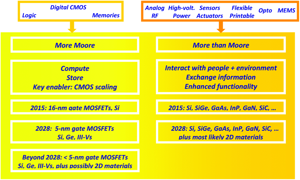 | ||
| Fig. 1 The More Moore and More Than Moore domains of semiconductor electronics, together with important trends and the semiconductors used in these domains. Note that the year 2028 indicates the end of the time horizon of the 2013 ITRS edition.7 | ||
More Moore encompasses digital ICs (integrated circuits) such as microprocessors and memories and covers around 70% of the overall chip market. Interestingly, today's digital ICs are based on one single semiconducting material, Si, one single transistor type, the Si MOSFET, and one single circuit technique, Si CMOS (complementary MOS) employing both n-channel (electrons constitute the transistor's output current) and p-channel MOSFETs (holes carry the current). For decades, chipmakers have introduced CMOS ICs with an exponentially increasing number of individual MOSFETs and, simultaneously, an exponentially decreasing price per transistor, to the market. Key to this evolution is the continuous shrinking of the MOSFET size, for short scaling. As shown in Fig. 2, since 2014, processors containing five billion MOSFETs with gate lengths around 20 nm have been commercially available and the introduction of a 10-billion processor has been announced for 2015.13 This trend of continuous device miniaturization and increasing circuit complexity is called Moore's Law.14
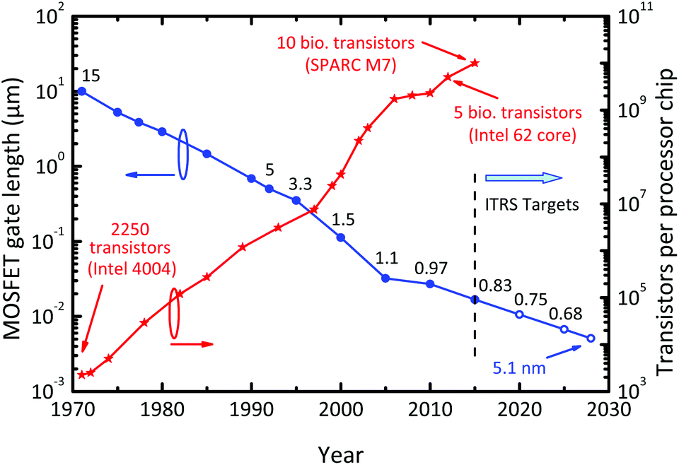 | ||
| Fig. 2 Evolution of the MOSFET gate length and the number of transistors integrated on a single microprocessor chip. The numbers above the gate length curve indicate the processor supply voltage VDD. Note the continuous decrease of VDD in the past and the required continuation of this trend in the future. The ITRS targets refer to MOSFETs for high-performance logic as specified in the 2013 ITRS edition.7 | ||
It is important to recognize that, to follow Moore's Law, increasing circuit complexity by scaling alone is not sufficient. Instead, the electrical performance of the scaled MOSFETs must be improved as well. In particular, transistor switching speed should increase exponentially and the energy needed for a single switching event should decrease exponentially. Only if these “triple dividends of MOSFET scaling”15 – smaller, faster, more power-efficient – can be achieved in concert, Moore's Law will survive.
In the recent past it has become more and more difficult to achieve the required performance improvements when scaling the Si MOSFET. A material property closely related to transistor performance is the carrier mobility, and a high mobility is always beneficial for transistor speed and power efficiency. Since Si, the backbone of today's More Moore circuits, offers only moderate mobilities, rigorous efforts are made to implement alternative high-mobility MOSFET channel materials into Si CMOS. A first step was the introduction of strain into the Si MOSFET channels leading to enhanced mobilities. Meanwhile, strained Si is widely used in CMOS production16 and research on high-mobility III–V and Ge channels for future MOSFET generations is aggressively pushed forward.15,17
Beyond the horizon of the current ITRS edition, when gate lengths below 5 nm will be required, MOSFETs with high-mobility (and thus light carrier effective mass) channels will encounter a fundamental problem. At this stage of scaling, the distance between the MOSFET's source and drain regions becomes so short that quantum-mechanical source–drain tunneling impedes proper FET operation. It may turn out that for sub-5 nm MOSFETs heavy effective mass materials with lower mobilities will become preferable since a heavy carrier effective mass suppresses source–drain tunneling.18,19
2.2 More Than Moore trends
More Than Moore is not primarily focused on increasing circuit complexity but rather on enhancing the functionality of ICs and electronic systems by combining digital electronics with components such as analog/RF (radio frequency) and high-voltage circuitry, sensors, actuators, etc. In the More Than Moore domain, traditionally the material basis has been much broader compared to More Moore and, apart from Si, a variety of alternative semiconductors is used to complement Si.More Than Moore covers a wide and heterogeneous field, see Fig. 1. Here we focus solely on RF electronics where at present, in addition to Si, the compound semiconductors based on GaAs, InP, and GaN are very popular. It should be noted that in RF electronics only n-channel FETs are used since in most materials electrons are faster than holes. A major trend in RF electronics is the striving for higher transistor operating frequencies and for extending transistor operation into the THz range. The evolution of the frequency performance of RF FETs in terms of the characteristic frequencies fT (cutoff frequency) and fmax (maximum frequency of oscillation) is shown in Fig. 3.
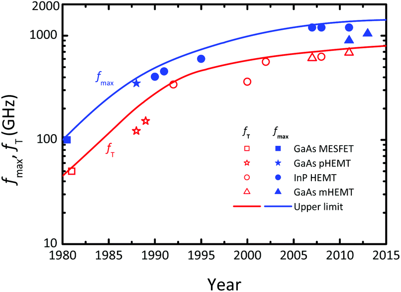 | ||
| Fig. 3 Evolution of the cutoff frequency fT and maximum frequency of oscillation fmax of RF FETs. Shown are the record fT and fmax values reported at a certain time. MESFET: metal-semiconductor FET; HEMT: high electron mobility transistor; pHEMT: pseudomorphic HEMT; mHEMT: metamorphic HEMT. Data are taken from ref. 20–39. | ||
As can be seen, the current record fmax of RF FETs is slightly above 1 THz, which means that FETs capable of THz amplification with reasonable power gain are still missing. On the other hand, the frequency range around and above 1 THz is attractive for applications in a variety of fields, such as security, medicine, and ultra-high-speed communications, to name just a few.40,41 Therefore, RF device engineers are looking for alternative FET channel materials offering improved mobility and closely follow the research on 2D materials.
2.3 Transistor figures of merit
A FET consists of a channel region connecting two reservoirs of mobile charges called source and drain. The third electrode (gate) is separated from the channel by a thin barrier. The applied gate–source voltage VGS controls the conductivity of the channel and the applied drain–source voltage VDS drives a drain current ID through the transistor. Fig. 4 shows a generic FET, together with the structures of Si MOSFETs, III–V HEMTs, and 2D MOSFETs. FETs are devices with the ability (i) to switch and (ii) to amplify signals and provide gain. For digital electronics, i.e., More Moore, switching is relevant while amplifying signals is important for RF applications.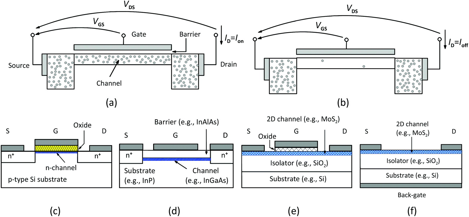 | ||
| Fig. 4 Basic FET structures. Generic structure of a FET (a) in the on-state and (b) in the off-state. (c) Conventional Si n-channel MOSFET. (d) HEMT. (e) 2D MOSFET. (f) Back-gate 2D MOSFET frequently used for proof-of-concept purposes. Note that HEMTs and 2D MOSFETs do not possess pn junctions as present in conventional Si MOSFETs shown in (c) but rather resemble the junctionless MOSFET which is intensively investigated at present.42 | ||
In digital logic, the FET is supposed to switch between on and off. In the on-state, see Fig. 4(a), the channel has a low resistance and a large on-current Ion can flow through it. As per definition, Ion is the transistor current for the bias condition VGS = VDS = VDD. In the off-state, see Fig. 4(b), on the other hand, the FET should block the current, the channel resistance should be high, and only a very small off-current Ioff is allowed to flow. The off-current is defined as the current flowing under the condition VGS = 0 and VDS = VDD. The gate voltage at which the transistor is just at the verge of switching on is the threshold voltage VTh. The transfer characteristics of a MOSFET shown in Fig. 5 indicate that in the subthreshold region (VGS < VTh) the drain current depends exponentially on VGS, followed by a transition region around VTh and finally by the superthreshold region where the drain current is essentially linearly dependent on VGS. As we have shown in Fig. 2, the supply voltage VDD of logic circuits has been decreased continuously over the years and a further reduction is required for the future. This means that logic transistors must switch from off to on within a very limited range of VGS.
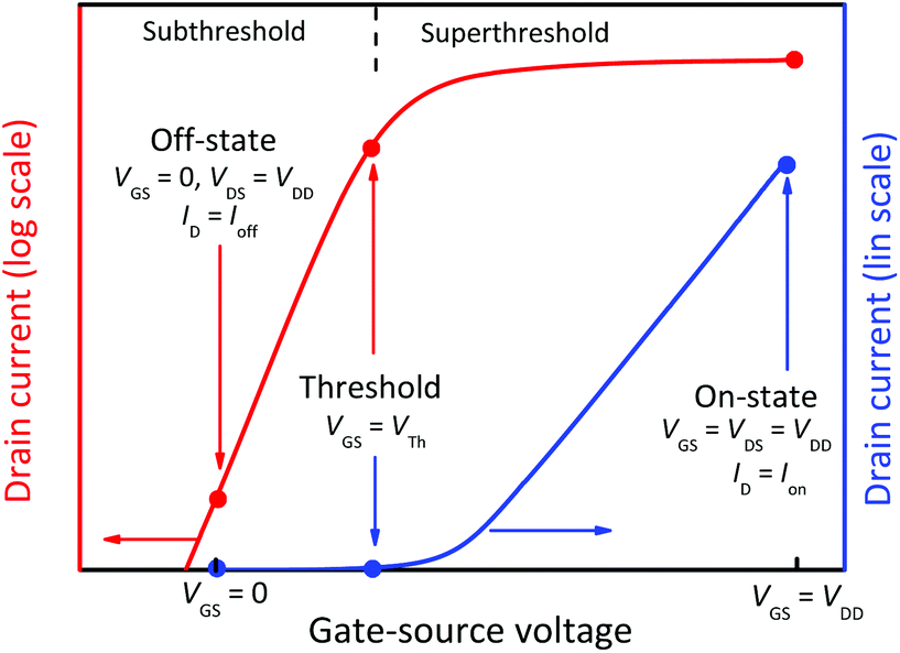 | ||
| Fig. 5 Transfer characteristics of an n-channel FET showing the drain current ID as a function of the gate-source voltage VGS together with the on and off operating points for CMOS logic. Note that the scale of the left current axis is logarithmic and that of the right current axis is linear. | ||
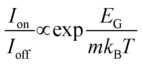
A further FOM (figure of merit) related to switching is the on–off ratio Ion/Ioff. For FETs to be used in digital logic, on–off ratios in the range of ≈104–5 × 10⁷ are required.7 As a basic rule, Ioff should be as low as possible and both Ion and the on–off ratio should be as high as possible. A low Ioff is needed for a low static power consumption of logic circuits while a high Ion is relevant for a high transistor switching speed.
When operated as an amplifier, on the other hand, the FET does not necessarily need to switch off. Instead, in most RF amplifier configurations the FET is permanently operated in the on-state and small signals applied to its input, i.e., the gate, appear amplified at the output. The extent to which the input signal is amplified is called gain. The small-signal current gain, for example, is defined as the RF output current of the transistor divided by the RF input current. Gains are frequency dependent and decrease with increasing frequency. Two important FOMs of RF transistors are the characteristic frequencies fT and fmax. The cutoff frequency fT is the frequency at which the small-signal current gain h21 of the transistor has dropped to unity (i.e., 0 dB) and the maximum frequency of oscillation fmax is the frequency where the unilateral power gain U becomes unity. It should be noted that for most RF applications, power gain and fmax are more important than current gain and fT. Moreover, as a rule of thumb, the operating frequency should be lower than 20% of the used transistors’ fmax to guarantee sufficient power gain. Fig. 6 shows the small-signal current and power gains of an RF FET as a function of frequency, together with fT and fmax.
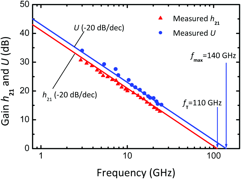 | ||
| Fig. 6 Small-signal current gain h21 and unilateral power gain U of a RF FET as a function of frequency, after ref. 43 and 44. The characteristic frequencies fT and fmax are obtained by extrapolating the measured h21 and U with the characteristic slope of −20 dB per dec. | ||
Commonly the voltage gain of RF FETs is not discussed explicitly since, if both current and power gain are reported, this data pair contains information on the voltage gain. Because FETs with gapless channels, e.g. graphene MOSFETs, suffer from poor power gain, an inspection of the voltage gain is advisable, however. The frequency-dependent voltage gain AV is defined as
| AV = z21/z11 | (1) |
| Gint = gm/gd | (2) |
All semiconductor devices generate fluctuations of voltage and current called noise. Noise is always undesirable and particularly critical for the amplification of small RF signals. A measure for the noise generated in a transistor is the noise figure NF, usually given in units of dB and defined as
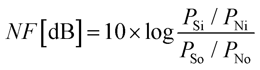 | (3) |
3. Overview of 2D materials
Inspired by the successful preparation of graphene, researchers have intensively examined options to obtain stable 2D materials beyond graphene. These efforts include real-world experiments where 2D materials have been prepared and analyzed, as well as computational experiments where the thermodynamic stability and the band structure of existing and hypothetical 2D materials have been computed. For the latter, particularly the Atlas of 2D Materials reporting the properties of more than 140 different 2D materials45 is worth mentioning.Recent experimental and theoretical efforts have shown that a variety of 2D materials beyond graphene does or should exist and that their electronic properties span the full range from metallic to insulating. Of particular interest for FET channels are the semiconducting and, to a lesser extent, the gapless semi-metallic 2D materials. Fig. 7 shows schematically the relevant parts of the band structure of different classes of these 2D materials.
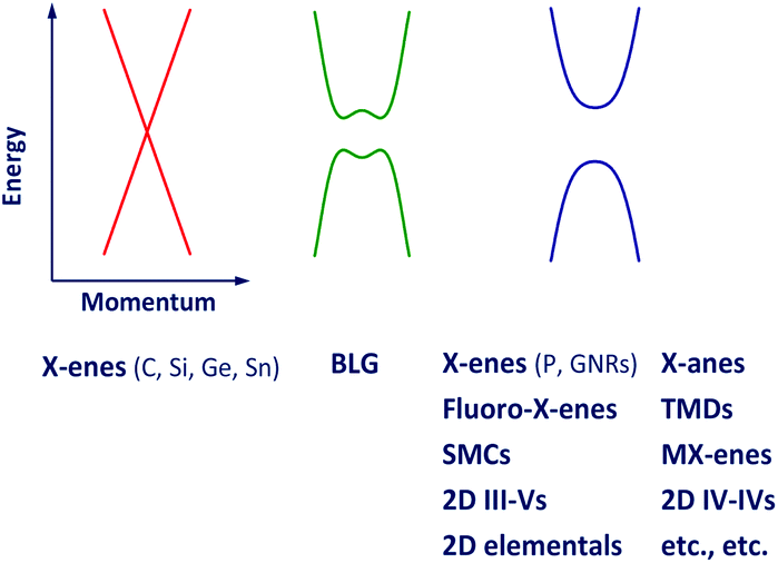 | ||
| Fig. 7 Schematic band structure of 2D materials relevant for transistors. BLG: bilayer graphene; GNR: graphene nanoribbon; TMD: transition metal dichalcogenide; SMC: semimetal chalcogenide. | ||
3.1 X-enes
Single-layer materials consisting of atoms of one single element arranged in a hexagonal lattice are designated as X-enes. So far, graphene as well as its Si-, Ge-, and P-based counterparts silicene,46 germanene,47 and phosphorene48 have been experimentally realized, and the band structure of stanene, the X-ene based on tin (Sn), has been calculated.49Compared to graphene, much less is known on the other X-enes. As of the end of 2014, the Web of Science database listed almost 91![[thin space (1/6-em)]](https://www.rsc.org/images/entities/char_2009.gif) 000 entries under the search term graphene compared to 654 entries for silicene, 133 for germanene, 81 for phosphorene, and 8 for stanene.50 As shown in Fig. 7, graphene, silicene, germanene, and stanene are gapless and have cone-shaped conduction and valence bands. The cones are frequently called Dirac cones and, correspondingly, graphene, silicene, germanene, and stanene are designated as Dirac materials. Phosphorene, on the other hand, is a semiconductor with a sizeable gap.
000 entries under the search term graphene compared to 654 entries for silicene, 133 for germanene, 81 for phosphorene, and 8 for stanene.50 As shown in Fig. 7, graphene, silicene, germanene, and stanene are gapless and have cone-shaped conduction and valence bands. The cones are frequently called Dirac cones and, correspondingly, graphene, silicene, germanene, and stanene are designated as Dirac materials. Phosphorene, on the other hand, is a semiconductor with a sizeable gap.
3.2 X-anes
The crystallographic structure of the X-anes is closely related to that of the X-enes. They also possess a hexagonal lattice of carbon (graphane), silicon (silicane), germanium (germanane), or tin (stanane) atoms. However, their lattice atoms are additionally out of plane bonded to hydrogen atoms – this is frequently called hydrogenated. Graphane was predicted to exist in 200751 and was produced experimentally shortly afterwards.52 Recently, germanane could also be realized experimentally.53 Most relevant for electronic applications is the fact that graphane, silicane, and germanane possess sizeable bandgaps.3.3 Fluoro-X-enes
The structure of these materials is very similar to that of the X-anes. Here, the lattice atoms are bonded out of plane to F (fluorine) atoms. Fluorographene has already been produced experimentally and shown to have a wide gap of around, possibly even exceeding, 3 eV.54,55 Theory has confirmed these results for fluorographene and predicted a gap around 1 eV for fluorosilicene while fluorogermanene seems to be gapless.453.4 TMDs
The TMDs constitute a group of materials consisting of a transition metal M (elements of groups 4, 5, and 6 of the periodic table of elements) and a chalcogen Q, i.e., sulfur (S), selenium (Se), or tellurium (Te). These M and Q elements form covalently bonded 2D layers of the MQ2 type (e.g., MoS2) with a hexagonal lattice. Single-layer TMDs consist of three atomic layers where a layer of M atoms is sandwiched between two layers of Q atoms. For example, single-layer MoS2 is composed of one layer of molybdenum atoms and two layers of sulfur atoms. Today, more than 40 different types of TMDs are known.10 While many of them are metallic, those containing Mo and W (i.e., MoS2, WSe2, etc.) as well as several of the Hf-, Pd-, Pt-, and Zr-based TMDs are semiconductors with bandgaps of the order of 1–2 eV.10,45 It should be noted that TMDs occur in different polytypes 1T, 1T’, 2H, and 3R, where T means trigonal, T’ distorted trigonal, H hexagonal, and R rhombohedral, and 1, 2, or 3 indicates the number of TMD layers in the unit cell,56,57 which have different properties. For example, the common 2H polytypes of the Mo- and W-based TMDs are semiconducting while their metastable counterparts of the 1T type are metallic.583.5 SMCs
SMCs consist of a semimetal M (Ga or In) and a chalcogen (S or Se). In contrast to the TMDs, they are expected to occur in M2X2 stoichiometry in a four-layer X–M–M–X configuration and to be semiconducting.453.6 MX-enes
There is a material class called the MAX phase family comprising more than 60 individual ternary layered materials.59 These materials have a hexagonal lattice and the composition Mn+1AXn where M is an early transition metal, A is a group 13 or 14 element, X is either carbon or nitrogen, and n is an integer equal to 1, 2, or 3. The bonds between the M and X atoms are much stronger than the M–A bonds so that the A atoms can easily be removed, e.g., by an acid treatment. By a subsequent sonication, single Mn+1Xn layers, the so-called MX-enes, can be obtained. As the first MX-ene, Ti3C2 has been successfully prepared from the MAX material Ti3AlC2,60 soon followed by the experimental verification of five further MX-enes,61 and the existence of even more MX-enes has been predicted. Furthermore, F2, (OH)2, and O2 groups can be attached to the pure MX-enes of the M2X configuration, resulting in the formation of the modified MX-enes M2XF2, M2X(OH)2, and MXO2.62 Several modified MX-enes have been predicted to be semiconductors with sizeable bandgaps.623.7 Further 2D materials
By first-principles calculations, the phonon properties and band structures of entire classes of 2D IV–IV and III–V compounds and of many other 2D materials have been investigated. It has been shown that a large body of these 2D materials with both hexagonal and tetragonal lattice structures should be stable and show bandgaps between 0.2 and 5 eV.45,63,64 Although it is uncertain whether all these 2D materials can be synthesized, at least part of them may become available for experiments in the future.3.8 Production of 2D materials
To fabricate 2D transistors, first the 2D starting material must be produced, preferably in the form of large-area sheets with uniform thickness and high crystallographic quality. Layered van der Waals materials, where the stacked layers are bound by weak van der Waals forces, can be exfoliated. Mechanical exfoliation is widely used to produce graphene,1 TMDs,6 and phosphorene48 layers. While this approach is simple and does not require expensive equipment, it is time consuming and provides flakes of limited size only. Liquid exfoliation as a second exfoliation method delivers 2D flakes dispersed in a liquid.65 This method is very effective, but the dispersed flakes are small, which makes transistor and circuit processing challenging.As an alternative, wafer-scale 2D materials can be grown on substrates. Epitaxial graphene on SiC has successfully been formed and used for transistor processing.66 Graphene can also be grown by CVD (chemical vapor deposition) on metals and subsequently be transferred to insulating substrates such as oxidized Si wafers.67 Furthermore, different TMDs such as MoS2, WS2, and WSe2 have been grown by CVD directly on oxidized Si wafers.68,69 Finally, silicene has been grown on metals and transferred to SiO2/Si substrates for device processing.70
4. Properties of 2D materials relevant for transistors
4.1 The ideal material for a FET channel – a wish list†
To assess the potential of novel materials for FET channels it is not sufficient to consider only one single material property such as the carrier mobility. Instead, a set of properties should be examined to get a realistic impression on the suitability of the new material for transistors. Therefore, in the following we compose a (certainly not complete) wish list for the material properties of a FET channel, particularly for use in digital logic and RF FETs, and examine the extent to which the 2D materials meet our wishes. In the discussion it should always be kept in mind that research on most of the 2D materials has just begun and is in an embryonic stage compared to the conventional 3D bulk semiconductors such as Si, Ge, and the III–V compounds. This leads to the situation that, while our wish list itself is well established and relies on the experiences of decades of transistor research, the available data for the relevant properties of the 2D materials are rather fragmentary.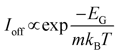 | (4) |
 | (5) |
Estimations suggest that at room temperature a gap of the order of 400 meV is needed to achieve a sufficiently good switch-off and the required on–off ratios.72–74
Since RF FETs can permanently be operated in the on-state and do not need to switch off, one might conclude that here a gap is not needed. Unfortunately, the situation is more complex. It has been discussed in detail that to achieve a high power gain and high fmax, the FET needs to show a sufficiently good saturation of the drain current and for that, in turn, a gap is needed.3 Current gain and fT, on the other hand, are less affected by a missing or weak current saturation. Thus, transistors with gapless channels can provide high current gain and fT but suffer from poor power gain and fmax. It is not exactly known how wide the gap of the channel of a good RF FET should be. Most likely, the requirements are less stringent than for logic FETs. The fastest and least noisy RF FETs are InP HEMTs32 and GaAs mHEMTs75,76 having InxGa1−xAs channels with high In contents x ranging from 0.7 (EG ≈ 0.65 eV) to 1 (i.e., InAs, EG = 0.35 eV). Experiments with InSb channel HEMTs (EG InSb = 0.17 eV), on the other hand, revealed that these transistors, despite being fast, show lower fT and fmax compared to InP HEMTs and GaAs mHEMTs with a similar gate length.77,78 This suggests that the 0.17 eV gap of InSb might already be too narrow for ultra-high-performance RF FETs.
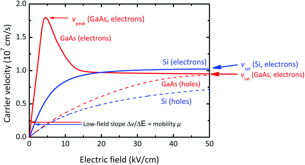 | ||
| Fig. 8 Velocity-field characteristics for electrons and holes in Si and GaAs. Note the peak of the electron velocity in GaAs and the soft saturation of the other v–E characteristics. | ||
For logic FETs, a high mobility and a high saturation velocity are always desirable. It should be mentioned, however, that Si MOSFETs show surprisingly good switching characteristics in spite of the rather moderate μ (200–500 cm2 V−1 s−1) and vsat (107 cm s−1). The InxGa1−xAs channels of the best RF FETs, i.e., InP HEMTs and GaAs mHEMTs, show mobilities of 10000–15000 cm2 V−1 s−1 and peak velocities of 3–4 × 107 cm s−1, and alternative channel materials that are to compete with InxGa1−xAs for high-performance RF FETs should show at least similar transport characteristics, combined with an appropriate bandgap. Reasonably good RF performance, however, can be achieved already with lower mobility channels, e.g., Si channels of RF Si MOSFETs, provided the contact resistance (see entry #4) is low and the scale length (entry #5) is short.
The thermal conductivity of the channel material, however, does not tell the whole story of heat transport, in particular if the transistor is located on a substrate different from the channel material. 2D FETs, such as graphene or TMD FETs (see Fig. 4e showing a MoS2 MOSFET), are frequently realized on the surface of oxidized Si wafers. Here, the heat generated in the channel first has to cross the channel–SiO2 interface acting as a thermal boundary resistance RTB, move through the SiO2 layer, and then cross the SiO2–substrate interface forming a second RTB before it can spread across the Si substrate.79 To limit self-heating, the thermal conductivity of the FET channel material and of all materials underneath should be high and the thermal boundary resistances of all interfaces between the channel and the back side of the chip should be low.
Due to the voltage drop across RS, part of the applied VGS is lost for the control of the current as can be seen from
| VGS = VGS-int + ID(Rco-S + Rser-S) = VGS-int + IDRS | (6) |
Similarly, the applied drain–source voltage VDS is different from the intrinsic drain–source voltage VDS-int according to
| VDS = VDS-int + ID(RS + RD) | (7) |
The parasitic source and drain resistances RS and RD, and thus the contact resistance Rco, deteriorate transistor performance. Therefore, the Rco should be as low as possible.
The contact resistance is proportional to the inverse of the contact width, i.e., Rco ∝ 1/W. To compare the contact resistances obtained from structures with different contact widths, Rco is commonly normalized with respect to the contact width and is given in units of Ω mm.
 | (8) |
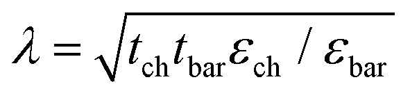
| L ≥ a × λ | (9) |
Three issues related to the scale length should be borne in mind. First, eqn (8) has been derived for fully depleted SOI (silicon on insulator) MOSFETs with relatively thick Si channels. Thus, strictly speaking, eqn (8) does not apply to FETs with extremely thin channels, e.g. channels of 2D materials. Second, the effect of the insulating layer underneath the channel has not been taken into account. Third, the scale length concept is valid only for semiconducting channels and does not apply to gapless channels. The main message of eqn (8) and (9) is that a thin channel region is beneficial for suppressing short-channel effects and FET scaling. If not only the trend is of interest, but actual numbers for the scale length of MOSFETs with 2D channels are needed, more elaborate scale length expression developed for atomically thin channels should be used.81,82
 | (10) |
Second, beyond the horizon of the 2013 ITRS edition, when gate lengths of 5 nm and below will be needed and source-to-drain tunneling will become an issue, FETs with high-mobility light-meff channels may fail and channel materials with wider bandgap, heavier carrier effective mass (and, consequently, lower mobility) may be preferred to suppress source-to-drain tunneling.18,19
Table 1 summarizes our discussion on the wish list for the properties of FET channel materials.
| Entry # | Property | Desirable |
|---|---|---|
| 1 | Bandgap | Logic: ≥0.4 eV |
| hp RF: sizeable, probably lower limit below 0.4 eV and optimum above 0.17 eV | ||
| 2 | Carrier transport | |
| Carrier effective mass | Logic: light (L > 5 nm), meff < 0.1 | |
| heavy (L ≤ 5 nm), meff ≥ 0.5 | ||
| hp RF: very light, meff < 0.05 | ||
| Mobility | hp Logic: high, > 500 cm2 V−1 s−1 | |
| hp RF: very high, > 10000 cm2 V−1 s−1 |
||
| Peak/saturation velocity | Logic: high, >107 cm s−1 | |
| hp RF: very high, ≥3 × 107 cm s−1 | ||
| 3 | Heat transport | |
| Thermal conductivity | High | |
| Thermal boundary resistance | Low | |
| 4 | Contact resistance | Low, ≤0.03 Ω mm |
| 5 | Scale length, channel thickness | Small |
Good carrier transport properties, most notably a high mobility, are important for a high on-current and a high fT, while bandgap and scale length are most relevant for the off-current and, to a certain extent, for drain current saturation and fmax.
4.2 Bandgap of 2D materials
The bandgap information for 2D materials available in the literature comprises a limited amount of measured data and a wide body of results obtained from first-principle (ab initio) calculations. Calculations provide not only the bandgap itself, but the entire band structure, from which the carrier effective masses can be extracted. Thus, first-principle calculations are a very useful means of assessing the suitability of a semiconductor for FET channels. It should be mentioned, however, that different methods of first-principle calculations can lead to quite different bandgaps for one and the same material. The popular DFT (density functional theory) systematically underestimates the bandgap, while computationally more demanding approaches, such as GW, predict wider gaps which, however, in some cases exceed the measured gaps.45,84Two examples for the considerable differences between the bandgaps obtained from DFT calculations and those calculated using more rigorous methods are given below. For germanane, the bandgap predicted by DFT ranges from 0.95 eV85 to 1.53 eV53 compared to values in the range of 1.84 eV45 to 3.6 eV86 obtained by other methods and a measured gap of 1.59 eV.53 As a second example we consider GNRs. For N = 7 armchair GNRs (N is the number of carbon atoms along the GNR width and N = 7 corresponds to a width of about 0.74 nm), a gap of 3.8 eV has been calculated by the GW method87 compared to 1.5–1.6 eV obtained by DFT87,88 and measured gaps of 2.3–2.8 eV.89,90 Thus, calculated bandgaps should be treated as estimates rather than accurate predictions, and those obtained by DFT calculations as a lower limit. On the other hand, the shape of the individual bands calculated by DFT and the extracted carrier effective masses can be considered as reasonable guides.45
Large-area graphene is gapless and the same holds for silicene and germanene.45 There are, however, options to open a gap in these materials. For graphene, the first approach is to form narrow GNRs by either chemical synthesis91,92 or lithographic patterning.93,94 Chemically synthesized GNRs with atomically precise edges have been reported while patterned GNRs typically show non-ideal edges that degrade carrier transport. Fig. 9 compiles theoretical bandgap data (calculated by the GW method) together with experimental bandgap data for GNRs and shows the general trend of an increasing gap for decreasing width. As can be seen, narrow ribbons having a width of 10 nm or less are needed to achieve the 0.4 eV gap required for digital logic.
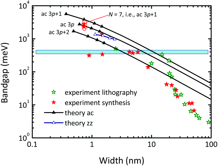 | ||
| Fig. 9 Bandgap of GNRs vs. ribbon width. Shown are theoretical data obtained by the GW method for ac (armchair) GNRs of the 3p, 3p + 1, and 3p + 2 families (full triangles and lines, p is an integer) and for zz (zigzag) GNRs from ref. 87, together with measured results for chemically synthesized89,90,95 and lithographically patterned93,94 GNRs. | ||
The second option to open a gap in graphene is by applying a perpendicular electric field to BLG, i.e., two graphene layers, one located directly on top of the other.96,97 As shown in Fig. 7, the conduction and valence bands of biased BLG are not parabolic as for most other semiconductors, but Mexican-hat-shaped.96 For FET-relevant BLG structures, realistically gaps up to 130 meV can be expected.97 This might be helpful for RF FETs but is not sufficient for digital logic FETs.
Recent calculations have predicted a gap opening in silicene and germanene nanoribbons98 as well as in single-layer silicene and germanene when a vertical electric field is applied.99 For a given field, however, the gap in silicene and germanene is smaller than that in biased BLG. Thus, regarding the bandgap, large-area silicene and germanene are not suited for logic FETs and their potential for RF FETs is unclear.
The bandgaps of the 2D materials (except Dirac materials, nanoribbons, BLG, and biased silicene and germanene) are summarized in Fig. 10. To guarantee consistency, all gaps shown are calculated by DFT. True semiconductors (EG = 0.5–2 eV) are phosphorene, germanane, fluorosilicene, the Mo- and W-based TMDs, as well as HfS2, ZrS2, and TiS2, GaSe, InSe, and several MX-enes. Graphane, silicane, fluorographene, GaS, InS, and SiC can be considered as wide bandgap semiconductors while BN is an insulator. For comparison, bandgap data for conventional 3D semiconductors widely used for FET channels are also shown in Fig. 10.
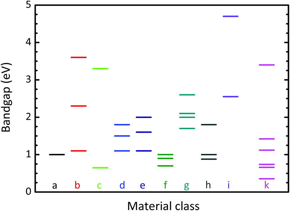 | ||
| Fig. 10 Bandgap of semiconducting and insulating 2D materials calculated by DFT (data taken from ref. 45 unless otherwise stated). The letters indicate the material class. (a) Semiconducting X-enes (phosphorene,100 note that graphene, silicene, and germanene are gapless). (b) X-anes (from top to bottom graphane, silicane, germanane). (c) Fluoro-X-enes (fluorographene, fluorosilicene, note that fluorogermanene is gapless). (d) Mo-based TMDs (MoS2, MoSe2, MoTe2). (e) W-based TMDs (WS2, WSe2, WTe2). (f) Further disulfides (HfS2, ZrS2, TiS2). (g) SMCs (GaS, InS, GaSe, InSe). (h) MX-enes62,101 (top: Sc2CO2, middle: Hf2CO2, Sc2CF2, Ti2CO2 (all 1 eV), bottom: Zr2CO2). (i) BN, SiC. Also shown are the gaps of conventional 3D semiconductors labeled as material class k (GaN, GaAs, Si, In0.53Ga0.47As, Ge, InAs). | ||
Due to its wide gap, BN is not really a candidate channel material. It has, however, successfully been used as a gate dielectric for graphene MOSFETs102 and moreover shown to have a beneficial effect on the mobility in graphene channels underneath or above it.102,103
The bandgap of TMDs and phosphorene depends on the layer number. It is widest for single layers and gradually decreases with increasing layer number toward the bulk value. This is important since the channels of experimental TMD and phosphorene MOSFETs frequently consist of few-layer material instead of single layers. The thickness dependence of the gap is particularly pronounced for phosphorene where the gap decreases from 1 eV for single layers (see Fig. 10) down to 0.67 and 0.52 eV for bilayer and trilayer materials.100
In summary we state that in terms of bandgap many 2D materials fulfill the requirements of our wish list and therefore are suitable for FET channels.
4.3 Carrier transport and effective mass
It is well established that the carrier mobility of semiconductors tends to decrease with increasing bandgap. From Fig. 11 showing this trend for the electron mobility μn, we see that for the III–V compounds (black full circles), the electron mobility reduces from 77000 cm2 V−1 s−1 for the narrow-bandgap InSb to 3000 cm2 V−1 s−1 for the wider-bandgap Ga0.51In0.49P (EG = 1.85 eV). Si (EG = 1.12 eV) and Ge (EG = 0.66 eV) follow this tendency although for these materials the electron mobility is lower than that of the III–V compounds with a comparable gap. Also graphene cannot escape from this mobility-bandgap trend. Suspended gapless graphene shows very high electron mobilities of up to 200000 cm2 V−1 s−1. The electron mobility in gapless graphene on insulating substrates is lower, but still impressively high as shown in Table 2. The gap opening in GNRs and biased BLG results, however, in a dramatic mobility reduction.
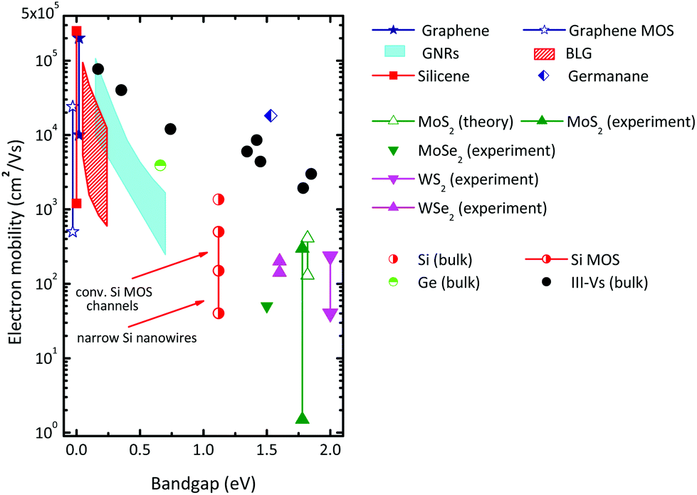 | ||
| Fig. 11 Room-temperature electron mobility vs. bandgap for different materials. The data for the conventional 3D bulk semiconductors taken from the compilation in ref. 44 relate to undoped material. III–V materials (black solid circles), from left to right InSb, InAs, In0.53Ga0.47As, InP, GaAs, In0.52Al0.48As, Al0.3Ga0.7As, Ga0.51In0.49P. Experimental data for graphene and simulated mobilities for GNRs and BLG taken from the compilation in ref. 3. Calculated mobilities for silicene and germanene taken from ref. 104–106. Simulated MoS2 mobilities taken from ref. 104, 107 and 108, experimental MoS2 data taken exemplarily from ref. 6 and 109–112, and those for WS2, MoSe2 and WSe2 from ref. 113, 114, 124 and 125. | ||
000 cm2 V−1 s−1 (ref. 120)
The electron mobility data reported by early 2015 for 2D materials beyond graphene are also included in Fig. 11. For MoS2, phonon limited mobilities, i.e., the upper mobility limit for defect-free undoped material, ranging from 130 cm2 V−1 s−1 (ref. 104) to 410 cm2 V−1 s−1 (ref. 107), have been calculated and mobilities between 1 and 300 cm2 V−1 s−1 have been extracted from experimental MoS2 MOSFET structures, see, e.g., ref. 6, 109–112. Note that (i) the mobility reported for back-gated MoS2 MOSFETs (a few to a few tens of cm2 V−1 s−1) is lower than the mobility observed in top-gated MoS2 FETs (several tens to a few hundreds of cm2 V−1 s−1), and (ii) for top-gated MoS2 FETs occasionally electron mobilities of up to 1000 cm2 V−1 s−1 (ref. 121) have been reported. These data are not included in Fig. 11 since it most likely results from an irregular extraction approach.122,123
For single-layer WSe2, a hole mobility of 250 cm2 V−1 s−1 has been reported126 that compares favorably with the best electron mobilities around 200 cm2 V−1 s−1 observed in multi-layer WSe2114 and in ref. 127 it has been shown that the hole mobility in WSe2 can indeed be higher than the electron mobility. In few-layer phosphorene, a remarkable hole mobility of 1000 cm2 V−1 s−1 has been measured.128
Velocity-field characteristics for gapless graphene have been simulated and measured, and for BLG, GNRs, silicene, and MoS2 high-field transport data have been simulated. The reported v–E characteristics of 2D materials show a soft saturation with a slight decline of the velocity at high fields. Table 3 summarizes the available saturation and peak velocity data for 2D materials. These high-field transport data can be compared with the v–E characteristics for Si and GaAs in Fig. 8.
| Material | v peak (107 cm s−1) | v sat (107 cm s−1) | Comment | Ref. |
|---|---|---|---|---|
| Graphene | — | 1–3 @ 20 | Exp. + fit, different nS | 129 |
| Graphene | 5.8 @ 15 | 5.2 @ 50 | Sim., nS = 1011 cm−2 | 130 |
| BLG | 3.4 @ 5 | 2.9 @ 20 | Sim., nS = 5 × 1011 cm−2 | 131 |
| BLG | — | 3.0 @ 25 | Sim., nS = 1012 cm−2, EG = 0.1 eV | 130 |
| GNR | 3.7 @ 10 | <3 @ >30 | Sim., nS = 1012 cm−2, w = 10.1 nm | 132 |
| >3.1 @ >100 | — | Sim., nS = 1012 cm−2, w = 2.62 nm | ||
| GNR | — | 3.3 @ 25 | Sim., nS = 1012 cm−2, EG = 0.4 eV | 130 |
| Silicene | 0.5 @ 30 | 0.46 @ 50 | Sim. | 104 |
| 0.39 @ 100 | ||||
| MoS2 | — | 0.34 @ 100 | Sim. | 104 |
| MoS2 | — | 1.5 @ 100 | Sim. | 108 |
It should be mentioned that for future generations of Si-based logic ICs, ultra-thin-body SOI MOSFETs and possibly Si nanowire MOSFETs with ultra-small body cross-section will be needed and that in these structures, the mobility is degraded and much smaller compared to bulk Si. For example, in sub-5 nm diameter Si nanowire MOS structures, the electron mobility at low perpendicular effective fields can be below 100 cm2 V−1 s−1 and drop further at higher effective fields down to a few tens of cm2 V−1 s−1.133,134 Thus, several 2D semiconductors can be considered as a viable alternative.
If carrier transport data for a new material are not available, an examination of the material's band structure and carrier effective mass can be helpful. Although the effective mass is not the only quantity influencing the mobility, a light effective mass is always an indication for a high mobility. In Fig. 12 the electron effective mass of 2D materials and of conventional semiconductors is plotted as a function of the bandgap.
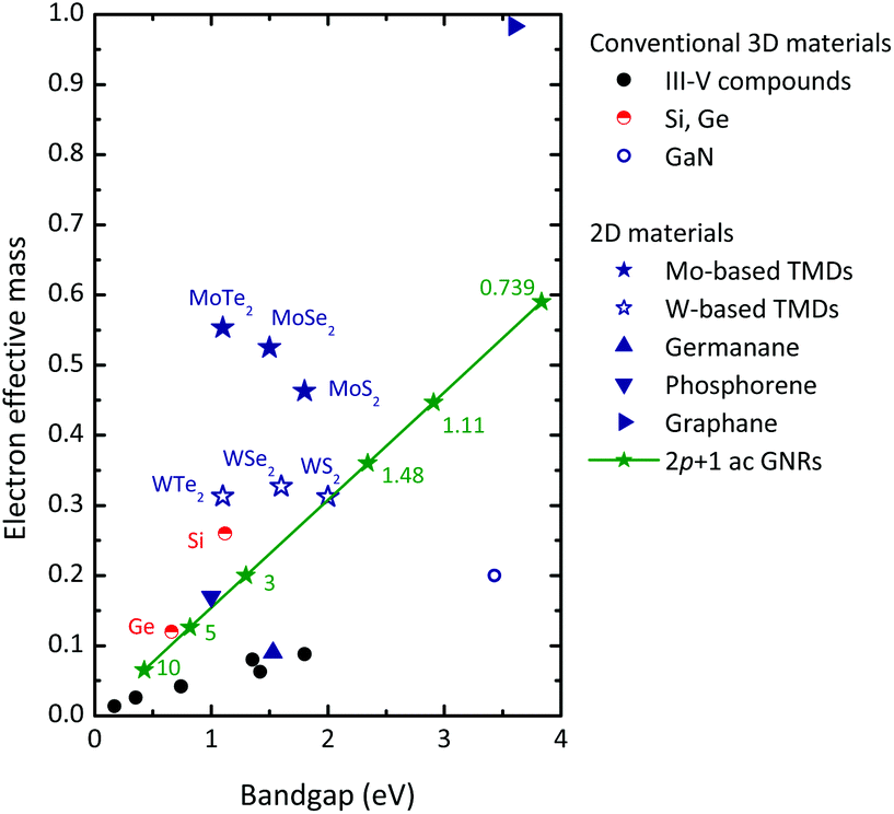 | ||
| Fig. 12 Electron effective mass of 2D and conventional 3D semiconductors vs. bandgap. III–V compounds (black solid circles), from left to right InSb, InAs, In0.53Ga0.47As, InP, GaAs, Al0.3Ga0.7As. Data for TMDs and graphane from ref. 45, for germanane from ref. 53, for GNRs from ref. 135, and for phosphorene from ref. 136 and 137. The numbers at the GNR data points indicate the ribbon width according to the width–gap relationship from ref. 87. | ||
For conventional semiconductors (Si, Ge, III–V compounds) the hole mobility μp is always lower than the electron mobility. This is particularly true for the III–V compounds with very high electron mobility. The ratio μp/μn is around 0.5 for Ge, 0.3 for Si, 0.05 for GaAs, and approaches 0.01 for the narrow bandgap compounds InAs and InSb. For the Mo- and W-based TMDs45 and for germanane,53 as well as for phosphorene for transport in the armchair direction,100,136,137meff-n/meff-p ratios (meff-n and meff-p are the electron and hole effective masses) of 0.8–1 have been calculated and band structure calculations for BLG and GNRs also reveal a high degree of symmetry of the top of the valence band and the bottom of the conduction band. This suggests μp/μn ratios close to unity for these materials. For CMOS logic, μn ≈ μp is highly desirable since under these conditions a symmetric design of n- and p-channel MOSFETs is possible.
When comparing the electron mobilities of the 2D materials in Fig. 11 with those of the conventional 3D semiconductors it seems that the semiconducting 2D materials show rather moderate mobilities and, with the exception of germanene, do not compete well. This leads us to the conclusion that the 2D materials cannot compete with the high-mobility III–V compounds and will not be suitable for ultra-fast high-performance transistors. On the other hand, their mobilities are appropriate for many other applications where high speed is not of primary importance. The calculated electron mobility of more than 18000 cm2 V−1 s−1 for germanane,106 on the other hand, is very promising. However, this result needs to be confirmed by experiments and to be reproduced by calculations of other groups.
4.4 Heat transport
Table 4 summarizes the currently available data for the thermal conductivity of 2D materials in comparison with that of 3D bulk materials. The thermal conductivity of suspended graphene exceeds that of metals (e.g., κCu = 400 W m−1 K−1) and the maximum reported record value from ref. 138 is even above that of bulk graphite. The thermal conductivity of graphene on SiO2 is still high but lower compared to suspended graphene due to interface interactions. GNRs as well as the Mo- and W-based TMDs show lower thermal conductivities.| 3D bulk materials | 2D materials | |||||
|---|---|---|---|---|---|---|
| κ | Ref. | Substrate | κ | Ref. | ||
| Si | 130 | 44 | Graphene | SiO2 | e, 600 | 141 |
| SiC | 290 | 44 | GNR | SiO2 | e, 80 | 142 |
| SiO2 | 1.5 | 44 | MoS2 | No substrate | e, 34 | 143 |
| Graphite | 2000 | 139 | MoS2 | No substrate | s, 103 | 144 |
| MoS2 | 2.4 | 140 | MoSe2 | No substrate | s, 54 | 144 |
| WS2 | 1.9 | 140 | WS2 | No substrate | s, 142 | 144 |
| WSe2 | 1.2 | 140 | WSe2 | No substrate | s, 53 | 144 |
Table 5 shows the thermal boundary resistance RTB of graphene/SiO2, graphene/SiC, and graphene/BN junctions and for comparison that of silicon on SiO2 as used in modern SOI structures. Unfortunately, information on the thermal boundary resistance for the 2D materials beyond graphene is not yet available. The measured RTB of single-layer graphene on SiO2145,146 is more than a factor of 10 larger than that calculated for Si on SiO2.147,148 This factor of 10, however, is less critical than it seems on first sight. Usually the thermal resistance encountered by the heat flow from the chip surface (where the devices are located and the heat is generated) to the heat sink at the back side of the chip is much larger than the thermal boundary resistance the heat has to surmount when flowing from the 2D channel to the underlying substrate. To illustrate this issue, let us consider a graphene device layer located on a Si wafer (thickness tSi = 360 μm) covered with SiO2 (thickness tSiO2 = 90 nm) and assume the simplified case of a homogeneous heat flow from the graphene layer downward to the bottom of the substrate. The heat generated in the graphene layer first crosses the graphene/SiO2 interface having a thermal boundary resistance RTB1, flows through the SiO2 layer with a thermal resistance Rth-ox, then crosses the SiO2/Si interface (RTB2), and finally flows through the Si substrate (Rth-Si).
The overall thermal resistance is the sum of the individual contributions152 and reads as
 | (11) |
Note that the heat transport parameters from Tables 4 and 5 relate to room temperature. When the temperature rises beyond room temperature, the thermal conductance decreases (undesirable) and the thermal boundary resistance decreases (desirable) as well.149,153
Reliable targets for the thermal conductivity and the thermal boundary resistance of FET channel materials have not yet been established. It is certainly fair, however, to state that both κ and RTB of the 2D materials should not fall far behind those of Si and the III–V compounds.
4.5 Contact resistance
The first contact experiments for 2D materials have been focused on graphene and revealed that achieving low-resistance contacts is challenging. In late 2010, the best metal–graphene contact resistances have been in the range 0.5–10 Ω mm,154i.e., orders of magnitude higher than for contacts to Si and III–V compounds. Therefore, a lot of effort has been invested in reducing the metal–graphene contact resistance that finally led to significant improvements. Today, metal–graphene contact resistances as low as 0.01–0.2 Ω mm have been achieved. This already comes close to the resistance of state-of-the-art metal contacts on Si and III–V semiconductors.Meanwhile, data for metal–TMD and metal–phosphorene contacts have been reported as well. Here, however, the contact resistance is still too high and typically exceeds 0.5 Ω mm. Table 6 summarizes the state-of-the-art metal contacts on 2D materials and on conventional semiconductors.
| Transistor type | R co (Ω mm) | Metal | Comment | Ref. |
|---|---|---|---|---|
| Graphene MOSFET | 0.011–0.08 | Ni, Ti | BL | 155 and 156 |
| 0.1–0.2 | Ti, Ni, Pd/Au, Cr/Au | SL | 155–158 | |
| MoS2 MOSFET | 0.2–1.6 | Ni/Au, Ti/Au, Au | FL | 159–162 |
| 2 | Au | SL | 163 | |
| WSe2 MOSFET | 1.4 | Graphene | BL | 164 |
| 2 | Graphene | FL | 165 | |
| Phosphorene MOSFET | 1.75 | Ni/Au, PdAu | FL | 166 |
| Si MOSFET | <0.01 | 167 | ||
| InP HEMT | 0.03 | 168 | ||
| GaAs mHEMT | 0.02 | 169 |
From the ITRS one can get an impression about the contact requirements related to logic MOSFETs. During the entire horizon of the 2013 ITRS edition, the maximum allowed parasitic resistance (which includes both the contact resistance itself and the semiconductor series resistance, see eqn (4)) is around 0.065 Ω mm. Thus, the contact resistance must be significantly below 0.065 Ω mm. As Table 6 indicates, so far only graphene has fulfilled this requirement. Given the successful reduction of Rco for metal–graphene contacts by more than an order of magnitude within a few years, we expect sizeable improvements for TMD and phosphorene contacts in the near future as well.
4.6 Scale length
Table 7 shows the scale length λ of GNR, MoS2, and Si MOSFETs as well as of InP HEMTs and GaAs mHEMTs obtained using eqn (8). The results indicate that, in terms of scale length and thus regarding the suppression of short-channel effects and scaling limits, the FETs with 2D channels behave much better than those with conventional channel materials.| Transistor class | ε r-ch | ε r-bar | t ch (nm) | t bar (nm) | λ (nm) |
|---|---|---|---|---|---|
| Si SOI MOSFET | 11.9 | 3.9 | 5 | 0.6 | 3 |
| InP HEMT & GaAs mHEMT | 14.1 | 12.7 | 15 | 15 | 16 |
| GNR MOSFET | 1.8 | 3.9 | 0.35 | 0.6 | <1 |
| MoS2 MOSFET | 2.8 | 3.9 | 0.72 | 0.6 | <1 |
5. State-of-the-art 2D FETs
In the following, the status of research on 2D transistors is reviewed by presenting experimental transistor data collected from the literature. In addition, transistor performance trends are discussed on the basis of theoretical considerations.5.1 X-ene FETs
To circumvent the problems of gapless large-area graphene, vertical non-FET transistor concepts that do not require a gap for switch-off have been elaborated. These concepts rely either on graphene–Si Schottky barriers as described in ref. 174, where on–off ratios of up to 105 have been demonstrated, on tunneling through an insulator between two graphene layers,175 or on using graphene as the base of a hot electron transistor.176 These devices represent interesting options to exploit gapless graphene in logic transistors and can in general be realized also using 2D materials beyond graphene. It is difficult, however, to assess their true potential for future logic at the moment.
In terms of fT, graphene MOSFETs perform competitively. They outperform Si MOSFETs with comparable size and compete well with InP HEMTs and GaAs mHEMTs (which are the fastest RF FETs of all) down to gate lengths of about 60 nm.3 Regarding the more important FOM fmax, however, the picture looks less promising for graphene MOSFETs. While the record fmax of InP HEMTs and GaAs mHEMTs exceeds 1 THz and Si MOSFETs with an fmax of 420 GHz have been reported, the best graphene RF FETs show an fmax of about 100 GHz only.182 It has been discussed in detail that the main reason for this poor fmax performance is the missing gap in large-area graphene.3 Thus, no matter how carefully the design of large-area graphene FETs is optimized, these transistors will never compete well with III–V HEMTs and Si MOSFETs in terms of power gain and fmax.
When comparing experimental fT and fmax data of graphene MOSFETs with that of other RF FETs, one should take a closer look at the applied de-embedding procedure. De-embedding is a common practice in RF electronics to eliminate the effect of the parasitics of the measurement environment from the measured RF data. Usually all parasitics down to the large pads (needed for the RF probes) are de-embedded while the metal lines from the pads to the transistor are not de-embedded. In the RF characterization of graphene MOSFETs, however, frequently these metal lines are de-embedded as well. This full de-embedding procedure provides the RF parameters of the intrinsic device which are difficult to compare with those obtained by the common pad de-embedding approach and leads to a very optimistic picture of the transistor's RF performance. This issue has nicely been discussed in ref. 187 and its relevance becomes evident from Table 9 comparing the fT and fmax data of a 260 nm gate graphene MOSFET obtained by different de-embedding procedures.
| As measured | Pad de-embedding | Full de-embedding | |
|---|---|---|---|
| f T (GHz) | 23.6 | 38.7 | 198 |
| f max (GHz) | 6.5 | 7.6 | 28.2 |
So far, only a little amount of data is available on the RF noise for graphene MOSFETs. In ref. 188 and 189 the noise performance of graphene MOSFETs with gapless large-area channels has been measured up to 8 GHz. To enable a comparison of competing FET technologies with different channel materials and gate lengths in terms of noise, we define the noise-related FOM MN as
| MN = TN-min/L | (12) |
| TN-min = T0(10NFmin[dB]/10 − 1 | (13) |
| FET type | L (nm) | NF min (dB) | T min (K) | M N (K μm−1) | Ref |
|---|---|---|---|---|---|
| a De-embedded. b As measured. | |||||
| Graphene MOSFET (gapless channel) | 1000 | 4.27a | 502 | 502 | 188 |
| 4.85b | 616 | 616 | |||
| 150 | 6.8 | 1136 | 7573 | 189 | |
| InP HEMT | 150 | 0.14 | 9.83 | 65.5 | 191 |
| 250 | 0.21 | 14.9 | 59.5 | 192 | |
| GaAs mHEMT | 150 | 0.16 | 11.26 | 75.1 | 193 |
| 150 | 0.17 | 12 | 79.8 | 194 | |
| GaAs pHEMT | 130 | 0.215 | 15.2 | 117.1 | 195 |
| 200 | 0.5 | 36.6 | 146.4 | 196 | |
| Si MOSFET | 180 | 0.96 | 74.2 | 412 | 197 |
| 80 | 0.6 | 44.4 | 556 | 198 | |
As Table 10 shows, the noise performance of graphene transistors significantly lags behind that of InP and GaAs HEMTs, but their MN is close to that of RF Si MOSFETs.
While so far experimental RF data for GNR MOSFETs have not been reported, their fT performance has been studied using simulations. An overview of recent simulation activities for graphene RF MOSFETs with both gapless large-area and GNR channels can be found in ref. 199. Taking carrier scattering into account, a cutoff frequency of 5 THz has been simulated for a 10 nm gate transistor with a 10 nm wide GNR channel.200 Without experimental results for RF GNR MOSFETs it is hard to judge this result, particularly since, in simulations, usually idealized device structures and conditions are assumed. Although fmax simulations for GNR MOSFETs are still missing, we expect that due to the gap opening in narrow GNRs a notable improvement of fmax compared to gapless graphene MOSFETs should be possible. On the other hand, achieving an fmax performance of GNR MOSFETs better than that of InP HEMTs and GaAs mHEMTs is rather unlikely owing to the much lower mobility of GNR channels.
An interesting direction in 2D transistor research that concerns transistors with gapless graphene and TMD channels and that recently has attracted considerable interest is the development of MOSFETs on flexible substrates. Graphene and the 2D materials beyond graphene are bendable and can easily be transferred to flexible substrates without seriously affecting the carrier mobility. For example, electron and hole mobilities of 8000 cm2 V−1 s−1 and 6000 cm2 V−1 s−1, respectively, have been reported for CVD-grown graphene transferred to polyimide.201 This is orders of magnitude more than the mobility of organic semiconductors which are commonly used for flexible electronics. Although flexible graphene transistors suffer from the missing switch-off as do their counterparts on rigid substrates, they show promise for flexible RF electronics. Fig. 13 summarizes the state-of-the-art RF performance of flexible 2D transistors. Particularly remarkable are the results for a 260 nm gate flexible graphene MOSFET showing an fT of 198 GHz and an fmax of 28 GHz.187 For comparison, the fastest competing organic transistor reported so far is a 2 μm gate pentacene-channel MOSFET showing an fT of 27.7 MHz.202 Even when the relatively long gate is taken into consideration, this transistor behaves much worse compared to flexible 2D FETs.
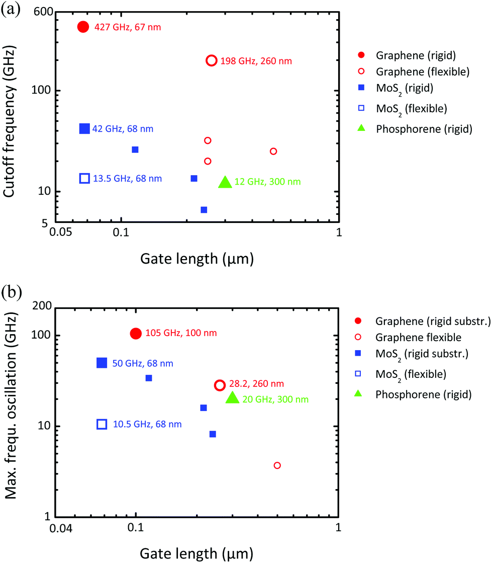 | ||
| Fig. 13 RF performance of 2D MOSFETs on flexible and rigid substrates. (a) Cutoff frequency fTvs. gate length. (b) Maximum frequency of oscillation fmaxvs. gate length. The respective record fT and fmax data are shown by large symbols. The numbers next to the record data points are the frequency (fT or fmax) and the gate length of the transistor. Data taken from ref. 179, 182, 187, 201, 205 and 206 for MOSFETs with graphene, from ref. 163 and 207 with MoS2, and from ref. 208 with phosphorene channels. | ||
To make the picture of flexible RF transistors complete, one should also consider the research on realizing ultrathin Si and InAs membranes and transferring them to flexible substrates. Based on this approach, 1.5 μm gate flexible Si MOSFETs showing an fT of 5.1 GHz and an fmax of 15.1 GHz203 and 75 nm gate flexible InAs-channel MOSFETs with fT = 105 GHz and fmax = 22.9 GHz204 have been reported. It should be noted that the bendability of the 2D materials is larger than that of the ultrathin Si and InAs membranes.12
Thus, the 2D materials are very promising for flexible electronics. Graphene is particularly interesting for flexible RF electronics while phosphorene and the TMDs are useful for both flexible digital and RF applications due to their semiconducting nature.
In 2015, the first silicene MOSFET was demonstrated.70 This back-gate device shows an on–off ratio of around 10 only due to the gapless silicene channel.
5.2 X-ane FETs
The current–voltage characteristics of graphane n- and p-channel MOSFETs have been simulated and, assuming ballistic carrier transport, on–off ratios of 105–106 have been obtained for a gate voltage swing of 0.8 V.210 Due to the fact that in graphane (in contrast to other bulk and 2D semiconductors) the electron effective mass is heavier than the hole effective mass, a higher on-current has been predicted for the p-channel MOSFET. Recently the first experimental graphane-like MOSFET has been reported.211 For this back-gate transistor with a hydrogenated graphene channel having a hydrogen coverage of 25% (compared to 100% for true graphane) and a gap of 4 eV, an on–off ratio of 3 × 10⁶ has been measured for a gate voltage swing of more than 40 V.5.3 TMD FETs
The first true 2D TMD transistor has been a 500 nm top-gate MOSFET with an exfoliated single-layer MoS2 channel reported in 2011.6 Due to the ≈2 eV bandgap of 2D MoS2, this device showed good switch-off and an on–off ratio of 108 for a gate voltage swing of 4 V. Subsequently other groups followed and fabricated MOSFETs with single- and multi-layer MoS2 channels. In most cases exfoliated MoS2 has been used, e.g.6,163,207 although also CVD-grown MoS2 has been reported.212 In addition to single transistors, recently simple circuits with MoS2 MOSFETs have been realized.212,213Since MoS2 is bendable,214 it is attractive for flexible electronics. Indeed, MoS2 MOSFETs on flexible substrates have been demonstrated.207,215 Due to their relatively low channel mobility, MoS2 MOSFETs show worse fT performance compared to graphene MOSFETs, see Fig. 13(a). They have, however, the big advantage of a semiconducting channel with a sufficiently wide gap leading to excellent switch-off as well as good drain current saturation and thus reasonable power gain and fmax. The current record RF performance for MoS2 MOSFETs is defined by a 68 nm gate transistor on a rigid SiO2/Si substrate showing an fT of 42 GHz and an fmax of 50 GHz and its counterpart on a flexible substrate with fT = 13.5 GHz and fmax = 10.5 GHz.207 Thus, MoS2 MOSFETs are very promising for flexible digital and RF applications.
While experimental work on TMD transistors has so far focused on MoS2 MOSFETs, recently the first single- and/or multi-layer WSe2,216 WS2,217 MoSe2,218 and MoTe2219 MOSFETs have been demonstrated.
On the theoretical side, a lot of work has been done too, particularly to investigate the advantages and drawbacks of TMD MOSFETs for future logic transistor generations and to compare their performance with that of Si MOSFETs. In ref. 220 and 221 it has been shown that in the ballistic limit TMD MOSFETs show slightly higher on-currents for a given off-current, i.e., better on–off ratios, than Si MOSFETs. It has also been shown that among the TMD MOSFETs those with tungsten-based channels show the highest on-currents due to the lower carrier effective mass compared to the Mo-based TMDs.220,222
As we have seen in Fig. 2, logic MOSFETs with gate lengths around 5 nm will be needed in 2028. This target was the motivation for numerous theoretical studies on the behavior of 5 nm gate MOSFETs.18,19,223 It has been shown that in such short channels direct source–drain tunneling becomes a serious issue, and that particularly high-mobility (and thus low-effective-mass) channels will suffer from unacceptably large tunneling currents. This suggests that channel materials with heavier carrier effective mass such as the TMDs would be a viable option. While the tunneling currents in 5 nm TMD channels have been analyzed by simulations,224 a study comparing the tunneling tendency of 5 nm Si and III–V channels with that of TMD channels is still missing. In the following we provide such a comparison for n-channel MOSFETs employing a simple first-order approximation.
In ref. 19 the source–drain tunneling current in III–V, Ge, and Si NW (nanowire) MOSFETs has been investigated. First, the band structure of the NWs has been calculated, and the bandgap and the carrier effective masses have been extracted (note that the band structure of small diameter NWs is different from that of the corresponding bulk material). These data and a simplified rectangular potential profile in the MOSFET channel have then been used to calculate the source–drain tunneling current in 5 nm NW n-channel MOSFETs. In the present study, we take both the electron effective masses for NWs with 6 nm diameter and the potential profile from ref. 19 and calculate the transmission coefficient TT through the barrier according to ref. 225
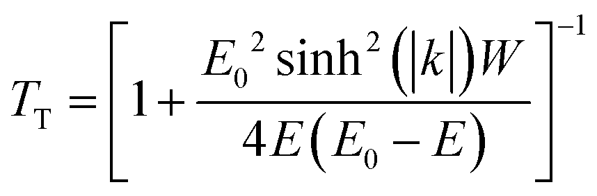 | (14) |
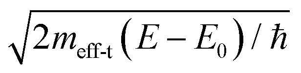 , where meff-t is the electron tunneling effective mass and ħ is the reduced Planck constant. The tunneling current IT is proportional to the transmission coefficient and can be estimated using
| IT ≈ cMTT | (15) |
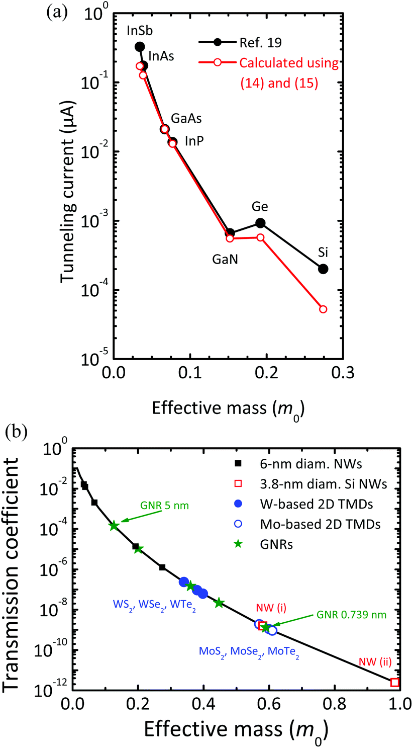 | ||
| Fig. 14 Tunneling behavior of 5 nm wide source–drain barriers. (a) Tunneling currents of 5 nm n-channel NW MOSFETs vs. electron tunneling effective mass of the barrier material from ref. 19 (blue curve) and calculated using eqn (14) and (15) with c = 10.4 μA. (b) Transmission coefficient through a 5 nm wide barrier vs. the electron effective mass of the barrier. Symbols indicate the calculated coefficients for 6 nm diameter NWs (black squares, from left to right InSb, InAs, GaAs, Ge, Si), 3.8 nm diameter strained Si NWs (red circles), W-based TMDs (blue circles, from left to right WS2, WSe2, WTe2), Mo-based TMDs (green circles, from left to right MoS2, MoSe2, MoTe2), and GNRs (olive stars, width from left to right 5, 3, 1.48, 1.11, and 0.74 nm). | ||
Fig. 14(b) shows the transmission coefficient through a 5 nm wide barrier as a function of the carrier effective mass of the channel material. The transmission coefficients have been calculated using eqn (14) and assuming the potential profile from ref. 19. Indicated by symbols are the transmission coefficients for selected 2D materials, 6 nm diameter Si, Ge, and III–V NWs using the effective masses from ref. 19, and different GNRs. As can be seen, the TMDs and the narrowest GNRs clearly outperform the III–V NWs in terms of tunneling. It should be noted that in narrow Si NWs the carrier effective mass can be tuned over a wide range by properly choosing the wire direction and strain.223 Therefore, in Fig. 14(b) the transmission coefficients for two compressively strained Si NWs with 3.8 nm diameter are included. NW (i) is <110> oriented and experiences −3 GPa strain leading to an electron effective mass of 0.581 × m0 and NW (ii) is <100> oriented, strained by −2 GPa, and shows an electron effective mass of 0.948 × m0.223 As can be seen, both NWs perform highly competitively in terms of tunneling. Thus, apart from TMDs and narrow GNRs, Si NWs are a possible option for the channels of beyond-roadmap MOSFETs. This leads us to the conclusion that Si remains a strong contender even at the end of and beyond the ITRS horizon.
Based on the results of our previous study, Fig. 15 shows a possible scenario for the choice of MOSFET channel materials. As discussed above and shown in Fig. 14(b), particularly the Mo-based TMDs, well-designed strained Si NWs, and narrow GNRs may become attractive beyond the horizon of the 2013 ITRS edition due to their reasonably heavy carrier effective mass.
 | ||
| Fig. 15 Possible scenario for the selection of the channel materials for logic MOSFETs. sSi means strained Si, μ is the carrier mobility, meff is the carrier effective mass, and 2Ds means semiconducting 2D materials. | ||
5.4 All-2D transistors
Recently transistors with multiple 2D materials in different device parts have been demonstrated.164,226–228 The general idea of all-2D MOSFETs is to use a suitable 2D material, e.g., MoS2 or WS2, for the channel, boron nitride as a gate dielectric, and gapless graphene for the contacts.6. Outlook
Research on 2D materials for electronic applications is a new field as can be seen from the fact that the first graphene, MoS2, and phosphorene MOSFETs have been reported in 2007, 2011, and 2014, respectively. Given this short history, the achievements made so far are remarkable and further progress is expected. On the other hand, it is extremely difficult to assess the real potential of the 2D materials in electronics. Table 11 lists, based on our current state of knowledge and provided that high-quality 2D layers can be realized in an industrial environment, our expectations on future applications of several 2D materials for MOSFET channels.| Material class | Material | Main pros | Main cons | Potential for | Not suited for |
|---|---|---|---|---|---|
| a The high mobility of germanene is yet to be confirmed. hp: high performance; mp: medium performance; flex: flexible. A question mark indicates that the advantages, drawbacks, and potential applications are not clear yet. | |||||
| X-enes | LA graphene | High μ | Zero gap | flex. mp RF | Logic, hp RF |
| GNRs | ? | Low μ | Logic at L < 5 nm | hp RF | |
| BLG | ? | Low μ, narrow gap | ? | Logic | |
| Silicene | ? | Zero gap | ? | Logic, hp RF | |
| Germanene | ? | Zero gap | ? | Logic, hp RF | |
| Phosphorene | Reasonable μ | ? | flex. mP RF & logic | Logic at L < 5 nm | |
| hp logic L > 5 nm | |||||
| X-anes | Germanane | High μa | ? | hp RF | Logic at L < 5nm |
| TMDs | Mo-based | Reasonable EG | Moderate μ | flex. mp RF & logic | hp RF |
| hp logic L ≤ 5nm | |||||
| W-based | Reasonable EG | Moderate μ | flex. Mp RF & logic | hp RF | |
Due to their zero gap, the gapless X-enes are not suitable for logic and high-performance RF FETs. The bendability and high mobility make graphene, however, a candidate for flexible medium-performance RF FETs. The semiconducting 2D materials with the exception of germanane suffer from low mobilities and therefore show only a little promise for high-performance logic (as long as source–drain tunneling is not an issue) and RF transistors, while they may find applications in flexible medium-performance logic and RF circuits. Due to their thinness (resulting in short scale lengths) and relatively heavy carrier effective mass (leading to suppressed source–drain tunneling) they may become an option for sub-5 nm logic FETs. It should be recognized, however, that multiple-gate Si NW transistors will be strong competitors in this field. In case germanane actually shows such a high mobility as predicted in ref. 53, it could become a very interesting material for high-performance logic and RF FETs.
We note that the fascinating variety of 2D materials is both a blessing and a curse – a blessing for researchers for whom the 2D materials are a new and wide field for exciting science, and a curse since the available funding for research spreads across many materials. Thus, sooner or later funding and research activities need to be focused on a limited number of promising 2D materials.
In conclusion we believe that research on 2D materials is just at the beginning and will stay a very exciting field. We are convinced that eventually certain 2D materials will find their applications in electronics, particularly since they can be used not only in transistors but also for other purposes, such as transparent electrodes, sensors, touch screen displays, etc., which are possibly closer to industrial fabrication than 2D transistors.
Acknowledgements
This work was supported by the Excellence Research and the Intra-Faculty Research Grants of Technische Universität Ilmenau, Germany, and by DFG under contract numbers SCHW 729/16-1 and PE 624/11-1. The authors would like to thank A. Alsioufy and M. Lootze for processing MoS2 and WS2 devices as well as F. Bechstedt, T. Heine and A. MacDonald for fruitful discussions and D. Akinwande for providing experimental results prior to its publication.References
- K. S. Novoselov, A. K. Geim, S. V. Morozov, D. Jiang, Y. Zhang, S. V. Dubonos, I. V. Grigorieva and A. A. Firsov, Science, 2004, 306, 666–669 CrossRef CAS PubMed.
- C. Berger, Z. Song, T. Li, X. Li, A. Y. Ogbazghi, R. Feng, Z. Dai, A. N. Marchenkov, E. H. Conrad, P. N. First and W. A. de Heer, J. Phys. Chem. B, 2004, 108, 19912–19916 CrossRef CAS.
- F. Schwierz, Proc. IEEE, 2013, 101, 1567–1584 CrossRef CAS.
- K. Bourzac, Nature, 2012, 483, S34–S36 CrossRef PubMed.
- M. Segal, Nature, 2012, 483, S43–S44 CrossRef CAS PubMed.
- B. Radisavljevic, A. Radenovic, J. Brivio, V. Giacometti and A. Kis, Nat. Nanotechnol., 2011, 6, 147–150 CrossRef CAS PubMed.
- The International Technology Roadmap for Semiconductors, http://www.itrs.net.
- S. Z. Butler, S. M. Hollen, L. Cao, Y. Cui, J. A. Gupta, H. R. Gutierrez, T. F. Heinz, S. S. Hong, J. Huang, A. F. Ischmach, E. Johnston-Halperin, M. Kuno, V. V. Plashnitsa, R. D. Robinson, R. S. Ruoff, S. Salahuddin, J. Shan, L. Shi, M. G. Spencer, M. Terrones, W. Windl and J. E. Goldberger, ACS Nano, 2013, 7, 2898–2926 CrossRef CAS PubMed.
- M. C. Lemme, L.-J. Li, T. Palacios and F. Schwierz, MRS Bull., 2014, 39, 711–718 CrossRef CAS.
- Q. H. Wang, K. Kalantar-Zadeh, A. Kis, J. N. Coleman and M. S. Strano, Nat. Nanotechnol., 2012, 7, 699–712 CrossRef CAS PubMed.
- G. Fiori, F. Bonaccorso, G. Iannaccone, T. Palacios, D. Neumaier, A. Seabaugh, S. K. Banerjee and L. Colombo, Nat. Nanotechnol., 2014, 9, 768–779 CrossRef CAS PubMed.
- D. Akinwande, N. Petrone and J. Hone, Nat. Commun., 2014, 5, 5678 CrossRef CAS PubMed.
- http://www.enterprisetech.com/2014/08/13/oracle-cranks-cores-32-sparc-m7-chip/ .
- G. E. Moore, Dig. ISSCC, 2003, 20–23 Search PubMed.
- J. A. del Alamo, Nature, 2011, 479, 317–323 CrossRef CAS PubMed.
- S. E. Thompson, G. Sun, Y. S. Choi and T. Nishida, IEEE Trans. Electron Devices, 2006, 53, 1010–1020 CrossRef CAS.
- H. Shang, M. M. Frank, E. P. Gusev, J. O. Chu, S. W. Bedell, K. W. Guarini and M. Ieong, IBM J. Res. Dev., 2006, 50, 377–386 CrossRef CAS.
- M. Luisier, M. Lundstrom, D. A. Antoniadis and J. Bokor, Tech. Dig. IEDM, 2011, 251–254 CAS.
- S. S. Sylvia, H.-Y. Park, M. A. Khayer, K. Alam, G. Klimeck and R. K. Lake, IEEE Trans. Electron Devices, 2012, 59, 2064–2069 CrossRef CAS.
- W. Baechtold, K. Daetwyler, T. Forster, T. O. Mohr, W. Walter and P. Wolf, Electron. Lett., 1973, 9, 232–234 CrossRef CAS.
- C. Huang, A. Herbig and R. Anderson, Dig. MTT-S, 1981, 25–27 Search PubMed.
- L. F. Lester, P. M. Smith, P. Ho, P. C. Chao, R. C. Tiberio, K. H. G. Du and E. D. Wolf, Tech. Dig. IEDM, 1988, 172–175 Search PubMed.
- L. D. Nguyen, D. C. Radulescu, P. J. Tasker, W. J. Schaff and L. F. Eastman, IEEE Electron Device Lett., 1988, 9, 374–376 CrossRef.
- L. D. Nguyen, P. J. Tasker, D. C. Radulescu and L. F. Eastman, IEEE Trans. Electron Devices, 1989, 36, 2243–2248 CrossRef.
- P. C. Chao, A. J. Tessmer, K.-H. G. Duh, P. Ho, M.-Y. Kao, P. M. Smith, J. M. Ballingall, S.-M. J. Liu and A. A. Jabra, IEEE Electron Device Lett., 1990, 11, 59–62 CrossRef CAS.
- P. Ho, M. Y. Kao, P. C. Chao, K. H. G. Duh, J. M. Ballingall, S. T. Allen, A. J. Tessmer and P. M. Smith, Electron. Lett., 1991, 27, 352–327 CrossRef.
- L. D. Nguyen, A. S. Brown, M. A. Thompson and L. M. Jelloian, IEEE Trans. Electron Devices, 1992, 39, 2007–2014 CrossRef CAS.
- P. C. Smith, S.-M. J. Liu, M.-Y. Kao, P. Ho, S. C. Wang, K. H. G. Duh, S. T. Fu and P. C. Chao, IEEE Microwave Guided Wave Lett., 1995, 5, 230–232 CrossRef.
- T. Suemitsu, T. Ishii, H. Yokoyama, Y. Umeda, T. Enoki, Y. Ishii and T. Tamamura, Tech. Dig. IEDM, 1998, 223–226 CAS.
- A. Endoh, Y. Yamashita, M. Higashiwaki, K. Hikosaka, T. Mimura, S. Hiyamizu and T. Matsui, Proc. IPRM, 2000, 87–90 CAS.
- Y. Yamashita, A. Endoh, K. Shinohara, T. Matsui, S. Hiyamizu and T. Mimura, IEEE Electron Device Lett., 2002, 23, 573–575 CrossRef CAS.
- R. Lai, X. B. Mei, W. R. Deal, W. Yoshida, Y. M. Kim, P. H. Liu, J. Lee, J. Uyeda, V. Radisic, M. Lange, T. Gaier, L. Samoska and A. Fung, Tech. Dig. IEDM, 2007, 609–611 CAS.
- S.-J. Yeon, M. Park, J. Choi and K. Seo, Tech. Dig. IEDM, 2007, 613–616 CAS.
- D.-H. Kim and J. A. del Alamo, IEEE Electron Device Lett., 2008, 23, 830–833 CrossRef.
- R. Lai, W. R. Deal, X. B. Mei, W. Yoshida, J. Lee, D. Dang, J. Wang, Y. M. Kim, P. H. Liu, V. Radisic, M. Lange, T. Gaier, L. Samoska and A. Fung, Proc. IPRM, 2008, 1–3 CAS.
- W. Deal, X. B. Mei, K. M. K. H. Leong, V. Radisic, S. Sakozy and R. Lai, IEEE Trans. THz Sci. Technol., 2011, 1, 25–32 CrossRef CAS.
- D.-H. Kim, B. Brar and J. A. del Alamo, Tech. Dig. IEDM, 2011, 319–322 CAS.
- M. Schlechtweg, A. Tessmann, I. Kallfass, A. Leuther, V. Hurm, H. Massler, M. Riessle, R. Lösch and O. Ambacher, Proc. NEWCAS, 2011, 269–272 Search PubMed.
- A. Leuther, A. Tessmann, M. Dammann, H. Massler, M. Schlechtweg and O. Ambacher, Proc. IPRM, 2013, 1–2 Search PubMed.
- D. L. Woolard, E. R. Brown, M. Pepper and M. Kemp, Proc. IEEE, 2005, 93, 1722–1743 CrossRef CAS.
- M. Tonouchi, Nat. Photonics, 2007, 1, 97–105 CrossRef CAS.
- J.-P. Colinge, C.-W. Lee, A. Afzalian, N. D. Akhavan, R. Yan, I. Ferain, P. Razavi, B. O'Neill, A. Blake, M. White, A.-M. Kelleher, B. McCarthy and R. Murphy, Nat. Nanotechnol., 2010, 5, 225–229 CrossRef CAS PubMed.
- F. Schwierz, H. Wong and J. J. Liou, Nanometer CMOS, Pan Stanford Publishing, Singapore, 2010 Search PubMed.
- F. Schwierz and J. J. Liou, Modern Microwave Transistors, J. Wiley & Sons, Hoboken, 2003 Search PubMed.
- P. Miro, M. Audiffred and T. Heine, Chem. Soc. Rev., 2014, 43, 6537–6554 RSC.
- P. Vogt, P. De Padova, C. Quaresima, J. Avila, E. Frantzeskakis, M. C. Asensio, A. Resta, B. Ealet and G. Le Lay, Phys. Rev. Lett., 2012, 108, 155501 CrossRef PubMed.
- M. E. Davila, L. Xian, S. Cahangirov, A. Rubio and G. Le Lay, New J. Phys., 2014, 16, 095002 CrossRef.
- L. Li, Y. Yu, G. J. Ye, Q. Ge, X. Ou, H. Wu, D. Feng, X. H. Chen and Y. Zhang, Nat. Nanotechnol., 2014, 9, 372–377 CrossRef CAS PubMed.
- B. van den Broek, M. Houssa, E. Scarlise, G. Pourtois, V. V. Afanas'ev and A. Stesmans, 2D Mater., 2014, 1, 021004 CrossRef.
- http://apps.webofknowledge.com/ .
- J. O. Sofo, A. S. Chaudhari and G. D. Barber, Phys. Rev. B: Condens. Matter, 2007, 75, 153401 CrossRef.
- D. C. Elias, R. R. Nair, T. M. G. Mohiuddin, S. V. Morozov, P. Blake, M. P. Halsall, A. C. Ferrari, D. W. Boukhvalov, M. I. Katsnelson, A. K. Geim and K. S. Novoselov, Science, 2010, 323, 610–613 CrossRef PubMed.
- E. Bianco, S. Butler, S. Jiang, O. D. Restrepo, W. Windl and J. E. Goldberger, ACS Nano, 2013, 7, 4414–4421 CrossRef CAS PubMed.
- R. R. Nair, W. C. Ren, R. Jalil, I. Riaz, V. G. Kravets, L. Britnell, P. Blake, F. Schedin, A. S. Mayorov, S. J. Yuan, M. I. Katsnelson, H. M. Cheng, W. Strupinski, L. G. Bulusheva, A. V. Okotrub, I. V. Grigorieva, A. N. Grigorenko, K. S. Novoslov and A. K. Geim, Small, 2010, 6, 2877–2884 CrossRef CAS PubMed.
- J. T. Robinson, J. S. Burgess, C. E. Junkermeier, S. C. Badescu, T. L. Reinecke, F. K. Perkins, M. K. Zalalutdniov, J. W. Baldwin, J. C. Culbertson, P. E. Sheehan and E. S. Snow, Nano Lett., 2010, 10, 3001–3005 CrossRef CAS PubMed.
- A. Kuc, in Chemical Modelling: 11, ed. M. Springborg and J.-O. Joswig, 2015, pp. 1–29 Search PubMed.
- A. P. Nayak, T. Pandey, D. Voiry, J. Liu, S. T. Moran, A. Sharma, C. Tan, C.-H. Chen, L.-J. Li, M. Chhowalla, J.-F. Lin, A. K. Singh and D. Akinwande, Nano Lett., 2015, 15, 346–353 CrossRef CAS PubMed.
- G. Eda, T. Fujita, H. Yamaguchi, D. Voiry, M. Chen and M. Chhowalla, ACS Nano, 2012, 6, 7311–7317 CrossRef CAS PubMed.
- M. Naguib, O. Mashtalir, J. Carle, V. Presser, J. Lu, L. Hultman, Y. Gogotsi and M. W. Barsoum, ACS Nano, 2012, 6, 1322–1331 CrossRef CAS PubMed.
- M. Naguib, M. Kurtogly, V. Presser, J. Lu, J. Niu, M. Heon, L. Hultman, Y. Gogotsi and M. W. Barsoum, Adv. Mater., 2011, 23, 4248–4253 CrossRef CAS PubMed.
- M. Naguib, J. Come, B. Dyatkin, V. Presser, P.-L. Taberna, P. Simon, M. W. Barsoum and Y. Gogotsi, Electrochem. Commun., 2012, 16, 61–64 CrossRef CAS.
- M. Khazaei, M. Arai, T. Sasaki, C.-Y. Chung, N. S. Venkataramanan, M. Estili, Y. Sakka and Y. Kawazoe, Adv. Funct. Mater., 2013, 23, 2185–2192 CrossRef CAS.
- H. Sahin, C. Cahangirov, M. Topsakal, E. Bekaroglu, E. Akturk, R. T. Senger and S. Ciraci, Phys. Rev. B: Condens. Matter, 2009, 80, 155453 CrossRef.
- H. L. Zhuang, A. K. Singh and R. Hennig, Phys. Rev. B: Condens. Matter, 2013, 87, 165415 CrossRef.
- V. Nicolosi, M. Chhowalla, M. G. Kanatzidis, M. S. Strano and J. N. Coleman, Science, 2013, 340, 1420 CrossRef CAS.
- Y.-M. Lin, C. Dimitrakopoulos, K. A. Jenkins, D. B. Farmer, H.-Y. Chiu, A. Grill and P. Avouris, Science, 2010, 327, 662 CrossRef CAS PubMed.
- L. Colombo, R. M. Wallace and R. S. Ruoff, Proc. IEEE, 2013, 101, 1536–1556 CrossRef CAS.
- Y.-H. Lee, L. Yu, H. Wang, W. Fang, X. Ling, Y. Shi, C.-T. Lin, J.-K. Huang, M.-T. Chang, C.-S. Chang, M. Dresselhaus, T. Palacios, L.-J. Li and J. Kong, Nano Lett., 2013, 13, 1852–1857 CAS.
- H. Zhou, C. Wang, J. C. Shaw, R. Cheng, Y. Chen, X. Huang, Y. Liu, N. O. Weiss, Z. Lin, Y. Huang and X. Duan, Nano Lett., 2015, 15, 709–713 CrossRef CAS PubMed.
- L. Tao, E. Cinquanta, D. Chiappe, C. Granzianetti, M. Fanciulli, M. Dubey, A. Molle and D. Akinwande, Nat. Nanotechnol., 2015, 10, 227–231 CrossRef CAS PubMed.
- J. C. Bean, in High-Speed Semiconductor Devices, ed. S. M. Sze, J. Wiley, 1990 Search PubMed.
- K. Kim, J.-Y. Choi, S.-H. Cho and H.-J. Chung, Nature, 2011, 479, 338–344 CrossRef CAS PubMed.
- F. Schwierz, Nat. Nanotechnol., 2010, 5, 487–496 CrossRef CAS PubMed.
- D. Reddy, L. F. Register, G. D. Carpenter and S. K. Banerjee, J. Phys. D: Appl. Phys., 2011, 44, 313001 CrossRef.
- D.-H. Kim, B. Brar and J. A. del Alamo, Tech. Dig. IEDM, 2011, 319–322 CAS.
- A. Leuther, A. Tessmann, M. Dammann, H. Massler, M. Schlechtweg and O. Ambacher, Proc. IPRM, 2013, 1–2 Search PubMed.
- T. Ashley, L. Buckle, M. T. Emeny, M. Fearn, D. G. Hayes, K. P. Hilton, R. Jefferies, T. Martin, T. J. Phillips, J. Powell, A. W.-H. Tang, D. Wallis and P. J. Wilding, Proc. CSIC, 2006, 121–124 CAS.
- T. Ashley, M. T. Emeny, D. G. Hayes, K. P. Hilton, R. Jefferies, J. O. Maclean, S. J. Smith, A. W.-H. Tang, D. Wallis and P. J. Webber, Tech. Dig. IEDM, 2009, 849–852 Search PubMed.
- E. Pop, V. Varshney and A. K. Roy, MRS Bull., 2012, 37, 1273–1281 CrossRef CAS.
- R.-H. Yan, A. Ourmazd and K. F. Lee, IEEE Trans. Electron Devices, 1992, 39, 1704–1710 CrossRef CAS.
- Q. Zhang, Y. Lu, H. G. Xing, S. J. Koester and S. O. Koswatta, IEEE Electron Device Lett., 2010, 31, 531–533 CrossRef CAS.
- Q. Zhang, Y. Lu, G. H. Xing, C. A. Richter, S. J. Koester and S. O. Koswatta, Proc. DRC, 2010, 75–76 Search PubMed.
- M. V. Fischetti, T. P. O'Regan, S. Narayanan, C. Sachs, S. Jin, J. Kim and Y. Zhang, IEEE Trans. Electron Devices, 2007, 54, 2116–2136 CrossRef CAS.
- S. Kümmel and L. Kronik, Rev. Mod. Phys., 2008, 80, 3–60 CrossRef.
- J. C. Garcia, D. B. De Lima, L. V. C. Assali and J. F. Justo, J. Phys. Chem. C, 2011, 115, 13242–13246 CAS.
- M. Houssa, E. Scalise, K. Sankaran, G. Pourtois, V. V. Afanas'ev and A. Stesmans, Appl. Phys. Lett., 2011, 98, 223107 CrossRef.
- L. Yang, C.-H. Park, Y.-W. Son, M. L. Cohen and S. G. Louie, Phys. Rev. Lett., 2007, 99, 186801 CrossRef PubMed.
- D. Gunlycke and C. T. White, Phys. Rev. B: Condens. Matter, 2008, 77, 115116 CrossRef.
- P. Ruffieux, J. Cai, N. Plumb, L. Patthey, D. Prezzi, A. Ferretti, E. Molinari, X. Feng, K. Müllen, C. A. Pignedoli and R. Fasel, ACS Nano, 2012, 6, 6930–6935 CrossRef CAS PubMed.
- S. Linden, D. Zhong, A. Timmer, N. Aghdassi, J. H. Franke, H. Zhang, X. Feng, K. Müllen, H. Fuchs, L. Chi and H. Zacharias, Phys. Rev. Lett., 2012, 108, 216801 CrossRef CAS PubMed.
- X. Li, X. Wang, L. Zhang, S. Lee and H. Dai, Science, 2008, 319, 1229–1232 CrossRef CAS PubMed.
- J. Cai, P. Ruffieux, R. Jaafar, M. Bieri, T. Braun, S. Blankenburg, M. Muoth, A. P. Seitsonen, M. Saleh, X. Feng, K. Müllen and R. Fasel, Nature, 2010, 466, 470–473 CrossRef CAS PubMed.
- M. Y. Han, B. Özyilmaz, Y. Zhang and P. Kim, Phys. Rev. Lett., 2007, 98, 206805 CrossRef PubMed.
- L. Tapaszto, G. Dobrik, P. Lambin and L. P. Biro, Nat. Nanotechnol., 2008, 3, 397–401 CrossRef CAS PubMed.
- Y.-C. Chen, D. G. de Oteyza, Z. Pedramrazi, C. Chen, F. R. Fischer and M. F. Crommie, ACS Nano, 2013, 7, 6123–6128 CrossRef CAS PubMed.
- E. V. Castro, K. S. Novoselov, S. V. Morozov, N. M. R. Peres, J. M. B. Lopes dos Santos, J. Nilsson, F. Guinea, A. K. Geim and A. H. Castro Netro, Phys. Rev. Lett., 2007, 99, 216802 CrossRef PubMed.
- G. Iannaccone, G. Fiori, M. Macucci, P. Michetti, M. Cheli, A. Betti and P. Marconcini, Tech. Dig. IEDM, 2009, 245–248 Search PubMed.
- S. Cahangirov, M. Topsakal and S. Ciraci, Phys. Rev. B: Condens. Matter, 2010, 81, 195120 CrossRef.
- Z. Ni, Q. Liu, K. Tang, J. Zheng, J. Zhou, R. Qin, Z. Gao, D. Yu and J. Lu, Nano Lett., 2012, 12, 113–118 CrossRef CAS PubMed.
- H. Liu, A. T. Neal, Z. Zhu, Z. Luo, X. Xu, D. Tomanek and P. D. Ye, ACS Nano, 2014, 8, 4033–4041 CrossRef CAS PubMed.
- Y. Xie and P. R. C. Kent, Phys. Rev. B: Condens. Matter, 2013, 87, 235441 CrossRef.
- I. Meric, C. R. Dean, N. Petrone, L. Wang, J. Hone, P. Kim and K. L. Shepard, Proc. IEEE, 2013, 101, 1609–1619 CrossRef CAS.
- W. Gannett, W. Regan, K. Watanabe, T. Taniguchi, M. F. Crommie and A. Zettl, Appl. Phys. Lett., 2011, 98, 242105 CrossRef.
- X. Li, J. T. Mullen, Z. Jinn, K. M. Borysenko, M. B. Nardelli and K. W. Kim, Phys. Rev. B: Condens. Matter, 2013, 87, 115418 CrossRef.
- Z.-G. Shao, X.-S. Ye, L. Yang and C.-L. Wang, J. Appl. Phys., 2013, 114, 093712 CrossRef.
- O. D. Restrepo, K. E. Krymowski, J. Goldberger and W. Windl, New J. Phys., 2014, 16, 105009 CrossRef.
- K. Kaasbjerg, K. S. Thygesen and K. W. Jacobsen, Phys. Rev. B: Condens. Matter, 2012, 85, 115317 CrossRef.
- L. Zeng, Z. Xie, S. Chen, G. Du, J. Kang and X. Liu, Appl. Phys. Lett., 2013, 103, 113505 CrossRef.
- W. Bao, X. Cai, D. Kim, K. Sridhara and M. S. Fuhrer, Appl. Phys. Lett., 2013, 102, 042104 CrossRef.
- S. Das, H.-Y. Chen, A. V. Penumatcha and J. Appenzeller, Nano Lett., 2013, 13, 100–105 CrossRef CAS PubMed.
- J. Lee, H.-Y. Chang, T.-J. Ha, H. Li, R. S. Ruoff, A. Dodabalapu and D. Akinwande, Tech. Dig. IEDM, 2013, 491–494 Search PubMed.
- W. Liu, J. Kang, W. Cao, D. Sarkar, Y. Khatami, D. Jena and K. Banerjee, Tech. Dig. IEDM, 2013, 499–502 CAS.
- S. Larentis, B. Fallahazad and E. Tutuc, Appl. Phys. Lett., 2012, 101, 223104 CrossRef.
- W. Liu, J. Kang, D. Sarkar, Y. Khatami, D. Jena and K. Banerjee, Nano Lett., 2013, 13, 1983–1990 CrossRef CAS PubMed.
- Y. Wang, B.-C. Huang, M. Zhang, C. Miao, Y.-H. Xie and J. C. S. Woo, Dig. VLSI Technol., 2011, 116–117 Search PubMed.
- J. Y. Tan, A. Avsar, J. Balakrishnan, G. K. W. Koon, T. Taychatanapat, E. C. T. O'Farrell, K. Watanabe, T. Taniguchi, G. Eda, A. H. Castro Neto and B. Özyilmaz, Appl. Phys. Lett., 2014, 104, 183504 CrossRef.
- X. Li, C. W. Magnuson, A. Venugopal, J. An, J. W. Suk, B. Han, M. Borysiak, W. Cai, A. Velamakanni, Y. Zhu, L. Fu, E. M. Vogel, E. Voelkl, L. Colombo and R. S. Ruoff, Nano Lett., 2010, 10, 4328–4334 CrossRef CAS PubMed.
- J. A. Robinson, M. Hollander, M. LaBella, K. A. Trumbull, R. Cavalero and D. W. Snyder, Nano Lett., 2011, 11, 3875–3880 CrossRef CAS PubMed.
- Z. Guo, R. Dong, P. S. Chakraborty, N. Lourenco, J. Palmer, Y. Hu, M. Ruan, J. Hankinson, J. Kunc, J. D. Cressler, C. Berger and W. A. de Heer, Nano Lett., 2013, 13, 942–947 CrossRef CAS PubMed.
- J.-H. Chen, C. Jang, S. Xiao, M. Ishigami and M. S. Fuhrer, Nat. Nanotechnol., 2008, 3, 206–209 CrossRef CAS PubMed.
- D. Lembke and A. Kis, ACS Nano, 2012, 6, 10070–10075 CrossRef CAS PubMed.
- M. S. Fuhrer and J. Hone, Nat. Nanotechnol., 2013, 8, 146–147 CrossRef CAS PubMed.
- B. Radislavjevic and A. Kis, Nat. Nanotechnol., 2013, 8, 147–148 CrossRef PubMed.
- S. Jo, N. Ubrig, H. Berger, A. B. Kuzmenko and A. Morpurgo, Nano Lett., 2014, 14, 2019–2025 CrossRef CAS PubMed.
- D. Ovchinnikov, A. Allain, Y.-S. Huang, D. Dumcenco and A. Kis, ACS Nano, 2014, 8, 8174–8181 CrossRef CAS PubMed.
- H. Fang, S. Chuang, T. C. Chang, K. Takei, T. Takahashi and A. Javey, Nano Lett., 2012, 12, 3788–3792 CrossRef CAS PubMed.
- A. Allain and A. Kis, ACS Nano, 2014, 8, 7180–7185 CrossRef CAS PubMed.
- L. Li, Y. Yu, G. J. Ye, Q. Ge, X. Ou, H. Wu, D. Feng, X. H. Chen and Y. Zhang, Nat. Nanotechnol., 2014, 9, 372–377 CrossRef CAS PubMed.
- V. E. Dorgan, M.-H. Bae and E. Pop, Appl. Phys. Lett., 2010, 97, 082112 CrossRef.
- M. Bresciani, A. Paussa, P. Palestri, D. Esseni and L. Selmi, Tech. Dig. IEDM, 2010, 724–727 CAS.
- X. Li, K. M. Borysenko, M. B. Nardelli and K. W. Kim, Phys. Rev. B: Condens. Matter, 2011, 84, 195453 CrossRef.
- A. Betti, G. Fiori and G. Iannaccone, Appl. Phys. Lett., 2011, 99, 242108 CrossRef.
- R. Granzner, V. M. Polyakov, C. Schippel and F. Schwierz, IEEE Trans. Electron Devices, 2014, 61, 3601–3607 CrossRef CAS.
- M. Schmidt, M. C. Lemme, H. D. B. Gottlob, F. Driussi, L. Selmi and H. Kurz, Solid-State Electron., 2009, 53, 1246–1251 CrossRef CAS.
- H. Raza and E. C. Kan, Phys. Rev. Lett., 2008, 77, 245434 Search PubMed.
- K.-T. Lam, Z. Dong and J. Guo, IEEE Electron Device Lett., 2014, 35, 963–965 CrossRef CAS.
- J. Qiao, X. Kong, Z.-X. Hu, F. Yang and W. Ji, Nat. Commun., 2014, 5, 4475 CAS.
- A. A. Balandin, S. Gosh, W. Bao, I. Calizo, D. Teweldebrhan, F. Miao and C. N. Lau, Nano Lett., 2008, 8, 902–907 CrossRef CAS PubMed.
- E. Pop, V. Varshney and A. K. Roy, MRS Bull., 2012, 37, 1273–1281 CrossRef CAS.
- C. Muratore, V. Varshney, J. J. Gengler, J. J. Hu, J. E. Bultman, T. M. Smith, P. J. Shamberger, B. Qiu, X. Ruan, A. K. Roy and A. A. Voevodin, Appl. Phys. Lett., 2013, 102, 081604 CrossRef.
- J. H. Seol, I. Jo, A. L. Moore, L. Lindsay, Z. H. Aitken, M. T. Pettes, X. Li, Z. Yao, R. Huang, D. Broido, N. Mingo, R. S. Ruoff and L. Shi, Science, 2010, 328, 213–216 CrossRef CAS PubMed.
- A. D. Liao, J. Z. Wu, X. Wang, K. Tahy, D. Jena, H. Dai and E. Pop, Phys. Rev. Lett., 2011, 106, 256801 CrossRef PubMed.
- R. Yan, J. R. Simpson, S. Bertolazzi, J. Brivio, M. Watson, X. Wu, A. Kis, T. Luo, A. R. H. Walker and H. G. Xing, ACS Nano, 2014, 8, 986–993 CrossRef CAS PubMed.
- X. Gu and R. Yang, Appl. Phys. Lett., 2014, 105, 131903 CrossRef.
- K. F. Mak, C. H. Lui and T. F. Heinz, Appl. Phys. Lett., 2010, 97, 221904 CrossRef.
- Z. Chen, W. Jang, W. Bao, C. N. Lau and C. Dames, Appl. Phys. Lett., 2009, 95, 161910 CrossRef.
- S. S. Mahajan, G. Subbarayan and B. G. Sammakia, IEEE Trans. Comp., Packag., Manuf. Technol., 2011, 1, 1132–1139 CrossRef CAS.
- J. Chen, G. Zhang and B. Li, J. Appl. Phys., 2012, 112, 064319 CrossRef.
- R. Mao, B. D. Kong, K. W. Kim, T. Jayasekera, A. Calzolari and M. B. Nardelli, Appl. Phys. Lett., 2012, 101, 113111 CrossRef.
- B. Deng, A. Chernatynskiy, M. Khafizov, D. H. Hurley and S. R. Phillpot, J. Appl. Phys., 2014, 115, 084910 CrossRef.
- D. H. Hurley, M. Khafizov and S. L. Shinde, J. Appl. Phys., 2011, 109, 083504 CrossRef.
- M.-H. Bae, S. Islam, V. E. Dorgan and E. Pop, ACS Nano, 2011, 5, 7936–7944 CrossRef CAS PubMed.
- Z.-Y. Ong, M. V. Fischetti, A. Y. Serov and E. Pop, Phys. Rev. B: Condens. Matter, 2013, 87, 195404 CrossRef.
- K. Nagashio, T. Nishimura, K. Kita and A. Toriumi, Tech. Dig. IEDM, 2009, 565–568 Search PubMed.
- W. S. Leong, H. Gong and J. T. L. Thong, ACS Nano, 2014, 8, 994–1001 CrossRef CAS PubMed.
- J. S. Moon, M. Antcliffe, H. C. Seo, D. Curtis, S. Lin, A. Schmitz, I. Milosavljevic, A. A. Kiselev, R. S. Ross, D. K. Gaskill, P. M. Campbell, R. C. Fitch, K.-M. Lee and P. Asbeck, Appl. Phys. Lett., 2012, 100, 203512 CrossRef.
- F. Xia, V. Perebeinos, Y.-M. Lin, Y. Wu and P. Avouris, Nat. Nanotechnol., 2011, 6, 179–184 CrossRef CAS PubMed.
- I. Meric, C. R. Dean, A. F. Young, N. Baklitskaya, N. J. Tremblay, C. Nuckolls, P. Kim and K. L. Sheppard, Nano Lett., 2011, 11, 1093–1097 CrossRef CAS PubMed.
- L. Yang, K. Majumdar, Y. Du, H. Liu, H. Wu, M. Hatzistergos, P. Y. Hung, R. Tieckelmann, W. Tsai, C. Hobbs and P. D. Ye, Dig. VLSI Technol., 2014, 1–2 Search PubMed.
- R. Kappera, D. Voiry, S. E. Yalcin, B. Branch, G. Gupta, A. D. Mohite and M. Chhowalla, Nat. Mater., 2014, 13, 1128–1134 CrossRef CAS PubMed.
- W. Liu, J. Kang, W. Cao, D. Sarkar, Y. Khatami, D. Jena and K. Banerjee, Tech. Dig. IEDM, 2013, 499–502 CAS.
- C. D. English, G. Shine, V. E. Dorgan, K. C. Saraswat and E. Pop, Proc. DRC, 2014, 193–194 Search PubMed.
- D. Krasnozhon, D. Lembke, C. Nyffeler, Y. Leblebici and A. Kis, Nano Lett., 2014, 14, 5905–5911 CrossRef CAS PubMed.
- S. Das, R. Gulotty, A. V. Sumant and A. Roelofs, Nano Lett., 2014, 14, 2861–2866 CrossRef CAS PubMed.
- H.-J. Chuang, X. Tan, N. J. Ghimire, M. M. Parera, B. Chamberlain, M. M.-C. Cheng, J. Yan, D. Mandrus, D. Tomanek and Z. Zhou, Nano Lett., 2014, 14, 3594–3601 CrossRef CAS PubMed.
- Y. Du, H. Liu, Y. Deng and P. D. Ye, ACS Nano, 2014, 10, 10035–10042 CrossRef PubMed.
- S. M. Koh, E. Y.-J. Kong, B. Liu, C.-M. Ng, G. S. Samudra and Y.-C. Yeo, IEEE Trans. Electron Devices, 2011, 58, 3852–3862 CrossRef CAS.
- A. R. Alt and C. R. Bolognesi, IEEE Trans. Electron Devices, 2013, 60, 787–792 CrossRef CAS.
- H. Li, Z. Feng, C. W. Tang and K. M. Lau, IEEE Electron Device Lett., 2011, 32, 1224–1226 CrossRef CAS.
- Y. Wu, D. B. Farmer, F. Xia and P. Avouris, Proc. IEEE, 2013, 101, 1620–1637 CrossRef CAS.
- A. Hsu, H. Wang, Y. C. Shin, B. Mailly, X. Zhang, L. Yu, Y. Shi, Y. H. Lee, M. Dubey, K. K. Kim, J. Kong and T. Palacios, Proc. IEEE, 2013, 101, 1638–1652 CrossRef CAS.
- X. Wang, Y. Ouyang, X. Li, H. Wang, J. Guo and H. Dai, Phys. Rev. Lett., 2008, 100, 206803 CrossRef PubMed.
- M.-W. Lin, C. Ling, Y. Zhang, H. J. Yoon, M. M.-C. Cheng, L. A. Agapito, N. Kioussis, N. Widjaja and Z. Zhou, Nanotechnology, 2011, 22, 265201 CrossRef PubMed.
- H. Yang, J. Heo, S. Park, H. J. Song, D. H. Seo, K.-E. Byun, P. Kim, I. Yoo, H.-J. Chung and K. Kim, Science, 2012, 336, 1140–1143 CrossRef CAS PubMed.
- L. Britnell, R. V. Gorbatchev, R. Jalil, B. D. Belle, F. Schedin, A. Mishchenko, T. Georgiou, M. I. Katsnelson, L. Eaves, S. V. Morozov, N. M. R. Peres, J. Leist, A. K. Geim, K. S. Novoselov and L. A. Ponomarenko, Science, 2012, 335, 947–950 CrossRef CAS PubMed.
- W. Mehr, J. Dabrowski, J. C. Scheytt, G. Lippert, Y.-H. Xie, M. C. Lemme, M. Ostling and G. Lupina, IEEE Electron Device Lett., 2012, 33, 691–693 CrossRef CAS.
- M. C. Lemme, T. J. Echtermeyer, M. Baus and H. Kurz, IEEE Electron Device Lett., 2007, 28, 282–284 CrossRef CAS.
- I. Meric, N. Baklitskaya, P. Kim and K. L. Shepard, Tech. Dig. IEDM, 2008, 1–4 Search PubMed.
- R. Cheng, J. Bai, L. Liao, H. Zhou, Y. Chen, L. Liu, Y.-C. Lin, S. Jiang, Y. Huang and X. Duan, Proc. Natl. Acad. Sci. U. S. A., 2012, 109, 11588–11592 CrossRef CAS PubMed.
- Y. Wu, K. A. Jenkins, A. Valdes-Garcia, D. B. Farmer, Y. Zhu, A. A. Bol, C. Dimitrakopoulos, W. Zhu, F. Xia, P. Avouris and Y.-M. Lin, Nano Lett., 2012, 12, 3062–3067 CrossRef CAS PubMed.
- L. Liao, Y.-C. Lin, M. Bao, R. Cheng, J. Bai, Y. Liu, Y. Qu, K. L. Wang, Y. Huang and X. Duan, High-speed graphene transistors with a self-aligned nanowire gate, Nature, 2010, 467, 305–308 CrossRef CAS PubMed.
- Z. H. Feng, C. Yu, J. Li, Q. B. Liu, Z. Z. He, X. B. Song, J. J. Wang and S. J. Cai, Carbon, 2014, 75, 249–254 CrossRef CAS.
- D.-H. Kim and J. A. del Alamo, 30-nm InAs PHEMTs with fT=644 GHz and fmax=681 GHz, IEEE Electron Device Lett., 2010, 31, 806–808 CrossRef CAS.
- S. Lee, B. Jagannathan, S. Narasimha, A. Chou, N. Zamdmer, J. Johnson, R. Williams, L. Wagner, J. Kim, J.-O. Plouchart, J. Pekarik, S. Springer and G. Freeman, Tech. Dig. IEDM, 2007, 255–258 CAS.
- I. Post, M. Akbar, G. Curello, S. Gannavaram, W. Hafez, U. Jalan, K. Komeyli, J. Lin, N. Lindert, J. Park, J. Rizk, G. Sacks, C. Tsai, D. Yeh, P. Bai and C.-H. Jan, Tech. Dig. IEDM, 2006, 1–3 Search PubMed.
- C.-H. Jan, P. Bai, S. Biwas, M. Buehler, Z.-P. Chen, G. Curello, S. Gannavaram, W. Hafez, J. He, J. Hicks, U. Jalan, N. Lazo, J. Lin, N. Lindert, C. Litteken, M. Jones, M. Kang, K. Komeyli, A. Mezhiba, S. Naskar, S. Olson, J. Park, R. Parker, L. Pei, I. Post, N. Pradhan, C. Prasad, M. Prince, J. Rizk, G. Sacks, H. Tashiro, D. Towner, C. Tsai, Y. Wang, L. Yang, J.-Y. Yeh, J. Yip and K. Misty, Tech. Dig. IEDM, 2008, 1–3 Search PubMed.
- N. Petrone, I. Meric, T. Chari, K. L. Shepard and J. Hone, J. Electron Device Soc., 2015, 3, 44–48 CrossRef.
- M. Tanzid, M. A. Anderson, J. Sun and J. Stake, Appl. Phys. Lett., 2014, 104, 013502 CrossRef.
- D. Mele, S. Fregonese, S. Lepilliet, E. Pichonat, G. Dambrine and H. Happy, IMS Dig., 2013, 1–4 Search PubMed.
- B. Hughes, IEEE Trans. Microwave Theory Tech., 1992, 40, 1821–1832 CrossRef.
- P. C. Chao, A. J. Tessmer, K.-H. G. Du, P. Ho, M.-Y. Kao, P. M. Smith, J. M. Ballingall, S.-M. J. Liu and A. A. Jabra, IEEE Electron Device Lett., 1990, 11, 59–62 CrossRef CAS.
- P. Ho, P. C. Chao, K. H. G. Duh, A. A. Jabra, J. M. Ballingall and P. M. Smith, Tech. Dig. IEDM, 1988, 184–186 Search PubMed.
- W. E. Hoke, P. J. Lemonias, J. J. Mosca, P. S. Lyman, A. Torabi, P. F. Marsh, R. A. McTaggart, S. M. Lardizabal and K. Hetzler, JVST B, 1999, 13, 1131–1135 Search PubMed.
- M. Schlechtweg, A. Tessmann, A. Leuther, H. Massler, S. Wagner, R. Aidam, J. Rosenzweig and O. Ambacher, Proc. COMCAS, 2013, 1–4 Search PubMed.
- J.-H. Lee, H.-S. Yoon, C.-S. Park and H.-M. Park, IEEE Electron Device Lett., 1995, 16, 271–273 CrossRef CAS.
- D. Geiger, M. Mittermeier, J. Dickmann, C. Geng, F. Scholz and E. Kohn, Electron. Lett., 1995, 31, 1295–1297 CrossRef CAS.
- L. F. Tiemeijer, H. M. J. Boots, R. J. Havens, A. J. Scholten, P. H. W. de Vreede, P. H. Woerlee, A. Heringa and D. B. M. Klaassen, Tech. Dig. IEDM, 2001, 223–226 Search PubMed.
- K. Kuhn, R. Basco, D. Becher, M. Hattendorf, P. Packan, I. Post, P. Vandervoorn and I. Young, Dig. VLSI Symp., 2004, 224–225 CAS.
- F. Schwierz, Graphene electronics, in Emerging nanoelectronic devices, ed. A. Chen, J. Hutchby, V. Zhirnov and G. Bourianoff, J. Wiley & Sons, 2015 Search PubMed.
- I. Imperiale, S. Bonsignore, A. Gnudi, E. Gnani, S. Reggiani and G. Baccarani, Tech. Dig. IEDM, 2010, 732–735 CAS.
- J. Lee, H.-Y. Chang, T.-J. Ha, H. Li, R. S. Ruoff, A. Dodabalapur and D. Akinwande, Tech. Dig. IEDM, 2013, 491–494 Search PubMed.
- M. Kitamura and Y. Arakawa, Jpn. J. Appl. Phys., 2011, 50, 01BC01 CrossRef.
- H. Zhou, J.-H. Seo, D. M. Paskiewicz, Y. Zhu, G. K. Celler, P. M. Voyles, W. Zhou, M. G. Lagally and Z. Ma, Sci. Rep., 2013, 3, 1291 Search PubMed.
- C. Wang, J.-C. Chien, H. Fang, K. Takei, J. Nah, E. Plis, S. Krishna, A. M. Niknejad and A. Javey, Nano Lett., 2012, 12, 4140–4145 CrossRef CAS PubMed.
- M. N. Yogeesh, K. Parish, J. Lee, L. Tao and D. Akinwande, Dig. IMS, 2014, 1–4 Search PubMed.
- N. Petrone, I. Meric, J. Hone and K. L. Shepard, Nano Lett., 2013, 13, 121–125 CrossRef CAS PubMed.
- R. Cheng, S. Jiang, Y. Chen, Y. Liu, N. Weiss, H.-C. Cheng, H. Wu, Y. Huang and X. Duan, Nat. Commun., 2014, 5, 5143 CrossRef CAS PubMed.
- H. Wang, X. Wang, F. Xia, L. Wang, H. Jiang, Q. Xia, M. L. Chin, M. Dubey and S.-J. Han, Nano Lett., 2014, 14, 6424–6429 CrossRef CAS PubMed.
- W. Zhu, M. N. Yogeesh, S. Yang, S. H. Aldave, J.-S. Kim, S. Sonde, L. Tao, N. Lu and D. Akinwande, Nano Lett., 2015, 15, 1883–1890 CrossRef CAS PubMed.
- G. Fiori, S. Lebegue, A. Betti, P. Michetti, M. Klintenberg, O. Eriksson and G. Iannaccone, Phys. Rev. B: Condens. Matter, 2010, 82, 153404 CrossRef.
- J. Son, S. Lee, S. J. Kim, B. C. Park, H.-K. Lee, S. Kim, J. H. Kim, B. H. Hong and J. Hong, 2015, unpublished.
- H. Wang, L. Yu, Y.-H. Lee, W. Fang, A. Hsu, P. Herring, M. Chin, M. Dubey, L.-J. Li, J. Kong and T. Palacios, Tech. Dig. IEDM, 2012, 88–91 Search PubMed.
- B. Radisavljevic, M. B. Whitwick and A. Kis, ACS Nano, 2011, 5, 9934–9938 CrossRef CAS PubMed.
- S. Bertolazzi, J. Brivio and A. Kis, ACS Nano, 2011, 5, 9703–9709 CrossRef CAS PubMed.
- H.-Y. Chang, S. Yang, J. Lee, L. Tao, W.-S. Hwang, D. Jena, N. Lu and D. Akinwande, ACS Nano, 2013, 6, 5446–5452 CrossRef PubMed.
- M. Tosun, S. Chuang, H. Fang, A. B. Sachid, M. Hettick, Y. Lin, Y. Zeng and A. Javey, ACS Nano, 2014, 8, 4948–4953 CrossRef CAS PubMed.
- W. S. Hwang, M. Remskar, R. Yan, V. Protasenko, K. Tahy, S. D. Chae, P. Zhao, A. Konar, H. Xing, A. Seabaugh and D. Jena, Appl. Phys. Lett., 2012, 101, 013107 CrossRef.
- S. Larentis, B. Fallahazad and E. Tutuc, Appl. Phys. Lett., 2012, 101, 223104 CrossRef.
- S. Fathipour, N. Ma, W. S. Hwang, V. Protasenko, S. Vishwanath, H. G. Xing, H. Xu, D. Jena, J. Appenzeller and A. Seabaugh, Appl. Phys. Lett., 2014, 105, 192101 CrossRef.
- L. Liu, S. B. Kumar, Y. Ouyang and J. Guo, IEEE Trans. Electron Devices, 2011, 58, 3042–3047 CrossRef CAS.
- K. Alam and R. K. Lake, IEEE Trans. Electron Devices, 2012, 59, 3250–3254 CrossRef CAS.
- J. Chang, L. F. Register and S. K. Banerjee, Proc. SISPAD, 2013, 408–411 Search PubMed.
- S. R. Mehrotra, S.-G. Kim, T. Kubis, M. Povolotskyi, M. S. Lundstrom and G. Klimeck, IEEE Trans. Electron Devices, 2013, 60, 2171–2177 CrossRef CAS.
- K. Majumdar, C. Hobbs and P. D. Kirsch, IEEE Electron Device Lett., 2013, 35, 402–404 CrossRef.
- S. M. Sze and K. K. Ng, Physics of semiconductor devices, J. Wiley & Sons, 2007 Search PubMed.
- L. Yu, Y.-H. Lee, X. Ling, E. J. G. Santos, Y. C. Shin, Y. Lin, M. Dubey, E. Kaxiras, J. Kong, H. Wang and T. Palacios, Nano Lett., 2014, 14, 3055–3063 CrossRef CAS PubMed.
- S. Bertolazzi, D. Krasnozhon and A. Kis, ACS Nano, 2013, 7, 3246–3252 CrossRef CAS PubMed.
- T. Roy, M. Tosun, J. S. Kang, A. B. Sachid, S. B. Desai, M. Hettick, C. C. Hu and A. Javey, ACS Nano, 2014, 8, 6259–6264 CrossRef CAS PubMed.
Footnote |
| † The idea for the title of this section originates from ref. 71. |
| This journal is © The Royal Society of Chemistry 2015 |