
 Open Access Article
 This Open Access Article is licensed under a Creative Commons Attribution-Non Commercial 3.0 Unported Licence
White-light induced grafting of 3-MPA on the Si(111)–H surface for catalyzing Au nanoparticles’ in situ growth†
Li-Kun
Yang
,
Ya-Qiong
Su
,
Xiao-Ying
Wu
,
Da-Xiao
Zhang
,
Yan-Li
Chen
,
Fang-Zu
Yang
*,
De-Yin
Wu
* and
Zhong-Qun
Tian
State Key Laboratory of Physical Chemistry of Solid Surfaces and Department of Chemistry, College of Chemistry and Chemical Engineering, Xiamen University, Xiamen, 361005, China. E-mail: dywu@xmu.edu.cn; fzyang@xmu.edu.cn; Tel: +86-592-2189023
First published on 22nd April 2015
Abstract
A novel, mild and effective method was designed for grafting of high-quality organic monolayers on a silicon surface to catalyze nanoparticles’ growth. By using a white-light source, 3-mercaptopropionic acid (3-MPA) molecules were attached to hydrogen-terminated Si(111) surfaces at room temperature. The attached monolayers were characterized using X-ray photoelectron spectroscopy to provide detailed information. The in situ growth of Au nanoparticles (AuNPs) with dimensions below 20 nm was catalyzed on a silicon surface with highly uniform and compact structure morphology. The AuNPs can grow selectively in a certain region on a patterned Si–Si3N4 chip. p-Nitrothiophenol (p-NTP) was used as the probe to evaluate the SERS enhancement of the highly uniform and compact AuNP–Si substrate. In order to better understand the white light initiation of the addition reaction of 3-MPA on the Si(111)–H surface, the mechanism was elucidated by density functional theoretical (DFT) calculations, which indicated that the formation of the Si–O bond occurred at the PEC of the first singlet excited state (S1) with a very low activation barrier about 30% of the ground state (S0) value.
Introduction
Photoinjection of hot plasmonic carriers from metal nanostructures into semiconductors is a very interesting and active topic, because it has a direct relevance to semiconductor electronics,1–5 solar cells,6 solid-state devices,7 and optical sensors. In many of these applications, hot electrons are created on a metal surface and then collected into a semiconductor to produce useful work. However, it is difficult to efficiently extract hot electrons. The motion of a hot plasmonic carrier through a metal/semiconductor interface is hampered by the presence of a potential energy barrier known as the Schottky barrier. The height of the Schottky barrier depends on the electronic properties of the interfacing materials and hot carriers must possess enough energy to overcome it to move from the metal into the conduction band of the semiconductor.8–12Gold nanoparticles (AuNPs) exhibit large absorption cross-sections to enhance light trapping.13–15 A recent research has found that only small nanoparticles with dimensions below 20 nm can efficiently generate hot electrons with large energies.16,17 Nanoparticles of small size have the ability to destroy the momentum conservation in the process of interaction between phonons and confined electrons. Besides, AuNPs show unique optical properties like localized surface plasmon resonance (LSPR) in visible light. Thus the LSPR effect results in a significant improvement in the unique optical/electronic properties of silicon-based nanostructures, so that the AuNP–Si system exhibits potential applications in integrating LSPR with semiconductor electronics, solar cells, and optical sensors.
However, it is really a challenge to fabricate small nanoparticles onto semiconductors with highly uniform and compact structure morphology. Till now, there are three strategies for fabricating AuNPs (>50 nm) on silicon substrates.18 One strategy is to first modify the Si substrate with a thiol-terminated monolayer, and then AuNPs can be grafted covalently onto this substrate via Au–S bonds through thermodynamic reactions.3,19 The second strategy is to graft molecule-modified AuNPs onto hydrogen-terminated silicon (Si–H) surfaces by forming Si–C bonds under light irradiation.20 The third strategy is to directly assemble AuNPs by interfacial interaction, fabricating uniform NP films on silicon surfaces.21–23 These proposed strategies can be used to construct different metal/semiconductor interfaces, but hot electrons with low energies generated by large AuNPs cannot destroy the momentum conservation in the process of interaction between phonons and confined electrons.
In this reported work, we describe a novel, mild and effective method to graft high-quality organic monolayers on a silicon surface for catalyzing small sized nanoparticles’ in situ growth. The designed synthetic strategy can be readily employed using three consecutive steps as shown in Scheme 1. In brief, the cleaned Si(111) sample is first immersed into a 40% ammonium fluoride (NH4F) solution to remove the oxide layers and generate Si–H bonds onto the surfaces of the strips (A→B).18,19,24–27 Next, the Si(111)–H surface is modified using 3-mercaptopropionic acid (3-MPA) molecules (B→C) at room temperature under white-light irradiation for 1 h. The resulting 3-MPA-modified Si(111) sample acts as a ligand28,29 for the Au+ ions, reacting further with these to form crystal nuclei. The AuNPs are grown in situ on the Si surface in a few minutes (C→D).20,30 It should be noted that the mild white light source was used to induce photochemical grafting of the 3-MPA bifunctional molecule, so the white-light driven reaction mechanism was analyzed, in this work, on the basis of DFT calculations.
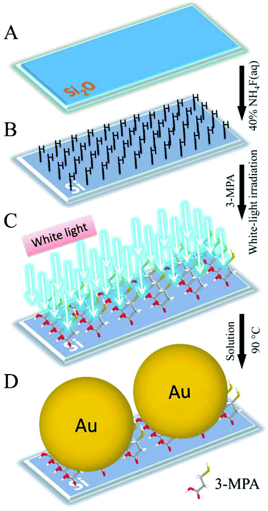 | ||
| Scheme 1 The strategy for grafting of a high-quality organic monolayer on a silicon surface to catalyze nanoparticle growth. From a cleaned Si(111) wafer (A), an atomically smooth Si(111)–H surface is made (B), which can be modified with 3-MPA molecules under white-light irradiation (C), and then catalyzes the growth of AuNPs on the surface (D). | ||
Experimental section
Equipment
White light used for the grafting reaction was generated using 125 W fluorescent work light. X-ray photoelectron spectroscopy (XPS) data were obtained on a PHI Quantum 2000 X-ray photoelectron spectrometer (P < 5 × 10⁻¹⁰ Torr) using monochromatic Al Kα radiation (10 kV) with a 200 μm spot. Scanning electron microscopy (SEM) images were obtained with a Hitachi S-4800 SEM (P < 10−8 Torr) with an accelerating voltage of 15 kV. The metallographic microscopy image was obtained with a Sunny MX6R upright metallurgical microscope. Silicon nitride (Si3N4) was deposited using a Thermco Nitride Low Pressure Chemical Vapor Deposition (LPCVD) system. A surface coating system G3 Spin Coater was used to spin coat the AZ5214E photoresist. A Karl Suss MA6 mask aligner was used to realize UV-lithography. The baking process was conducted with an IKA electric heating panel. An Alcatel AMS200 etcher with an optimized Deep Reactive Ion Etching (DRIE) system was used to conduct Inductively Coupled Plasma (ICP) Etching.Materials
Single-polished Si(111): n-type, Sb-doped, 450 ± 15μm thick, resistivity 0.01–0.02 Ω cm (Addison Engineering, CA). Ethanol (absolute), mesitylene (>99.5%), dichloromethane (>99.5%), potassium dicyanoaurate (99%), potassium citrate tribasic monohydrate (>99.5%), citric acid monohydrate (>99.5%), sulfuric acid (98%, AR), and hydrogen peroxide (30%, AR) were purchased from Sinopharm Chemical Reagent Co., Ltd (Shanghai, China). 3-Mercaptopropionic acid (99%), p-nitrothiophenol (>99.5%), and ammonium fluoride (40%, AR) were purchased from Aldrich.Preparation and functionalization of Si(111)–H
Si(111) wafers were cut into 1 × 1 cm2 pieces and cleaned in a piranha solution (H2SO4![[thin space (1/6-em)]](https://www.rsc.org/images/entities/char_2009.gif) :H2O2 = 3:1) at 90 °C for 1 h, subsequently etched by using 40% NH4F for 10 min, and dried with a stream of argon gas. The 3-MPA solution was flushed with Ar for 30 min before and for 30 min after putting the fresh Si(111)–H wafer into the solution, before the light was turned on. The grafting reaction was performed by irradiation of a wafer-containing 20% (vol.) solution of 3-MPA in mesitylene with white-light for 1 h under an Ar atmosphere. Afterwards, the surface was excessively rinsed with CH2Cl2 and EtOH, and dried with a stream of argon gas.
:H2O2 = 3:1) at 90 °C for 1 h, subsequently etched by using 40% NH4F for 10 min, and dried with a stream of argon gas. The 3-MPA solution was flushed with Ar for 30 min before and for 30 min after putting the fresh Si(111)–H wafer into the solution, before the light was turned on. The grafting reaction was performed by irradiation of a wafer-containing 20% (vol.) solution of 3-MPA in mesitylene with white-light for 1 h under an Ar atmosphere. Afterwards, the surface was excessively rinsed with CH2Cl2 and EtOH, and dried with a stream of argon gas.
In situ growth of AuNPs on the functionalized Si(111)–H surface
3-MPA-modified Si(111) wafers were put into a solution of KAu(CN)2 (2.5 mM/5 mM), potassium citrate (77 mM), citric acid (32 mM) and heated at 90 °C for 10 min/20 min. Then the wafers were excessively rinsed with ultrapure water and dried with a stream of argon gas.Process flow for fabricating a patterned chip
4 inch silicon wafer was soaked in a piranha solution (H2SO4:H2O2 = 3:1), rinsed with deionized water, and dried by nitrogen blowing. 100 nm silicon nitride was deposited by Low Pressure Chemical Vapor Deposition (LPCVD), and then the AZ5214E photoresist was spin-coated on the wafer at 2000 rpm for 30 s. After baking at 96 °C for 4 min, XMU patterns were generated by UV-lithography and developed. The wafer was further etched with SF6 by Inductively Coupled Plasma etching (ICP) to transfer the XMU pattern onto silicon nitride to expose the subjacent silicon surface. Finally the wafer was soaked in acetone to remove the photoresist. The patterned chip was operated in the procedure described above to construct the AuNP–Si system.
Raman experiment
All Raman spectra were recorded on an XploRA Raman System. The power at the sample location was 2.42 mW excited with a 638 nm laser line and the integration time was 20 s. The laser light was focused onto the sample using 50 × L objective lens (Leica microscope). p-Nitrothiophenol (p-NTP) was adsorbed onto the AuNP–Si surface by soaking in a 5 mM solution of ethanol for 30 min. The samples were then rinsed with ethanol, and left to dry in argon flow for 1 min before measurements.Results and discussion
Characterization of the functionalized Si(111)–H surface
After the formation of the Si(111)–H surface, the surface was functionalized by photografting of 3-MPA molecules at room temperature as detailed in Scheme 1 (step B→C). The modified surface was characterized using X-ray photoelectron spectroscopy (XPS) to obtain the binding energies of C, S, and Si elements. Fig. 1 shows the C1s, S2p and Si2p regions of the resulting XPS spectra of the 3-MPA-modified Si(111) surface (step C). By examining the C1s XPS spectrum, a major peak at 285.2 eV can be attributed to the –CH2–, which is consistent with recent studies.31–33 The shoulder peak at 286.1 eV can be attributed to the alcohol carbon (C–O) of the 3-MPA-modified Si(111).34,35 According to the XPS spectrum, we can estimate the atomic ratio of the two types of carbon to be nearly 2:1, corresponding to the theoretical ratio. As shown in Fig. 1b, the S2p XPS spectrum shows typical S peaks at 168.3 eV and 170.2 eV, fitted by a doublet of Voigt peaks with a fixed intensity ratio of S2p3/2:S2p1/2 = 2:1. This shows that the S–H bond is well maintained.36,37 The doublet peaks found at 99.8 and 100.6 eV are in good agreement with the Si2p3/2 and Si2p1/2 in the expected 2:1 area ratio (Fig. 1c). In particular, the silicon spectrum also displays a weak broad peak within the region of 102–105 eV. We assigned this peak to the formation of the Si–O bonds, which is consistent with a previous study.38,39
 | ||
| Fig. 1 X-ray photoelectron region spectra of a monolayer of 3-MPA grafted on a Si(111)–H surface prepared by the method of white-light irradiation, (a) C 1s, (b) S 2p, (c) Si 2p and (d) the analyzed grafted structure of 3-MPA on the Si(111)–H surface. | ||
The XPS data clearly demonstrate that 3-MPA molecules were grafted on the Si(111)–H surface via the C![[double bond, length as m-dash]](https://www.rsc.org/images/entities/char_e001.gif) O carboxyl group by forming Si–O–C bonds. The S–H bond of the 3-MPA molecule was well maintained after photografting on the Si(111)–H surface. To give an intuitive view, Fig. 1d shows the analyzed grafted structure of 3-MPA on the Si(111)–H surface.
O carboxyl group by forming Si–O–C bonds. The S–H bond of the 3-MPA molecule was well maintained after photografting on the Si(111)–H surface. To give an intuitive view, Fig. 1d shows the analyzed grafted structure of 3-MPA on the Si(111)–H surface.
AuNPs’ in situ growth
Fig. 2 shows the SEM images of AuNPs grown on 3-MPA-modified silicon surfaces under different conditions (step C→D in Scheme 1) and the size distribution correspondingly. It can be concluded that the grafted 3-MPA molecules successfully catalyze Au(CN)2− ions in the solution phase reduced into AuNPs on the Si(111) surface. The coverage of AuNPs increased with the concentration of Au(CN)2− and the treatment time. As shown in Fig. 2a, the AuNPs were approximately 10 nm in size. On doubling the treatment time, the particle size enlarged to 11 nm. The AuNPs would be 15 nm, if the concentration of Au(CN)2− in the solution phase was doubled. When we double the concentration of Au(CN)2− and the treatment time, the size of AuNPs would be enlarged to 21 nm. On this condition, as the 3-MPA-modified Si(111) wafers were placed into a solution of 5 mM KAu(CN)2 and heated at 90 °C for 20 min, the AuNPs grew in a closely packed manner on the modified surface, and there were few vacant spaces between these AuNPs. According to the statistical analysis, the size distribution of AuNPs is uniform, approximately 10, 11, 15, and 21 nm in diameter under various conditions. As mentioned before, only small nanoparticles with dimensions below 20 nm can efficiently generate hot electrons with large energies.16 Thus, it is meaningful that the packing and size of these small AuNPs can be, to a large extent, influenced by the concentration of Au(CN)2− and the treatment time. | ||
| Fig. 2 Scanning electron microscopy (SEM) images and the size distribution of AuNPs grown on 3-MPA-modified Si surfaces under different conditions. (a) SEM images of the AuNPs with a size of approximately 10 nm, and the corresponding size distribution. (b) SEM images of the AuNPs with a size of approximately 11 nm, and the corresponding size distribution. (c) SEM images of the AuNPs with a size of approximately 15 nm, and the corresponding size distribution. (d) SEM images of the AuNPs with a size of approximately 21 nm, and the corresponding size distribution. The electroless deposition solution contained KAu(CN)2, potassium citrate, and citric acid. The amounts of potassium citrate and citric acid were kept constant. (a) 2.5 mM KAu(CN)2, 10 min; (b) 2.5 mM KAu(CN)2, 20 min; (c) 5 mM KAu(CN)2, 10 min; (d) 5 mM KAu(CN)2, 20 min. | ||
It should be emphasized that AuNPs cannot be obtained from Au(CN)2− ions on either the cleaned Si(111) surface or the hydrogen-terminated Si(111) surface without molecular modification (see Fig. S1 in the ESI†). This further proves that the dense grafting of 3-MPA molecules onto the Si(111)–H surface is the key step to successfully catalyze Au(CN)2− ions reduced into AuNPs on the Si(111) surface. The whole mechanism of catalyzing AuNPs’ growth is inferred as follows: Au(CN)2− ions are first captured by the modified 3-MPA molecules on the silicon surface, and are superveniently reduced to atoms by the molecular functional groups (–S–H or Si–O–C(–R)–O–H). Several surface bonding atoms are aggregated into a crystal nucleus to catalyze the reduction process of Au(CN)2− ions in the surrounding solution by the reducing agents (potassium citrate and citric acid). As the reaction proceeds in an elevated temperature, the initial nucleation sites can grow rapidly to form AuNPs on the Si surface in a few minutes.
The AuNPs can grow selectively in a certain region on a patterned chip. A patterned chip was fabricated by the process flow provided in the ESI† (Fig. S2). Fig. 3 shows the metallographic microscopy image of the patterned Si–Si3N4 chip and SEM images of the chip after the treatment according to Scheme 1. It can be seen that the method detailed in Scheme 1 produces selective growth of AuNPs on the patterned chip. Specifically, the AuNPs could not be grown on a silicon nitride (Si3N4) surface, but were grown well on the exposed Si(111)–H surface modified with 3-MPA. Moreover, we also found that these AuNPs did not detach from the prepared surface even when the sample was sonicated in mesitylene, indicating that the AuNPs were firmly bonded to the Si(111) surface. Therefore, it is clear from these results that in situ growth of small sized AuNPs on the silicon-based devices can be certainly realized using the reported method.
 | ||
| Fig. 3 Metallographic microscopy image (a) and SEM images (b), (c) of a patterned Si–Si3N4 chip; AuNPs grew selectively on the Si region using the method detailed in Scheme 1. (a) The pink areas (XMU) are the constructed AuNP–molecule–Si system and the dark green area is silicon nitride (Si3N4). The 3-MPA-modified Si(111) patterned chip was put into an electroless deposition solution containing KAu(CN)2 (5 mM), potassium citrate (77 mM) and citric acid (32 mM) for 20 min to obtain AuNPs. | ||
Surface-enhanced Raman scattering (SERS) enhancement of the AuNP–Si substrate
Since the AuNPs grew selectively on the patterned Si–Si3N4 chip in a closely packed manner, it is very interesting to evaluate its SERS enhancement,40,41 and p-NTP was used as the probe.42Fig. 4 shows the SERS spectrum of 5 × 10⁻⁴ M p-NTP molecules adsorbed on the constructed AuNP–Si substrate and the spectrum of the substrate. The observed Raman bands that are assigned to p-NTP include ring stretching mode at 1572 cm−1, symmetric stretching mode of the nitro group at 1336 cm−1, C–H bending mode at 1110 cm−1, and C–S stretching mode at 1080 cm−1.43 A minor background signal from the substrate marked in red can also be observed in the SERS spectrum. The marked band around 916–1005 cm−1 is attributed to the silicon bulk as observed in spectrum (b). The Raman peaks of p-NTP molecules are so prominent that the background signal is negligible. | ||
| Fig. 4 (a) SERS spectrum of p-nitrothiophenol (p-NTP) on the AuNP–Si substrate. (b) The Raman spectrum of the constructed AuNP–Si substrate. The 3-MPA-modified Si(111) chip was put into an electroless deposition solution containing KAu(CN)2 (5 mM), potassium citrate (77 mM) and citric acid (32 mM) for 20 min to obtain AuNPs. | ||
Theoretical simulation
Since the photografting of 3-MPA molecules onto the Si(111)–H surface is a key step for subsequence, it is meaningful to further understand the addition reaction of 3-MPA molecules with the Si(111)–H surface under white-light irradiation.The reaction pathway for this process is proposed in Fig. 5. Under white light irradiation, some special localized electron [e−]/hole [h+] pairs are activated on the Si(111)–H surface. The surface sites with the positive charge population may be attacked by the carbonyl π-electrons to form the Si–O bond. Meanwhile, the hydrogen atom attacks the carbon atom of the carbonyl group to form the C–H bond. DFT calculations were conducted to verify the rationale of the proposed reaction mechanism. The cluster model Si24H36 was used to mimic the hydrogenated silicon surface, reproducing a portion of the Si(111)–H surface. In the cluster model, hydrogen atoms were used to terminate the dangling bonds due to the surface silicon atoms (twelve nearest-neighbor on-top reaction sites). This condition also satisfied the tetrahedral sp3 bonding environment of the silicon atoms. DFT calculations with the B3LYP functional44–46 combined with the 6-311+G** full-electron basis set were performed using the Gaussian 09 package.47
 | ||
| Fig. 5 Proposed mechanism of white-light initiated 3-MPA grafting on the hydrogen-terminated Si(111) surface. | ||
Fig. 6 presents the reaction potential energy surfaces for the singlet ground state (S0, bottom) and the first singlet excited state (S1, top). The ground state reaction path was first determined by finding the minima and the saddle points corresponding to the reactants, transition state (TS) and product on the potential energy curve (PEC). Full optimization without any geometry constraints was performed in DFT calculations. Vibrational frequency analysis was performed to confirm the right intermediates and transition state along the reaction coordinate. The first vibrational frequency values of the reactants, transition state and product are predicted to be 2.6, 806.5i and 9.2 cm−1, respectively. Geometrical parameters of relevant states have been provided in the ESI† (Table S1–4).
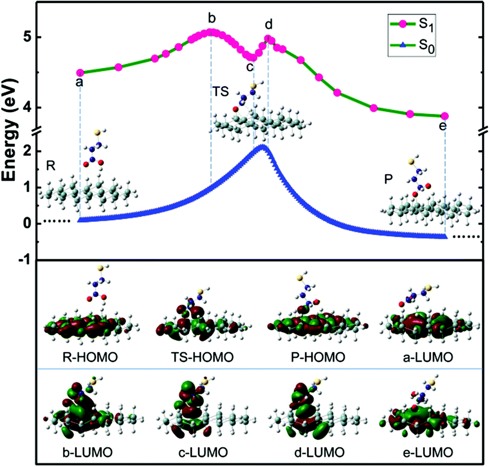 | ||
| Fig. 6 Calculated reaction paths for the addition of 3-MPA to the Si24H36 cluster. The energies were calculated at the ground state S0 and the first excited state S1. The inserted images correspond to the optimized structures of the reactants, transition state, and product on the potential energy curve in the ground state S0. The images in the bottom show the highest occupied molecular orbital (HOMO) of R, TS and P on the S0 PEC, and the lowest unoccupied molecular orbital (LUMO) of some marked points along the reaction coordinate. | ||
Table S5† gives the calculated natural bonding orbital (NBO) charge for the transition state (TS) on the potential energy curve in the S0 state, revealing the negatively charged hydrogen atom and the positively charged silicon atom in the four-member ring. For the S0 state, the heat of reaction and the activation barrier energy are −0.36 eV and 2.10 eV, respectively. This indicates that the grafted reaction is kinetically disadvantageous due to the large activation energy barrier. The data show that in S0 the reaction presents a very small heat of reaction and a huge activation barrier, confirming the implausibility of thermal activation for this process. Consequently, the grafting of 3-MPA as a photochemical reaction became the focus of our attention.
To explore the influence of light, the potential energy curve of the first singlet existed state (S1) was calculated using the time-dependent DFT approach (TD-B3LYP) along the reaction coordinate at the S0 state. Geometry optimization and frequency calculations were not performed to examine the nature of the S1 state potential surface in the vicinity of a, b, c, d and e geometries in the S0 state. As the probe molecule and the cluster model are so large, we employ the TD-DFT calculation to estimate the reaction possibility qualitatively based on the geometries along the reaction path in the ground states on the basis of a vertical approximation. Since the gap between valence and conduction bands of the Si(111)–H surface is experimentally measured to be about 1.1–1.3 eV,32 visible light can excite the hydrogen-terminated silicon. To reduce the computational cost, the silicon surface was modeled as a single-layer Si24H36 cluster. As the optical gap has high dependence on the size of the cluster,48–50 the transition energy is larger than the experimental values, similar to many previous theoretical studies (Table 1).32,51
| S0 | S1 | ||
|---|---|---|---|
| R | 0 | A | 4.49 |
| TS | 2.10 | B | 5.07 |
| P | −0.36 | C | 4.71 |
| — | — | D | 4.98 |
| — | — | E | 3.87 |
By considering the absorption of white light, the reaction can be activated with a sharp decline of the energy barrier in singlet excited states. Our TD-B3LYP results show that at the S1 PEC,51–53 a new intermediate can be formed, where the two reaction barriers decrease significantly to 0.58 eV and 0.27 eV compared with 2.10 eV of the S0. Fig. 6 also shows the electron cloud distribution changes accordingly along the reaction coordinate at the potential energy surface of the S0 state. For the reactants (R), the HOMO mainly displays a population on the Si atoms, while for the product (P) it partially populates in the grafted 3-MPA. The TS is a four-member-ring configuration that is unstable due to the large ring tension. The electron cloud of the TS also shows that there is a weak bonding interaction between the adsorbate and the Si24H36 cluster. Thus the activation energy barrier in the S0 PEC is relatively high. By contrast, when the reactants absorbed photonic energy, they were excited to the S1 state with a large oscillator strength (f = 0.033). Then the excited reactants can readily surmount a lower energy barrier of 0.58 eV to form a new four-member-ring intermediate, which is relatively stable due to the π* bonding effect localized in the ring (see electron cloud distribution c-LUMO in Fig. 6). The intermediate can easily surmount the lower energy barrier of 0.27 eV to be transformed to the excited product, in which there exists a strong σ bonding with the Si–O bond. Furthermore, the Gibbs free energy of the product is around 0.62 eV lower than that of reactants in the S1 state. The product then returns to the S0 state of the final product.
Our calculations showed that the additional reaction mechanism follows some special localized electron [e−]/hole [h+] pairs activated on the Si(111)–H surface induced by white light. The surface sites with the positive charge population are attacked by the carbonyl π-electrons to form the Si–O bond. Meanwhile, the negatively charged hydrogen atom attacks the carbon atom of the carbonyl group to form the C–H bond. Our results of DFT calculations are undoubtedly very helpful to understand the photochemical mechanism for photografting of organic molecules on semiconductor surfaces.
Conclusions
In summary, we designed a novel, mild and effective method for grafting of high-quality organic monolayers on the silicon surface to catalyze small nanoparticles’ growth. By using a white light source, 3-MPA molecules were attached to the Si(111)–H surface at room temperature. XPS results confirmed the formation of the grafted Si–O bonds on the 3-MPA-modified Si(111) surfaces. The AuNPs grown on this functionalized surface have high uniformity and compactness. Our experiments have also demonstrated that AuNPs can grow selectively in a certain region on a patterned Si–Si3N4 chip. The high-density gold nanoparticle substrate with good reproducibility of the surface-enhanced Raman signal can serve as molecular detectors.The 3-MPA molecules grafted onto the Si(111)–H surface is the key step in the successful catalysis of AuNPs’ in situ growth. To understand the mechanism of the photografting of 3-MPA on the Si(111)–H surface better, DFT calculations were performed and the theoretical results indicated that the formation of the Si–O bond occurred at the PEC of the S1 state with a very low activation barrier about 30% of the ground state (S0) value. The reported strategy can be applied to the design of high-performance electronic/photonic devices by combining the synthetic advantages of the small size of AuNPs and silicon as well as the controllable functional versatility of the molecules.
Acknowledgements
This work was supported by the National Science Foundation of China (NSFC) (no. 21373172), the Innovation Group of Interfacial Electrochemistry (no. 21321062), MOST (no. 2011YQ03012400), and National Key Basic Research Program of China (2015CB932303).Notes and references
- D. H. Wan, H. L. Chen, T. C. Tseng, C. Y. Fang, Y. S. Lai and F. Y. Yeh, Adv. Funct. Mater., 2010, 20, 3064–3075 CrossRef CAS PubMed.
- M. Losurdo, M. M. Giangregorio, G. V. Bianco, A. Sacchetti, P. Capezzuto and G. Bruno, Sol. Energy Mater. Sol. Cells, 2009, 93, 1749–1754 CrossRef CAS PubMed.
- D. Hojo, T. Togashi, D. Iwasa, T. Arita, K. Minami, S. Takami and T. Adschiri, Chem. Mater., 2010, 22, 1862–1869 CrossRef CAS.
- O. Yaffe, L. Scheres, S. R. Puniredd, N. Stein, A. Biller, R. H. Lavan, H. Shpaisman, H. Zuilhof, H. Haick, D. Cahen and A. Vilan, Nano Lett., 2009, 9, 2390–2394 CrossRef CAS PubMed.
- M. W. Knight, H. Sobhani, P. Nordlander and N. J. Halas, Science, 2011, 332, 702–704 CrossRef CAS PubMed.
- M. Grätzel, Nature, 2001, 414, 338–344 CrossRef PubMed.
- S. M. Sze and K. K. Ng, Physics of semiconductor devices, John Wiley & Sons, 2006 Search PubMed.
- H. A. Atwater and A. Polman, Nat. Mater., 2010, 9, 205–213 CrossRef CAS PubMed.
- R. Elghanian, J. J. Storhoff, R. C. Mucic, R. L. Letsinger and C. A. Mirkin, Science, 1997, 277, 1078–1081 CrossRef CAS.
- C. L. Nehl, H. W. Liao and J. H. Hafner, Nano Lett., 2006, 6, 683–688 CrossRef CAS PubMed.
- G. Raschke, S. Kowarik, T. Franzl, C. Sonnichsen, T. A. Klar, J. Feldmann, A. Nichtl and K. Kurzinger, Nano Lett., 2003, 3, 935–938 CrossRef CAS.
- Y. W. C. Cao, R. C. Jin and C. A. Mirkin, Science, 2002, 297, 1536–1540 CrossRef CAS PubMed.
- J. A. Schuller, E. S. Barnard, W. Cai, Y. C. Jun, J. S. White and M. L. Brongersma, Nat. Mater., 2010, 9, 193–204 CrossRef CAS PubMed.
- S. Mukherjee, F. Libisch, N. Large, O. Neumann, L. V. Brown, J. Cheng, J. B. Lassiter, E. A. Carter, P. Nordlander and N. J. Halas, Nano Lett., 2012, 13, 240–247 CrossRef PubMed.
- I. Thomann, B. A. Pinaud, Z. Chen, B. M. Clemens, T. F. Jaramillo and M. L. Brongersma, Nano Lett., 2011, 11, 3440–3446 CrossRef CAS PubMed.
- A. O. Govorov, H. Zhang and Y. K. Gun'ko, J. Phys. Chem. C, 2013, 117, 16616–16631 CAS.
- M. T. Sheldon, J. van de Groep, A. M. Brown, A. Polman and H. A. Atwater, Science, 2014, 346, 828–831 CrossRef CAS PubMed.
- J. M. Buriak, Chem. Rev., 2002, 102, 1271–1308 CrossRef CAS PubMed.
- S. Ciampi, J. B. Harper and J. J. Gooding, Chem. Soc. Rev., 2010, 39, 2158–2183 RSC.
- H. Sugimura, S. H. Mo, K. Yamashiro, T. Ichii and K. Murase, J. Phys. Chem. C, 2013, 117, 2480–2485 CAS.
- Y. J. Song, Y. Wang, B. B. Li, C. Fernandes and H. E. Ruda, Nanoscale, 2013, 5, 6779–6789 RSC.
- Y. J. Song, Z. S. Zhang, H. E. Elsayed-Ali, H. N. Wang, L. L. Henry, Q. Q. Wang, S. L. Zou and T. Zhang, Nanoscale, 2011, 3, 31–44 RSC.
- Y. J. Song, W. T. Yin, Y. H. Wang, J. P. Zhang, Y. Wang, R. M. Wang, J. B. Han, W. Wang, S. V. Nair and H. E. Ruda, Sci. Rep., 2014, 4, 4991 CAS.
- P. E. Colavita, B. Sun, K. Y. Tse and R. J. Hamers, J. Am. Chem. Soc., 2007, 129, 13554–13565 CrossRef CAS PubMed.
- B. J. Eves, Q. Y. Sun, G. P. Lopinski and H. Zuilhof, J. Am. Chem. Soc., 2004, 126, 14318–14319 CrossRef CAS PubMed.
- R. Boukherroub and D. D. M. Wayner, J. Am. Chem. Soc., 1999, 121, 11513–11515 CrossRef CAS.
- T. Hentschel, D. Isheim, R. Kirchheim, F. Muller and H. Kreye, Acta Mater., 2000, 48, 933–941 CrossRef CAS.
- Y. He, Y. L. Zhong, F. Peng, X. P. Wei, Y. Y. Su, S. Su, W. Gu, L. S. Liao and S. T. Lee, Angew. Chem., Int. Ed., 2011, 50, 3080–3083 CrossRef CAS PubMed.
- X. M. Shen, Y. J. Song, S. Li, R. S. Li, S. X. Ji, Q. Li, H. P. Duan, R. W. Xu, W. T. Yang, K. Zhao, R. Rong and X. Y. Wang, RSC Adv., 2014, 4, 34179–34188 RSC.
- L. A. Huck and J. M. Buriak, J. Am. Chem. Soc., 2012, 134, 489–497 CrossRef CAS PubMed.
- P. Bertani, X. J. Wen and W. Lu, J. Electron. Mater., 2012, 41, 830–836 CrossRef CAS PubMed.
- X. Y. Wang, R. E. Ruther, J. A. Streifer and R. J. Hamers, J. Am. Chem. Soc., 2010, 132, 4048–4049 CrossRef CAS PubMed.
- Y. L. Zhong and S. L. Bernasek, J. Am. Chem. Soc., 2011, 133, 8118–8121 CrossRef CAS PubMed.
- C. K. Chan, R. Ruffo, S. S. Hong and Y. Cui, J. Power Sources, 2009, 189, 1132–1140 CrossRef CAS PubMed.
- Q. Y. Sun, L. de Smet, B. van Lagen, A. Wright, H. Zuilhof and E. J. R. Sudholter, Angew. Chem., Int. Ed., 2004, 43, 1352–1355 CrossRef CAS PubMed.
- Y. H. Lai, C. T. Yeh, C. C. Yeh and W. H. Hung, J. Phys. Chem. B, 2003, 107, 9351–9356 CrossRef CAS.
- T. Ishida, N. Choi, W. Mizutani, H. Tokumoto, I. Kojima, H. Azehara, H. Hokari, U. Akiba and M. Fujihira, Langmuir, 1999, 15, 6799–6806 CrossRef CAS.
- A. Bansal, X. L. Li, I. Lauermann, N. S. Lewis, S. I. Yi and W. H. Weinberg, J. Am. Chem. Soc., 1996, 118, 7225–7226 CrossRef CAS.
- R. Miao, L. X. Mu, H. Y. Zhang, H. T. Xu, B. J. Zhou, G. W. She, P. F. Wang and W. S. Shi, ACS Appl. Mater. Interfaces, 2013, 5, 1741–1746 CAS.
- O. Bisi, S. Ossicini and L. Pavesi, Surf. Sci. Rep., 2000, 38, 1–126 CrossRef CAS.
- J. H. Park, L. Gu, G. von Maltzahn, E. Ruoslahti, S. N. Bhatia and M. J. Sailor, Nat. Mater., 2009, 8, 331–336 CrossRef CAS PubMed.
- H. Foll, M. Christophersen, J. Carstensen and G. Hasse, Mater. Sci.Eng., R, 2002, 39, 93–141 CrossRef.
- B. Skadtchenko and R. Aroca, Spectrochim. Acta, Part A, 2001, 57, 1009–1016 CrossRef.
- A. D. Becke, Phys. Rev. A, 1988, 38, 3098–3100 CrossRef CAS.
- A. D. Becke, J. Chem. Phys., 1993, 98, 5648–5652 CrossRef CAS PubMed.
- C. T. Lee, W. T. Yang and R. G. Parr, Phys. Rev. B: Condens. Matter, 1988, 37, 785–789, DOI:10.1103/PhysRevB.37.785.
- M. J. Frisch, G. W. Trucks, H. B. Schlegel, G. E. Scuseria, M. A. Robb, J. R. Cheeseman, G. Scalmani, V. Barone, B. Mennucci and G. A. Petersson, et al., Gaussian 09, Revision A.02, Gaussian, Inc., Wallingford, CT, USA, 2009 Search PubMed.
- C. J. Barrelet, D. B. Robinson, J. Cheng, T. P. Hunt, C. F. Quate and C. E. D. Chidsey, Langmuir, 2001, 17, 3460–3465 CrossRef CAS.
- T. Vondrak and X. Y. Zhu, Phys. Rev. Lett., 1999, 82, 1967–1970 CrossRef CAS.
- F. Effenberger, G. Gotz, B. Bidlingmaier and M. Wezstein, Angew. Chem., Int. Ed., 1998, 37, 2462–2464 CrossRef CAS.
- M. Cossi, A. Boccia, A. G. Marrani and R. Zanoni, J. Phys. Chem. C, 2011, 115, 19210–19215 CAS.
- Y. Kanai and A. Selloni, J. Am. Chem. Soc., 2006, 128, 3892–3893 CrossRef CAS PubMed.
- A. Puzder, A. J. Williamson, J. C. Grossman and G. Galli, Phys. Rev. Lett., 2002, 88, 097401 CrossRef.
Footnote |
| † Electronic supplementary information (ESI) available: SEM images of the cleaned Si(111) surface or the Si(111)–H surface without molecule modification after being immersed in an electroless deposition solution; schematic plots for fabricating a patterned chip; and the calculated parameters with the DFT method at the B3LYP/6-311+G** level. See DOI: 10.1039/c5nr00664c |
| This journal is © The Royal Society of Chemistry 2015 |