
 Open Access Article
 This Open Access Article is licensed under a Creative Commons Attribution-Non Commercial 3.0 Unported Licence
Core–shell InGaN/GaN nanowire light emitting diodes analyzed by electron beam induced current microscopy and cathodoluminescence mapping†
M.
Tchernycheva
*a,
V.
Neplokh
a,
H.
Zhang
a,
P.
Lavenus
a,
L.
Rigutti
ab,
F.
Bayle
a,
F. H.
Julien
a,
A.
Babichev
acd,
G.
Jacopin
e,
L.
Largeau
f,
R.
Ciechonski
g,
G.
Vescovi
g and
O.
Kryliouk
h
aInstitut d'Electronique Fondamentale, UMR 8622 CNRS, University Paris Sud, 91405 Orsay cedex, France. E-mail: maria.tchernycheva@u-psud.fr
bGroupe de Physique des Matériaux, UMR CNRS 6634, University and INSA of Rouen, Normandie University, 76800 St. Etienne du Rouvray, France
cITMO University, 197101 St. Petersburg, Russia
dIoffe Institute, 194021 St. Petersburg, Russia
eICMP LOEQ Ecole Polytechnique Fédérale de Lausanne, 1015 Lausanne, Switzerland
fLPN-CNRS, Route de Nozay, 91460 Marcoussis, France
gGLO AB, Ideon Science Park, Scheelevägen 17, S-223 70 Lund, Sweden
hGLO-USA, 1225 Bordeaux Dr, Sunnyvale, CA 94086, USA
First published on 15th June 2015
Abstract
We report on the electron beam induced current (EBIC) microscopy and cathodoluminescence (CL) characterization correlated with compositional analysis of light emitting diodes based on core/shell InGaN/GaN nanowire arrays. The EBIC mapping of cleaved fully operational devices allows to probe the electrical properties of the active region with a nanoscale resolution. In particular, the electrical activity of the p–n junction on the m-planes and on the semi-polar planes of individual nanowires is assessed in top view and cross-sectional geometries. The EBIC maps combined with CL characterization demonstrate the impact of the compositional gradients along the wire axis on the electrical and optical signals: the reduction of the EBIC signal toward the nanowire top is accompanied by an increase of the CL intensity. This effect is interpreted as a consequence of the In and Al gradients in the quantum well and in the electron blocking layer, which influence the carrier extraction efficiency. The interface between the nanowire core and the radially grown layer is shown to produce in some cases a transitory EBIC signal. This observation is explained by the presence of charged traps at this interface, which can be saturated by electron irradiation.
Introduction
Electron Beam Induced Current (EBIC) microscopy has been widely used to characterize optoelectronic devices for more than thirty years.1 In particular, nitride light emitting diodes (LEDs) in the form of two-dimensional (2D) films have been intensively investigated by this technique.2,3 In 2D LEDs, EBIC was used to probe the electrical activity of the device with a high resolution and to detect failures induced by material defects.3–5Recently semiconductor nanowires have emerged as a way to boost the performance of nitride LEDs by improving the material quality.6,7 The photon re-absorption effect can take place in core/shell nanowire LEDs. However, it has been theoretically shown that in the case of photon recycling, the nanowire LEDs can successfully compete with planar LEDs at high currents.8 In addition, core/shell structures show promise to reduce the efficiency droop by increasing the active area of the LED and getting rid of the quantum confined Stark effect.6,7 However, the replacement of a 2D active region by 3D nanowires increases the complexity of the device structure and impacts its electrical and optical behavior.
Today there is a strong regain of interest for EBIC microscopy applied to optoelectronic devices with a nanostructured active region. Indeed, for nanostructured materials standard macroscopic characterization techniques provide only average values of important parameters, which is not sufficient for in-depth understanding of the device operation. On the contrary, EBIC offers excellent spatial resolution and allows to address individual nanostructures composing the macroscopic device.9–15 In particular, EBIC microscopy is a perfectly dedicated tool to investigate the structural and the electrical properties of the three-dimensional nanostructured LEDs.
In the past years, several EBIC investigations of single nanowires and nanowire devices built of different materials have been reported,9–21 sometimes coupled with cathodoluminescence (CL) mapping.10,21 Regarding nitride nanowires, in our previous work we have addressed the parallel transport properties of core–shell InGaN/GaN single wire LEDs.20 Recently, Tchoulfian et al. have proposed a cross-sectional approach based on cleaving core/shell nanowires along their axis, which has been applied to GaN p–n junction core–shell nanowires.14 However no cross-sectional studies of full nanowire LEDs has ever been reported. In addition, no correlation between induced current and optical mapping has ever been performed on core/shell nanowires. Since the LED operation implies both the electrical transport and the optical recombination, the analysis of both electrical and optical properties and their correlation with material parameters is necessary to understand and improve the device performance.
In this work we apply an original approach correlating EBIC and CL microscopies with compositional analysis to assess the material, electrical and optical properties of industrial-grade LEDs based on InGaN/GaN core–shell nanowires. Individual nanowires from fully operational macroscopic LEDs are probed by EBIC under both top-view and cross-sectional imaging configurations. The electrical activity of the p–n junction on the m-planes and on the semi-polar planes is assessed. In particular, the suppression of the electrical activity at the semi-polar planes is demonstrated. EBIC and CL maps of the nanowire cross-section show no signal dips, which confirms the absence of electrically active defects crossing the active region. EBIC profiles perpendicular to the wire elongated direction at different positions demonstrate a good homogeneity of the material parameters of GaN (doping concentrations and minority carrier diffusion lengths) along the wire axis. Coupled EBIC and CL characterizations on cleaved nanowires demonstrate the correlation between the electrical and optical signals: the reduction of the EBIC signal toward the nanowire top is accompanied by an increase of the CL intensity. This effect is interpreted as a consequence of the In and Al gradients in the quantum well and in the electron blocking layer evidenced by energy-dispersive X-ray spectroscopy (EDX), which influence the carrier extraction efficiency. Finally, current maps of several cleaved nanowires reveal the presence of a transitory EBIC signal localized at the interface between the n-doped nanowire core and the radially grown n-doped underlayer. This signal disappears under electron beam irradiation and a standard EBIC map with a signal originating from the radial p–n junction is recovered. The origin of the unexpected EBIC signal from the core/underlayer interface is attributed to charged traps creating local potential maxima, which can be saturated by electron beam irradiation.
Results and discussion
Sample structure
The vertical InGaN/GaN core–shell nanowires have been formed on an n-type GaN/sapphire template by selective area growth by MOVPE using a SiN dielectric mask with sub-micrometer openings. The nanowire structure is schematized in Fig. 1(a). First n-doped (∼1 × 1019 cm−3) GaN core of a diameter ∼200–250 nm is formed. It is laterally overgrown with a 200 nm thick n-doped (∼5 × 1018 cm−3) GaN underlayer. Then the active region containing one 7 nm thick InGaN quantum well with 12–16% In content and an AlGaN electron blocking layer is deposited. Finally, a 150 nm thick p-doped GaN shell is grown with a Mg concentration of ∼5 × 1019 cm−3. (The doping levels were calibrated on 2D layers. However, it should be noted that the doping levels in nanowires may significantly differ from the ones in equivalent planar structures, due to the surface segregation and other effects.22,23) The growth is terminated with a p+-doped GaN surface layer. The LED nanowires consist of a cylindrical part having a hexagonal cross-section with lateral facets defined by m-planes and of a top pyramidal part defined by semipolar (10![[thin space (1/6-em)]](https://www.rsc.org/images/entities/char_2009.gif) −11) planes. The material deposition on the top semipolar planes has been minimized by adjusting the growth conditions.21 As shown in ESI Fig. S1b,† the InGaN quantum well is absent on the semipolar planes and the p-doped shell thickness is strongly reduced. In the following we will come back to this point and probe the electrical activity of the semipolar planes by direct EBIC imaging.
−11) planes. The material deposition on the top semipolar planes has been minimized by adjusting the growth conditions.21 As shown in ESI Fig. S1b,† the InGaN quantum well is absent on the semipolar planes and the p-doped shell thickness is strongly reduced. In the following we will come back to this point and probe the electrical activity of the semipolar planes by direct EBIC imaging.
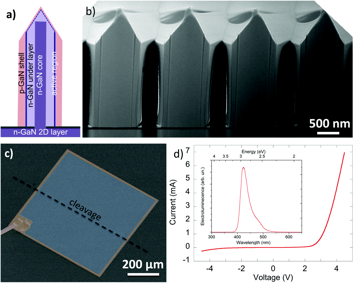 | ||
| Fig. 1 (a) Schematic of the nanowire structure. (b) Cross-sectional STEM image (electron beam is parallel to the <1 − 210> direction). (c) SEM image in artificial colors of a processed 700 × 700 μm2 mesa LED. The dashed line illustrates the device cleavage for cross-sectional EBIC measurements. (d) I–V curve of the 300 × 300 μm2 LED. Inset shows the EL spectrum for 1.8 A cm−2 electrical injection. | ||
Nanowire structural properties have been studied by transmission electron microscopy. A lamella was prepared by Focused Ion Beam cutting and lift-out technique using Pt capping and soldering. Fig. 1(b) shows a scanning transmission electron microscopy (STEM) image for (1 − 210) zone axis (i.e. the image plane is perpendicular to the nanowire m-plane facets). The InGaN quantum well thickness is found to be 6.5 ± 1 nm. EDX mapping within the STEM (Fig. 1Sd†) shows the presence of compositional gradients in the quantum well and in the electron blocking layer. The In (Al) content in the quantum well (electron blocking layer) varies from 13.5 ± 1.5% (9 ± 1.5%) in the base part up to 18.5 ± 1.5% (19 ± 1.5%) in the top part. The compositional gradients along the m-planes induced by the surface kinetic difference of the deposited species have previously been evidenced by CL measurements in this type of nanowires.21,24
Nanowire arrays have been processed into square mesa LEDs shown in Fig. 1(c) with a typical size varying from 300 × 300 μm2 up to 3 × 3 mm2. The nanowire cores are contacted using the n-doped bottom 2D GaN layer. The nanowires outside the mesas are etched by inductively coupled plasma using Cl2/Ar chemistry. The bottom contact to the 2D GaN layer is defined by Ti/Al/Ti/Au metallization. The top mesa surface is covered with 200 nm ITO layer conformely deposited onto the nanowires using sputtering deposition and a lift-off. The central part of the mesa is left open while the perimeter is metallized as illustrated in Fig. 1(c). Fig. 1(d) shows an example of the 300 × 300 μm2 LED I–V curve. The device presents a rectifying behavior typical of a diode. The reverse leakage current (which is below 10−2 A cm−2 at −1 V reverse bias) may be attributed to the deep level state contribution.25 The electroluminescence spectrum collected under 1.8 A cm−2 injection is shown in the inset of Fig. 1(d). The room temperature emission is peaked at 420 nm with a shoulder at 490 nm. These two spectral contributions are attributed to the m-plane quantum well emission and to the emission from the In-rich region in the quantum well at the m-plane/semipolar plane junction as discussed in.21 In the following, we focus on the investigation of the electrical and optical properties of the nanowire LEDs using charge collection scanning electron microscopy and CL microscopy. Further details concerning the electroluminescence characterization of this kind of devices can be found in ref. 21.
The EBIC maps were measured at room temperature in a Hitachi SU8000 SEM controlled by a Gatan DigiScan system as described in ref. 20. The metallic pads of the device under test were contacted using micromanipulators connected to a low-noise current preamplifier SR570. All measurements were performed at zero bias. The beam current arriving at the sample surface measured using a Faraday cup on the sample holder was between 0.4 and 0.9 nA. In the following analyses, all current maps are traced in normalized units, the measured maximal current being in the 10−8–10−7 A range.
Top-view characterization
First, the electrical activity of the semipolar planes has been probed in the top view configuration. EBIC maps have been recorded by scanning the top LED surface with the electron beam directed perpendicular to the substrate surface. Because of a strong attenuation of the electron beam in the ITO layer, the EBIC signal could only be recorded at high acceleration voltage (Vacc above 20 kV). For such high acceleration voltages the lateral resolution of the maps is rather poor (in the micrometer range) because of the large excitation volume. To improve the resolution, a dedicated sample with reduced ITO thickness was processed. The ITO thickness on the semipolar facets was measured by simultaneously depositing the ITO on a Si wafer fixed on a 60° tilted holder to imitate the inclination angle of the semipolar facets, which was then cleaved and observed in SEM. The ITO thickness was found to be 120 nm. The LED sample with reduced ITO thickness was used to analyze the details of the EBIC signal from semipolar facets using an acceleration voltage of 10 kV and impinging current of 0.9 nA as shown in Fig. 2(a) and (b). A strong EBIC signal is observed on the circumference of the wire corresponding to the radial p–n junction on the vertical facets. However, the EBIC signal drops to the background noise level when the excitation position approaches the nanowire center as seen from Fig. 2(b) and from the EBIC profile of Fig. 2(e).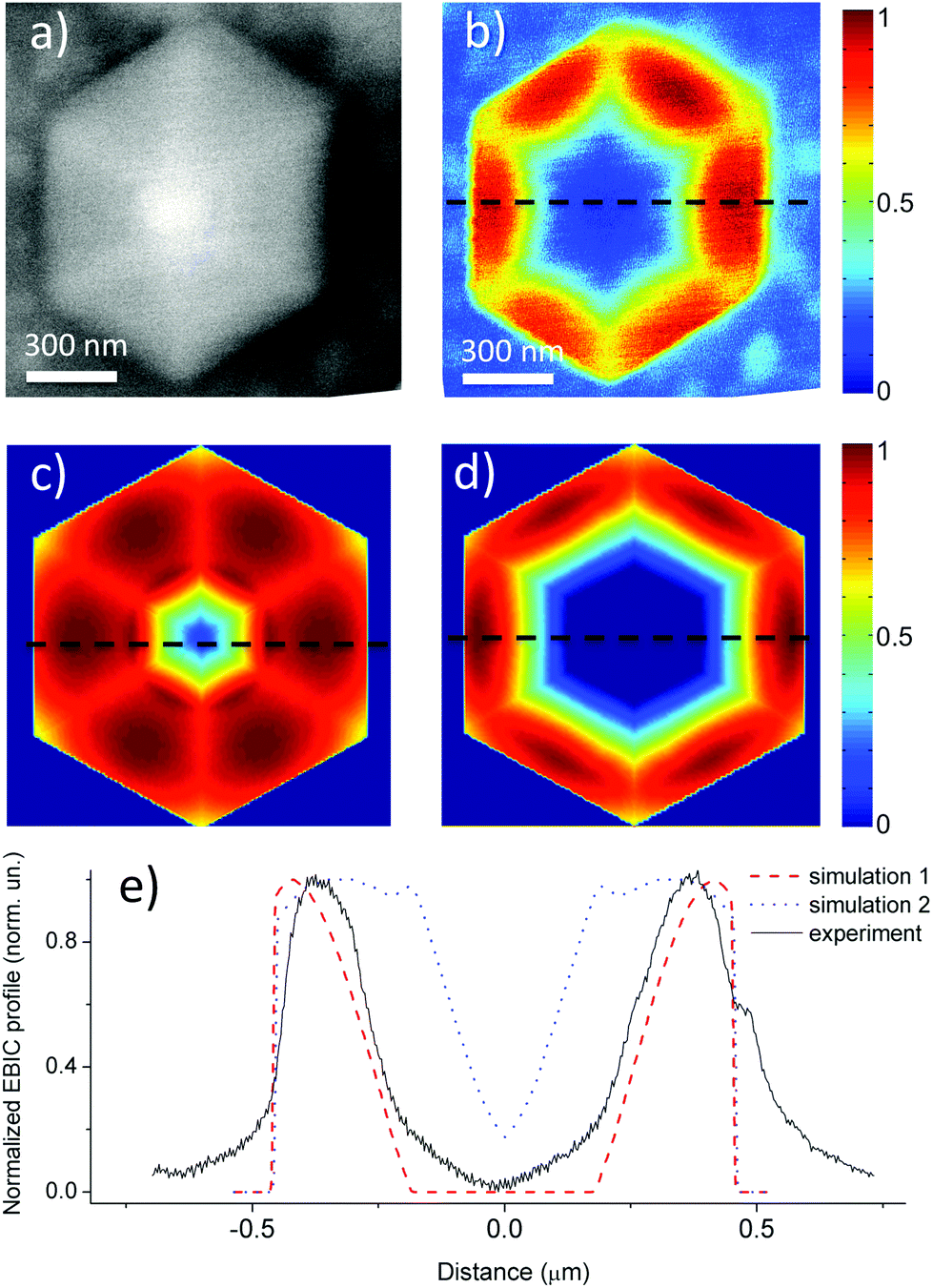 | ||
| Fig. 2 (a) Top-view SEM image and (b) corresponding normalized EBIC map collected from the LED sample with 120 nm ITO thickness. (c) Simulated EBIC map considering a homogeneous p–n junction on the semi-polar facets. (d) Simulated EBIC map considering that p–n junction is absent over the upper 2/3 of the semi-polar facets. (e) Experimental (full curve) and simulated normalized EBIC profiles cutting the wire perpendicular to the m-planes along the dashed lines in panels (b)–(d). The dotted curve corresponds to the map of panel (c) and the dashed curve corresponds to the map of panel (d). | ||
To analyze the origin of the EBIC signal, the electron beam – matter interaction has been analyzed by Monte-Carlo simulation using “Casino” software.26 We define the penetration depth as the distance corresponding to the maximum of the statistical distribution of the depths reached by incident electrons divided by e = 2.718. The penetration depth at Vacc = 10 kV on a facet tilted by 60° with respect to normal incidence is calculated to be 360 nm. The lateral extension of the excitation volume is of the same order of magnitude. Therefore, a contribution of the radial p–n junction on the m-planes is expected when the beam is placed close to the wire circumference. However only the semipolar planes should contribute to the EBIC signal when the beam excites the nanowire tip. The EBIC map has been modeled in a simple geometrical approximation assuming that the excitation is produced in a spherical volume. Different diameters have been considered. The details of the model can be found in the ESI.†Fig. 2(c) and (d) present the calculated EBIC map for excitation volume diameter of 400 nm under different assumptions regarding the extension of a p–n junction on the semipolar planes. Fig. 2(e) shows the corresponding EBIC profiles. If a homogenous p–n junction covering the semipolar facets is considered (Fig. 2(c)), the EBIC signal is constant over a large part of the wire top facets. It reduces towards the nanowire center but remains superior to the background level. These predictions are in contradiction with the experimental observations. If we assume that the p–n junction is inactive close to the wire apex, the simulation predicts that the signal goes down to zero in the wire central part. The simulated map calculated for a p–n junction covering only the lower trapezoidal part corresponding to one third of the semipolar facet height (Fig. 2(d)) is in qualitative agreement with the experimental results. It should be noted that the used simple geometrical model cannot account for the exact value of the signal gradient in simulated EBIC maps since it depends on the choice of the excitation volume, which critically depends on the exact ITO thickness. However for any assumed excitation volume a non-zero EBIC signal in the wire center is predicted for a homogenous p–n junction on the semipolar planes. Therefore the experimentally observed zero signal in the central part of the wire unambiguously demonstrates that the p–n junction is inactive at least in the top part of the semipolar planes. This is due to the intentional suppression of the growth on semi-polar planes: the quantum well is absent on the semipolar planes (only the electron blocking layer can be observed in TEM image of Fig. S1b†) and the p-doped GaN layer on this facets is very thin and is depleted.21 The absence of the InGaN quantum well on the semi-polar planes in our samples contrary to the results of other groups27 has also been confirmed by top-view CL mapping21 and by TEM characterization (cf. Fig. S1b of the ESI†).
Cross-sectional characterization
To probe the electrical properties of the radial p–n junction, the ITO contacted nanowire samples have been cleaved in the direction perpendicular to the m-plane nanowire facets (cf.Fig. 1(c)) following the procedure proposed in.14 A small number of nanowires have been cut along the axis. The cleavage is delicate since the nanowires need not only to be cleaved at an appropriate position close to their center and in the right direction, but the electrical connection with the ITO p-contact and the bottom n-doped GaN 2D layer should also be maintained. A total of about 20 nanowires for which the cleavage produced a flat cross-section have been analyzed on the cross section at low acceleration voltage to achieve high resolution. Fig. 3 presents the example of two nanowires.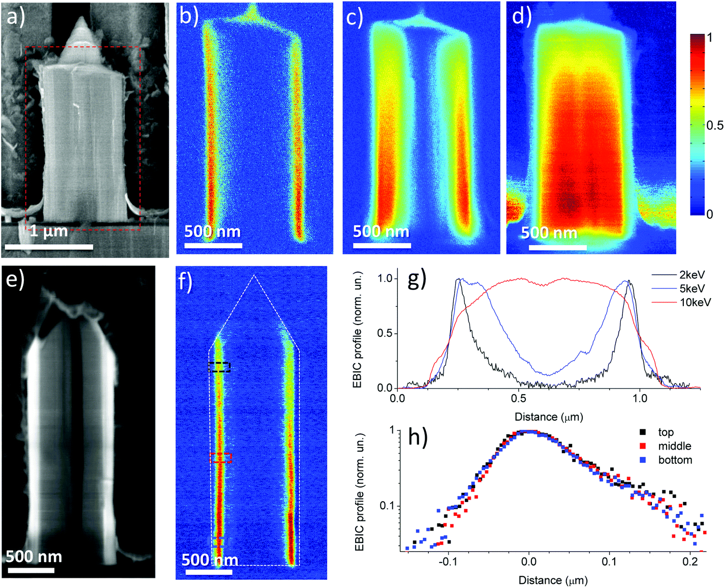 | ||
| Fig. 3 (a) Cross sectional SEM image of the cleaved NW_1 at Vacc = 5 kV. (b)–(d) Normalized EBIC maps corresponding to the red rectangle in panel (a) collected for Vacc and the beam current impinging the sample of (b) −2 kV, 0.4 nA, (c) −5 kV, 0.5 nA and (d) −10 kV, 0.9 nA. (e) Cross sectional SEM image of the cleaved NW_2 at Vacc = 2 kV. (f) Corresponding EBIC map collected for Vacc = 2 kV and beam current 0.4 nA. The dashed line indicates the nanowire perimeter. The normalized color scale is the same for panels (b, c, d and f). (g) EBIC profiles at Vacc = 2 kV, 5 kV and 10 kV at the half height of the NW_1 perpendicular to the wire axis. (h) EBIC profiles at the top, middle and bottom part of the NW_2 perpendicular to the wire axis at locations marked with dashed rectangles in panel (f). | ||
The first nanowire (denoted NW_1) shown in Fig. 3(a) is broken at about one half of its total length allowing to partly observe a top broken surface. NW_1 is cleaved close to its axis since the SiN mask opening is seen in the SEM image of Fig. 3(a). Fig. 3(b)–(d) show the EBIC maps of this wire for acceleration voltages increasing from 2 kV to 10 kV and Fig. 3(g) gives the corresponding EBIC profiles at half-height perpendicular to the wire axis. Depending on the Vacc different material volumes are excited corresponding to different regions of the core–shell p–n junction. At Vacc = 2 kV (beam current 0.4 nA), the EBIC signal appears as two stripes localized at both sides of the wire in correspondence to the p–n junctions perpendicular to the image plane. The back side of the nanowire does not contribute to the signal except on the top broken facet, where a bright contour of the p–n junction on the back facets can be distinguished. When the acceleration voltage is increased to 5 kV (beam current 0.5 nA), the EBIC stripes broaden. The electron penetration depth at 5 kV is estimated to be close to 250 nm for a nitride 2D layer,26 so that the p–n junction on the back facets starts to be excited except for the central part of the wire. Finally, at Vacc = 10 kV (beam current 0.9 nA) the penetration depth (estimated to be 650 nm) exceeds the thickness of the cleaved nanowire so that the EBIC signal appears at all excitation positions.
The second nanowire (denoted NW_2) shown in Fig. 3(e) is cleaved over its entire length. It is interesting to note that for the SEM operated at low acceleration voltage (2 kV for Fig. 3(e)) in slow scan mode the image reveals the nanowire internal structure via a strong doping-related contrast. The p-doped GaN shell appears almost white while the heavily n-doped GaN core exhibits a dark contrast. Doping contrast imaging in low voltage SEM is a well-known technique used for wafer inspection.28,29 The imaging contrast is related to modification of surface properties with doping and in particular to surface band bending.29
The EBIC map acquired at Vacc = 2 kV (beam current 0.4 nA) of NW_2 is shown in Fig. 3(f). The EBIC signal extends over the entire length of the cylindrical nanowire part in correspondence to the radial p–n junction on the m-planes. (The signal perturbation on the right side of the wire reflects the cleavage imperfections.) Some signal is visible in the lower part of semi-polar facets, however it rapidly quenches towards the tip, which confirms the conclusions drawn from the top-view EBIC maps that the major part of the semi-polar facets is electrically inactive.
To probe the homogeneity of the material properties along the wire axis, EBIC profiles perpendicular to the growth axis have been extracted at three positions of the NW_2 in the bottom, middle and top parts of the wire (Fig. 3h). Within the experimental accuracy, no modification of the EBIC profile shape is observed between these positions, which means that the material properties, namely the doping level and the non-radiative recombination losses are homogeneous along the wire axis. The profiles present an exponential behavior with a characteristic length of 70 ± 10 nm in the n-doped GaN underlayer and of 25 ± 5 nm in the p-doped GaN shell. It should be noted that the profiles are given by the convolution of the collection efficiency and the excitation volume (for the used Vacc = 2 kV the penetration depth is calculated to be 50 nm).
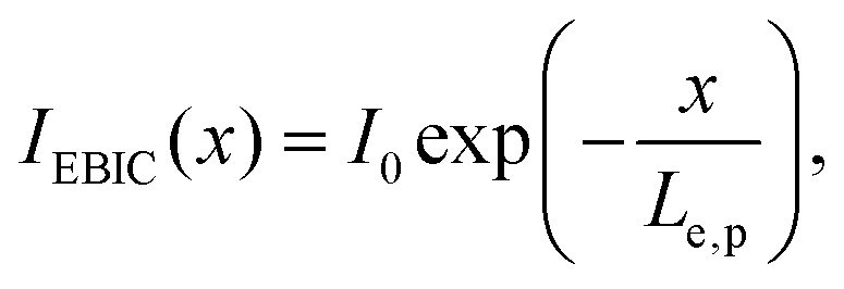
It is well known that the EBIC profiles can be used to extract the minority carrier diffusion length by using different models describing the carrier diffusion.30–34 The simplest approach neglecting surface trapping and recombination consists in an exponential fit of the EBIC profile on both sides of the p–n junction30,31
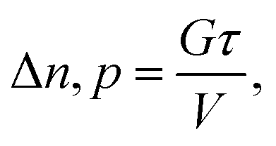
where G is the generation rate of electro/hole pairs, V is the generation volume (calculated to be equal to 5.2 × 10⁻¹⁶ cm−3, 3 × 10⁻¹⁵ cm−3, 1.1 × 10⁻¹⁴ cm−3, 3.9 × 10⁻¹⁴ cm−3 for Vacc of 2 kV, 3 kV, 4 kV and 5 kV, respectively) and τ is the carrier lifetime (taken to be 2 ns (ref. 36)). The generation rate is expressed as20
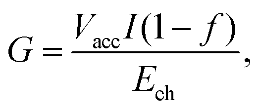
where I is the beam current impinging the sample surface, f is the fraction of the electron beam energy that is reflected (f value lies between 0.125 and 0.135 for the considered Vacc range20) and Eeh is the energy expended by the incident electrons in the formation of an e/h pair (Eeh corresponds to approximately three times the bandgap energy of GaN).20 Note that in this estimation the generated carrier density is approximated as being constant within the excitation volume. The calculated carrier density is 2 × 1018 cm−3 at Vacc = 2 kV, 5 × 1017 cm−3 at 3 kV, 2 × 1017 cm−3 at 4 kV and 7 × 1016 cm−3 at 5 kV. By comparing the generated carrier concentration with the equilibrium carrier concentration due to the doping (in our case ∼5 × 1018 cm−3 for electrons and ∼5 × 1017 cm−3 for holes), the assumption of weak injection conditions starts to be valid above 3 kV for the hole diffusion in the n-GaN underlayer and above 4 kV for the electron diffusion in the p-GaN shell. If the weak injection conditions are not satisfied, both types of carriers play a role and the diffusion is ambipolar. Therefore, although the EBIC profiles of Fig. 3(h) can be well fitted with an exponential dependence, the extracted characteristic lengths cannot be directly related to the minority carrier diffusion length. In addition, at low Vacc surface recombination may have a significant impact lowering the obtained diffusion lengths. While a low acceleration voltage is advantageous to achieve high spatial resolution maps, a high acceleration voltage is desirable to correctly measure the diffusion lengths. However, due to the small nanowire diameter, for Vacc > 4 kV the EBIC signal is a superposition of the cleaved p–n junction signal and the p–n junction signal from the back facets (cf. for example Fig. 3c). This results in a 3D diffusion, which cannot be described by a simple 1D model, making the extraction of the minority carrier diffusion length very complicated. However, it should be noted that the LED operation is governed by the majority carrier injection and recombination, so that the exact values of minority carrier diffusion length are not of critical importance for this kind of devices. On the contrary, for LED operation it is important to probe the homogeneity of the material parameters along the wire axis. The information on the homogeneity can indeed be extracted from cross-sectional EBIC maps because even under strong excitation conditions the EBIC signal decrease away from the junction is related to diffusion and is affected by the material quality via non-radiative carrier losses. Therefore, the constant shape of the EBIC profile at different places of the nanowire is a demonstration of the homogeneity along the wire axis of minority carrier diffusion lengths and doping concentrations in GaN underlayer and shell.
Correlation between the cathodoluminescence and EBIC profiles
We now analyze the variation of the magnitude of the EBIC signal along the wire axis. As shown by the vertical EBIC profile of Fig. 4(b), the EBIC signal decreases in the vertical direction towards the nanowire top. The reduction of the EBIC signal may have different origins. Indeed, the induced current depends on the generation efficiency (determined by the beam/semiconductor interaction), the carrier separation and extraction by the p–n junction (determined by the junction parameters and the carrier recombination rate), the perpendicular transport in the p-type shell and finally the parallel transport in n-doped region along the wire axis toward the contact (determined by the core and underlayer resistivity).20 The generation efficiency is mainly determined by the beam parameters and the interaction volume and can be assumed constant over the cylindrical nanowire part. Due to the high doping level of the n-GaN, the core and underlayer are expected to be equipotential and the transport efficiency is close to unity.20 Therefore the factor responsible for the EBIC signal variation should be the variation of the properties of the p–n junction. The lower EBIC signal at the top could potentially be attributed to a higher defect density in the top nanowire part increasing the non-radiative recombination. However the hypothesis of an increase of the defect density is in contradiction with the constant shape of the horizontal EBIC profile at different positions along the wire axis, as discussed previously.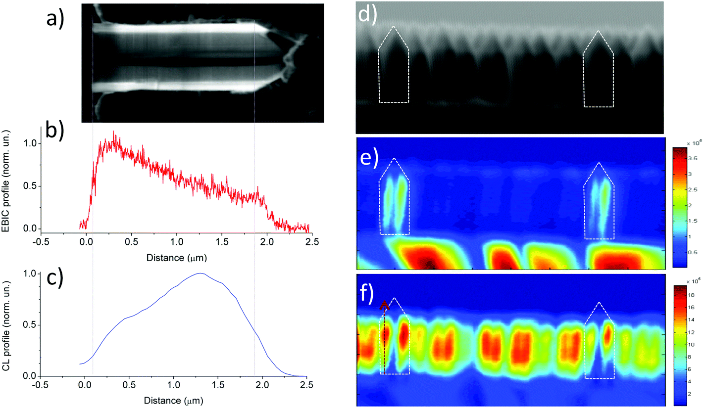 | ||
| Fig. 4 (a) SEM image of a cleaved NW (vertical lines indicate the positions corresponding to the nanowire base and to the end of the m-plane, respectively). (b) Normalized EBIC profile parallel to the wire axis (corresponding to the EBIC map of Fig. 3(f)). (c) Normalized CL profile spectrally filtered for quantum well emission wavelengths from 390 nm to 550 nm parallel to the wire axis. (d) Cross sectional SEM image of the studied region acquired in the CL set-up. (White dashed polygons indicate the cleaved nanowires.) (e) CL map at Vacc = 5 kV spectrally filtered for GaN near band edge emission energies between 3.2 and 3.53 eV. (f) CL map spectrally filtered for quantum well emission wavelengths from 390 nm to 550 nm at Vacc = 5 kV. Note that the CL and the EBIC profiles have been measured on different nanowires. | ||
To better understand the origin of the EBIC signal reduction, CL mapping under Vacc = 5 kV at room temperature has been performed on the sample cross section. The CL experiments have been performed in an SEM microscope JEOL 7001F. The spectral images were recorded with a Jobin Yvon Spectrometer HR320 coupled with a CCD camera. Fig. 4(e) shows a CL map spectrally filtered for the quantum well emission wavelengths (390 nm–550 nm). To easily identify cleaved nanowires, a CL map of the same region spectrally filtered for emission energies between 3.2 and 3.53 eV corresponding to the near band edge emission of GaN is shown in Fig. 4(d). The emission of the p-doped shell is weak because of a high Mg concentration and of non-radiative recombinations on the lateral surface, whereas the emission of the n-GaN underlayer is much stronger. Therefore the cleaved nanowires for which the underlayer is directly exposed to electron excitation appear as bright double stripes in Fig. 4(d). It should be noted that the GaN near band gap emission of the nanowires represents only 10% of the total CL intensity, the main contribution arises from the InGaN quantum well.
Fig. 4(c) shows the CL profile parallel to the wire axis corresponding to the map of the panel (e). It is seen that the emission intensity increases toward the nanowire top. This observation further contradicts the hypothesis of a degradation of the material quality toward the top of the m-planes. We attribute this effect to a gradient of the In composition in the quantum well: the In content progressively increases from ∼0.13 to ∼0.18 along the m-planes from the bottom to the top as evidenced by the above-described EDX structural measurements. This effect is also illustrated in Fig. S3 of the ESI,† which displays the CL spectra for the excitation at the nanowire base and in the upper part. The peak wavelength is redshifted by ∼50 nm for the two excitation positions. With increasing In composition the quantum well depth increases and consequently the carrier extraction becomes less efficient. The carriers are trapped in the quantum well for a longer time and the recombination probability increases. In addition, the carrier extraction efficiency is reduced because of the increase of the Al content in the electron blocking layer from ∼0.09 in the base part to ∼0.19 in the top part of the m-plane as evidenced by the above-described EDX measurements. The reduction of the extraction efficiency explains both the increase of the CL signal and the decrease of the EBIC signal along the wire axis. It is difficult to make quantitative measurements of CL to quantify the percentage of generated carriers producing luminescence, however the opposite trends observed for CL and EBIC indicate that the decrease of the electrical signal may be compensated by the increase of the light emission. We conclude that the reduction of the EBIC toward the nanowire top is not due to degradation of the material quality, but to the compositional variations in the quantum well and in the electron blocking layer leading to a reduction of the extraction efficiency and to an increase of the carrier recombination in the quantum well. It should be noted that because of the need for a freshly cleaved surface for both experiments, the CL and the EBIC profiles have been measured on different nanowires that may have slightly different In compositional gradient. This may explain the difference between the EBIC and CL profile derivatives, which do not exactly compensate each other. However, an abrupt decrease of the CL intensity is observed close to the m-plane/semi-polar plane junction (coordinates larger than 1.5 μm), which may be due to the contribution of non-radiative defects in the upper In-rich part of the quantum well.
Transitory EBIC signal
During the cross sectional EBIC observations an unusual behavior has been observed. For several wires a weak EBIC signal first appeared at the n-GaN core/n-GaN underlayer junction. This phenomenon is accompanied by a strong suppression of the regular EBIC signal coming from the p–n junction. Under irradiation of the wire with electron beam for about 10 min the EBIC map was modified: the core/underlayer signal disappeared and transformed into a conventional signal from the p–n junction. No further modification of the EBIC map has occurred during more than 1 h of observation. The map transformation is illustrated in Fig. 5: panels 5 (a) and (b) show the SEM image and the EBIC map at the beginning of the observation and panels 5 (c) and (d) correspond to the final state of the wire. A change is observed not only in the EBIC map, but also in the SEM secondary electron images. The secondary electron contrast at the initial stage (panel 5 (a)) indicates some charging of the core region, the charge being redistributed after the transformation (panel 5 (c)).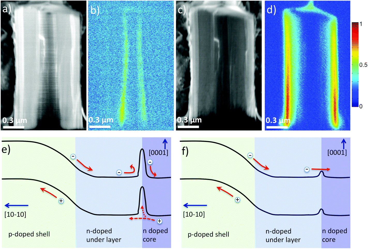 | ||
| Fig. 5 (a) Cross sectional SEM image at Vacc = 3 kV of a cleaved nanowire NW_1 (the dark contrast in the nanowire core is tentatively attributed to charging effects) and (b) corresponding EBIC map before the transformation. (c) and (d) Same after the transformation. EBIC images of panels (b) and (d) are collected under the same conditions and traced in the same color scale. Schematic of the band profile before (e) and after (f) the transition. | ||
It may be supposed that a non-zero signal at the core/underlayer interface may arise from the small doping difference between these two layers. However this assumption cannot explain the absence of EBIC signal at the p–n junction in the initial stage. We suppose that the EBIC signal from the core/underlayer interface can be related to the presence of charged traps at this interface. Separate measurements using electron holography technique37 have evidenced a potential variation at the core/underlayer interface in similar samples. The mechanism that we propose to explain the unexpected EBIC signal is illustrated in Fig. 5(e), which shows the schematized band profile perpendicular to the wire axis. (For simplicity, the electron blocking layer and the quantum well are not represented.) The negatively charged traps at the core/underlayer interface can perturb the band profile and induce separation of generated charges. The proposed mechanism is similar to the case of grain boundaries in ZnO 2D layers.38 At the same time they act as a barrier for electrons generated at the p–n junction preventing their collection by the core. The generated holes can either cross the interface, diffuse toward the p–n junction and be collected or can be trapped at the interface. Hole trapping compensates the negative charge and decreases the potential barrier associated with the interface so that it becomes transparent for electrons as illustrated in Fig. 5(f). This leads to a reduction of the EBIC signal from the core/underlayer interface and the appearance of the normal EBIC signal from the p–n junction. The signal modification is persistent: the same nanowire observed 1 h after the electron irradiation has been stopped, presented the normal EBIC signal from the p–n junction and no signal from the core/underlayer interface. This suggests that the electron beam treatment may lead to trap healing. Note that a suppression of the EBIC contrast due to a modification of a defect charge state under electron beam irradiation has previously been reported in InGaN/GaN 2D structures.39
At this stage we cannot identify the nature of charged traps at the core/underlayer interface, it will be further investigated in a dedicated structural study. However, it is important to note that the observed electrical activity of the core/underlayer interface is undesirable for the LED operation since it may affect the current injection. Indeed, a potential barrier at this interface increases the access resistance. In addition, if the height of this barrier is different from wire to wire, this may lead to a wire-to-wire injection inhomogeneity. Therefore, special attention should be paid to the growth stage at which the switching between the axial and lateral growth modes is performed in order to achieve a perfectly clean and defect-free core/underlayer interface.
Conclusion
We have applied EBIC and CL microscopies to investigate the structural, electrical and optical properties of nanowire radial InGaN/GaN LED structures. The electrical activity of the p–n junction on the m-planes and on the semipolar planes is directly imaged in top view and cross-sectional geometries. The cross-sectional EBIC and CL maps demonstrate the absence of defects and a good homogeneity of the doping and minority carrier diffusion lengths along the wire axis. The EBIC current reduces toward the nanowire top while the luminescence intensity increases, which is explained by the compositional gradients in the InGaN quantum well and in the AlGaN electron blocking layer. Finally, the electrical activity of the core/underlayer interface is evidenced in several nanowires and is attributed to charged traps at this interface creating a type II potential barrier. Saturation of these defects under electron beam irradiation is observed.Acknowledgements
This work has been partially financially supported by Laboratory of Excellency ‘GaNeX’ and ‘NanoSaclay’, by FP7 Marie Curie projects ‘Funprob’ and ‘NanoEmbrace’, by EU project “NWs4LIGHT” (grant no. 280773), and EU ERC project “NanoHarvest” (grant no. 639052). A. Babichev acknowledges the support of RFBR (Project number 14-02-31485, 15-02-08282), and of Scholarship of the President of the Russian Federation (Grant number SP-4716.2015.1). The device processing has been performed at CTU-IEF-Minerve technological platform, member of the Renatech RTB network. The financial support from RTRA for the purchase of the EBIC equipment is acknowledged. For using Dual-beam FEI SCIOS system, the support from the ANR program of future investment TEMPOS-NANOTEM (No. ANR-10-EQPX-50) is acknowledged.Notes and references
- H. J. Leamy, J. Appl. Phys., 1982, 53(6), R51 CrossRef CAS PubMed.
- J. C. Gonzalez, K. L. Bunker and P. E. Russell, Appl. Phys. Lett., 2001, 79(10), 1567 CrossRef CAS PubMed.
- C. L. Progl, C. M. Parish, J. P. Vitarelli and P. E. Russell, Appl. Phys. Lett., 2008, 92(24), 242103 CrossRef PubMed.
- T. Egawa, H. Ishikawa, T. Jimbo and M. Umeno, Appl. Phys. Lett., 1996, 69(6), 830 CrossRef CAS PubMed.
- G. Moldovan, P. Kazemian, P. R. Edwards, V. K. Ong, O. Kurniawan and C. J. Humphreys, Ultramicroscopy, 2007, 107(4), 382 CrossRef CAS PubMed.
- S. Li and A. J. Waag, J. Appl. Phys., 2012, 111(7), 071101 CrossRef PubMed.
- M. S. Kang, C. H. Lee, J. B. Park, H. Yoo and G. C. Yi, Nano Energy, 2012, 1(3), 391 CrossRef CAS PubMed.
- F. Römer, M. Deppner, Z. Andreev, C. Kölper, M. Sabathil, M. Straßburg, J. Ledig, S. Li, A. Waag and B. Witzigmann, Proc. SPIE, 8255, 82550H-1, DOI:10.1117/12.908207.
- M. Tchernycheva, L. Rigutti, G. Jacopin, A. de Luna Bugallo, P. Lavenus, F. H. Julien, M. Timofeeva, A. D. Bouravleuv, G. E. Cirlin, V. Dhaka, H. Lipsanen and L. Largeau, Nanotechnology, 2012, 23(26), 265402 CrossRef CAS PubMed.
- F. Limbach, C. Hauswald, J. Lähnemann, M. Wölz, O. Brandt, A. Trampert, M. Hanke, U. Jahn, R. Calarco, L. Geelhaar and H. Riechert, Nanotechnology, 2012, 23, 465301 CrossRef CAS PubMed.
- L. Yu, L. Rigutti, M. Tchernycheva, S. Misra, M. Foldyna, G. Picardi and P. R. i. Cabarrocas, Nanotechnology, 2013, 24(27), 275401 CrossRef PubMed.
- K. Arstila, T. Hantschel, A. Schulze, A. Vandooren, A. S. Verhulst, R. Rooyackers and W. Vandervorst, Microelectron. Eng., 2013, 105, 99 CrossRef CAS PubMed.
- A. Ng, J. D. Poplawsky, C. Li, S. J. Pennycook and S. J. Rosenthal, J. Phys. Chem. Lett., 2014, 5(5), 856 CrossRef CAS.
- P. Tchoulfian, F. Donatini, F. Levy, A. Dussaigne, P. Ferret and J. Pernot, Nano Lett., 2014, 14(6), 3491 CrossRef CAS PubMed.
- S. W. Schmitt, G. Brönstrup, G. Shalev, S. K. Srivastava, M. Y. Bashouti, G. H. Döhler and S. H. Christiansen, Nanoscale, 2014, 6, 7897 RSC.
- A. Gustafsson, M. T. Björk and L. Samuelson, Nanotechnology, 2007, 18(20), 205306 CrossRef.
- C. Gutsche, R. Niepelt, M. Gnauck, A. Lysov, W. Prost, C. Ronning and F. J. Tegude, Nano Lett., 2012, 12(3), 1453 CrossRef CAS PubMed.
- C. C. Chang, C. Y. Chi, M. Yao, N. Huang, C. C. Chen, J. Theiss, A. W. Bushmaker, S. Lalumondiere, T.-W. Yeh, M. L. Povinelli, C. Zhou, P. D. Dapkus and S. B. Cronin, Nano Lett., 2012, 12(9), 4484 CrossRef CAS PubMed.
- C. Y. Chen, A. Shik, A. Pitanti, A. Tredicucci, D. Ercolani, L. Sorba, F. Beltram and H. E. Ruda, Appl. Phys. Lett., 2012, 101(6), 063116 CrossRef PubMed.
- P. Lavenus, A. Messanvi, L. Rigutti, A. D. L. Bugallo, H. Zhang, F. Bayle, F. H. Julien, J. Eymery, C. Durand and M. Tchernycheva, Nanotechnology, 2014, 25(25), 255201 CrossRef CAS PubMed.
- M. Tchernycheva, P. Lavenus, H. Zhang, A. V. Babichev, G. Jacopin, M. Shahmohammadi, F. H. Julien, R. Ciechonski, G. Vescovi and O. Kryliouk, Nano Lett., 2014, 14, 2456 CrossRef CAS PubMed.
- D. E. Perea, E. R. Hemesath, E. J. Schwalbach, J. L. Lensch-Falk, P. W. Voorhees and L. J. Lauhon, Nat. Nanotechnol., 2009, 4, 315 CrossRef CAS PubMed.
- S. Zhao, S. Fathololoumi, K. H. Bevan, D. P. Liu, M. G. Kibria, Q. Li, G. T. Wang, H. Guo and Z. Mi, Nano Lett., 2012, 12, 2877 CrossRef CAS PubMed.
- J. R. Riley, S. Padalkar, Q. Li, P. Lu, D. D. Koleske, J. J. Wierer and L. J. Lauhon, Nano Lett., 2013, 13(9), 4317 CrossRef CAS PubMed.
- K.-S. Kim, J.-H. Kim and S. N. Cho, IEEE Photonics Technol. Lett., 2011, 23(8), 483 CrossRef CAS.
- Monte CArlo SImulation of electroN trajectory in sOlids, http://www.gel.usherbrooke.ca/casino/, accessed: December, 2014.
- Y. J. Hong, C.-H. Lee, A. Yoon, M. Kim, H.-K. Seong, H. J. Chung, C. Sone, Y. J. Park and G.-C. Yi, Adv. Mater., 2011, 23, 3284 CrossRef CAS PubMed.
- D. Venables, H. Jain and D. C. Collins, J. Vac. Sci. Technol., B, 1998, 16(1), 362 CAS.
- M. El-Gomati, F. Zaggout, H. Jayacody, S. Tear and K. Wilson, Surf. Interface Anal., 2005, 37(11), 901 CrossRef CAS PubMed.
- W. Van Roosbroeck, J. Appl. Phys., 1955, 26(4), 380 CrossRef PubMed.
- J. F. Bresse, J. Microsc. Spectrosc. Electron., 1981, 6(1), 17 CAS.
- F. Berz and H. K. Kuiken, Solid-State Electron., 1976, 19, 437 CrossRef.
- C. Donolato, Solid-State Electron., 1982, 25, 1077 CrossRef CAS.
- S. Guermazi, A. Toureille, C. Grill and B. El Jani, Eur. Phys. J.: Appl. Phys., 2000, 9(01), 43 CrossRef CAS.
- K. L. Bunker, Development and Application of Electron Beam Induced Current and Cathodoluminescence Analytical Techniques for Characterization of Gallium Nitride-Based Devices, North Carolina State University, Raleigh, North Carolina, February, 2005 Search PubMed.
- J. Mickevičius, M. S. Shur, R. S. Qhalid Fareed, J. P. Zhang, R. Gaska and G. Tamulaitis, Appl. Phys. Lett., 2005, 87, 241918 CrossRef PubMed.
- S. Yazdi, T. Kasama, M. Beleggia, R. Ciechonski, O. Kryliouk and J. B. Wagner, Microsc. Microanal., 2013, 19(Supplement S2), 1502, DOI:10.1017/S1431927613009501.
- C. Leach, J. Eur. Ceram. Soc., 2001, 21, 2127 CrossRef CAS.
- P. S. Vergeles and E. B. Yakimov, J. Phys., 2011, 281(1), 012013 Search PubMed.
Footnote |
| † Electronic supplementary information (ESI) available: Additional experimental details, data on the simulation of the EBIC maps and CL spectra. See DOI: 10.1039/c5nr00623f |
| This journal is © The Royal Society of Chemistry 2015 |