
 Open Access Article
 This Open Access Article is licensed under a Creative Commons Attribution-Non Commercial 3.0 Unported Licence
Color generation via subwavelength plasmonic nanostructures
Yinghong
Gu
a,
Lei
Zhang
a,
Joel K. W.
Yang
bc,
Swee Ping
Yeo
a and
Cheng-Wei
Qiu
*a
aDepartment of Electrical and Computer Engineering, National University of Singapore, Singapore 117583, Singapore. E-mail: chengwei.qiu@nus.edu.sg
bInstitute of Materials Research and Engineering, Agency for Science, Technology and Research, 3 Research Link, Singapore 117602, Singapore
cSingapore University of Technology and Design, Engineering Product Development, Singapore 138682, Singapore
First published on 16th March 2015
Abstract
Recent developments in color filtering and display technologies have focused predominantly on high resolution, color vibrancy, high efficiency, and slim dimensions. To achieve these goals, metallic nanostructures have attracted extensive research interest due to their abilities to manipulate the properties of light through surface plasmon resonances. In this paper, we review recent representative developments in plasmonic color engineering at the nanoscale using subwavelength nanostructures, demonstrating their great potential in high-resolution and high-fidelity color rendering, spectral filtering applications, holography, three-dimensional stereoscopic imaging, etc.
1. Introduction
In nature, colors are mainly produced by the light scattering or partial absorption of materials. Color displays such as emissive liquid-crystal displays employ pigment-based color filters to absorb the complementary colors to produce the red, green, and blue channels.1–3 With the drive towards higher-resolution imaging and displays, new innovations are needed to achieve higher resolution, lower power consumption, higher compactness, and also color tunability in devices. The highest possible resolution in theory for color display and imaging is set by the diffraction limit of the accompanying optics,4 which is ∼250 nm pitch for imaging through high numerical-aperture objectives with visible light. However, the resolution of the existing pigment-based color printing can just reach the level of ten micrometers, still 1 or 2 orders away from this target.Alternatively, colors can also be generated by structure engineering, such as diffraction optic devices, photonic crystals, and plasmonic structures. Some naturally occurring photonic structures generate the colorful appearance of some types of insects, birds and aquatic animals,5–12 usually with the combined effects of thin film/multilayer interferences, grating diffraction, photonic crystals and light scattering. An example of natural structural color is butterfly wings, which has been widely investigated and reproduced through nanostructures fabricated in labs.7–12 It has been demonstrated that this structural color effect based on photonic crystals, nanowire arrays and polycarbonate (PC) or other dielectric multilayered nanostructures can be useful in optical applications,13–18 such as color generation by the patterned arrays of silicon nanowires13–15 and nanowire-based wavelength selective photodetectors.16
However, the size of unit cells of these non-plasmonic nanostructures is in the order of the wavelength of light, usually in micrometer dimensions. This means that there is still room for further improvements to reach the diffraction limit. To go beyond the natural color generation, surface plasmon resonances (SPRs) open a promising way to control colors with high efficiency and high resolution due to the development of nano-fabrication technologies. The interaction between light and plasmonic nanostructures has been shown to manipulate the intensity, phase, and polarization of scattering light.19–27 Thus plasmonic nanostructures are promising for use in high-resolution color displays and imaging applications due to their small dimensions and the ability to manipulate light efficiently.28–30 The sub-wavelength plasmonic elements enable the structure to be ultra-thin, usually 1–2 orders of magnitude thinner than pigment-based filters, making it favourable for integration and miniaturization of display devices. Plasmonic color filters with a periodic sub-wavelength hole array in a metal film can achieve high transmission efficiencies due to the phenomenon of extraordinary optical transmission (EOT),19,20,22,31 which is an important consideration in reducing power consumption. Moreover, the energy absorbed by a multi-layered nano-grating filter can be harvested and converted to electrical energy while producing desirable colors in the visible band,32 making it energy-efficient and suitable for electro-optic applications. Recently, color printing with plasmonic nanostructures has demonstrated the resolution of 100![[thin space (1/6-em)]](https://www.rsc.org/images/entities/char_2009.gif) 000 dots per inch (d. p. i.), which is already at the diffraction limit.33 This high-resolution plasmonic color printing technology has significance in optical data storage, digital imaging, and in security applications. In addition, although some plasmonic nanostructures are designed to avoid incident angle dependence,34 it is also useful for developing active color filters with controllable output based on sensitivities to the incident angle or polarization.35,36 With these advantages, the plasmonic nanostructures have great potential in color filtering and imaging applications such as digital photography and digital displays.
000 dots per inch (d. p. i.), which is already at the diffraction limit.33 This high-resolution plasmonic color printing technology has significance in optical data storage, digital imaging, and in security applications. In addition, although some plasmonic nanostructures are designed to avoid incident angle dependence,34 it is also useful for developing active color filters with controllable output based on sensitivities to the incident angle or polarization.35,36 With these advantages, the plasmonic nanostructures have great potential in color filtering and imaging applications such as digital photography and digital displays.
This paper provides an overview of the most recent development of nanostructural color filtering and imaging nanotechnologies, and several kinds of representative nanostructures that perform well in color filtering and imaging or that have special functionalities are presented. We discuss the advantages and potential for practical applications as well as their limitations.
2. Color generation of plasmonic nanostructures
Surface plasmons (SPs) are collective free-electron oscillations at the metal-dielectric interfaces. They exhibit enhanced near-field amplitude of the electric field at the resonance wavelength. This field is highly localized and decays exponentially away from the metal–dielectric interface.37–41 Unlike the photon absorption in pigments, which is determined by the energy level transitions of the molecules, the scattering and absorption of plasmonic nanostructures are determined by their geometry and dimensions. Leveraging on the development of nanofabrication technologies such as electron-beam lithography (EBL) and focused ion beam (FIB), the shape and size of metallic nanostructures can be well-controlled with sub-10 nm precision.42,43 With these sub-wavelength elements, the pixels of color imaging can be extremely small and the resolution can be improved up to the diffraction limit, with a thickness of the resonators of only tens of nanometers. In addition to the advantage of high resolution and ultrathin characteristics, plasmonic nanostructures have also the following attributes: (1) as the nanostructures are made of metal, they are chemically stable and can endure long-duration ultraviolet irradiation and high temperatures compared to chemical pigments; (2) the device can realize a broad range of colors using a single element of metals, by just varying the lateral size and geometry of the structures. This avoids the sequential deposition of inks and reduces the process steps and misalignment between the color channels; (3) the SPRs can be tuned by factors such as the environment index, the incident angle and polarization, and it is possible to make the optical element active,35,36,44–48 which could be useful for a dense optical data archival,49 and contributes to security applications.2.1 Structural color from the localized surface plasmon resonance (LSPR)
 | (1) |
 | (2) |
 | (3) |
 | ||
| Fig. 1 (a) Scanning electron microscope (SEM) image of the top view of Ag vertical nanorod arrays on a quartz substrate with a periodicity p = 550 nm. (b) Optical image of the reflective colors from different Ag nanorod arrays. (c) Measured reflection spectra of the corresponding arrays as a function of wavelengths. The table below (c) shows the size parameters of nanostructures for different colors in (b) and (c). Reproduced with permission.50 Copyright 2013, RSC. | ||
The dimension of the nanorods in Fig. 1a is optimized to enhance efficiency, and the reflected color is controlled by the diameter and periodicity of the nanorod array. To achieve the full color band, especially the blue color, a small periodicity and high diameter/periodicity (d/p, up to 0.938) ratio of the nanostructure is required, which means the gap between two nanorods needs to be ultra small (about 20 nm), as shown in the table in Fig. 1c. This requires high fabrication accuracy, but on the other hand, provides high resolution. The periodicity is close to the wavelength, so it is possible to form pixels that are much smaller than those of conventional chemical pigment-based methods.
Due to the circular symmetry of the structures, the nanorod array responds equally to different polarized incident lights. However, the polarization dependence of the plasmonic nanostructures can also be utilized in color filtering and imaging applications. Polarization dependence of plasmonic nanostructures has been well studied in the past few years. For instance, nanostructures composed of metallic crosses with different arm lengths35 exhibit strong dependence on the polarization states. As shown in Fig. 2a, b, only either vertical or horizontal polarized incident light can excite the LSPR of their corresponding arms, so that they have different transmission spectra and render different colors. At the arbitrary polarization angle φ, the transmission spectra is a linear superposition of the vertical and horizontal states, represented as
| T(φ, λ) = TV(λ)sin2φ + TH(λ)cos2φ | (4) |
 | ||
| Fig. 2 (a–c) Conversion of the polarization state to a visible color by cross nanoantennas: (a) polarized white light is color filtered by the LSPs on the arms of the cross nanoantennas; the output color results from the additive color mixing of the filtering functions of the two arms of the cross. (b) Simulated transmission spectra for linearly polarized illumination with the polarization angles ranging from φ = 0°, at which yellow is blocked, to φ = 90°, at which blue is blocked, in steps of 10°. (c(i)–(xi)) c(i) Schematic representation of the experimental setup. c(ii)–(v) Transmission images of the LSP pattern sample for (ii) unpolarized incident light, (iii) 90°, (iv) 45° and (v) 0° polarized light. c(vi)–(xi) Transmission images of the twisted sample for 0°–90° polarized light in steps of 30°. (d) SEM image of a part of the LSP sample. (d) Schematic diagram of polarization dependent nanostructures with elliptical nano-pillars and coupled nano-square pair pillars with Al on top and at the bottom. (e) Schematic diagram of polarization dependent nanostructures with Al elliptical nano-disks and coupled nano-square pair pillars with corresponding holes at the bottom Al layers. (f) Optical image of the same area formed from elliptical pixels with different linear polarized incident light. (a–d) Reproduced with permission.35 Copyright 2012, ACS. (e, f) Reproduced with permission.36 Copyright 2014, NPG. | ||
Similar to the cross structures, pixels consisting aluminum (Al) elliptical nano-disks or a coupled nano-square pair with complementary holes at the bottom Al layer,36 as shown in Fig. 2e, can also create different images with different polarized incident light (Fig. 2f). The nanostructure can provide abundant color in a full visible range. The application of these polarization dependent disks–holes nanostructures is further discussed in section 2.3.1.
 | ||
| Fig. 3 (a) Schematic diagram of the grating color filter of 30 nm thick Ag grating with different periods. (b) Measured TM transmission spectra of yellow, magenta and cyan for the structure in (a). (c) Schematic of the grating color filter structure with a buffer layer. (d) Simulated transmission spectra of RGB for the structure in (c). (e) Schematic diagram of the MIM grating color filter. (f) SEM image and optical microscopy image of the pattern “M” formed by the structure in (e) illuminated by white light. (a, b) Reproduced with permission.67 Copyright 2013, NPG. (c, d) Reproduced with permission.69 Copyright 2011, AIP Publishing LLC. (e, f) Reproduced with permission.71 Copyright 2010, NPG. | ||
On the other hand, high efficient additive color filters are greatly valuable as well. An Al grating68 with a high-index dielectric waveguide layer can provide an efficiency of over 70% at transmission peak. The color filtering is achieved by means of the guided mode resonance (GMR) effect.77,78 The GMR between the diffracted modes of grating and the guided modes of the planar dielectric waveguide (with Al grating as the upper cladding and a quartz substrate as the lower cladding) is readily induced as long as phase matching is achieved between them. The transmission is substantially increased when the incident wave constructively interferes with this coupled mode. Furthermore, as shown in Fig. 3c, a similar nanostructure but with a low-index buffer layer between the metal grating and high-index waveguide layer was reported with an improved transmittance of nearly 90%.69 The thickness of the buffer layer can control the loss of the guided mode in metallic gratings, which can be explained by the theory of metal cladding dielectric waveguide.79 Therefore, this nanostructure with a buffer layer can achieve narrow band resonances and high efficiency in the transmission spectra. This characteristic of high and sharp peaks is suitable for producing colors with high purity.
The resonance within the metal–insulator–metal (MIM) structures32,45,70,71,80–84 can be used to filter white light into individual colors as well. The most important limitation of the MIM color filters is their low transmittance, so it is valuable to introduce diffractive effects into MIM structures to improve their efficiency. In Fig. 3e, a MIM grating is constructed by Al–ZnSe–Al resonators. The bottom Al grating is used to couple the incident light into the plasmon waveguide modes by diffraction, and the top Al grating reconverts the confined plasmon into propagating waves by scattering the light to far field in the forward direction, while the ZnSe layer ensures the efficient coupling of SP modes at the top and bottom Al layers. This photon–plasmon–photon conversion efficiently enhances the transmission at a specific wavelength. The periodicity of this MIM grating varies from 200 nm to 400 nm to achieve arbitrary colors; such a small periodicity also helps attaining high resolution for color image and display (in Fig. 3f).
Overall, the most significant advantage of plasmonic grating color filters and images among the plasmonic nanostructures is their high efficiency (usually 60% to 90%). For those grating nanostructures coupled with guided modes, the bandwidth of resonance can be very narrow (with FWHM of 30 nm69), so that the filtered color can be pure. The spatial resolution of these nanostructures is also ultrahigh, close to the diffraction limit.67,71 The period of grating can be minimised to half wavelength, and the length of grating can also be subwavelength, evolving to nanosquare arrays or so-called 2D gratings. Another characteristic of 1D grating is the polarization dependence. Only transverse magnetic (TM) waves (the electric field is perpendicular to the grating direction) can be filtered, while the transverse electric (TE) waves (the electric field is parallel to the grating direction) are mostly reflected or transmitted. Therefore they can actively work for many polarization-related applications as discussed in section 2.1.2.
2.2 Structural color from propagating surface plasmon
As discussed in section 2.1, the LSPR in metallic nanoantennas produces peaks in the reflection spectrum and dips in the transmission spectrum. According to the Babinet's principle,85 the complements of these nanoantennas, which are the hole arrays in metal films, would result in dips in the reflection spectra and peaks in the transmission spectra. While nanoantenna arrays can work as subtractive color filters in the transmission mode, the nanohole arrays on metallic films can work as additive filters, which are needed in many imaging and display applications.Considering a single hole in a metallic film, the transmission efficiency should be proportional to (r/λ)4, where λ is the incident wavelength and r is the radius of the hole.86,87 It means that the transmission of a subwavelength hole would be extremely low. However, the periodic metallic structures can provide the momentum for converting the incident light into SPs, so that the hole arrays on the metal film can give rise to the EOT effect.19,20,22 In the past few years, the hole arrays had been theoretically and experimentally88–107 studied in many aspects, such as the selective extraordinary transmission for color filtering. The wavelength of transmission peak λmax depends on the periodicity and the constituents of the hole arrays. At normal incidence, for the square array
 | (5) |
 | (6) |
where a is the periodicity of the array, εm and εd are the relative permittivities of the metal and dielectric material, and i and j are the scattering orders of the array.86,108,109 Considering the interference of the scattering losses of the holes and the Fano-type interaction,62,110λmax would be slightly blue shifted. Based on the interaction of these modes, the hole arrays can be designed for transmitted color filters.
In particular, for the lowest order mode (i = ±1, j = 0), the SPR peak wavelength of the hexagonal array is smaller than that of the square array with the same period and material. Moreover, the wavelength interval of the transmission peak between the first two modes of a hexagonal array is also larger, which makes the hexagonal array more favorable for reducing the color cross-talk and improving the purity of the color. To a lesser extent, the shape of holes also affects the color, as shown in Fig. 4a, b. The triangular hole arrays give narrower resonance peaks than the circular hole arrays, but with lower efficiency. After comparing them, it is also found that lattice construction has a larger influence on the hole shapes. Interestingly, the hexagonal array performs much better in building a full color map.
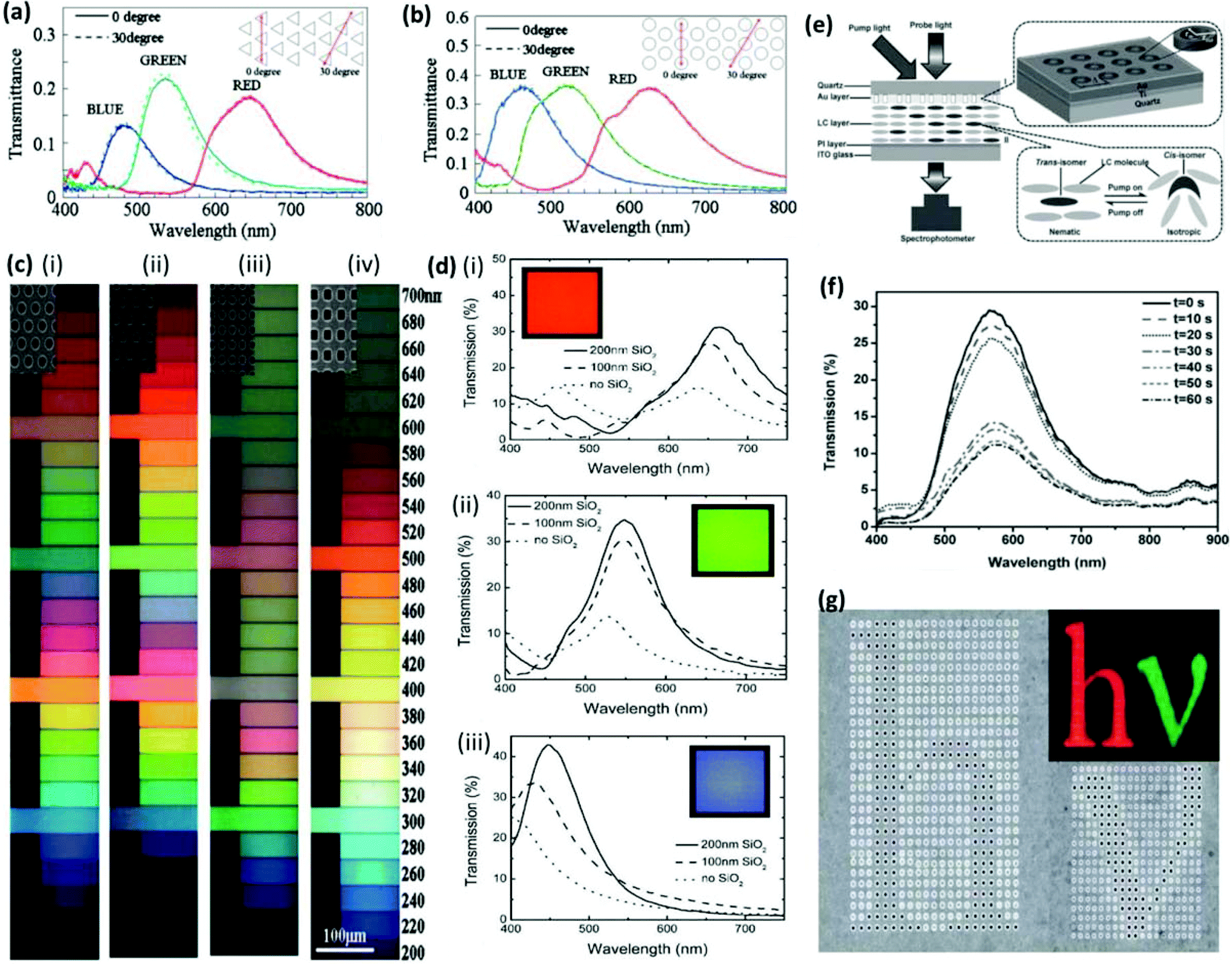 | ||
| Fig. 4 (a–b) Polarization dependence of the transmission spectra of RGB color filters with (a) triangular holes and (b) circular holes in hexagonal array. (c(i)–(iv)) Optical microscope images of Al color filters with (i) circular holes in the hexagonal array, (ii) triangular holes, (iii) circular holes in the square array, and (iv) square holes. (d(i)–(iii)) Measured transmission spectra of RGB color filters of circular hole arrays, with no cap layer, 100 nm and 200 nm SiO2 cap layers. (e) Schematic of the sample structure and experimental setup for color filters with LC layers. The zoom-in part I shows the fabricated square pattern of Au AAAs, and the zoom-in part II shows the working mechanism of the optical driving process in LCs. (f) The evolution of the transmission spectra as a function of time using the UV pump for the color filter with an aperture size of 120 nm. (g) Holes in a dimple array generating the letters “hv” in transmission, with the periods of 550 nm (red color) and 450 nm (green color). (a–c) Reproduced with permission.111 Copyright 2011, AIP Publishing LLC. (d) Reproduced with permission.108 Copyright 2010, OSA. (e, f) Reproduced with permission.47 Copyright 2012, John Wiley and Sons. (g) Reproduced with permission.86 Copyright 2007, NPG. | ||
In experiments, the metallic film with a hole array is usually fabricated on a glass substrate, which leads to an asymmetric dielectric environment. Therefore, the two SP modes on both sides are resonant at different wavelengths, which would reduce the color purity due to the peaks overlapping. Owing to such asymmetry, a momentum mismatch also results in an inefficient coupling between the two sides and then a moderate transmittance. In order to deal with this, an index-matching layer is used to coat the air side.108 As an example shown in Fig. 4d, the transmittance was efficiently improved in the presence of an SiO2 layer in comparison with the case of the absence of SiO2.
As indicated by eqn (1) and (2), the transmission peak could be readily modulated by varying the refractive index of the environment. Recently, an active plasmonic color filter was introduced by overlaying photoresponsive liquid crystals (LCs) onto gold (Au) annular aperture arrays (AAAs),47 as shown in Fig. 4e. The photochromic LC molecules would change their form upon UV irradiation, and further generate a photoinduced refractive index modulation. The transmittance could be greatly reduced as shown in Fig. 4f. Through further improving the tunability of plasmonic color filters with active optical control, an active display might be possible if the RGB compositions could be separately controlled.
The resolution of the metallic hole arrays is much higher than that of chemical pigments, but cannot reach the diffraction limit yet. For example, a color filter with different structures111 is shown in Fig. 4c, while an image of “hν” is displayed with square hole arrays86 in Fig. 4g. The periodicities are all larger than half of the corresponding wavelength, and are sometimes almost comparable to the wavelength.
Overall, the resolution of these nanohole arrays can already satisfy the requirements of most practical applications, with just a last step to the theory limitation. And they can also provide a variety of colors with promising visual effects, as shown in Fig. 4c. However, the transmission efficiency of nanohole arrays is relatively low compared to those color filters utilizing grating nanostructures.
2.3 Structural color from the plasmonic mode coupling
As shown in Fig. 5a, b, a color map is achieved by nanostructures with different gap sizes (g) and disk sizes (D), providing also some really dark colors. It should be noted that the periodicity (D + g) varies from only 80 to 260 nm. In Fig. 5c, an image of Lena is produced by nanostructures with the same periodicity (125 nm) and different disk sizes. Such a small size of nanostructure ensures a resolution at the optical diffraction limit. To enrich the color gamut and increase the practicality of this nano-printing technology, the constituent materials Au and Ag are replaced by Al, which is a preferable metal for plasmonic color printing because of its neutral tint, durability, high reflectance in the visible regime, and low cost. With varied gaps and disk sizes, individual pixels are constructed by mixing disks of different sizes.112 To complement the limited color palette produced by just modifying the gap and disk sizes, dual-size-disk pixels (2 × 2 disks array mixed with different sizes) are constructed, which greatly increased the range of colors and provided an approach for plasmonic color mixing (Fig. 5d, e). The comparison of a “basic” color palette by varying just the Au–Ag disk sizes and the “color-mixing” palette is shown in the micrographs in Fig. 5f, g. Color mixing provides an accurate reproduction of Monet's Impression, Sunrise painting that was poorly reproduced by the primary plasmonic color palette. Further research based on the disk-and-back-reflector-coupled nanostructures realizes 3D plasmonic stereoscopic prints utilizing their polarization dependence.36 Using biaxial color pixels composed of elliptical nanodisk–hole structures (shown in Fig. 2e) can independently control the reflected spectra of orthogonal polarized incident light, so that two different color images can be encoded into the same area. Therefore, the stereoscopic effects can be achieved by fine modulation of the differences between the two images with different polarization.
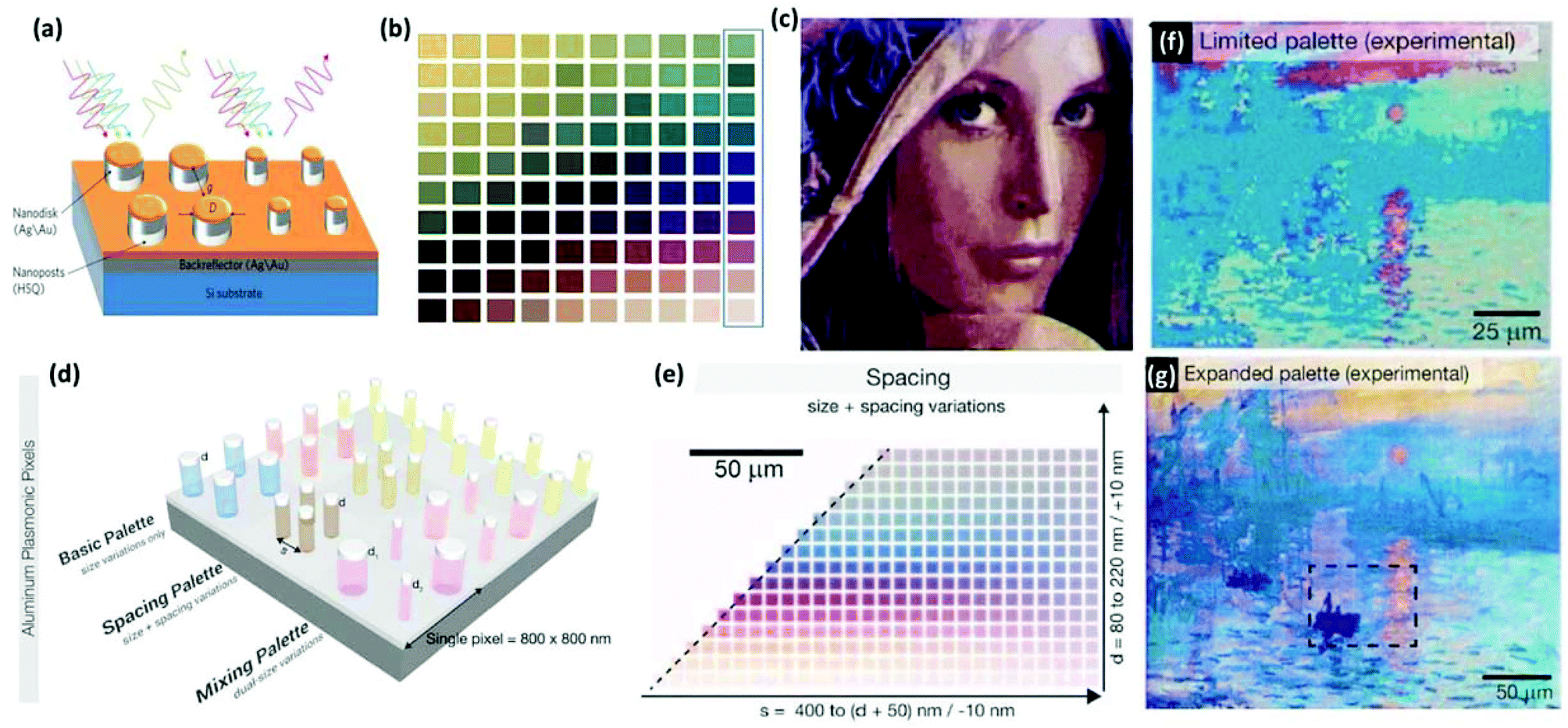 | ||
| Fig. 5 (a) Plasmonic color pixels composed of isolated Au/Ag nanodisks structures set against a back reflector. (b) Full color palettes with the disk size D = 50–140 nm, gap size g = 30–120 nm produced by pixels in (a). (c) Optical micrographs of the Lena image produced by pixels in (a). (d) Plasmonic color pixels composed of Al nanodisks with back reflectors of varying disk size palettes, varying disk sizes and spacing palettes and mix-disks palettes. (e) Full color palettes for pixels in (d). (f–g) Reproduction of Monet's Impression, Sunrise using (f) basic colors and (g) the expanded colors in (e). (a)–(c) Reproduced with permission.33 Copyright 2012, NPG. (d–g) Reproduced with permission.112 Copyright 2014, ACS. | ||
 | ||
| Fig. 6 (a) Schematic views of a unit cell of a MIM structure with Au (yellow) nanodisks on the SiO2 (blue) layer and the Au layer. (b(i)–(ii)) SEM images of nanodisks with average sizes of (i) 80, (ii)120, and (iii) 270 nm. (c) Optical microscopy images with pixels in (a) comparing an uncovered color print (left) and the same print (right) after covering the sample with 100 nm of PMMA. (d) Schematic of the light funnelling nanostructure and the corresponding SEM image. (e(i)–(iv)) The (i) SEM images and (ii) optical images under white light illumination of fabricated Olympic rings. (iii) TM and (iv) TE polarized light illuminating image of one of the Olympic rings. (f) Schematic of dual-function devices for both color filtering and electrical power generation. (a–c) Reproduced with permission.115 Copyright 2014, ACS. (d), (e) Reproduced with permission.34 Copyright 2013, NPG. (f) Reproduced with permission.32 Copyright 2011, ACS. | ||
Another incident angle independent case is based on Fabry–Perot (FP) cavity modes.34 The structure is shown in Fig. 6d, and the dimensions and periodicity of the structure have been designed to avoid the plasmonic modes excitation relying on grating coupling, which is highly dependent on the incident angles. Instead, the nanostructures concentrate light into the silica nano-grooves based on light funnelling of FP cavity modes. At the designed wavelength, the absorbance can reach over 90% within a ±90 degree angle range for specific structure dimensions, so that it performs well as an angle-independent subtractive reflective color filter. The periodicity of this plasmonic nanostructure is also beyond the diffraction limit of light, and thus it can produce polarization-dependent high resolution images, as shown in Fig. 6e.
In addition, the plasmonic color filter can also be integrated with organic solar cells.32 As shown in Fig. 6f, the MIM nanostructure contains Au nano-grating on the top and an Al film at the bottom, which serve not only as a plasmonic color filter, but also as electrodes for the organic photovoltaic (OPV) cells. By manipulating the periodicity of grating and the thickness of the photoactive layer, the incident light at a specific wavelength can be directly absorbed and then transferred into photocurrents by the OPV structure instead of being wasted as heat, which indicates the great potential of plasmonic nanostructures in electrooptic applications.
3. Summary and outlook
We have reviewed the recent development of plasmonic colors generated by nanostructures. Compared to the conventional pigments and the non-plasmonic structural colors, plasmonic color offers more advantages including ultrasmall dimensions, impressive optical response, wide color tunability and compatibility for device integration. The nano-scaled size of plasmonic structures enables image printing at high resolutions, even beyond the optical diffraction limit. Most structures simply contain one or several ultrathin layers of metallic/dielectric materials, so that their thickness is only tens or hundreds of nanometers. This thin geometry makes it easy to integrate them with miniaturized devices. The well-controlled plasmonic resonance also provides a wide color range and accurately distinguished colors. Moreover, the diversity of plasmonic nanostructures contributes in achieving specific targets, such as high efficiency in transmission or reflection, narrower band-width for purer colors, reduced incident angle dependence, tunable polarization applications, and electro-optic modulations.Although plasmonic nanostructures have so many advantages and great potential in next generation color relevant applications, the first commercial applications would require a drastic reduction in patterning costs. Fabrication methods such as EBL and FIB are necessary to create master templates from which high-throughput replication processes such as nanoimprint can be used to create a large volume of copies. The commonly used plasmonic materials, Au and Ag, are also expensive for mass production, leading to the recent trend towards using Al, which is also CMOS compatible. In addition to cost reduction, the performance of plasmonic devices needs to be comparable to, or better than, existing technologies. For instance, in the application of plasmonic color filters for digital imaging products, the limiting factor is still the insufficient transmittance when compared to pigment-based filters. Hence, while many novel phenomena have been reported in the literature, a strong need now is to significantly improve the optical performance of plasmonic color structures.
In summary, plasmonic nanostructures show great potential in the development of color filtering, high-resolution display and imaging, optical data storage and security. With improved low-cost fabrication technology, they are slated to offer improved performance and lower cost in applications ranging from digital displays, imaging sensors, molecular sensing to optical security devices and optical data archival.
Acknowledgements
The authors acknowledge the support from the National University of Singapore (grant R-263-000-A45-112).References
- Y. Huo, C. C. Fesenmaier and P. B. Catrysse, Opt. Express, 2010, 18, 5861 CrossRef CAS PubMed.
- H. Koo, M. Chen and P. Pan, Thin Solid Films, 2006, 515, 896 CrossRef CAS PubMed.
- M. C. Gather, A. Köhnen, A. Falcou, H. Becker and K. Meerholz, Adv. Funct. Mater., 2007, 17, 191 CrossRef CAS.
- E. Abbe, Proc. Bristol Nat. Soc., 1874, 1, 200 Search PubMed.
- P. Vukusic and J. R. Sambles, Nature, 2003, 424, 852 CrossRef CAS PubMed.
- M. Sinivasarao, Chem. Rev., 1999, 99, 1935 CrossRef PubMed.
- J. Huang, X. Wang and Z. L. Wang, Nano Lett., 2006, 6, 2325 CrossRef CAS PubMed.
- T. S. Kustandi, H. Y. Low, J. H. Teng, I. Rodriguez and R. Yin, Small, 2009, 5, 574 CrossRef CAS PubMed.
- P. Vukusic, J. R. Sambles, C. R. Lawrence and R. J. Wootton, Proc. R. Soc. London, Ser. B, 1999, 266, 1402 CrossRef.
- S. Kinoshita, S. Yoshioka and K. Kawagoe, Proc. R. Soc. London, Ser. B, 2002, 269, 1417 CrossRef PubMed.
- H. Ghiradella, Appl. Opt., 1991, 30, 3492 CrossRef CAS PubMed.
- C. R. Lawrence, P. Vukusic and J. R. Sambles, Appl. Opt., 2002, 41, 437 CrossRef.
- L. Cao, P. Fan, E. S. Barnard, A. M. Brown and M. L. Brongersma, Nano Lett., 2010, 10, 2649 CrossRef CAS PubMed.
- M. Khorasaninejad, N. Abedzadeh, J. Walia, S. Patchett and S. S. Saini, Nano Lett., 2012, 12, 4228 CrossRef CAS PubMed.
- K. Seo, M. Wober, P. Steinvurzel, E. Schonbrun, Y. Dan, T. Ellenbogen and K. B. Crozier, Nano Lett., 2011, 11, 1851 CrossRef CAS PubMed.
- H. Park, Y. Dan, K. Seo, Y. J. Yu, P. K. Duane, M. Wober and K. B. Crozier, Nano Lett., 2014, 14, 1804 CrossRef CAS PubMed.
- V. R. Shrestha, S.-S. Lee, E.-S. Kim and D.-Y. Choi, Sci. Rep., 2014, 4, 4921 CAS.
- Z. Wu, D. Lee, M. F. Rubner and R. E. Cohen, Small, 2007, 3, 1445 CrossRef CAS PubMed.
- T. Ebbesen, H. Lezec, H. Ghaemi, T. Thio and P. Wolff, Nature, 1998, 86, 1114 Search PubMed.
- S. Enoch, E. Popov, M. Neviere and R. Reinisch, J. Opt. A: Pure Appl. Opt., 2002, 4, 83 CrossRef.
- W. T. Chen, K.-Y. Yang, C.-M. Wang, Y.-W. Huang, G. Sun, I.-D. Chiang, C. Y. Liao, W.-L. Hsu, H. T. Lin, S. Sun, L. Zhou, A. Q. Liu and D. P. Tsai, Nano Lett., 2014, 14, 225 CrossRef CAS PubMed.
- W. Fan, S. Zhang, B. Minhas, K. J. Malloy and S. R. J. Brueck, Phys. Rev. Lett., 2005, 94, 033902 CrossRef.
- G. Li, M. Kang, S. Chen, S. Zhang, E. Y.-B. Pun, K. W. Cheah and J. Li, Nano Lett., 2013, 13, 4148 CrossRef CAS PubMed.
- L. Meng, D. Zhao, Q. Li and M. Qiu, Opt. Express, 2013, 21, A111 CrossRef PubMed.
- N. Yu, F. Aieta, P. Genevet, M. A. Kats, Z. Gaburro and F. Capasso, Nano Lett., 2012, 12, 6328 CrossRef CAS PubMed.
- N. Yu, P. Genevet, M. A. Kats, F. Aieta, J.-P. Tetienne, F. Capasso and Z. Gaburro, Science, 2011, 334, 333 CrossRef CAS PubMed.
- X. Chen, L. Huang, H. Mühlenbernd, G. Li, B. Bai, Q. Tan, G. Jin, C.-W. Qiu, S. Zhang and T. Zentgraf, Nat. Commun., 2012, 3, 1198 CrossRef PubMed.
- S. J. Tan, X. M. Goh, Y. M. Wang, J. K. W. Yang and J. Teng, J. Mol. Eng. Mater., 2014, 02, 1440011 CrossRef.
- T. Xu, H. Shi, Y.-K. Wu, A. F. Kaplan, J. G. Ok and L. J. Guo, Small, 2011, 7, 3128 CrossRef CAS PubMed.
- Y. Yu, L. Wen, S. Song and Q. Chen, J. Nanomater., 2014, 2014, 212637 Search PubMed.
- H. Liu and P. Lalanne, Nature, 2008, 452, 728 CrossRef CAS PubMed.
- H. J. Park, T. Xu, J. Y. Lee, A. Ledbetter and L. J. Guo, ACS Nano, 2011, 5, 7055 CrossRef CAS PubMed.
- K. Kumar, H. Duan, R. S. Hegde, S. C. W. Koh, J. N. Wei and J. K. W. Yang, Nat. Nanotechnol., 2012, 7, 557 CrossRef CAS PubMed.
- Y.-K. R. Wu, A. E. Hollowell, C. Zhang and L. J. Guo, Sci. Rep., 2013, 3, 1194 Search PubMed.
- T. Ellenbogen, K. Seo and K. B. Crozier, Nano Lett., 2012, 12, 1026 CrossRef CAS PubMed.
- X. M. Goh, Y. Zheng, S. J. Tan, L. Zhang, K. Kumar, C. W. Qiu and J. K. W. Yang, Nat. Commun., 2014, 5, 5361 CrossRef CAS PubMed.
- A. V. Zayatsa, I. I. Smolyaninovb and A. A. Maradudinc, Phys. Rep., 2005, 408, 131–314 CrossRef PubMed.
- E. Ozbay, Science, 2006, 311, 189 CrossRef CAS PubMed.
- E. Laux, C. Genet, T. Skauli and T. W. Ebbesen, Nat. Photonics, 2008, 2, 161 CrossRef CAS.
- W. L. Barnes, A. Dereux and T. W. Ebbesen, Nature, 2003, 424, 824 CrossRef CAS PubMed.
- W. L. Barnes, J. Opt. A: Pure Appl. Opt., 2006, 8, 87 CrossRef.
- H. Duan, H. Hu, K. Kumar, Z. Shen and J. K. W. Yang, ACS Nano, 2011, 5, 7593 CrossRef CAS PubMed.
- H. Duan, H. Hu, H. K. Hui, Z. Shen and J. K. W. Yang, Nanotechnology, 2013, 24, 185301 CrossRef PubMed.
- Y. J. Liu, G. Y. Si, E. S. P. Leong, B. Wang, A. J. Danner, X. C. Yuan and J. H. Teng, Appl. Phys. A, 2012, 107, 49 CrossRef CAS.
- K. Diest, J. Dionne, M. Spain and H. Atwater, Nano Lett., 2009, 9, 2579 CrossRef CAS PubMed.
- C. Saeidi and D. van der Weide, Opt. Express, 2014, 22, 12499 CrossRef PubMed.
- Y. J. Liu, G. Y. Si, E. S. P. Leong, N. Xiang, A. J. Danner and J. H. Teng, Adv. Mater., 2012, 24, 131 Search PubMed.
- M. J. Uddin and R. Magnusson, IEEE Photonics Technol. Lett., 2012, 24, 1552 CrossRef CAS.
- P. Zijlstra, J. W. M. Chon and M. Gu, Nature, 2009, 459, 410 CrossRef CAS PubMed.
- G. Si, Y. Zhao, J. Lv, M. Lu, F. Wang, H. Liu, N. Xiang, T. J. Huang, A. J. Danner, J. Teng and Y. J. Liu, Nanoscale, 2013, 5, 6243 RSC.
- J. Do, M. Fedoruk, F. Jäckel and J. Feldmann, Nano Lett., 2013, 13, 4164 CrossRef CAS PubMed.
- L. L. Huang, X. Chen, H. Muhlenbernd, H. Zhang, S. Chen, B. Bai, Q. Tan, G. Jin, K.-W. Cheah, C.-W. Qiu, J. Li, T. Zentgraf and S. Zhang, Nat. Commun., 2013, 4, 2808 Search PubMed.
- J. J. Cowan, Opt. Commun., 1972, 5, 2 CrossRef.
- S. Zou and G. C. Schatz, Nanotechnology, 2006, 17, 2813 CrossRef CAS.
- V. A. Markel and A. K. Sarychev, Phys. Rev. B: Condens. Matter., 2007, 75, 085426 CrossRef.
- C. Bohren and D. Huffman, Absorption and Scattering of Light by Small Particles, John Wiley & Sons, New York, 1983 Search PubMed.
- B. Auguie and W. L. Barnes, Phys. Rev. Lett., 2008, 101, 143902 CrossRef.
- F. J. García de Abajo, Rev. Mod. Phys., 2007, 79, 1267 CrossRef.
- R. W. Wood, Philos. Mag., 1902, 4, 396 CrossRef.
- V. G. Kravets, F. Schedin and A. N. Grigorenko, Phys. Rev. Lett., 2008, 101, 087403 CrossRef CAS.
- K. Lee and P. Wei, Small, 2010, 6, 1900 CrossRef CAS PubMed.
- M. Sarrazin, J.-P. Vigneron and J.-M. Vigoureux, Phys. Rev. B: Condens. Matter, 2003, 67, 085415 CrossRef.
- L. Shao, K. C. Woo, H. Chen, Z. Jin, J. Wang and H.-Q. Lin, ACS Nano, 2010, 4, 3053 CrossRef CAS PubMed.
- C. J. Tang, P. Zhan, Z. S. Cao, J. Pan, Z. Chen and Z. L. Wang, Phys. Rev. B: Condens. Matter, 2011, 83, 041402 CrossRef.
- J. Strasswimmer, M. C. Pierce, B. H. Park, V. Neel and J. F. de Boer, J. Biomed. Opt., 2004, 9, 292 CrossRef PubMed.
- Q. Chen, C. Martin and D. R. S. Cumming, Plasmonics, 2012, 7, 755 CrossRef CAS.
- B. Zeng, Y. Gao and F. J. Bartoli, Sci. Rep., 2013, 3, 2840 Search PubMed.
- Y.-T. Yoon, C.-H. Park and S.-S. Lee, Appl. Phys. Express, 2012, 5, 022501 CrossRef.
- A. F. Kaplan, T. Xu and L. J. Guo, Appl. Phys. Lett., 2011, 99, 143111 CrossRef PubMed.
- Y. Chen and W. Liu, Opt. Lett., 2012, 37, 1 CrossRef PubMed.
- T. Xu, Y.-K. Wu, X. Luo and L. J. Guo, Nat. Commun., 2010, 1, 59 Search PubMed.
- D. C. Skigin and R. A. Depine, Phys. Rev. Lett., 2005, 95, 217402 CrossRef.
- Z. Sun, Y. S. Jung and H. K. Kim, Appl. Phys. Lett., 2003, 83, 3021 CrossRef CAS PubMed.
- J. A. Porto, F. J. García-Vidal and J. B. Pendry, Phys. Rev. Lett., 1999, 83, 2845 CrossRef CAS PubMed.
- A. Barbara, P. Quémerais, E. Bustarret and T. Lopez-Rios, Phys. Rev. B: Condens. Matter, 2002, 66, 161403 CrossRef.
- N. Nguyen-Huu, Y.-L. Lo and Y.-B. Chen, Opt. Commun., 2011, 284, 2473 CrossRef CAS PubMed.
- N. Ganesh, A. Xiang, N. B. Beltran, D. W. Dobbs and B. T. Cunningham, Appl. Phys. Lett., 2007, 90, 081103 CrossRef PubMed.
- D. W. Dobbs, I. Gershkovich and B. T. Cunningham, Appl. Phys. Lett., 2006, 89, 123113 CrossRef PubMed.
- H. Nishihara, M. Haruna and T. Suhara, Optical Integrated Circuits, McGraw-Hill, New York, 1989 Search PubMed.
- P. Chen, R. Liang, Q. Huang, Z. Yu and X. Xu, Opt. Express, 2011, 19, 7633 CrossRef CAS PubMed.
- L. Zhang, J. Hao, H. Ye, S. P. Yeo, M. Qiu, S. Zouhdid and C.-W. Qiu, Nanoscale, 2013, 5, 3373 RSC.
- Y.-T. Yoon and S.-S. Lee, Opt. Express, 2010, 18, 5344 CrossRef CAS PubMed.
- L. Frey, P. Parrein, J. Raby, C. Pellé, D. Hérault, M. Marty and J. Michailos, Opt. Express, 2011, 19, 13073 CrossRef CAS PubMed.
- A. F. Kaplan, T. Xu, Y. Wu and L. J. Guo, J. Vac. Sci. Technol., B, 2010, 28, C6O60 CAS.
- M. Born and E. Wolf, Principles of Optics, Cambridge University Press, Cambridge, 1999 Search PubMed.
- C. Genet and T. W. Ebbesen, Nature, 2007, 445, 39 CrossRef CAS PubMed.
- H. A. Bethe, Phys. Rev., 1944, 66, 163 CrossRef.
- L. Lin and A. Roberts, Appl. Phys. Lett., 2010, 97, 061109 CrossRef PubMed.
- K. Walls, Q. Chen, S. Collins, D. R. S. Cumming and T. D. Drysdale, IEEE Photonics Technol. Lett., 2012, 24, 602 CrossRef CAS.
- H.-S. Lee, Y.-T. Yoon, S.-S. Lee, S.-H. Kim and K.-D. Lee, Opt. Express, 2007, 15, 15457 CrossRef.
- G. Si, Y. Zhao, H. Liu, S. Teo, M. Zhang, T. J. Huang, A. J. Danner and J. Teng, Appl. Phys. Lett., 2011, 99, 033105 CrossRef PubMed.
- A. Degiron, H. J. Lezec, W. L. Barnes and T. W. Ebbesen, Appl. Phys. Lett., 2002, 81, 4327 CrossRef CAS PubMed.
- Y. M. Strelniker and D. J. Bergman, Phys. Rev. B: Condens. Matter, 1999, 59, R12763 CrossRef CAS.
- E. Popov, M. Neviere, S. Enoch and R. Reinisch, Phys. Rev. B: Condens. Matter, 2000, 62, 16100 CrossRef CAS.
- F. I. Baida and D. Van Labeke, Opt. Commun., 2002, 209, 17 CrossRef CAS.
- P. Lalanne, J. C. Rodier and J. P. Hugonin, J. Opt. Pure Appl. Opt., 2005, 7, 422 CrossRef CAS.
- V. Lomakin and E. Michielssen, Phys. Rev. B: Condens. Matter, 2005, 71, 235117 CrossRef.
- F. J. Garcia de Abajo, J. J. Saenz, I. Campillo and J. S. Dolado, Opt. Express, 2006, 14, 7 CrossRef CAS.
- S.-H. Chang, S. K. Gray and G. C. Schatz, Opt. Express, 2005, 13, 3150 CrossRef.
- W. L. Barnes, W. A. Murray, J. Dintinger, E. Devaux and T. W. Ebbesen, Phys. Rev. Lett., 2004, 92, 107401 CrossRef CAS.
- J. Prikulis, P. Hanarp, L. Olofsson, D. Sutherland and M. Kall, Nano Lett., 2004, 4, 1003 CrossRef CAS.
- K. J. Klein Koerkamp, S. Enoch, F. B. Segerink, N. F. van Hulst and L. Kuipers, Phys. Rev. Lett., 2004, 92, 183901 CrossRef.
- A. Degiron and T. W. Ebbesen, J. Opt. Pure Appl. Opt., 2005, 7, 90 CrossRef.
- Y.-H. Ye and J.-Y. Zhang, Opt. Lett., 2005, 30, 1521 CrossRef.
- Q.-J. Wang, J.-Q. Li, C.-P. Huang, C. Zhang and Y.-Y. Zhu, Appl. Phys. Lett., 2005, 87, 091105 CrossRef PubMed.
- D. Egorov, B. S. Dennis, G. Blumberg and M. I. Haftel, Phys. Rev. B: Condens. Matter, 2004, 70, 033404 CrossRef.
- E. Altewischer, M. P. van Exter and J. P. Woerdman, J. Opt. Soc. Am. B, 2003, 20, 1927 CrossRef CAS.
- Q. Chen and D. R. S. Cumming, Opt. Express, 2010, 18, 14056 CrossRef CAS PubMed.
- H. F. Ghaemi, T. Thio, D. E. Grupp, T. W. Ebbesen and H. J. Lezec, Phys. Rev. B: Condens. Matter, 1998, 58, 6779 CrossRef CAS.
- C. Genet, M. P. van Exter and J. P. Woerdman, Opt. Commun., 2003, 225, 331 CrossRef CAS PubMed.
- D. Inoue, A. Miura, T. Nomura, H. Fujikawa, K. Sato, N. Ikeda, D. Tsuya, Y. Sugimoto and Y. Koide, Appl. Phys. Lett., 2011, 98, 093113 CrossRef PubMed.
- S. J. Tan, L. Zhang, D. Zhu, X. M. Goh, Y. M. Wang, K. Kumar, C.-W. Qiu and J. K. W. Yang, Nano Lett., 2014, 14, 4023 CrossRef CAS PubMed.
- W.-D. Li, J. Hu and S. Y. Chou, Opt. Express, 2011, 19, 21098 CrossRef CAS PubMed.
- W.-D. Li, F. Ding, J. Hu and S. Y. Chou, Opt. Express, 2011, 19, 3925 CrossRef PubMed.
- A. S. Roberts, A. Pors, O. Albrektsen and S. I. Bozhevolnyi, Nano Lett., 2014, 14, 783 CrossRef CAS PubMed.
- J. Zhang, J.-Y. Ou, N. Papasimakis, Y. Chen, K. F. MacDonald and N. I. Zheludev, Opt. Express, 2011, 19, 23279 CrossRef CAS PubMed.
- N. Liu, M. Mesch, T. Weiss, M. Hentschel and H. Giessen, Nano Lett., 2010, 10, 2342 CrossRef CAS PubMed.
- Y. Chu and K. B. Crozier, Opt. Lett., 2009, 34, 3 CrossRef.
| This journal is © The Royal Society of Chemistry 2015 |