
 Open Access Article
 This Open Access Article is licensed under a
 Creative Commons Attribution 3.0 Unported Licence
Raman study of laser-induced heating effects in free-standing silicon nanocrystals
Lihao
Han
*,
Miro
Zeman
and
Arno H. M.
Smets
*
Photovoltaic Materials and Devices (PVMD) Laboratory, Delft University of Technology, P.O. Box 5031, 2600 GA Delft, The Netherlands. E-mail: hanlihao@gmail.com; A.H.M.Smets@tudelft.nl
First published on 6th March 2015
Abstract
This paper demonstrates that free-standing silicon nanocrystals (Si NCs) have significantly different thermal conductivity properties compared to Si NCs embedded in a host matrix. The temperatures of Si NCs under laser illumination have been determined by measuring the ratio of the Anti-Stokes to Stokes intensities of the first order Si–Si transverse optical (TO) phonon mode. It is found that large free-standing Si NCs are easily heated up to ∼953 K by the laser light. The laser heating effects are reversible to a large extent, however the nature of the free-standing Si NCs is slightly modified after intensive illumination. The free-standing Si NCs can even be easily melted when exposed to a well-focused laser beam. Under these conditions, the blackbody radiation of the heated Si NCs starts to compete with the detected Raman signals. A simplified model of the heating effects is proposed to study the size dependence of the heated free-standing Si NCs with increasing laser power. It is concluded that the huge red-shift of the Si–Si TO mode observed under intensive laser illumination originates from laser-induced heating effects. In contrast, under similar illumination conditions Si NCs embedded in matrixes are hardly heated due to better thermal conductivity.
Introduction
Nanocrystals (NCs), also known as quantum dots (QDs), exhibit unique physical, mechanical and electrical properties since their excitons are confined in all three spatial dimensions.1,2 NCs made of a variety of direct and indirect semiconductor materials have promising applications in the novel design of light emitting diodes (LEDs),3 batteries,4 solar cells5,6 and water splitting devices.7 For example, NCs might open routes to new photovoltaic (PV) concepts conquering the Shockley–Queisser limit8 of single-junction solar cell devices, using mechanisms like multiple exciton generation (MEG)9 and down conversion by space-separated quantum cutting (SSQC).10 In this contribution we focus on NCs based on silicon (Si), which is the most dominant material in the semiconductor industry due to its abundance, relatively low-cost processing and resistance against water.5,11–15 These Si NCs can be either free-standing or embedded in a host matrix, such as amorphous silicon carbide (a-SiC:H), amorphous silicon (a-Si:H) and amorphous silicon oxide (a-SiOx:H).The bandgap of Si NCs has a strong dependence on their size. However, characterization of the size distribution of Si NC ensembles is a challenge. For instance, scanning electron microscopy (SEM) is a direct way to observe the morphology of either the surface or the cross-section of ensembles of NCs. However, the extent of magnification is limited to the clear observation of a single NC with a diameter of a few nanometers (nm). High resolution transmission electron microscopy (HR-TEM) has a higher resolution and can even be utilized to investigate the lattice within the grains,5,6 but it's more expensive in maintenance and more complex in preparing the samples for characterization. Especially when the Si NCs are embedded in a solid matrix, the quality of the final images is very sensitive to the ion-beam thinning technique during sample preparation. Photoluminescence (PL) is also a popular way to estimate the diameter (d) of small (2 nm < d < 10 nm) Si NCs.16 This technique monitors the radiative recombination of light-excited charge carriers to determine the bandgap energy and consequently the average size of the NCs. Shortcomings of PL on NCs are that indirect bandgap materials have poor radiative recombination and that the Shockley–Read–Hall (SRH) recombination at defect-rich surfaces or interfaces competes with radiative recombination.17–19 These effects result in a rather low PL intensity from indirect bandgap materials such as Si, compared to direct bandgap semiconductors in groups III–V.20,21 X-Ray diffraction (XRD) is another good tool for size estimation according to the Scherrer formula,22 but it only works accurately on highly-crystallized small NCs.
In this work, we focus on Raman spectroscopy (RS), which can be assumed as a comparatively cheap, fast and easy-to-operate characterization tool utilized for monitoring the crystallinity of the material. The monocrystalline silicon (c-Si) wafer has a first-order Si–Si peak at ω0 = 520.5 cm−1,23 and this transverse optical (TO) phonon mode (ω) can red-shift to lower wavenumbers in Si NCs due to two different physical principles. The first principle is based on a red-shift of the TO mode frequency ω to about 516–519 cm−1 for the Si NCs due to the quantum confinement effect of small Si NCs (d < 10 nm, defined as “small” in the rest of this paper).24 The average size of Si NCs can be calculated using this red-shift Δω = |ω − ω0|. However, large Si NCs (d > 10 nm, defined as “large” in the rest of this paper) do not experience any significant quantum confinement effect and the first-order Si–Si peaks in their Raman spectra are close to the bulk value of ω0 = 520.5 cm−1. Therefore the first-order TO mode cannot be used to determine the sizes of large NCs. The second physical principle for a red-shift of the 520.5 cm−1 peak is due to a lattice expansion, for instance, induced by the thermal heating of Si NCs when the Raman spectroscopy is performed under intensive laser illumination. To reliably determine the size of the NCs, it is important to establish which of these physical principles are dominating the Raman spectrum for Si NCs embedded in a host material and free-standing Si NCs.
A detailed study is presented in this paper, which demonstrates that depending on the measurement conditions (laser power), types of sample (free-standing versus embedded in host material) and size of Si NCs (small versus large), both physical principles can play an important role. Laser heating effects are observed in large free-standing Si NCs (with diameters of 20–50 nm), which have relatively poor thermal conductivity properties. It will be shown that this shift for the first-order Si–Si phonon line can be as huge as ∼25.7 cm−1 (ω ∼494.8 cm−1) with a width broadening as large as ∼12.7 cm−1. The temperature of large free-standing Si NCs (with diameters of 20–50 nm) under intense Raman laser illumination conditions is determined using the measured ratio of Anti-Stokes to Stokes (ASt to St) TO mode intensities. Pioneering experimental work on the laser-induced heating effect of free-standing Si NCs has been reported by Poborchii et al.25 In this paper, we will quantitatively compare the determined temperatures of free-standing Si NCs with the temperatures of Si NCs embedded in various types of matrixes, and the embedded NCs demonstrate moderate heating due to their good thermal conductivity. When the larger free-standing Si NCs are further heated, the thermal loss mechanism is dominated by blackbody radiation, as revealed by the detected background signals in the Raman spectra. The temperature dependence of the free-standing Si NCs on the illumination intensity allows us to successfully estimate the average size of free-standing Si NCs, as supported by HR-TEM analysis.
Experiments
Synthesis of Si NCs
The free-standing Si NCs studied in this paper were synthesized using the expanding thermal plasma chemical vapor deposition (ETP-CVD) technique, which has the advantages of incredibly high production yield, high deposition rate, fabrication at room temperature, low cost, high purity and potential to integrate post-surface passivation treatment based on plasma processing.26,27 The size of NCs is mainly determined by the residence time of Si species in the plasma downstream from the site of the silane (SiH4) injection ring on the substrate, and subsequently depends on parameters such as chamber pressure, gas flow, plasma power, etc.26,27In this paper, three types of samples of Si NCs embedded in a host material have been studied as well: Si NCs in a hydrogenated amorphous silicon carbide (a-SiC:H) matrix; Si NCs in a hydrogenated amorphous silicon (a-Si:H) matrix, generally referred to as hydrogenated nanocrystalline silicon (nc-Si:H); and Si NCs in a hydrogenated silicon oxide (a-SiOx:H), often referred to as nanocrystalline silicon oxide (nc-SiOx:H). Plasma-enhanced chemical vapor deposition (PECVD) was utilized to fabricate these three types of samples. A Si rich a-SiC:H thin film was deposited and Si NCs were formed in the a-SiC:H matrix after a 1000 °C post-annealing treatment for 1 hour in nitrogen (N2). In contrast, nc-Si:H was deposited directly by PECVD using very high frequency (VHF, 40.68 MHz) power of 40 W (over an area 10 cm × 10 cm) at a low substrate temperature of 200 °C. The SiH4 gas is typically highly diluted by hydrogen (H2) gas, which initiates the formation of crystalline grains during the film growth. The nc-SiOx:H films were directly deposited by PECVD using radio frequency (RF, 13.56 MHz) power of 10 W at a low substrate temperature of 200 °C. The gas mixture is similar to the nc-Si:H conditions with an additional dilution of carbon dioxide (CO2) gas, which results in an a-SiOx:H tissue around the Si NCs.
Morphology of Si NC films
A photograph of the free-standing Si NC material on a piece of Corning glass substrate is shown in Fig. 1(a), from which we can see that the deposited brown-colored material is quite homogeneous on a scale of several centimeters (cm). The porous films of Si NCs were analyzed by SEM. Fig. 1(b) shows a cross-sectional image of the Si NC film as thick as ∼10 μm. Note that this layer was deposited by running the ETP-CVD for 1 second (s). Fig. 1(c) and (d) are the top-view images of the film with low and high magnification, respectively, and show that the brown powder has a high porosity.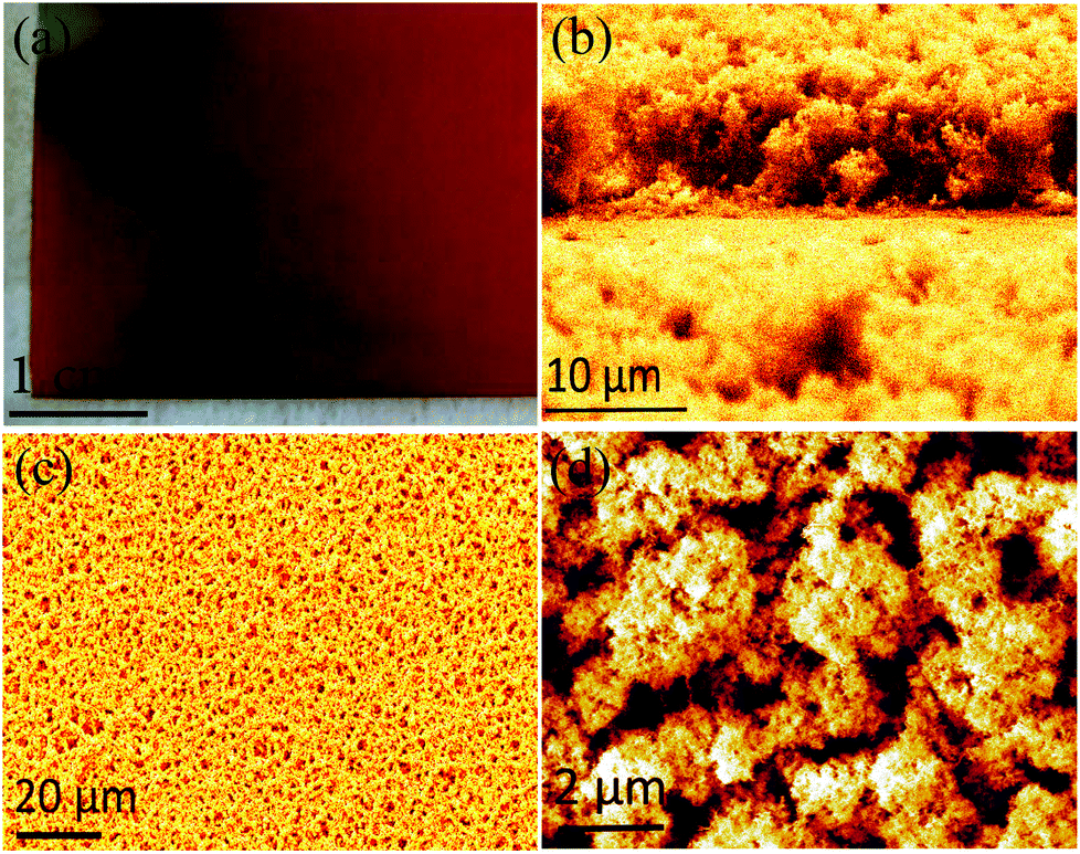 | ||
| Fig. 1 A photograph of a film of the Si NC material (a), SEM images of the cross-section (b) for the estimation of deposition rate, and from the top-view with a smaller (c) and a larger (d) magnification. | ||
HR-TEM was employed to observe the size and morphology of the NCs at larger magnifications. The Si powder was peeled off from the substrate and distributed in the ethanol solution. Then the Si NC suspension was dropped onto a copper grid pre-coated with a holey carbon film. The copper grid was transferred into the JEM-2100F field emission HR-TEM with an operating voltage of 200 kV. The HR-TEM images show two typical sizes for the Si NCs, i.e. small Si NCs in Fig. 2(a) and large Si NCs in Fig. 2(b). In the HR-TEM image in Fig. 2(a), many dense dots are shown clearly in the field of view. These small grains are Si NCs, as shown by the contrast difference between the Si NCs and the background. This shows that small Si NCs were formed and crystalized in the hot plasma. Well-isolated Si NCs with clear lattice fringes can be observed, while some surrounding Si tissue without lattice fringes remains in the amorphous state. It can be estimated that most of the small Si NCs have a diameter of 3–4 nm and the local density in the HR-TEM image is 4.0 × 1018 cm−3. Notice that these small NCs are collected on the substrate spots that are exactly below the holes in the SiH4 injection ring. Therefore, we believe that these small NCs were formed in the plasma beam and directly deposited on the substrate. However, free-standing larger NCs (diameter of dozens of nanometers) are also observed, as shown in Fig. 2(b). These large NCs are collected from other areas on the substrate. They have a larger average diameter due to recycling from the background volume into the plasma beam.26,27 The large NCs are regular spheres, with a native silicon oxide coating around them. Summarized, this bimodal size distribution from a typical sample is a result of the NCs being deposited directly from the plasma beam (2 nm < d < 10 nm) and recycling of NCs from the background volume into the plasma beam (20 nm < d < 50 nm).26,27 By varying the amount of SiH4 gas flow from 230, to 420 to 600 sccm (standard cubic centimeters per minute, other deposition parameters were fixed), 3 samples of free-standing Si NCs were deposited with different size distributions. The HR-TEM analysis confirmed that these samples have an average size for the large NCs of 27.2 ± 6.4 nm, 34.7 ± 16.2 nm and 41.3 ± 19.0 nm, respectively. The bimodal size distribution makes the ensembles of Si NCs studied in this paper unique in reference to typical Si NCs studied in the literature that have sizes smaller than 12 nm.28–34
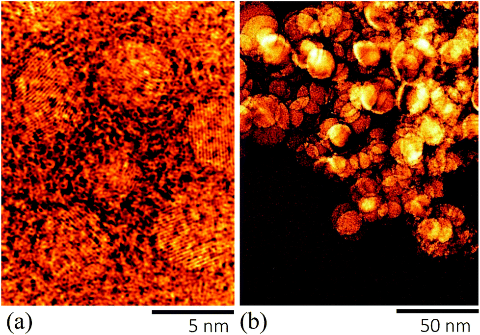 | ||
| Fig. 2 HR-TEM images of the small Si NCs embedded in an a-Si:H matrix collected from the substrate below the holes in the SiH4 injection ring in ETP-CVD (a), and the large free-standing Si NCs collected from other areas of the sample (b). | ||
The morphology of the nc-Si:H films deposited by PECVD is similar to that of the small NCs in Fig. 2(a), and these Si NCs are also embedded in an a-Si:H matrix. The Si NCs in an a-SiC:H matrix or nc-SiOx:H look similar to the nc-Si:H material, but they are embedded in the a-SiC:H and a-SiOx:H matrices, respectively.35
Raman laser heating of Si NCs
Raman spectroscopy was performed with a Renishaw inVia Micro-Raman microscope immediately after unloading the Si NC sample from the ETP-CVD chamber. The 100× lens sharply focused the visible light (λ = 514 nm) from an argon (Ar) ion laser on the samples. The estimated beam diameter of the spot on the sample was ∼4 μm. The intensity of the laser power could be varied by switching between filters having various transmissions (e.g., 1%, 5%, 10%, 50% and 100%). The laser power was measured using a handheld power meter (±8% accuracy). Under optimal focused conditions, the penetration depth of the light from the Ar ion laser in the bulk c-Si was ∼762 nm. Consequently, the penetration depth was deeper than 762 nm in porous samples of free-standing NCs.A conventional Raman setup is equipped with high-pass filters, which only allows the measurement of the Stokes (St) peak and blocks the anti-Stokes (ASt) peak ω0,ASt = −520.5 cm−1. However, the amplitude of the ASt TO mode is sensitive to the temperature of the NCs.31,36 To determine the temperature of the Si NCs, the ASt peak should be measured as well. Sharp band-stop filters at the excitation wavelength (514 nm in this work) were used to simultaneously measure the ASt and St peaks. Therefore, two identical Notch filters (Model NF03-514E-25, Laser 2000 Benelux CV Co.) were installed in our Renishaw Micro-Raman setup to fully filter out the excitation wavelength.
Results and discussion
Under mild laser illumination conditions, the shift of the first-order Si–Si mode peak of the small Si NCs (2 nm < d < 10 nm) in the Raman spectrum is lower by a few wavenumbers than the shift observed for the bulk c-Si ω0 = 520.5 cm−1, as observed by many others.5,23,37–39 In general this observation is attributed to phonon confinement, due to the presence of small NCs embedded in the hydrogenated amorphous Si (a-Si:H) environment (Fig. 2(a)). Assuming that this shift can be fully attributed to the quantum confinement effect, the average small NC size can be estimated from the anharmonic Raman softening according to this formula:40 | (1) |
Here, d (nm) stands for the diameter of the average NC, and C = 2.24 nm2 cm−1, and is a constant for the Si material. Δω is the absolute wavenumber (cm−1) difference between ω0 and the measured ω for the Si NCs, i.e., Δω = |ω0 − ω|. The average size can be determined from eqn (1). Tensile stress-induced effects were also reported to cause the red-shift.30,41 Tensile stress can be created if the Si NCs are significantly heated by laser absorption. Therefore, the above method works only when Si NCs are exposed to a low laser intensity and the materials have a good thermal conductivity to guarantee no significant heating of the NCs.
In our work, it will be shown that the large free-standing Si NCs can be significantly heated by intense laser illumination, and the quantum confinement effect is no longer the dominant mechanism for the red-shift of the first-order Si–Si mode peak. The large (20 nm < d < 50 nm) Si NCs are free-standing and therefore they have poor thermal conductivity properties.32 The large NCs are hardly physically interconnected and heat transfer is ineffective. During the measurements on such free-standing Si NCs with poor thermal conductivity, an interesting huge (Δω > 10 cm−1) red-shift and even melting of the Si NCs can be observed when they are exposed to an intensive and well-focused laser. Fig. 3(a)–(d) are pictures taken by the Philips SPC 900NC PC camera installed above the lens in the Renishaw Raman setup. The pictures show a sample after the measurements at four different laser illumination intensities and durations. In the employed measurement procedure, the free-standing Si NCs were intentionally and repeatedly heated on the same spot. Fig. 3(a) shows the image of the Si NCs after a 10 s exposure to a laser with a power of 69.3 μW. The material within the spot is almost unaffected compared to the as-deposited samples. When the laser power is raised to 346 μW, the sample is clearly affected by the exposure to the laser light. An affected zone with a diameter of ∼4–6 μm appears in the illumination spot, as illustrated in Fig. 3(b). This means that the layer of Si NCs in the spot is heated up to the extent that the Si NCs are melted. This melted Si “liquid” diffuses partly out of the illumination spot. If the laser power is further increased to 602 μW, the melting zone around the laser spot gets larger for an illumination exposure of 10 s, as shown in Fig. 3(c). In the following steps, even if this process is repeated 10 times, i.e. 100 s in total, the affected zone remains the same size and shape as in Fig. 3(c). What is interesting is that if the same spot is continuously illuminated by a 602 μW laser for 100 s only once, a volcano-shaped zone with a diameter of ∼8 μm and a ∼15 μm tail is observed, as shown in Fig. 3(d). Poborchii et al. reported that this volcano shape is caused by the “wind”, due to the simultaneous presence of a very high temperature gradient and decreasing absorption coefficients.25 However, this does not directly explain the difference from the effective intermittent exposure of 100 s, resulting in less melting of Si NCs compared to the uninterrupted exposure of 100 s. This indicates that due to the poor thermal conductivity of the free-standing Si NCs, it takes more than 10 s to reach a quasi-thermal equilibrium in the layer of Si NCs. These measurements demonstrate that light absorption by the free-standing Si NCs under the employed laser power can easily result in temperatures as high as their melting point.
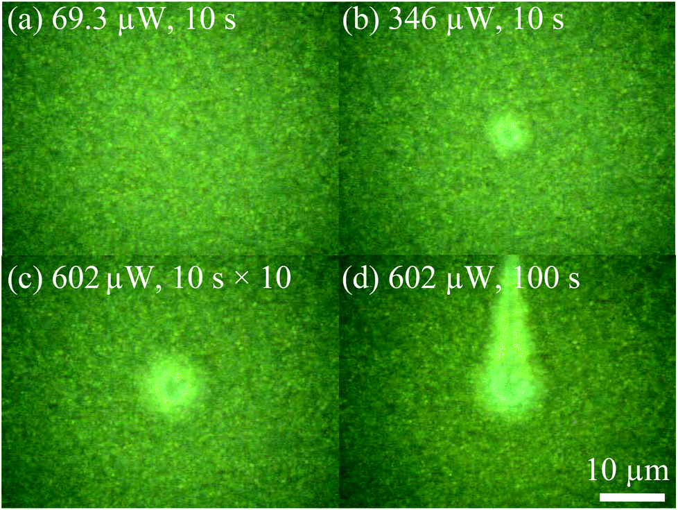 | ||
| Fig. 3 In situ photos of Si NCs after 10 s exposure to a laser with a power of 69.3 μW (a), the material remains unaffected compared to the as-deposited samples; an affected zone with a diameter of ∼5 μm appears in the illumination spot after 10 s exposure to a laser with a power of 346 μW (b); the Si “liquid” diffuses further after 10 s exposure to a laser with a power of 602 μW (c), and the sample remains unchanged if this is repeated 10 times; a volcano-shaped affected zone is formed after 100 s continuous exposure to a laser with a power of 602 μW (d). | ||
At first sight, it might be surprising that these Si NCs can melt (the melting point of c-Si is 1687 K at standard test conditions) when they are exposed to a power that is less than 1 mW. However, if we assume the laser power of 602 μW is equally distributed in a spot with a dL ≈ 4 μm diameter, the average power density is 4.79 × 10⁸ W m−2, which is equal to 47![[thin space (1/6-em)]](https://www.rsc.org/images/entities/char_2009.gif) 900 Suns in air mass 1.5 (AM 1.5, 1000 W m−2) conditions!
900 Suns in air mass 1.5 (AM 1.5, 1000 W m−2) conditions!
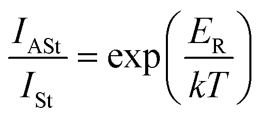
In order to estimate the temperature of the hot large Si NCs before melting under intensive illumination, we heated the Si NC sample step by step by increasing the Ar ion laser power from 3.3 to 16.5, 33, 165 and 330 μW. Fig. 4(a) shows that the St TO mode peak at 520.5 cm−1 red-shifts to 518, 517, 500 and even 495 cm−1, respectively. In addition, the full width at half maximum (FWHM) is widened greatly from 8.8 to 8.9, 9.5, 17.1 and 21.5 cm−1, respectively. The amplitude of the measured ASt TO mode at −520.5 cm−1 increases significantly with the enhancement of the laser power. To be more precise, both the ASt and St peaks increase significantly in intensity with laser power, however the ASt peaks increase in intensity more relative to the St peaks. The ASt peaks show a red-shift with the increasing laser power as well. To quantify the heating effects by the absorption of the laser light, we use the ratio of the ASt to St TO mode intensities to determine the temperature of the Si NCs.42 According to studies reported in the literature,31,33,36 the temperature of the Si NCs can be estimated by:
 | (2) |
 | ||
| Fig. 4 Anti-Stokes and Stokes TO mode peaks shift in the Raman spectra of the larger free-standing Si NCs with increasing Raman laser illumination (a). The TO mode red-shift and the full width at half maximum (FWHM) of the TO mode of the Stokes peak widening with the temperature enhancement (b). The dashed lines are guides for the eyes. | ||
Here, IASt/ISt is the ratio of the Anti-Stokes to Stokes (ASt to St) TO mode intensities, k is the Boltzmann constant, ER is the phonon energy (i.e., ER = hc/λexcitation − hc/λemission = hcω × 10−7), h and c are the Planck constant and light speed, respectively. ω is the Raman peak shift frequency expressed in cm−1. T, the temperature of the Si NCs during the laser heating, can then be determined from eqn (2).
The results in Fig. 4(a) reflect that the ratio of IASt/ISt increases with laser power, which means the large Si NCs were heated up by the absorption of the laser energy. The power of the probe laser is indicated on the left side of each curve. On the right side, the calculated temperature using eqn (2) is presented. The results show that the free-standing Si NCs can be heated from room temperature to as high as ∼953 K, when the laser power increases 100 times from 3.3 to 330 μW (∼263–26300 Suns). By further analyzing the data shown in Fig. 4(a), we find that the temperature of the illuminated free-standing Si NCs increases with the wavenumber enhancement of the red-shifts Δω, and simultaneously with the peak widening of the TO mode St peak, as shown by the FWHM enhancement in Fig. 4(b). This demonstrates that both Δω and FWHM are determined by the temperature of the Si NCs, and agrees with the findings in the literature.28,29,43
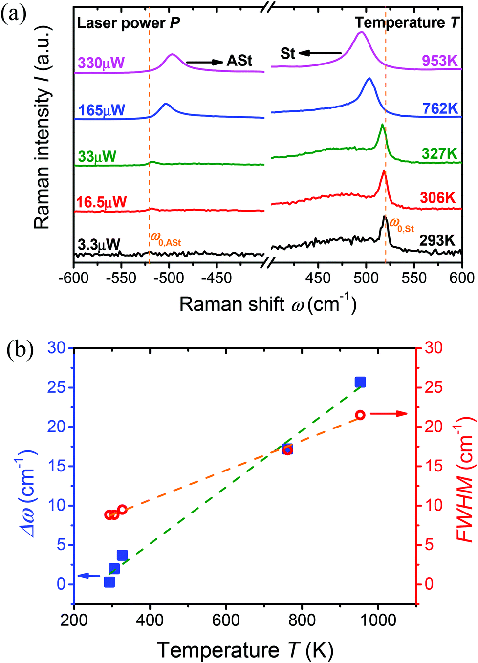
The question that remains is whether large Si NCs embedded in a host matrix can be significantly heated under the same illumination conditions as well? Therefore, the same laser heating Raman spectroscopy was done on the samples of Si NCs embedded in a matrix, such as Si NCs in a-SiC:H, nc-Si:H and nc-SiOx:H. Fig. 5 shows the temperatures of the Si-based materials when heated by the Ar ion laser. As shown, the free-standing Si NCs can be heated to temperatures up to ∼953 K. However, it is not easy to heat the other materials when they are embedded in a matrix. This demonstrates that the interconnection between the surfaces of the large Si NCs and the tissue of the host matrix results in good thermal conductivity. For example, Si NCs in an a-SiC:H matrix material (blue triangles in Fig. 5) can be heated up to ∼375 K illuminated by 330 μW. This temperature is slightly higher than for the Si NCs in nc-Si:H and nc-SiOx:H.
 | ||
| Fig. 5 Laser heating effects of several Si NC-based materials. Free-standing Si NCs are much easier to be heated than Si NCs embedded in various matrixes illuminated by intensive laser. The lines are guides for the eyes. | ||
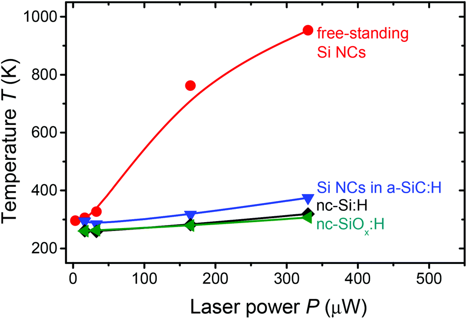
This comparison shows the unique properties of the large free-standing Si NCs. The fact that they are hardly physically interconnected limits the heat transfer between the particles. Another possible route for the free-standing particle to lose its heat is through blackbody radiation.34,44 We have observed signatures of such blackbody radiation from hot free-standing Si NCs. Fig. 6 shows the Raman spectra of a sample of free-standing Si NCs under large laser powers of 330 or even 660 μW. The presence of the St peaks in the spectra shows that the sample still contains solid Si NCs. However, the sample might contain a liquid Si phase as well. Furthermore, the red-shift is enormous: Δω ∼30 cm−1 (i.e., ω ∼490 cm−1). The background signals in the Raman spectra have a large tilt that even overrules the amplitude of the measured St peaks. Therefore it is not possible any more to accurately determine the temperature using eqn (2).
 | ||
| Fig. 6 Raman spectra of the large free-standing Si NCs under intensive (I = 330 and 660 μW) laser power. | ||
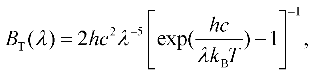
We claim that the background tilt reflects the blackbody radiation of the large Si NCs.34 The temperature of the large Si NCs gets so high that the intensity of blackbody radiation in the spectral range around the Raman laser, 519–542 nm (corresponds to 200 cm−1 ≤ ω ≤ 1000 cm−1), is similar to or higher than that of the St Raman peak. According to Planck's Law, the blackbody radiation of an object can be described as:
 | (3) |
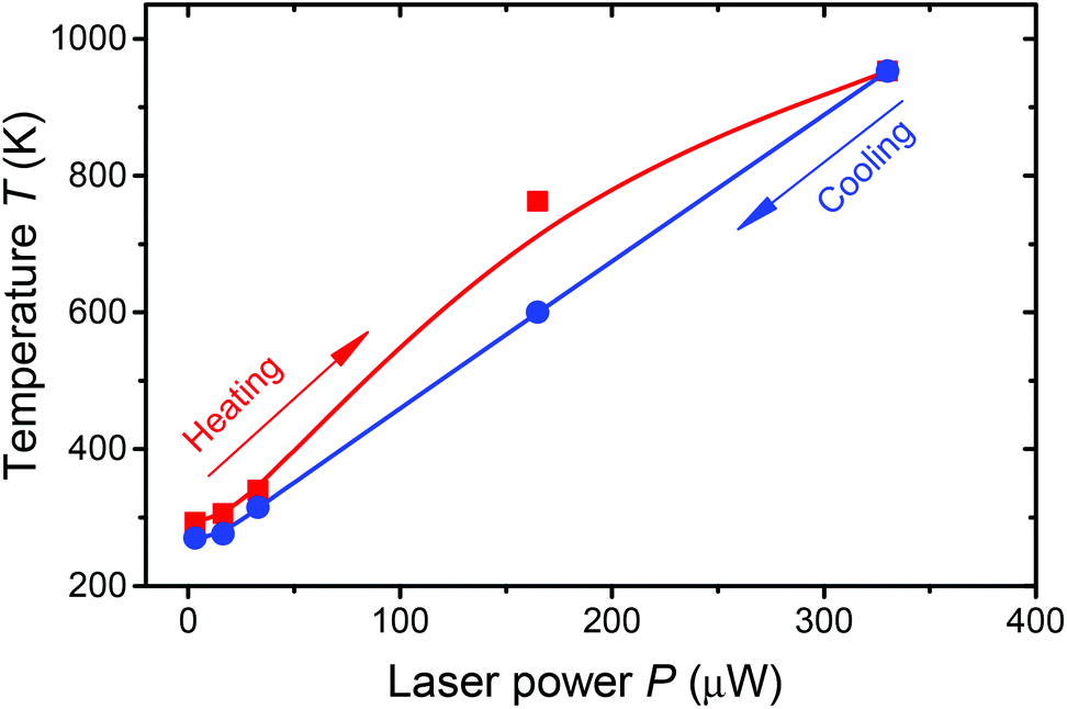
Another experiment was performed to test whether the Raman laser heating effects for large free-standing Si NCs were reversible and whether the morphology of the NCs was modified after the laser illumination. After the step by step increasing of the laser power on the same spot on the sample (results shown in Fig. 4), the laser power was decreased step by step. The temperature at every laser power (exposure time of 10 s) was determined again by the measured ratio of ASt to St TO mode intensities using eqn (2). The results are presented in Fig. 7. The TO mode positions and shapes during the “cooling” phase (data not shown here) are very similar to those illustrated in Fig. 4 at the same illumination conditions. This means that after reaching the highest temperature not all the Si is melted and Si NCs are still present in the layer. It can be noticed that during the “cooling” phase, the Si material can still be reasonably heated. However, it is also clear that the NCs left at the same spot in the “cooling” phase cannot reach the same temperature as in the initial “heating” phase. At an illumination power of 165 μW the temperature of the Si NCs in the “heating” phase is ∼762 K, while in the “cooling” phase it is significantly lower, ∼600 K. This temperature difference implies that the thermal conductivity of the ensemble of free-standing Si NCs has improved after going through the “heating” phase. A possible explanation could be that the aggregation of Si NCs or some melting of Si NCs has improved the physical interconnection of the NCs. We can conclude that the laser heating effects are to a large extent reversible, but the nature of the porous Si NC-based layer gets slightly modified under intensive laser-induced heating.
 | ||
| Fig. 7 Temperature comparison between the “heating” and “cooling” phases on the same spot in Si NC materials. | ||
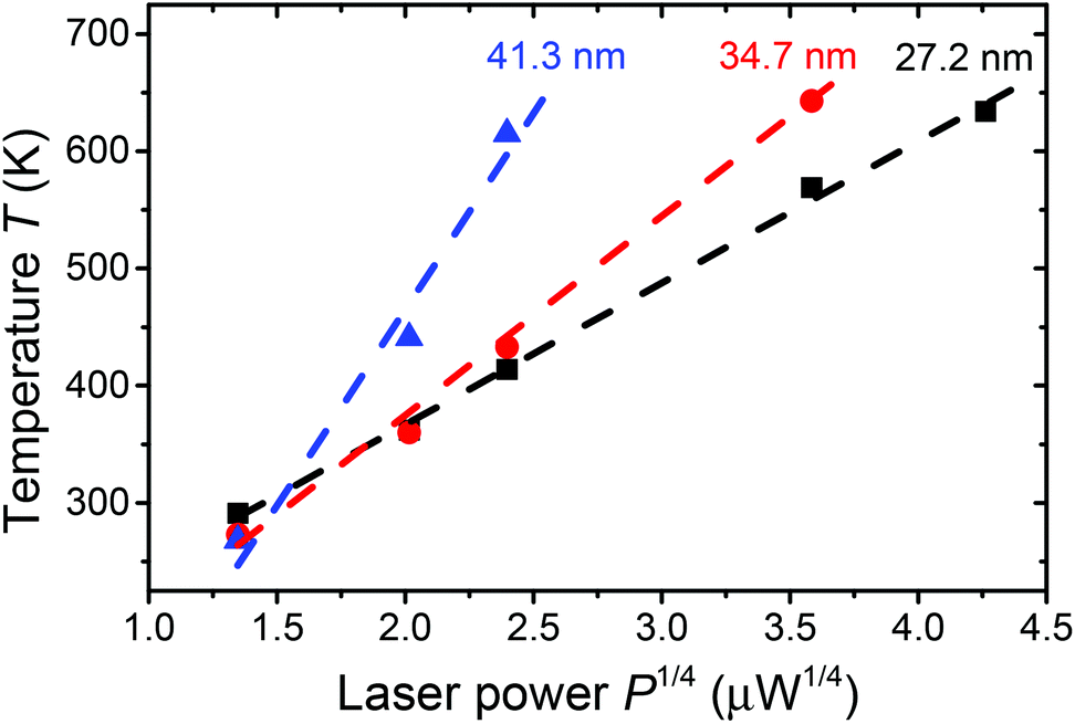
So far, we have demonstrated that large free-standing Si NCs can be significantly heated by laser illumination due to the poor thermal conductivity of these layers. In addition, we have observed that one of the heat loss mechanisms is blackbody radiation. If blackbody radiation was the dominant mechanism for free-standing NCs to lose their thermal energy, the equilibrium temperature under laser illumination should depend on the size of the NCs. In the final part of this paper, we will study whether this is indeed the case. A simplified model is established for this study. We assume that the thermal conductivity between the neighboring Si NCs can be neglected and that the laser penetration depth in c-Si (∼762 nm) is much larger than the typical average diameter (d) of the Si NCs (20 < d < 50 nm). The laser intensity I is the laser power P divided by the laser spot size on the sample, I ∼ P/(πdL2/4), with dL ≈ 4 μm the diameter of the spot size. The power absorbed by one single NC (Pabs) is proportional to the NC volume and can be estimated by Pabs ∼ (πd3/6)αP/(πdL2/4) ∼ Pd3, with α the absorption coefficient of Si at 514 nm. The radiation at thermal equilibrium from one single NC (Pirr) is estimated by the Stefan–Boltzmann Law, Pirr ∼ σT4πd2 ∼ T4d2, where σ stands for the Stefan–Boltzmann constant. At thermal equilibrium, the thermal generation and thermal losses of the Si NCs are equal, i.e., Pabs ≈ Pirr. Under these conditions T, d, and I are related for each specific sample as follows:
| T ∼ d1/4P1/4(T, d) | (4) |
So in the case that blackbody radiation is dominant, we can expect a relation between T and P given by eqn (4). We have measured this dependence for three samples of free-standing NCs with different average diameters for the large particles, d = 27.2 ± 6.4, 34.7 ± 16.2 and 41.3 ± 19.0 nm. This data is presented in Fig. 8. The results confirm that temperature can be simulated with a T ∼ P1/4 dependence (for each specific sample, the average diameter d is a fixed value). This implies that indeed the thermal conductivity of the large Si NCs can be neglected compared to thermal radiation. Furthermore, eqn (4) predicts that the slope of the T ∼ P1/4 dependence increases with the average size of the large Si NCs. This is in agreement with the results shown in Fig. 8. The larger NCs (sample with d = 41.3 nm) are easier to be heated than the smaller ones (samples with d = 34.7 and 27.2 nm) when the same amount of laser power is used. The trend in Fig. 8 additionally explains why the small Si NCs (if they were fully free-standing) do not significantly heat up. Considering small Si NCs with a diameter of 4 nm, the Si NCs would only heat up to ∼370 K for the highest laser power shown in Fig. 8.
 | ||
| Fig. 8 Temperatures determined from the Raman laser heating effects show a dependence on the average sizes of free-standing Si NCs. T ∼ P1/4 fitting of each sample is illustrated by the dashed curves. | ||
Conclusions
In this paper, the laser-induced heating effects were studied in bimodal size-distributed Si NCs using Raman spectroscopy. The Si NCs were fabricated by ETP-CVD, and the morphology of the NCs was characterized by SEM and HR-TEM. Under low intensity illumination at a wavelength of 514 nm, the typical quantum confinement effects for small Si NCs (diameter of 2–10 nm) were observed. The TO mode of the first order Si–Si peak red-shifted a few wavenumbers in reference to the bulk c-Si at 520.5 cm−1 due to the quantum confinement effect. The average diameter of these small Si NCs could be estimated according to the amount of this red-shift. However, if the free-standing Si NCs were illuminated by an intensive Ar ion laser, the thermal heating effects of the large Si NCs (diameter of 20–50 nm) became the dominant mechanism for the TO mode shift in the Raman spectrum. A huge red-shift up to ∼25.7 cm−1 and a peak widening of ∼12.7 cm−1 was observed as a result of the lattice expansion in the Si NCs. The melting of large Si NCs illuminated by intensive laser was monitored by a camera installed in the Raman setup. The temperatures of the heated Si NCs were determined using the ratio of Anti-Stokes to Stokes TO mode intensities. The large free-standing Si NCs could be heated as hot as ∼953 K by a well-focused laser with a power of 330 μW. In contrast, Si NCs in various matrixes were fabricated by PECVD. These samples could hardly be heated using the same amount of laser power due to their good thermal conductivity. If the large free-standing Si NCs were further heated, the intensity of the blackbody radiation in the Raman spectrum started to compete with that of the TO mode. When the materials were in a mixed phase of liquid and solid NCs, the temperatures were estimated to be in the range of 1005–1015 K according to Planck's Law. The laser heating effects were confirmed to be reversible to a large extent, but the nature of the material was slightly modified after intensive laser illumination. A simplified model of the heating effects of large Si NCs was established in order to study the size dependence of the heated free-standing Si NCs with increasing laser power.Acknowledgements
Financial support from the VIDI project granted to Dr Arno H.M. Smets by NWO-STW is gratefully acknowledged. Scientific discussions with Dr Jing Wang (Tsinghua University, China) and Dr Leonid Khriachtchev (University of Helsinki, Finland) are appreciated. The authors are much obliged for the daily technical equipment support from our colleagues Martijn Tijssen (ETP-CVD) and Stefaan G.M. Heirman (Raman laser alignment). Dr Karol Jarolimek (Si NCs in a-SiC:H) and Dr Pavel Babal (nc-SiOx:H) are thanked for the deposition of the reference samples.Notes and references
- M. A. Reed, J. N. Randall, R. J. Aggarwal, R. J. Matyi, T. M. Moore and A. E. Wetsel, Phys. Rev. Lett., 1988, 60, 535–537 CrossRef CAS PubMed.
- C. W. Jiang and M. A. Green, J. Appl. Phys., 2006, 99, 114902 CrossRef.
- L. F. Sun, J. J. Choi, D. Stachnik, A. C. Bartnik, B. R. Hyun, G. G. Malliaras, T. Hanrath and F. W. Wise, Nat. Nanotechnol., 2012, 7, 369–373 CrossRef CAS PubMed.
- B. Sun, P. Munroe and G. X. Wang, Sci. Rep., 2013, 3, 2247 Search PubMed.
- L. Han, J. Wang and R. Liang, 35th IEEE Photovoltaic Specialist Conference, 2010, pp. 3338–3342.
- L. Han, J. Wang and R. Liang, Adv. Mater. Res., 2012, 383–390, 6270–6276 CAS.
- Y. Tachibana, L. Vayssieres and J. R. Durrant, Nat. Photonics, 2012, 6, 511–518 CrossRef CAS.
- W. Shockley and H. J. Queisser, J. Appl. Phys., 1961, 32, 510–519 CrossRef CAS.
- T. Trupke, M. A. Green and P. Wurfel, J. Appl. Phys., 2002, 92, 1668–1674 CrossRef CAS.
- D. Timmerman, I. Izeddin, P. Stallinga, I. N. Yassievich and T. Gregorkiewicz, Nat. Photonics, 2008, 2, 105–109 CrossRef CAS.
- F. F. Abdi, L. Han, A. H. M. Smets, M. Zeman, B. Dam and R. van de Krol, Nat. Commun., 2013, 4, 2195 Search PubMed.
- L. Han, F. F. Abdi, P. Perez Rodriguez, B. Dam, R. van de Krol, M. Zeman and A. H. M. Smets, Phys. Chem. Chem. Phys., 2014, 16, 4220–4229 RSC.
- L. Han, F. F. Abdi, R. van de Krol, R. Liu, Z. Huang, H.-J. Lewerenz, B. Dam, M. Zeman and A. H. M. Smets, ChemSusChem, 2014, 7, 2832–2838 CrossRef CAS PubMed.
- L. Han, I. A. Digdaya, T. W. F. Buijs, F. F. Abdi, Z. Huang, R. Liu, B. Dam, M. Zeman, W. A. Smith and A. H. M. Smets, J. Mater. Chem. A, 2015, 3, 4155–4162 CAS.
- L. Han, F. F. Abdi, R. van de Krol, B. Dam, M. Zeman and A. H. M. Smets, 40th IEEE Photovoltaic Specialist Conference, 2014, pp. 3083–3086.
- W. D. A. M. de Boer, D. Timmerman, K. Dohnalova, I. N. Yassievich, H. Zhang, W. J. Buma and T. Gregorkiewicz, Nat. Nanotechnol., 2010, 5, 878–884 CrossRef CAS PubMed.
- A. G. Aberle, S. Glunz and W. Warta, J. Appl. Phys., 1992, 71, 4422–4431 CrossRef CAS.
- W. H. Chang, A. T. Chou, W. Y. Chen, H. S. Chang, T. M. Hsu, Z. Pei, P. S. Chen, S. W. Lee, L. S. Lai, S. C. Lu and M. J. Tsai, Appl. Phys. Lett., 2003, 83, 2958–2960 CrossRef CAS.
- B. C. Connelly, G. D. Metcalfe, H. E. Shen and M. Wraback, Appl. Phys. Lett., 2010, 97, 251117 CrossRef.
- D. Gammon, E. S. Snow, B. V. Shanabrook, D. S. Katzer and D. Park, Phys. Rev. Lett., 1996, 76, 3005–3008 CrossRef CAS PubMed.
- J. Y. Marzin, J. M. Gerard, A. Izrael, D. Barrier and G. Bastard, Phys. Rev. Lett., 1994, 73, 716–719 CrossRef CAS PubMed.
- A. L. Patterson, Phys. Rev., 1939, 56, 978–982 CrossRef CAS.
- Z. F. Sui, P. P. Leong, I. P. Herman, G. S. Higashi and H. Temkin, Appl. Phys. Lett., 1992, 60, 2086–2088 CrossRef CAS.
- Y. Kanemitsu, H. Uto, Y. Masumoto, T. Matsumoto, T. Futagi and H. Mimura, Phys. Rev. B: Condens. Matter, 1993, 48, 2827–2830 CrossRef CAS.
- V. Poborchii, T. Tada and T. Kanayama, J. Appl. Phys., 2005, 97, 104323 CrossRef.
- I. Dogan, N. J. Kramer, R. H. J. Westermann, K. Dohnalova, A. H. M. Smets, M. A. Verheijen, T. Gregorkiewicz and M. C. M. van de Sanden, J. Appl. Phys., 2013, 113, 134306 CrossRef.
- I. Dogan and M. C. M. van de Sanden, J. Appl. Phys., 2013, 114, 134310 CrossRef.
- G. Faraci, S. Gibilisco and A. R. Pennisi, Phys. Lett. A, 2009, 373, 3779–3782 CrossRef CAS.
- G. Faraci, S. Gibilisco and A. R. Pennisi, Phys. Rev. B: Condens. Matter, 2009, 80 Search PubMed.
- T. Nikitin, L. Khriachtchev, M. Rasanen and S. Novikov, Appl. Phys. Lett., 2009, 94, 173116 CrossRef.
- L. Khriachtchev, M. Rasanen and S. Novikov, J. Appl. Phys., 2006, 100, 053502 CrossRef.
- L. Khriachtchev, J. Electrochem. Soc., 2012, 159, K21–K26 CrossRef CAS.
- L. Khriachtchev, M. Rasanen and S. Novikov, Appl. Phys. Lett., 2006, 88, 013102 CrossRef.
- L. Khriachtchev, M. Rasanen and S. Novikov, Appl. Phys. Lett., 2005, 86, 141911 CrossRef.
- P. Babal, PhD thesis, TU Delft, 2014, in press.
- M. Balkanski, R. F. Wallis and E. Haro, Phys. Rev. B, 1983, 28, 1928–1934 CrossRef CAS.
- G. Conibeer, M. Green, E. C. Cho, D. Konig, Y. H. Cho, T. Fangsuwannarak, G. Scardera, E. Pink, Y. D. Huang, T. Puzzer, S. J. Huang, D. Y. Song, C. Flynn, S. Park, X. J. Hao and D. Mansfield, Thin Solid Films, 2008, 516, 6748–6756 CrossRef CAS.
- S. K. Gupta and P. K. Jha, Solid State Commun., 2009, 149, 1989–1992 CrossRef CAS.
- L. Sirleto, M. A. Ferrara, T. Nikitin, S. Novikov and L. Khriachtchev, Nat. Commun., 2012, 3, 1220 CrossRef PubMed.
- G. X. Cheng, K. J. Chen, W. Zhang, H. Xia and X. K. Zhang, Phys. Status Solidi A, 1992, 129, 421–434 CrossRef CAS.
- A. A. D. T. Adikaari and S. R. P. Silva, J. Appl. Phys., 2005, 97, 114305 CrossRef.
- A. Compaan, M. C. Lee and G. J. Trott, Phys. Rev. B, 1985, 32, 6731–6741 CrossRef CAS.
- G. Faraci, A. R. Pennisi, A. Alberti, R. Ruggeri and G. Mannino, Sci. Rep., 2013, 3 Search PubMed.
- J. Costa, P. Roura, J. R. Morante and E. Bertran, J. Appl. Phys., 1998, 83, 7879–7885 CrossRef CAS.
- S. K. Deb, M. Wilding, M. Somayazulu and P. F. McMillan, Nature, 2001, 414, 528–530 CrossRef CAS PubMed.
- A. N. Goldstein, Appl. Phys. A: Mater. Sci. Process., 1996, 62, 33–37 CrossRef.
- K. Nishio, T. Morishita, W. Shinoda and M. Mikami, Phys. Rev. B: Condens. Matter Mater. Phys., 2005, 72, 245321 CrossRef.
| This journal is © The Royal Society of Chemistry 2015 |