
 Open Access Article
 This Open Access Article is licensed under a
 Creative Commons Attribution 3.0 Unported Licence
Non-exponential resistive switching in Ag2S memristors: a key to nanometer-scale non-volatile memory devices
Agnes
Gubicza
*ab,
Miklós
Csontos
a,
András
Halbritter
ab and
György
Mihály
ab
aDepartment of Physics, Budapest University of Technology and Economics, Budafoki ut 8, 1111 Budapest, Hungary. E-mail: gubicza@dept.phy.bme.hu
bMTA-BME Condensed Matter Research Group, Budafoki ut 8, 1111 Budapest, Hungary
First published on 4th February 2015
Abstract
The dynamics of resistive switchings in nanometer-scale metallic junctions formed between an inert metallic tip and an Ag film covered by a thin Ag2S layer are investigated. Our thorough experimental analysis and numerical simulations revealed that the resistance change upon a switching bias voltage pulse exhibits a strongly non-exponential behaviour yielding markedly different response times at different bias levels. Our results demonstrate the merits of Ag2S nanojunctions as nanometer-scale non-volatile memory cells with stable switching ratios, high endurance as well as fast response to write/erase, and an outstanding stability against read operations at technologically optimal bias and current levels.
Future technological developments in non-volatile resistance switching random access memory (ReRAM) applications1–3 exceeding the limitations of present-day flash devices4 are expected to comply with the basic requirements of a small size for a high data storage density as well as fast read and write operations performed at reasonably low voltages and easily detectable current levels. Further important criteria include high endurance against several writing cycles and a long retention time,5 which greatly rely on the long-term mechanical and electrical stability of the corresponding ON and OFF states. Moreover, it is also a key issue that such passive circuit elements exhibit a strongly non-linear response function, so that the device is stable against low-level read-out signals and, at the same time, responds quickly to write operations carried out at higher biases.
Tunable, nanometer scale junctions formed between metallic electrodes by reversible solid state electrochemical reactions represent extremely promising candidates to satisfy the above criteria.1,6–17 The resistive state of such a memory element, called memristor,18 is altered by biasing the device above its writing threshold (Vth). Readout is performed at lower signal levels which preserve the stored information.
Previous studies on the dynamical properties of memristive systems6,9,17,19–34 mostly focused on the formation and complete rupture of metallic filaments in solid state ionic conductors, giving rise to extremely high ROFF/RON ratios at practically insulating ROFF and RON ≈ h/2e2 = 12.9 kΩ resistance values, the latter corresponding to atomic sized contacts. While the near-equilibrium conditions of low ionic and tunneling currents facilitated the identification of the underlying microscopic mechanisms in this regime, fundamental RC limitations only allowed the exploration of narrower segments in the time domain.
Our previous experiments35 have shown that suitably prepared, nanometer scale junctions utilizing a 30 nm thick layer of the ionic conductor Ag2S sandwiched between Ag and PtIr electrodes are capable of reproducible, nanosecond timescale switching operation at room temperature exhibiting ROFF/RON ratios of 2–10. Resistive switching takes place via metallic channels of diameters in the range of 2–5 nm which are subject to electric fields of the order of 106 V cm−1 and current densities of 1010 A cm−2. The technologically optimal, metallic ON and OFF state resistance values of about 1 kΩ are fully compatible with present-day CMOS standards. Moreover, the considerably lower writing (read-out) voltages of a few 100 mV (10 mV) applied for two orders of magnitude shorter times offer a significantly decreased power consumption.
Here we discuss the dynamics of the resistance change during such resistive switchings, representing a so far relatively unexplored area in memristor research. We demonstrate stable switching ratios over >104 writing cycles and the stability of the stored information. We show that the switchings can simultaneously exhibit fast and slow variations over more than eight orders of magnitude in time with characteristic time scales highly depending on the biasing conditions. This enables the utilization of Ag2S based nanojunctions in non-volatile memory applications. The transition between two different states is found to be non-exponential in time reminiscent of the variation of the synaptic potential36–38 also responsible for the short- and long-term memory of the human brain.20,39 The latter behaviour has been successfully accounted for by numerical simulations based on an empirical master equation.
During sample fabrication an 80 nm thick Ag layer was deposited onto a Si substrate followed by a 5 minutes long sulfurisation. The S diffused into the Ag layer, forming an approximately 30 nm thick Ag2S layer on top of the Ag.40 Nanometer scale junctions were created by gently touching the Ag2S surface with a mechanically sharpened PtIr tip in an STM geometry. The Vdrive voltage output of a low output impedance (5 Ω) arbitrary waveform generator was acting on the memristive junction and on the serial resistor Rs while the Vbias voltage drop on the junction was monitored using an oscilloscope as shown in the left inset of Fig. 1(a). By convention, a positive bias corresponds to positive voltage applied to the Ag layer with respect to the PtIr electrode. All measurements were performed at room temperature.
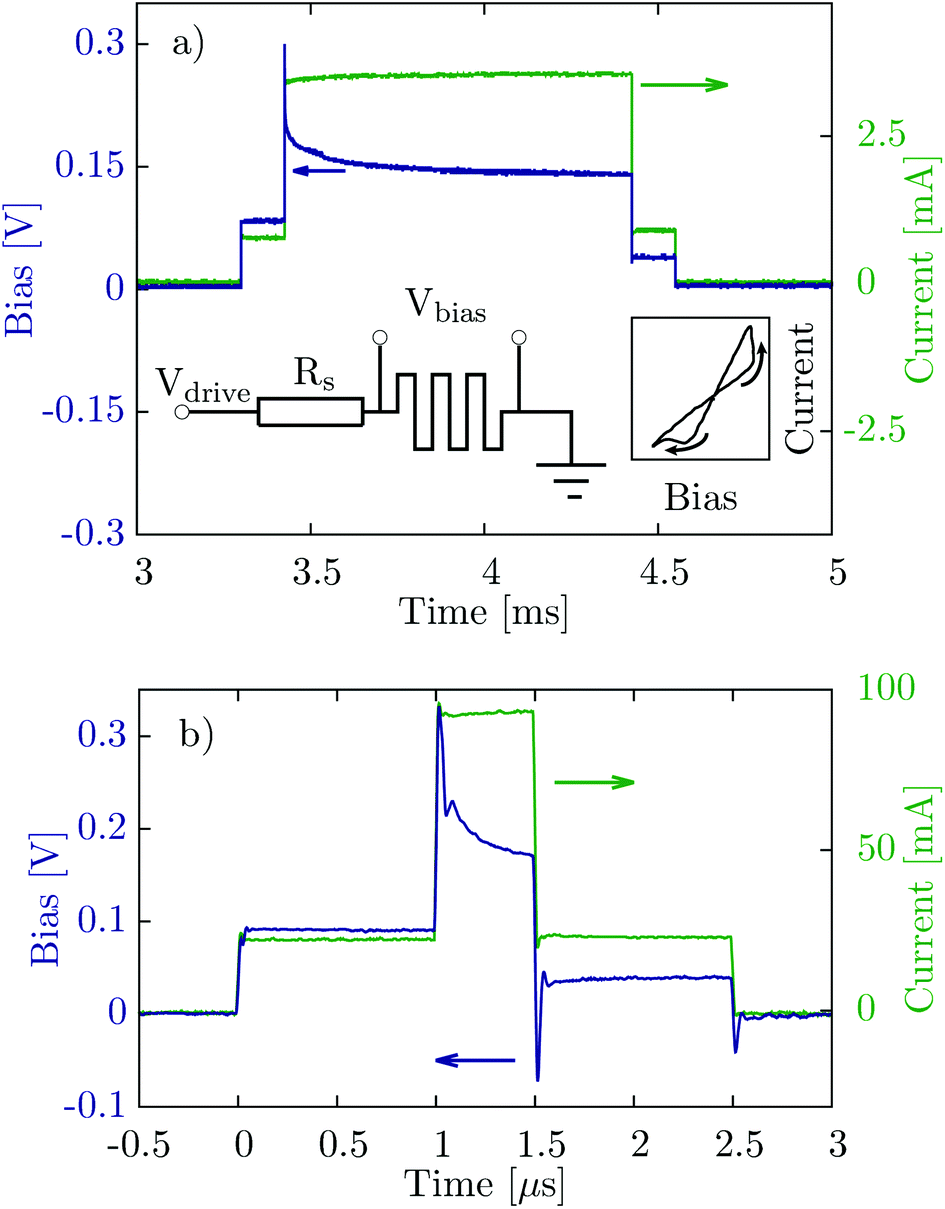 | ||
| Fig. 1 Resistive switchings initiated by 1 ms (a) and 500 ns (b) long voltage pulses. The positive bias corresponds to positive voltage applied to the Ag layer with respect to the PtIr tip. The blue curves represent the voltage drop on the junction. The green traces correspond to the current flowing through the device. The insets show typical I–V characteristics acquired within 1 ms as well as the electrical circuit diagram of the biasing setup. The 1 ms long voltage pulse was applied with Rs = 330 Ω on a junction exhibiting ROFF = 110 Ω and RON = 41 Ω. During the 500 ns pulse Rs = 50 Ω was used in series with ROFF = 5 Ω and RON = 2 Ω. | ||
A typical current–voltage (I–V) trace recorded within 1 ms is illustrated in the right inset of Fig. 1(a). At low bias voltages the initial OFF state resistance ROFF is measured. With increasing Vbias to Vth = 200 mV, a reconfiguration takes place, resulting in a drop in the junction's resistance from ROFF = 70 Ω to RON = 38 Ω. Lowering Vbias preserves the RON ON state resistance until a negative threshold of −300 mV is reached where the initial OFF state is restored. The direction of the resulting hysteresis loop is indicated by the arrows in the inset.
Resistive switchings can also be initiated by voltage pulses as demonstrated in Fig. 1(a) and (b) for different pulse durations in two representative junctions. In each case the junction is prepared in its higher resistance OFF state by a high amplitude negative voltage pulse of Vdrive = −1.3 V [Fig. 1(a)] and −4.5 V [Fig. 1(b)] (not shown). ROFF is measured at a low positive read-out voltage. This is followed by a high amplitude positive pulse (Vdrive = +1.3 V and +4.5 V, respectively) to switch the device to its lower resistance ON state. Again, a low read-out voltage is applied to determine RON in the final state. Note that due to Rs > ROFF the observed change is more dominant in the voltage response of each device, compared to its current variation. While Fig. 1(a) demonstrates that the junction exhibits a significant resistance change even at the time scale of the 1 ms long switching pulse, a three orders of magnitude faster operation is exemplified in Fig. 1(b) where a resistance change by a factor of ≈2 is achieved within 500 ns. Moreover, our previous experiments showed that resistive switchings can be initiated by voltage pulses as short as 500 ps.35 These observations indicate that fast and slow switching processes can co-exist in Ag2S based nanojunctions. In the main part of this paper we exploit this unique behaviour by a thorough analysis of the switching characteristics under various biasing conditions.
The colour map of Fig. 2(a) displays the ROFF/RON ratio deduced from the zero-bias slopes of the >104 individual I–V traces acquired on a representative, stable device at different fdrive frequencies and V0drive amplitudes of the driving triangle signal and using Rs = 51 Ω. By gradually increasing V0drive above a switching threshold the ROFF/RON ratio exceeds unity. We have repeatedly increased V0drive at various driving frequencies until ROFF/RON = 4 was achieved. The data show a clear logarithmical increase in the switching threshold towards higher frequencies. The regions of constant α = ROFF/RON ratios can be well approximated by the formula:
| Vdrive = a·lg(fdrive) + b, | (1) |
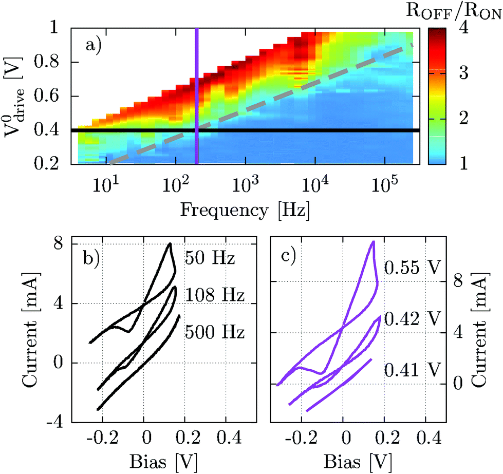 | ||
| Fig. 2 (a) Resistance ratio α = ROFF/RON as a function of the driving frequency and amplitude. The dashed line is a guide to the eye visualizing the empirical relation of eqn (1) describing the α = constant regions. (b) Selected I–V traces taken at V0drive = 0.4 V and various frequencies along the black line indicated in (a). (c) I–V traces taken at fdrive = 200 Hz with different amplitudes along the magenta line in (a). The curves in (b) and (c) are vertically shifted for clarity. | ||
Our data reveal that in spite of the statistical nature of the microscopic processes responsible for the observed resistive switching, the ROFF/RON ratio is a monotonous function of the driving amplitude and one needs larger V0drive to initiate faster resistance changes, while at a certain frequency a well established threshold voltage sets in. Note that increasing V0drive results in a larger resistance change, while the maximal Vbias voltage drop on the memristive element is locked to the threshold voltage at increasing device currents (quasi-vertical part of the I–V curve). We found that different junctions exhibit a qualitatively similar logarithmic relation between the threshold amplitude and the frequency; however, the actual parameters of this relation may moderately vary from device to device.
In order to gain a more detailed insight into the dynamics of the resistive switchings we monitored the R(t) resistance of the junction over six decades in the time domain with a resolution of 2 μs during a 1 s positive rectangular voltage pulse for various Vdrive amplitudes, Rs series resistors and ROFF initial resistances. Fig. 3(a) shows three representative experimental R(t) traces on a log–log scale. The black curve corresponding to a junction with ROFF = 2.2 kΩ shows a gradual variation over more than 5 orders of magnitude in time, whereas the resistance corresponding to ROFF = 167 Ω (green curve) only changes during the last one and a half decade. It is to be emphasized that none of the three curves can be properly described by introducing a single time constant. While, for instance, an exponential fit to the initial part of the black trace provides a time constant of 10 μs, R(t) around the falling edge of the Vdrive pulse can be best described by a time constant of 10 s. Consistent with the tendency shown in Fig. 2, this markedly different behaviour is attributed to the different Vbias(0) = VdriveROFF/(Rs + ROFF) initial voltage drops acting on the device, i.e., shorter characteristic time scales can be achieved at higher Vbias(0) values. As R(t) is decreasing toward the final RON resistance, Vbias(t) also undergoes a downscaling in the fashion of the above formula, resulting in a further slowdown of the resistance change which becomes observable even up to seconds. We point out that the former issue, i.e., the fast (slow) resistance change at high (low) Vbias, is inevitable for fast write/erase (slower, non-volatile read-out) operations in ReRAM applications. The gradual transition behavior from the OFF to the ON state under a constant voltage application is markedly different from the sharp transition observed in atomic switches.41 This is attributed to the role of multiple degrees of freedom in our system consisting of metallic channels of 2–5 nm in diameter35 instead of single atoms in the narrowest cross-section of the junction. We speculate that the dominating driving force of the resistance change is still electric field driven activated ionic transport, giving rise to the expansion/shrinkage of the metallic conduction channel, which is determined by its local asymmetry around the narrowest cross-section of the junction. However, the considerable self-heating of the junction and the electron wind forces due to high current densities may also play a role in the resistive switching. Identifying the detailed microscopic mechanisms is the subject of ongoing molecular dynamical simulations.
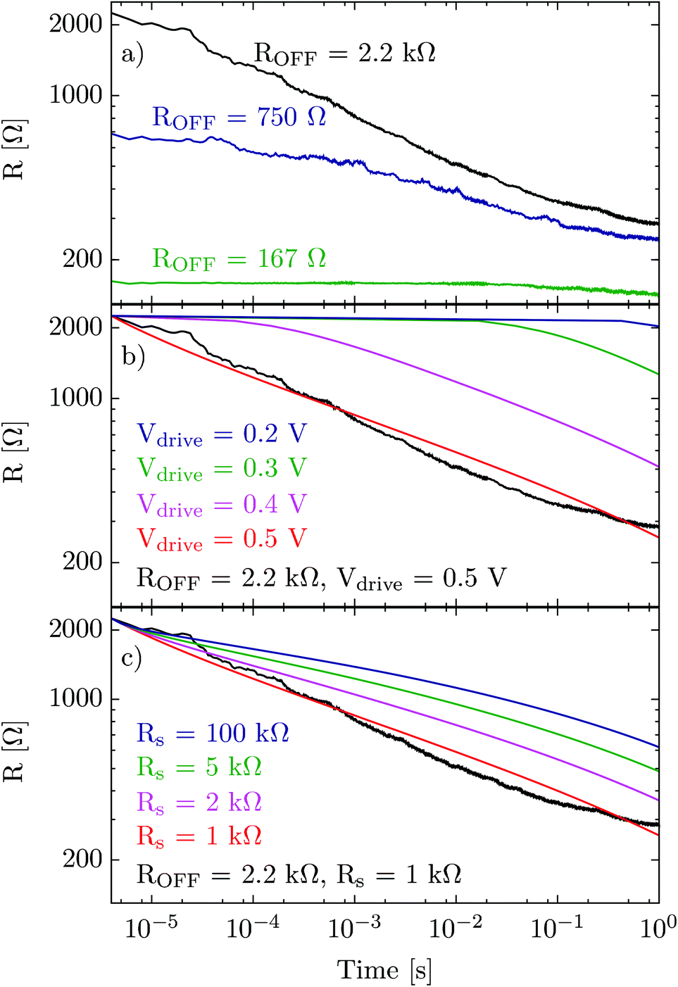 | ||
| Fig. 3 (a) Junction resistances R(t) recorded during 1 s long rectangular voltage pulses of different amplitudes at various ROFF initial resistances. Rs = 1 kΩ, Vdrive = 0.5 V (black), Rs = 1330 Ω, Vdrive = 1 V (blue), Rs = 1330 Ω, and Vdrive = 0.9 V (green). (b) The results of numerical simulations for R(t) at varying Vdrive at ROFF = 2.2 kΩ and Rs = 1 kΩ. (c) Similar simulations performed at varying Rs and Vdrive at identical initial Vbias(0) = 0.35 V and ROFF = 2.2 kΩ. The black lines in (b) and (c) represent the data shown in (a) with ROFF = 2.2 kΩ, Rs = 1 kΩ and Vdrive = 0.5 V. | ||
The observed behaviour was also accounted for by a time-dependent numerical simulation demonstrating that due to their common origin the time dependence of the resistance change during a voltage pulse [Fig. 3(a)] is necessarily consistent with the bias and frequency dependence of the switching ratios, as determined from complete I–V traces (Fig. 2). Based on the empirical logarithmic relation deduced from the data shown in Fig. 2(a) we assume that a resistance change of α = R(t)/R(t + Δt) takes place within a characteristic time of Δt = 10−[Vbias−b]/a in the fashion of eqn (1), where Vbias = Vdrive·R(t)/(R(t) + Rs) is the actual voltage drop acting on the junction. During the numerical implementation the initial resistance value R(1) was chosen to be equal to ROFF at the time t(1) = 0. The Δt(n + 1) time required to achieve the next resistance value R(n + 1) = R(n)/α was determined by the above formulae in each iteration step.
The results of the simulations performed at various Vdrive and constant ROFF and Rs as well as at various Rs but identical Vbias(0) values and at constant ROFF are illustrated in Fig. 3(b) and (c), respectively. The black experimental trace of Fig. 3(a) characterized by the same parameters as the red simulated line is re-plotted in Fig. 3(b) and (c) for comparison. It is evident that our simulation not only describes the selected experimental time traces by using exclusively pre-determined empirical values but the two sets of curves also properly account for the observed tendencies attributed to the complementary effects of changing Vbias(0) and ROFF/Rs. Note that the parameters a, b and α used to construct the traces of Fig. 3(b) and (c) correspond to a different junction and are therefore different from those describing the data shown in Fig. 2(a) within a factor of two.
The above described emergence of the different time scales during the switching process can be further visualized by mixing a small amplitude, high frequency modulation with a slowly varying, higher amplitude triangular driving signal and utilizing lock-in detection to determine the finite bias current-to-voltage response of the junction. This technique enables the separation of the characteristic time scales governing the resistance change of the junction. If the change is fast enough to follow the AC modulation, the lock-in detected signal is expected to return the dI/dVbias derivative of the I–V curve. In contrast, if the lock-in frequency exceeds the speed of the internal processes in the system, the junction is unable to change its resistance during one period of the lock-in excitation. Hence the latter is not expected to detect the differential resistance but only the actual Ohmic resistance of the junction.
Fig. 4 shows the result of the simultaneous AC and DC detection of a typical I–V trace. Both the AC and DC components were applied over Rs ≫ ROFF serial resistors adding a Vacbias ≈ 1 mV, f = 1 kHz modulation to the DC trace recorded within 1 s. The red line in Fig. 4 displays a DC I–V trace while the slopes of the black dashes shown at selected finite bias values represent the harmonic response measured by the lock-in amplifier. Whereas in the well defined ON and OFF states both the AC and DC methods accurately return the actual dI/dVbias values, it is evident that under these conditions the internal time-scale of the system was too long to follow the AC modulation during the resistive switchings, giving rise to a harmonic response corresponding to the Ohmic resistance of the junction. It has to be added that a qualitatively similar behaviour was found in various junctions tested in the 1 kHz < f < 100 kHz lock-in frequency domain, in agreement with the quantitative predictions deduced from Fig. 2.
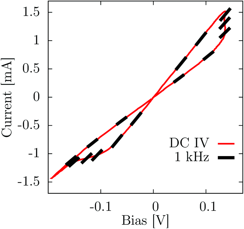 | ||
| Fig. 4 I–V trace recorded at a slow bias signal of f = 1 Hz (red). The results of a simultaneous lock-in measurement performed at an AC modulation of f = 1 kHz along the DC curve are represented by black dashes. | ||
The data presented in Fig. 2 and 3 clearly indicate that the ROFF/RON ratio not only depends on the driving amplitude but also on the time-scale of the applied biases, thus making a universal switching threshold ill-defined. This raises the question whether a non-volatile memory element built on the Ag2S ionic conductor platform can preserve (i) its ON and OFF state resistances during repeated write/erase cycles and (ii) the stored information against the voltage noise arising from the environment in its unbiased state.
Fig. 5 demonstrates the long-term stability of our system. We measured subsequent I–V curves of the same junction separated by different waiting times while zero bias voltage was applied to the device, thus extending our investigations by further two orders of magnitude in the time domain. Fig. 5(a) shows the ratio of the initial OFF state resistance evaluated from the corresponding zero-bias slope of the (n + 1)th trace and the final, also OFF state resistance of the previous, nth loop. The waiting time was set to 0.01 s during which the junction was left unbiased. The obtained variation of the above defined resistance ratio was less than 5% over 100 measurement cycles performed within a second. Such a variation is negligible compared to the ROFF/RON ≈ 4 switching ratio deduced from the individual I–V traces, representing an excellent electronic and mechanical stability. This measurement scheme was repeated with various waiting times ranging from 0.01 s to 100 s. The average and standard deviation of Rn+1/Rn are plotted against the waiting time in Fig. 5(b) showing an average ratio close to 1 even at 100 s waiting time where the mechanical stability of our zero feedback STM setup becomes a concern.
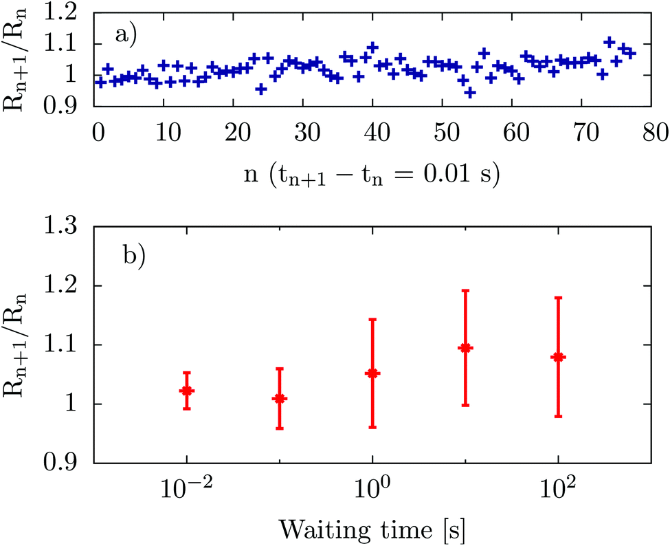 | ||
| Fig. 5 Analysis of the system stability during the waiting time Δt between two subsequent I–V measurements. (a) The ratio of the (n + 1)th and nth resistances Rn+1/Rn at Vdrive = 0 V applied during Δt = 0.01 s. (b) The average and standard deviation of Rn+1/Rn as a function of Δt. | ||
In conclusion, we studied the dynamics of the resistive switchings in Ag–Ag2S–PtIr nanojunctions. We showed that the resistance change simultaneously exhibits multiple time scales ranging from a nanosecond to seconds upon a switching voltage pulse. The resulting non-exponential transition between the OFF and ON states as well as the achievable, technologically convenient ROFF/RON = 2–10 ratios are largely affected by the amplitude and frequency of the biasing signals. This fundamental, inherent property of the Ag2S ionic conductor provides the unique opportunity for combination of GHz write/erase operations performed at bias levels of a few volts, non-volatile read-out with slower signals of a few 10 mV and robust information storage at zero bias in a two-terminal, nanometer scale analog memory device. Additionally, the observed non-exponential behaviour along with the access to tunable multiple resistance states41 open a wide range of novel applications including integrated processing and storage platforms,42 multiple bit based computation schemes43 and improved neural network modeling.44–46
This work was supported by the Hungarian Research Funds OTKA K105735 and K112918 and by the European Union 7th Framework Programme (grant no. 293797). M.C. is a grantee of the Bolyai János Research Scholarship of the HAS.
References
- J. J. Yang, D. B. Strukov and D. R. Stewart, Nat. Nanotechnol., 2013, 8, 13–24 CrossRef CAS PubMed.
- J. Borghetti, G. S. Snider, P. J. Kuekes, J. J. Yang, D. R. Stewart and R. S. Williams, Nature, 2010, 464, 873–876 CrossRef CAS PubMed.
- Y. V. Pershin and M. Di Ventra, Phys. Rev. E: Stat. Phys., Plasmas, Fluids, Relat. Interdiscip. Top., 2011, 84, 046703 CrossRef.
- A. Chung, J. Deen, J.-S. Lee and M. Meyyappan, Nanotechnology, 2010, 21, 412001 CrossRef PubMed.
- R. Waser, R. Dittmann, G. Staikov and K. Szot, Adv. Mater., 2009, 21, 2632–2663 CrossRef CAS.
- K. Terabe, T. Hasegawa, T. Nakayama and M. Aono, Nature, 2005, 433, 47–50 CrossRef CAS PubMed.
- D. B. Strukov, G. S. Snider, D. R. Stewart and R. S. Williams, Nature, 2008, 453, 80–83 CrossRef CAS PubMed.
- R. Waser and M. Aono, Nat. Mater., 2007, 6, 833–840 CrossRef CAS PubMed.
- K. Terabe, T. Hasegawa, C. Liang and M. Aono, Adv. Mater., 2007, 8, 536–542 CAS.
- Z. Wang, T. Kadohira, T. Tada and S. Watanabe, Nano Lett., 2007, 7, 2688–2692 CrossRef CAS PubMed.
- S. H. Jo and W. Lu, Nano Lett., 2008, 8, 392–397 CrossRef CAS PubMed.
- M. Aono and T. Hasegawa, IEEE Proc., 2010, 898, 2228–2236 CrossRef.
- E. Linn, R. Rosezin, C. Kugeler and R. Waser, Nat. Mater., 2010, 9, 403–406 CrossRef CAS PubMed.
- Y. V. Pershin and M. Di Ventra, Adv. Phys., 2011, 60, 145–227 CrossRef.
- I. Valov, R. Waser, J. R. Jameson and M. N. Kozicki, Nanotechnology, 2011, 22, 254003 CrossRef PubMed.
- A. C. Torrezan, J. P. Strachan, G. Medeiros-Ribeiro and R. S. Williams, Nanotechnology, 2011, 22, 485203 CrossRef PubMed.
- T. Hasegawa, K. Terabe, T. Tsuruoka and M. Aono, Adv. Mater., 2012, 24, 252–267 CrossRef CAS PubMed.
- L. Chua, IEEE Trans. Circuit Theory, 1971, 18, 507–519 CrossRef.
- T. Chang, S.-H. Jo and W. Lu, ACS Nano, 2011, 5, 7669–7676 CrossRef CAS PubMed.
- T. Ohno, T. Hasegawa, T. Tsuruoka, K. Terabe, J. K. Gimzewski and M. Aono, Nat. Mater., 2011, 10, 591–595 CrossRef CAS PubMed.
- J. J. T. Wagenaar, M. Morales-Masis and J. M. van Ruitenbeek, J. Appl. Phys., 2012, 111, 014302 CrossRef PubMed.
- D. B. Strukov and R. S. Williams, Appl. Phys. A, 2008, 94, 515–519 CrossRef PubMed.
- Z. Xu, Y. Bando, W. Wang, X. Bai and D. Golberg, ACS Nano, 2010, 4, 2515–2522 CrossRef CAS PubMed.
- A. Nayak, T. Tamura, T. Tsuruoka, K. Terabe, S. Hosaka, T. Hasegawa and M. Aono, J. Phys. Chem. Lett., 2010, 1, 604–608 CrossRef CAS.
- M. Morales-Masis, S. J. van der Molen, W. T. Fu, M. B. Hesselberth and J. M. van Ruitenbeek, Nanotechnology, 2009, 20, 095710 CrossRef CAS PubMed.
- M. Morales-Masis, H.-D. Wiemhöfer and J. M. van Ruitenbeek, Nanoscale, 2010, 2, 2275–2280 RSC.
- M. Morales-Masis, S. J. van der Molen, T. Hasegawa and J. M. van Ruitenbeek, Phys. Rev. B: Condens. Matter, 2011, 84, 115310 CrossRef.
- A. Nayak, T. Tsuruoka, K. Terabe, T. Hasegawa and M. Aono, Appl. Phys. Lett., 2011, 98, 233501 CrossRef PubMed.
- S. Menzel, U. Böttger and R. Waser, J. Appl. Phys., 2012, 111, 014501 CrossRef PubMed.
- I. Valov, I. Sapezanskaia, A. Nayak, T. Tsuruoka, T. Bredow, T. Hasegawa, G. Staikov, M. Aono and R. Waser, Nat. Mater., 2012, 11, 530–535 CrossRef CAS PubMed.
- Y. Yang, P. Gao, S. Gaba, T. Chang, X. Pan and W. Lu, Nat. Commun., 2012, 3, 732 CrossRef PubMed.
- Q. Liu, J. Sun, H. Lv, S. Long, K. Yin, N. Wan, Y. Li, L. Sun and M. Liu, Adv. Mater., 2012, 24, 1844–1849 CrossRef CAS PubMed.
- S. Menzel, S. Tappertzhofen, R. Waser and I. Valov, Phys. Chem. Chem. Phys., 2013, 15, 6945–6952 RSC.
- Y. Yang and W. Lu, Nanoscale, 2013, 5, 10076–10092 RSC.
- A. Geresdi, M. Csontos, A. Gubicza, A. Halbritter and G. Mihály, Nanoscale, 2014, 6, 2613 RSC.
- D. C. Rubin, S. Hinton and A. Wenzel, J. Exp. Psychol: Learn., Mem. Cognit., 1999, 25, 1161–1176 CrossRef.
- S. H. Jo, T. Chang, I. Ebong, B. B. Bhadviya, P. Mazumder and W. Lu, Nano Lett., 2010, 10, 1297–1301 CrossRef CAS PubMed.
- D. Kuzum, R. G. D. Jeyasingh, B. Lee and H.-S. P. Wong, Nano Lett., 2012, 12, 2179–2186 CrossRef CAS PubMed.
- R. Yang, K. Terabe, Y. Yao, T. Tsuruoka, T. Hasegawa, J. K. Gimzewski and M. Aono, Nanotechnology, 2013, 24, 384003 CrossRef PubMed.
- A. Geresdi, A. Halbritter, E. Szilágyi and G. Mihály, MRS Proc., 2011, 1331 Search PubMed.
- C. Schirm, M. Matt, F. Pauly, J. C. Cuevas, P. Nielaba and E. Scheer, Nat. Nanotechnol., 2013, 8, 645 CrossRef CAS PubMed.
- M. Di Ventra and Y. V. Pershin, Nat. Phys., 2013, 9, 200–202 CrossRef CAS.
- X. Zhao and H. Long, IEEE Trans. Evol. Comput., 2005, 3, 1996–2001 Search PubMed.
- K. K. Likharev, Sci. Adv. Mater., 2011, 3, 322–331 CrossRef CAS PubMed.
- D. Kuzum, S. Yu and H.-S. P. Wong, Nanotechnology, 2013, 24, 382001 CrossRef PubMed.
- A. Thomas, J. Phys. D: Appl. Phys., 2013, 46, 093001 CrossRef CAS.
| This journal is © The Royal Society of Chemistry 2015 |