
 Open Access Article
 This Open Access Article is licensed under a
 Creative Commons Attribution 3.0 Unported Licence
Aligned silicon nanofins via the directed self-assembly of PS-b-P4VP block copolymer and metal oxide enhanced pattern transfer†
Cian
Cummins
*a,
Anushka
Gangnaik
b,
Roisin A.
Kelly
b,
Dipu
Borah
ac,
John
O'Connell
b,
Nikolay
Petkov
b,
Yordan M.
Georgiev
b,
Justin D.
Holmes
bc and
Michael A.
Morris
*ac
aMaterials Research Group, Department of Chemistry and Tyndall National Institute, University College Cork, Cork, Ireland. E-mail: cian.a.cummins@gmail.com; m.morris@ucc.ie
bMaterials Chemistry and Analysis Group, Department of Chemistry and Tyndall National Institute, University College Cork, Cork, Ireland
cCentre for Research on Adaptive Nanostructures and Nanodevices (CRANN/AMBER), Trinity College Dublin, Dublin, Ireland
First published on 16th March 2015
Abstract
‘Directing’ block copolymer (BCP) patterns is a possible option for future semiconductor device patterning, but pattern transfer of BCP masks is somewhat hindered by the inherently low etch contrast between blocks. Here, we demonstrate a ‘fab’ friendly methodology for forming well-registered and aligned silicon (Si) nanofins following pattern transfer of robust metal oxide nanowire masks through the directed self-assembly (DSA) of BCPs. A cylindrical forming poly(styrene)-block-poly(4-vinyl-pyridine) (PS-b-P4VP) BCP was employed producing ‘fingerprint’ line patterns over macroscopic areas following solvent vapor annealing treatment. The directed assembly of PS-b-P4VP line patterns was enabled by electron-beam lithographically defined hydrogen silsequioxane (HSQ) gratings. We developed metal oxide nanowire features using PS-b-P4VP structures which facilitated high quality pattern transfer to the underlying Si substrate. This work highlights the precision at which long range ordered ∼10 nm Si nanofin features with 32 nm pitch can be defined using a cylindrical BCP system for nanolithography application. The results show promise for future nanocircuitry fabrication to access sub-16 nm critical dimensions using cylindrical systems as surface interfaces are easier to tailor than lamellar systems. Additionally, the work helps to demonstrate the extension of these methods to a ‘high χ’ BCP beyond the size limitations of the more well-studied PS-b-poly(methyl methylacrylate) (PS-b-PMMA) system.
Introduction
Resolution enhancement techniques may be required to augment current lithography tools for fabricating fine patterns to achieve more densely packed electronic devices, i.e. Moore's Law.1 Physical limits will be reached that established photolithography is unable to surpass and defining sub-wavelength dimensions/features has seen a plethora of alternative techniques explored.2 Proposed alternative lithographic patterning techniques (e.g. extreme ultraviolet lithography or multi-source electron-beam lithography) are struggling to meet required industrial criteria because of the prohibitive costs involved, an inability to achieve density multiplication and the low throughput associated limiting their overall industrial implementation.3 The use of conventional ‘top-down’ lithography to guide ‘bottom-up’ self-assembling materials i.e., directed self-assembly (DSA), is viewed as a possible compatible methodology.4 DSA of BCPs has been highlighted to define intricate future electronic circuitry enabling higher speed and reduced energy consumption per device function.5,6 The DSA of BCPs is achieved through chemoepitaxy and graphoepitaxy.7–14 Chemoepitaxy utilizes lithographic methods to define a chemical pre-pattern to regulate polymer interactions and force strict pattern alignment and order. Likewise, graphoepitaxy uses top-down optical or electron-beam techniques to topographically pattern substrates forming trenches to guide the self-assembly of BCP materials.These DSA methods are advanced for the PS-b-PMMA BCP system.7–10,14 However, PS-b-PMMA BCP is limited in the feature size attainable by having a relatively small Flory–Huggins interaction parameter (χ, measures the chemical dissimilarity of the BCP constituent blocks) of 0.04.15 For sub-15 nm BCP defined pitch sizes, the product χN (where N is the degree of polymerization) needs to be tailored so that ordered microphase separation occurs at low BCP molecular weights. High χ materials can also enable reduced line edge roughness since the interfacial width of the nanodomains are proportional to χ−0.5.16 A number of newly synthesized high χ BCPs including N-maltoheptaosyl-3-acetamido-1-propyne-block-4-polytrimethylsilylmethacrylate (MH-b-PTMSS),17 PS-b-PTMSS,18 PS-block-poly(methyltrimethylsilylmethacrylate) (PS-b-PTMSM),18 PTMSS-block-poly(D,L)lactide (PTMSS-b-PLA, χ = 0.4),19 and poly(cyclohexylethylene)-block-PMMA (PCHE-b-PMMA)20 have been developed for ultra-small features sizes as well as enhanced block contrast for etch processing. These systems extend the work on PS-block-polydimethylsiloxane (PS-b-PDMS, χ = 0.26) which combines both high χ and the presence of a Si backbone that enhances etch contrast and facile pattern transfer when used as an on-chip etch mask.21,22 Other notable commercially available high χ BCP materials for etch mask applications include poly-2-vinylpyridine (P2VP)-b-PDMS (χ ∼ 1.06),23 PS-b-P2VP (χ ∼ 0.18)24 and PS-b-PLA (χ ∼ 0.23).25–27 However to date, successful pattern transfer for high χ BCPs (other than PS-b-PDMS)22,28 has been limited. PS-b-PVP BCPs may be particularly attractive for nanolithography due to their high χ and a reactive PVP group that can enable inclusion of etch contrast agents. For example, Buriak and coworkers have shown the formation of various metallic nanowires with PS-b-P2VP block copolymers.29,30 Gu et al.24 recently illustrated fine tuning of etch chemistry and pattern transfer methodologies using cryo inductively coupled plasma etching of PS-b-P2VP BCPs.
Here, large scale coverage of highly oriented and aligned parallel cylinders via DSA and solvent vapor annealing (SVA) is demonstrated with a ‘high χ’ PS-b-P4VP system. We have used topographical patterns of hydrogen silsequioxane (HSQ) created by electron beam lithography and an asymmetric PS-b-P4VP (24![[thin space (1/6-em)]](https://www.rsc.org/images/entities/char_2009.gif) 000 kg mol−1–9500 kg mol−1) BCP self-assembly to fabricate aligned Si nanofins using etch enhanced pattern transfer. Orientation of BCP films was controlled through solvent vapor annealing (SVA) methodology forming in-plane cylinders (i.e. horizontal to the substrate surface, C‖). PS-b-P4VP templates were developed through a surface reconstruction strategy and etch contrast was enhanced via incorporation of metal oxide material either iron oxide (Fe3O4) or aluminium oxide (γ-Al2O3). The metal oxide inclusion enabled an effective pattern transfer producing uniform arrays of Si nanofins over macroscopic areas as characterized by scanning electron microscopy (SEM) and transmission electron microscopy (TEM). Whilst line-space features of PS-b-P4VP systems have been shown previously,31,32 we further demonstrate the mask etch application potential of PS-b-P4VP by integrating DSA and metal oxide hardmask inclusion for high aspect ratio (1:4) Si pattern transfer. Critically, previous work only details orientation control (i.e. vertical or parallel to the surface plane). However, we show pattern alignment (to a surface direction) of the arrangements which is critical for application. This also means that we are essentially producing defect-free patterns over large areas. The methodology described herein resulted in highly parallel nanofin structures with translational alignment and registration of ∼10 nm feature sizes within HSQ gratings.
000 kg mol−1–9500 kg mol−1) BCP self-assembly to fabricate aligned Si nanofins using etch enhanced pattern transfer. Orientation of BCP films was controlled through solvent vapor annealing (SVA) methodology forming in-plane cylinders (i.e. horizontal to the substrate surface, C‖). PS-b-P4VP templates were developed through a surface reconstruction strategy and etch contrast was enhanced via incorporation of metal oxide material either iron oxide (Fe3O4) or aluminium oxide (γ-Al2O3). The metal oxide inclusion enabled an effective pattern transfer producing uniform arrays of Si nanofins over macroscopic areas as characterized by scanning electron microscopy (SEM) and transmission electron microscopy (TEM). Whilst line-space features of PS-b-P4VP systems have been shown previously,31,32 we further demonstrate the mask etch application potential of PS-b-P4VP by integrating DSA and metal oxide hardmask inclusion for high aspect ratio (1:4) Si pattern transfer. Critically, previous work only details orientation control (i.e. vertical or parallel to the surface plane). However, we show pattern alignment (to a surface direction) of the arrangements which is critical for application. This also means that we are essentially producing defect-free patterns over large areas. The methodology described herein resulted in highly parallel nanofin structures with translational alignment and registration of ∼10 nm feature sizes within HSQ gratings.
Results and discussion
Scheme 1 shows the overall process flow for the fabrication of Si nanofins following the DSA of PS-b-P4VP block copolymer in HSQ trenches. Large areas of translationally ordered, in plane (C‖) P4VP were generated by confinement in the HSQ topography. Experimentally robust processes were established for developing P4VP C‖ patterns and their subsequent impregnation with Fe3O4 and γ-Al2O3 hardmask materials and eventual substrate pattern transfer. PS-b-P4VP thin films were spin coated onto HSQ topographically patterned substrates (such that HSQ feature spacing was 32n nm where n is an integer and 0 < n < 8). Full SEM characterization of these substrates is shown in ESI Fig. S1.† SVA was carried out in an ambient atmosphere of chloroform and pattern transfer was then optimized for the DSA defined features.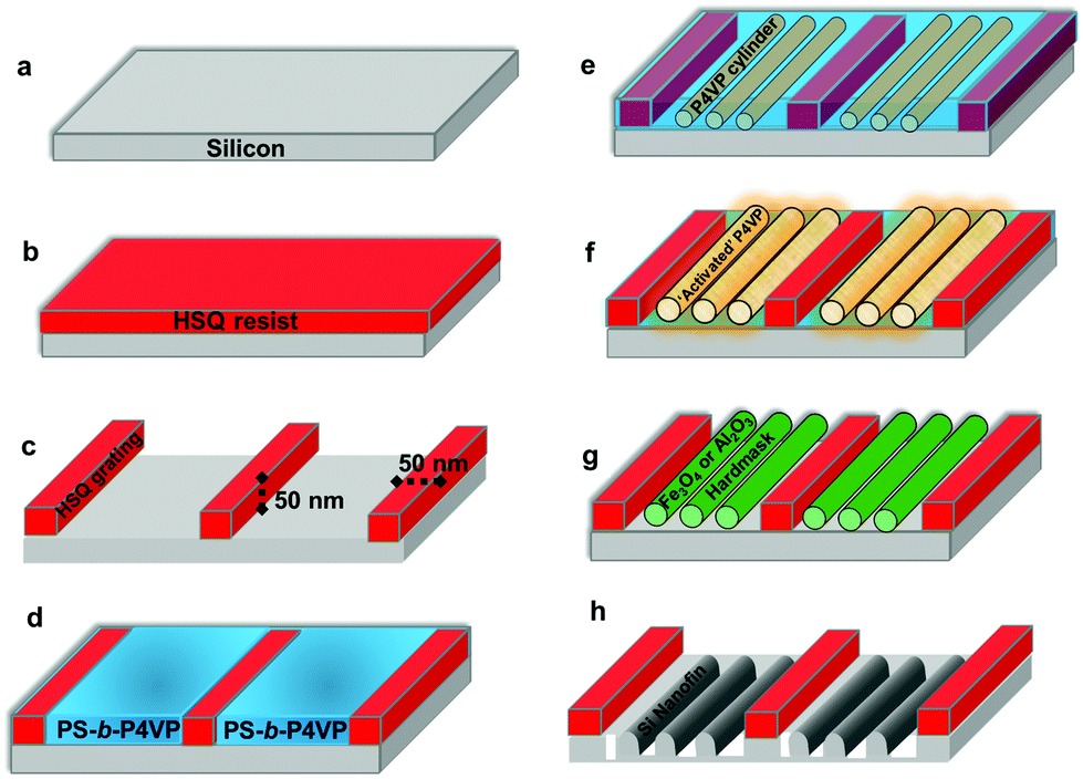 | ||
| Scheme 1 Overall process flow enabling Si nanofins via an enhanced metal oxide pattern transfer. (a) Si substrate (b) uniform HSQ resist material spin coated (c) electron beam lithography used to define 50 nm HSQ gratings at different pitches (see experimental) (d) PS-b-P4VP BCP spin coated (e) solvent vapor annealing of BCP film in chloroform vapors at room temperature producing P4VP cylinders in plane (f) film exposed to ethanol vapors to form ‘activated’ porous P4VP nanodomains (g) iron or aluminium oxide formed via inclusion and UV/ozone treatment (h) pattern transfer to underlying Si forming aligned Si nanofins. | ||
The graphoepitaxial alignment of PS-b-P4VP within the topographical HSQ substrates was carefully optimized using film thickness and SVA conditions. 0.5, 1 and 2 wt% PS-b-P4VP BCP solutions were spin coated onto Si substrates that had been ultrasonically cleaned. Characterization of 1 and 2 wt% films were initially examined after a 3 hour SVA period and data are presented in ESI Fig. S2–S9.† The influence of different surface chemistries were also examined for the 0.5 wt% films (see ESI Fig. S10–S16†). Films thicknesses were measured after SVA for 2 hours at 52.6 and 97.2 (±0.15) nm for 1 and 2 wt% films respectively. A color change associated with increased swelling33 was observed for these films but not the thinner films as described below (Fig. 1). Relief structures such as ‘islands’ and ‘holes’ were observed in these thicker films and visible in both optical and atomic force microscopy (AFM). The thicker films proved unsuitable for nanolithography due to irregular thickness and also that they contained more than one layer of parallel cylinders. In comparison, an optical image (Fig. S13b†) of the 0.5 wt% film showed film thickness uniformity and the thickness of the film at 24.4 (±0.15) nm is consistent with a single layer of cylinders (as proven in TEM data presented below). Although 24.4 nm is below the ideal commensurability of the system (since the cylinder centre to centre spacing is 32 nm) it is suggested that under the chloroform solvent vapor that the thickness approaches an ideal value.
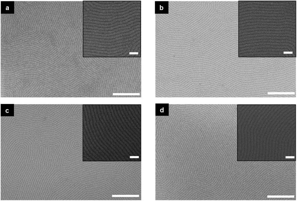 | ||
| Fig. 1 PS-b-P4VP BCP films were spin coated from a 0.5 wt% solution on to acetone degreased Si substrates. Top-down SEM images are shown in (a)–(d) after solvent vapor annealing with chloroform at room temperature (∼290 K) of a 24 nm thick PS-b-P4VP BCP film for (a) 30 minutes, (b) 1 hour, (c) 2 hour and (d) 3 hours respectively. Note films were exposed to ethanol vapors following solvent vapor annealing to create porous structures. Scale bars are 500 nm, while inset scale bars are 100 nm. | ||
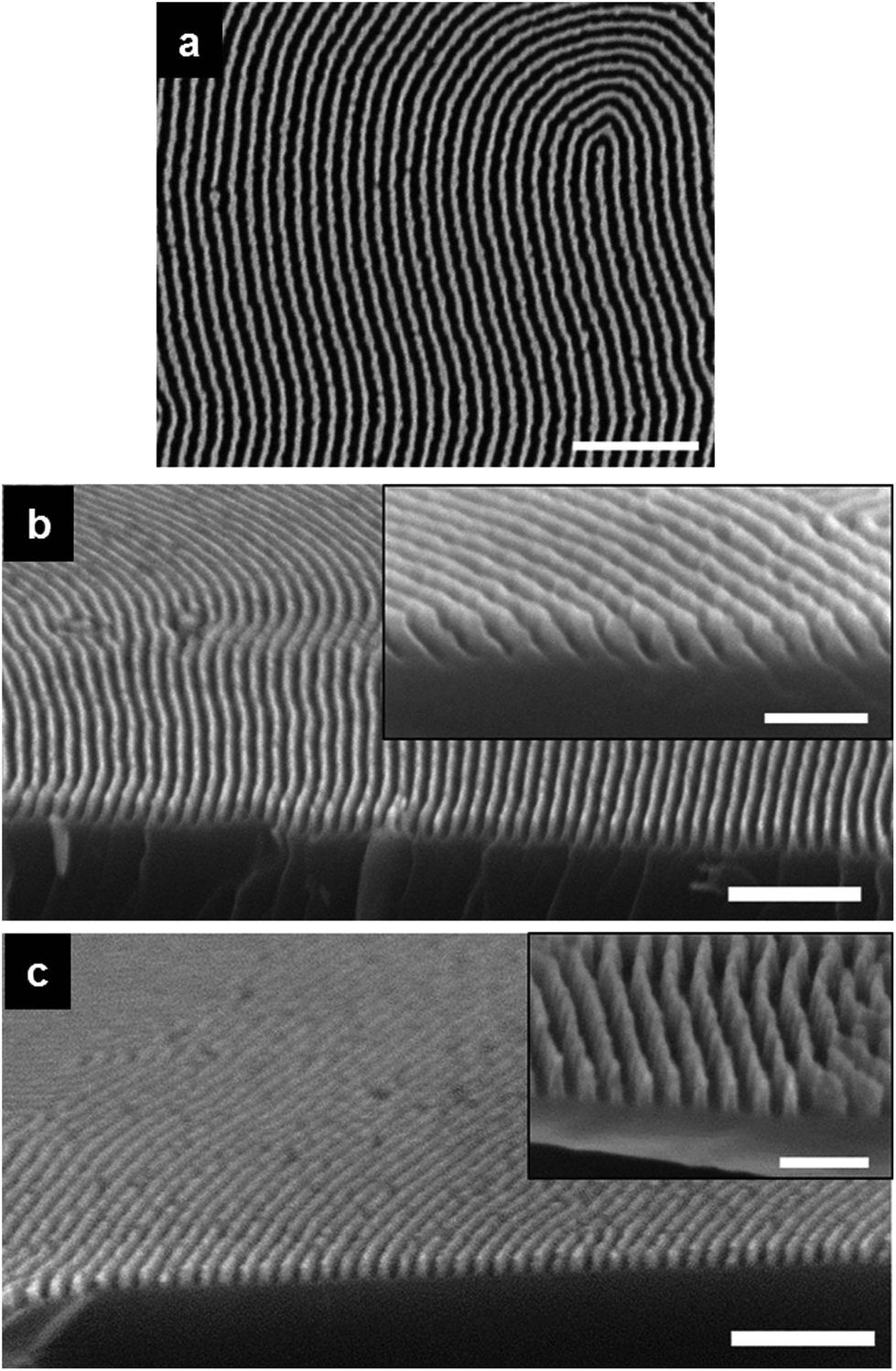
Thus, the solvent annealing conditions of the 0.5 wt% films was examined in detail. Fig. 1a–d show SEM characterization of the line pattern evolution for 0.5 wt% films with chloroform at room temperature (∼290 K) from 30 minutes up to 3 hours (note films were selectively swelled using ethanol vapor to provide SEM contrast). The initial spin cast 0.5 wt% film (AFM image, Fig. S13c†) showed poorly ordered P4VP cylinders normal (C⊥) to the substrate. The top-down SEM images in Fig. 1 show the film surface after 30 minutes to 3 hours. Well-developed line (C‖) patterns were observed with defects reducing as the anneal period was increased. The average domain feature size and cylinder periodicity (Co) for the films was 20 nm and 32 nm respectively for all samples. Self-assembled patterns were developed in HSQ trenches as shown in ESI Fig. S17.† Patterns were stained using ruthenium tetroxide vapor to enhance contrast. In situ ellipsometry suggests the swollen thickness does not reach the theoretically ideal thickness of 32 nm and after 2 hours SVA the measured thickness was 26.1 nm (see Fig. S18a and b†). It should be noted that we have observed that the ideal cylinder structure is compressed in thin films and this somewhat lower value might represent the true ideal thickness.34 The relatively small increase in film thickness (∼15%) under SVA is probably due to the limited swelling of the BCP film during annealing as chloroform is a nonselective solvent for pure PS-b-P4VP.33 Solubility parameters for chloroform, PS and P4VP are 19.0, 18.6 and ∼23 MPa1/2 respectively.32,35 The use of chloroform did result in formation of P4VP C‖ while PS selective annealing solvents (e.g. tetrahydrofuran or 1,4 dioxane) gave P4VP C⊥ arrangements. It should be noted that the SVA conditions and process window was optimized for this particular PS-b-P4VP system and cannot be considered universally applicable for all PS-b-P4VP BCP systems.36 Following SVA in chloroform we believe we have formed cylindrical morphological structures but we cannot definitively rule out other phases without through film analysis (GISAXS or cross-section TEM). However, we do believe that the lack of swelling with chloroform may ensure minimal change in the effective volume composition of the BCP film and thus the likely formation of cylinder structures. Substrates without any surface modification (acetone only cleaned Si or bare Si) gave the best ordered line patterns and thus this window was used for BCP deposition on planar and HSQ substrates. Acetone only cleaned substrates were used as degreasing the substrates provided a uniform film.
Surface reconstruction is a popular method for creating ‘nanoporous’ structures after SVA for asymmetric PS-b-P4VP37,38 and as shown in Fig. 1, it is sufficient to generate SEM contrast. However, the ethanol reconstruction process needed to be carefully controlled and destruction of the film morphology was observed when the SVA films were immersed in ethanol (see Fig. S19b and c†) for extended periods. 10 minutes immersing times did produce porous structures (Fig. S19a†) of reasonable quality but at longer times significant distortion of the PS matrix occurs through swelling of the P4VP nanodomains. To create the nanoporous structure without distortion, we used a similar approach to Gowd et al.39 where the film was exposed to ethanol vapor for 20 minutes. We believe that this allows more limited swelling of the P4VP and prevents degradation of the P4VP line patterns. As shown in previous work it is unlikely that this results in a fully developed pore system.40 This differs from the ethanol treatment used for cylinder forming PS-b-PEO BCP systems where the pore system is well developed and suggests effective etching of the PEO.41,42 The nature of these activation techniques is under debate but it is clear that well-defined inclusion formed patterns are reliant on the optimization of the activation process. Fig. 2a–d shows top-down SEM images of highly aligned porous features of PS-b-P4VP films in HSQ gratings with 160, 192, 224 and 265 nm channel width dimensions. The methodology developed for planar films can be extended to the HSQ topographical substrates as shown in Fig. 2. Notably, the influence of the HSQ gratings is evident from Fig. 2c and d as one can see the ‘fingerprint’ pattern in the open area aligned in the HSQ guiding features over large areas.
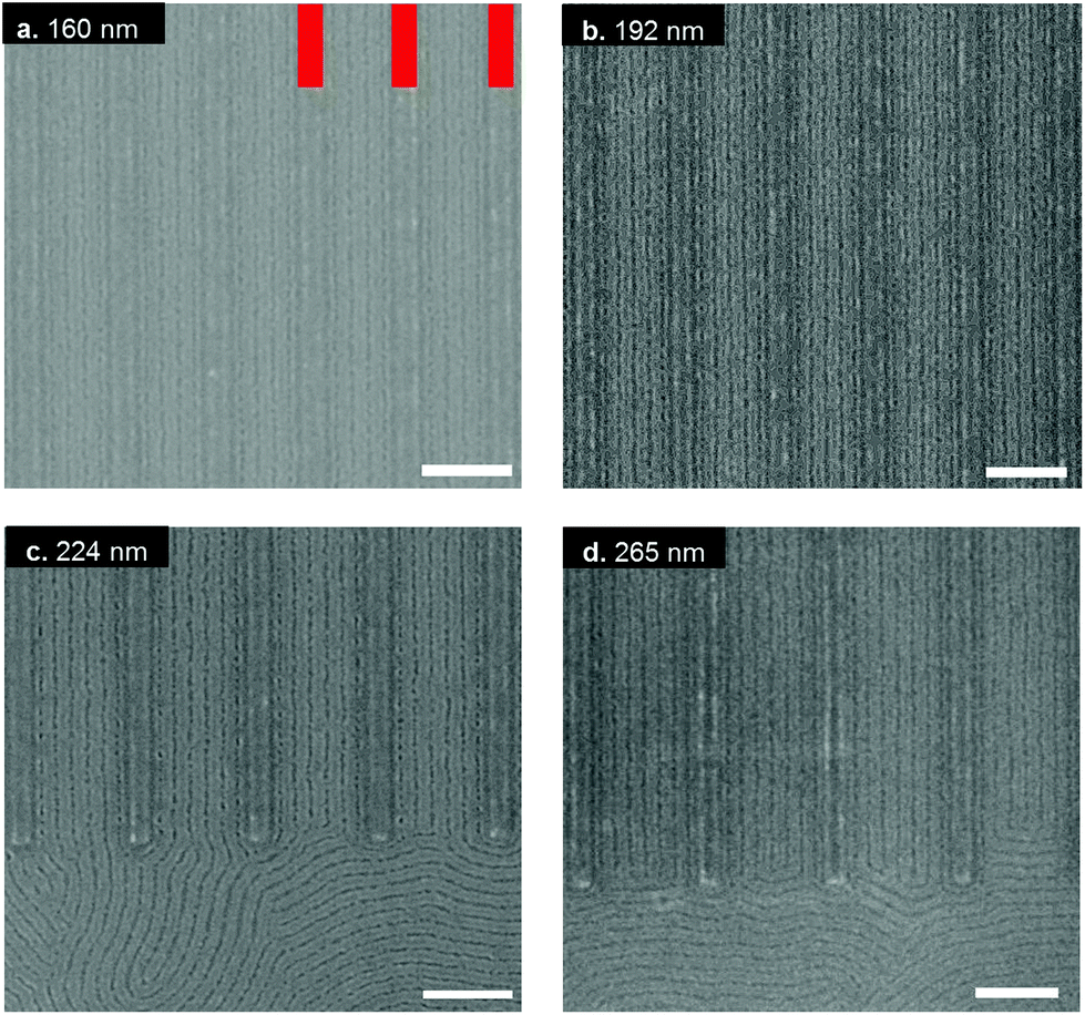 | ||
| Fig. 2 Top-down SEM images of graphoepitaxially aligned porous PS-b-P4VP templates in HSQ gratings following swelling of P4VP domains using ethanol vapor. (a)–(d) Show alignment of PS-b-P4VP features in 50 nm HSQ gratings (red bars in image a) at channel widths of (a) 160 nm, (b) 192 nm, (c) 224 nm and (d) 265 nm. (c) and (d) Show areas where alignment has taken place from open areas in to the HSQ trench gratings. Scale bars are 200 nm. | ||
Following surface reconstruction, the ‘activated’ PS-b-P4VP acts as a template for the development of metal oxide nanowires to form a hardmask for the pattern transfer process. Employing Fe3O4 is an attractive and facile route to act as an etch mask during plasma etching due to the robust nature of the oxide material which allows the development of high fidelity nanostructures.40–42 Improving etch contrast between polymer blocks is extremely important for pattern transfer and innovative methods have been explored. For example, Elam, Darling and co-workers have developed a process involving atomic layer deposition coined sequential infiltration synthesis (SIS) to enhance the etch contrast of as formed PS-b-PMMA BCP patterns with inorganic material.43,44 Exotic BCPs containing an inorganic block have been reviewed lately showing potential for lithographic purposes.45 Here we use simple metal nitrate salts to provide a robust inorganic moiety giving high etch contrast. The metal nitrate (iron or aluminium) solution was spin coated on the nanoporous polymer film structure and the surrounding polymer template was then removed via UV/O3 treatment. Fig. 3a displays large scale coverage of the Fe3O4 nanowires and the TEM inset shows a slightly elliptical structure that may reflect the elliptical form of the cylinders noted before.34 The inset also shows that what may be a small amount of Fe3O4 material resides across the polymer substrate interface. This might result from a thin PVP wetting layer (as P4VP has a higher affinity to the hydrophilic native oxide layer)33 in the self-assembled PS-b-P4VP structure. This was not problematic for pattern transfer and this suggests these darker areas may instead result from electron beam scattering events at the interface. Further characterization from the STEM images in Fig. 3b show both low resolution and high resolution (inset) Fe3O4 nanowires with high and regular uniformity. The EDX included in Fig. 3b reveals the presence of iron in the expected regions40 (but not in areas between wires suggesting that a scattering process is responsible for the apparent thin film between wires) as well as Si (from the substrate) and oxygen (from the Si oxide layer and from the Fe3O4). γ-Al2O3 inclusion was also carried out and the SEM image in Fig. 3c show well-defined uniform nanowires. γ-Al2O3 nanowires were produced in a similar manner to Fe3O4 inclusion with an ethanolic metal precursor and the high uniformity is comparable to the Fe3O4 nanowires described above. Fig. 4a shows a large open area of HSQ topographical substrate with well-defined γ-Al2O3 nanowires. Fig. 4b–g displays the DSA of HSQ line gratings with aligned γ-Al2O3 nanowire features over large areas with channel widths of 96 nm, 128 nm, 160 nm, 192 nm, 224 nm and 265 nm respectively. Distinct γ-Al2O3 nanowires features are observed in all images with two γ-Al2O3 nanowire features seen in the HSQ gratings with channel width of 96 nm and a total of seven γ-Al2O3 nanowire features demonstrated in the 265 nm channel width. The γ-Al2O3 nanowires mimic the nanoporous template used and possess centre to centre spacings (32 nm) comparable to the original PS-b-P4VP BCP film. Fe3O4 inclusion in a 265 nm channel width HSQ grating is also shown over large areas in ESI Fig. S20.†
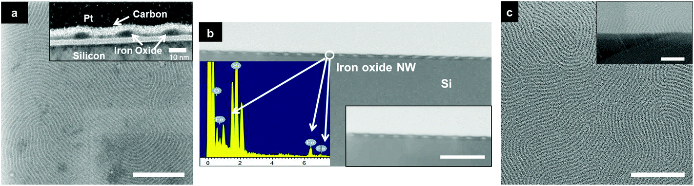 | ||
| Fig. 3 (a) Top-down SEM image of Fe3O4 nanowire array after UV/O3 treatment. Inset in (a) shows cross section TEM of Fe3O4 nanowires/substrate interface. (b) EDX spectrum of Fe3O4 nanowire array and HAADF image and inset show uniformity and regularity of Fe3O4 nanowire array. (c) Top-down SEM image of γ-Al2O3 nanowire arrays after UV/O3 treatment. Inset in (c) shows cross-section SEM view of γ-Al2O3 nanowires. Scale bars are 500 nm in (a) and (c) and represent 100 nm in (b). | ||
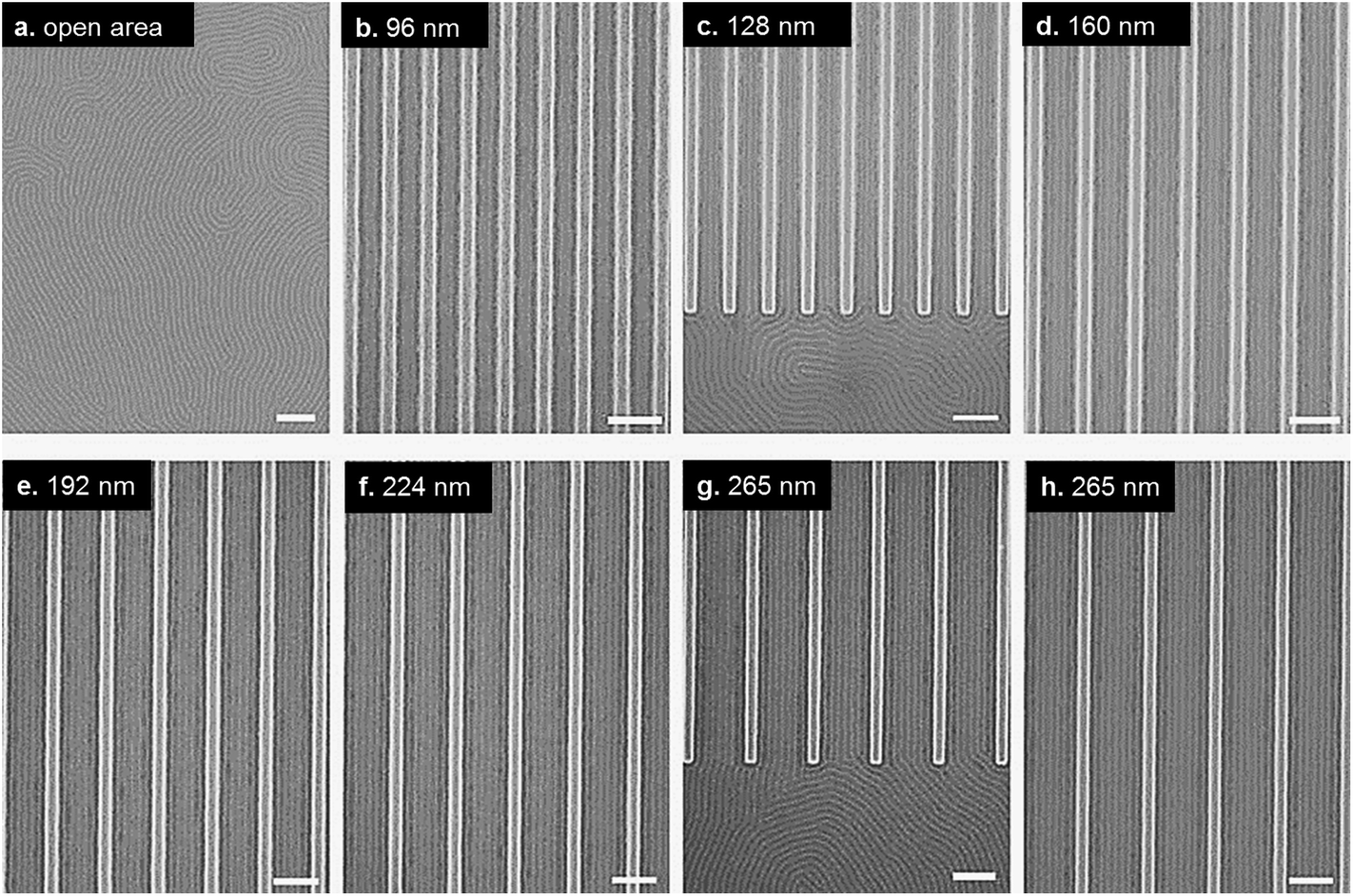 | ||
| Fig. 4 (a) Shows top-down SEM image of γ-Al2O3 nanowires in open area of HSQ substrate. (b)–(h) Top-down SEM images of aligned γ-Al2O3 nanowires in 50 nm HSQ gratings with channel widths indicated in image. All scale bars are 200 nm. | ||
X-ray photoelectron spectroscopy (XPS) was used to elucidate the chemical composition of the metal nanowire structures developed from metal nitrate ethanolic solutions. Fig. 5a and b show the high resolution spectra of Fe 2p and Al 2p core level binding energies of Fe3O4 and γ-Al2O3 nanowires formed following UV/ozone treatment for 3 hours. The ozonation process allowed complete or near-complete removal (as determined by C 1s signal reduction) of polymer material to form Fe3O4 nanowires (as shown in Fig. 3a and b) and γ-Al2O3 nanowires (Fig. 3c). The survey and high resolution O 1s spectra for the Fe3O4 nanowires can be found in ESI Fig. S21.† The metal 2p features were processed with the CasaXPS software using a Shirley background subtraction and curve-fitting with Voigt profiles. For the Fe 2p core level, peaks are found at 713.5 eV (Fe 2p3/2) and 724.9 eV (Fe 2p1/2) respectively. The values match previously reported literature values.40,42 The 2p3/2:2p1/2 ratio was the expected value of 2:1. Fig. 5b displays XPS of the Al 2p core level binding energy corresponding to the nanowire sample shown in Fig. 3c. The Al 2p core level binding energy (Fig. 5b) shows the characteristic peak for Al 2p at 73.9 eV typical of γ-Al2O3 and this was consistent with the O 1s spectra (ESI Fig. S22†).46
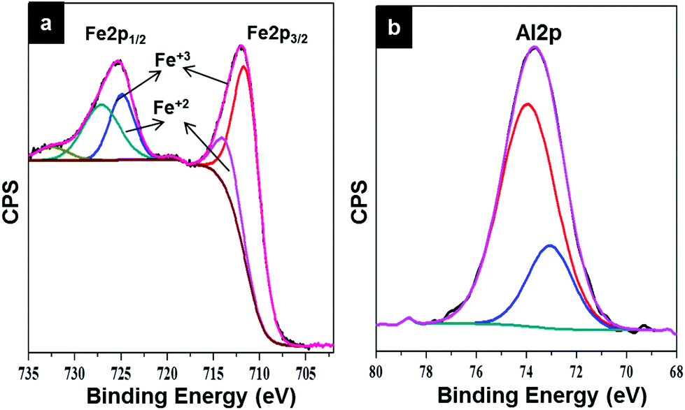 | ||
| Fig. 5 (a) High resolution XPS spectra of Fe 2p core level of iron oxide (Fe3O4) nanowires following UV/O3 treatment. (b) High resolution XPS spectra of Al 2p core level of aluminium oxide nanowires (γ-Al2O3) following UV/O3 treatment. Survey spectra and high resolution O 1s core level spectra are shown in ESI Fig. 21 and 22† for both samples. | ||
It has been speculated that the pattern transfer of an on-chip etch mask is second only to lithography in importance.47 All etch processes are challenging24 and it is vital that pattern transfer methods are highly selective47,48 so that DSA of BCPs can move successfully from ‘lab to fab’. These Fe3O4 and γ-Al2O3 nanowires can act as efficient hardmasks for pattern transfer. C4F8–H2 was employed to etch the native oxide layer thus exposing the underlying Si which was then subject to a Si etch (C4F8–SF6). The top-down SEM image in Fig. 6a are of the Si nanofins following pattern transfer of the Fe3O4 nanowires using a short Si oxide etch (5 seconds) and an ICP Si etch (1 minute 30 seconds). Note that the rough edges of the hardmask from the top-down SEM image in Fig. 6a are due to the Fe3O4 nanowire material that will inevitably be etched with extended plasma etching. However, the damage to the Fe3O4 hardmask is not transferred to the underlying Si material (see Fig. 6b, c and 7).
 | ||
| Fig. 6 (a) Top-down SEM of Si nanofins following plasma etching of Fe3O4 nanowire hardmask for 1 minute and 30 seconds. (b) Cross-section SEM image of sample (a) while (c) shows cross-section SEM image of an Fe3O4 nanowire hardmask plasma etched for 2 minutes. Insets in (b) and (c) show highly defined uniform nanofin arrays. Main scale bars are 250 nm while inset scale bars represent 100 nm. | ||
 | ||
| Fig. 7 (a) Low resolution TEM image of Si nanofin array following plasma etching Si for 1 minute and 30 seconds using Fe3O4 nanowire hardmask. (b) and (c) High resolution TEM images of Si nanofins with 10 nm feature size and 16 nm half-pitch as shown in (a). | ||
In contrast, the cross-section SEM in Fig. 6b and the inset show the regularity of the Si structures where the Si was etched for 1 minute and 30 seconds. This provides evidence for the mechanical strength of the hardmask, and while some rough edges are visible from top-down SEM (Fig. 6a) these did not affect the Si structure as seen from the TEM characterization below. As described elsewhere,40 Fe3O4 can be etched away/removed from the surface of the Si structures without damaging the existing Si. Fig. 6c shows Si nanofins after 2 minutes Si etching. The profile seen in the cross-section SEM image and inset reveal an even greater depth and definition to the Si nanofins etched for 1 minute and 30 seconds in Fig. 6b. TEM analysis was carried out on the Si nanofins fabricated from the Fe3O4 nanowire hardmask template shown in Fig. 6a and b. The corresponding TEM characterization of the Si etched for 1 minute and 30 seconds are shown in Fig. 7a–c and reveal the uniformity of the etch with dimensional control owing to the Fe3O4 nanowire hardmask. The periodicity of the Si structure pattern (Co = 32 nm) remains similar to the initial microphase separated, reconstructed template and Fe3O4 nanowire patterns. The etched Si nanostructures possess features sizes of ∼10 nm and etch depths of ∼40 nm.
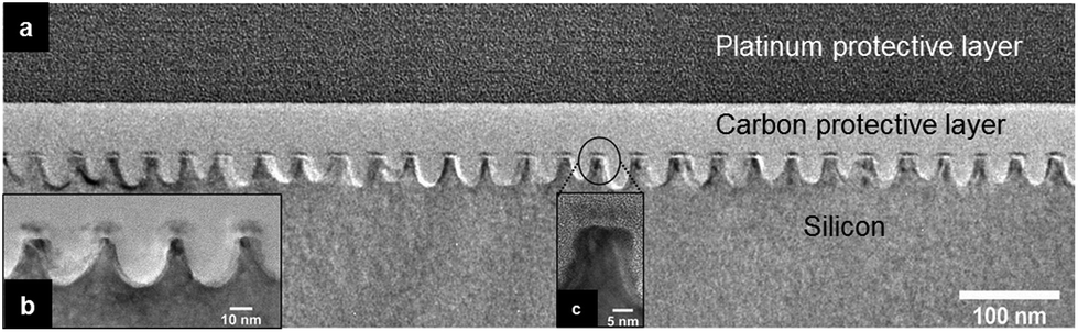
Similarly, we examined the effectiveness of the γ-Al2O3 hardmask material. The etching procedures were extended to the γ-Al2O3 hardmask showing similar results. However, it should be noted that later etches were performed without the native oxide etch. The native oxide etch can sometimes result in significant damage to the γ-Al2O3 hardmask and, thus, limits etch fidelity. Fig. 8a displays the top-down SEM image of Si nanofin structures following etching of Si for 1 minute and 30 seconds using the γ-Al2O3 hardmask. The top-down and cross-section SEM images in Fig. 8a and b reveal a highly uniform etch with homogeneity across the Si surface. The use of a different metal oxide material shows the versatility of the metal-ethanolic precursor solution as it is simple, inexpensive, provides well-defined nanowires and acts as a robust hardmask for pattern transfer. Fig. 8c shows the resulting profile from a 2 minute Si etch using the γ-Al2O3 material. The cross-section view and inset in Fig. 8c reveals a homogenous etching procedure with high reproducibility.
 | ||
| Fig. 8 (a) Top-down SEM image of pattern transfer of γ-Al2O3 hardmask nanowires on planar Si generating Si nanofins. (b) Cross-section SEM view of sample (a) after 1 minute and 30 seconds of Si etching. (c) Cross-section SEM view of Si nanofins over large area following 2 minutes of Si etching with γ-Al2O3 as hardmask. Inset in (c) reveals the vertical profile and uniform nature of the nanofins. Main scale bars are 250 nm while inset scale bars represent 100 nm. | ||
Finally we demonstrate the pattern transfer producing aligned Si nanofins generated from the γ-Al2O3 nanowire hardmask using the HSQ gratings for DSA application. Fig. 9a–c shows the top-down SEM images of Si nanofins following pattern transfer using Si etch (SF6–C4F8) for 1 minute and 30 seconds. Fig. 9a displays an open area of the HSQ substrate where the alignment of one P4VP cylinder was directed. The nanofin shows good contrast in comparison to γ-Al2O3 features shown earlier (Fig. 4) due to the Si etch. Distinct nanofins were also produced in the 160 nm and 265 nm trenches displaying 4 and 7 Si nanofins respectively as displayed in Fig. 9b and c.
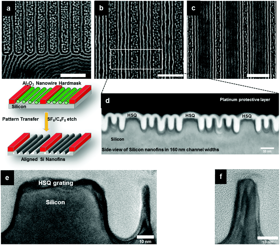 | ||
| Fig. 9 Top-down SEM images of pattern transferred Si nanofins in ∼50 nm HSQ gratings at channel widths of (a) 64 nm, (b) 160 nm and (c) 265 nm respectively. Schematic shows process for pattern transfer of aligned γ-Al2O3 nanowire hardmask. (d) Cross-section TEM of aligned Si nanofins in HSQ gratings possessing channel widths of 160 nm. (e, f) Show high resolution TEM images of Si nanofins fabricated from γ-Al2O3 nanowire hardmask. Scale bars are 250 nm unless indicated. | ||
One can also see that the feature size of the nanofins aligned next to the HSQ sidewalls in the larger trench width (265 nm) is slightly smaller and we speculate that this may be due to swelling effects during SVA or the ‘activation’ step. The issue does not affect the pattern transfer of the γ-Al2O3 nanowires in the graphoepitaxy process however we suggest that by increasing the trench widths initially this problem may be overcome, and could lead to uniform nanofin formation by accounting for excess swelling of domains during SVA. A low resolution TEM image in Fig. 9d shows the uniformity of the Si etch in the 160 nm channel width with the γ-Al2O3 material acting as an effective etch stop. Feature sizes were measured at ∼10 nm while the etch depth was ∼40 nm i.e. an aspect ratio of 1:4. The high-resolution TEM images of Si nanofins are displayed in Fig. 9e and f revealing the uniformity of the nanofin structure.
Experimental
Materials
Planar substrates used were highly polished single-crystal silicon <100> wafers (p-type) with a native oxide layer of ∼2 nm. Poly(styrene)-block-poly(4-vinylpyridine) was purchased from Polymer Source, Inc., Canada, with a molecular weight of Mn = 33.5 kg mol−1 (MnPS = 24 kg mol−1; MnP4VP = 9.5 kg mol−1, fPS = 0.70), a polydispersity (Mw/Mn) of 1.15 (where, Mn and Mw are number average and weight average molecular weights) and was used without further purification. Fe2(NO3)3·9H2O (iron(III) nitrate nonahydrate), Al(NO3)3·9H2O (aluminium nitrate nonahydrate, ACS reagent, ≥98%), acetone (ACS reagent, ≥99.5%) chloroform (for HPLC, ≥99.9%, contains 0.5–1.0% ethanol as stabilizer), Tetrahydrofuran (inhibitor-free, CHROMASOLV Plus, for HPLC, ≥99.9%), Toluene (CHROMASOLV, for HPLC, 99.9%), ethanol (dehydrated, 200 proof) were purchased from Sigma-Aldrich and used without further purification unless otherwise stated. De-ionized (DI) water was used wherever necessary.HSQ substrate preparation and substrate cleaning
Ten × 10 mm bulk silicon <100> oriented substrates, nominal resistivity 0.001 Ω cm, were used for all DSA experiments. The substrates were first patterned using a HSQ EBL (Raith e-LiNE plus) process prior to deposition of the PS-b-P4VP block copolymer (BCP). The substrates were initially degreased via ultrasonication in acetone and iso-propanol (IPA) solutions (2 × 2 min), dried in flowing N2 gas and baked for 2 minutes at 393 K in an ambient atmosphere to remove any residual IPA. The substrates were then spin coated (500 rpm, 5 seconds, 2000 rpm, 32 seconds) with a 2.4 wt% solution of HSQ (XR-1541 Dow Corning Corp.) in MIBK to produce a ∼50 nm film of HSQ. The wafer was then baked at 393 K in an ambient atmosphere for 3 minutes prior to transfer to the EBL system for exposure. Arrays of 50 nm wide lines at pitches of (32n + 50) nm were exposed, where n is an integer and 0 < n < 8. HSQ pitches were measured at ∼110, 145, 175, 205, 240, 270, and 300 nm. Following electron beam exposure the samples were developed in an aqueous solution of 0.25 M NaOH, 0.7 M NaCl for 15 seconds, followed by rinsing in flowing DI water for 60 seconds and 15 seconds rinse in IPA. The samples were then blown dry in flowing N2 gas.Block copolymer film preparation and solvent vapor anneal
0.5 weight% solutions of PS-b-P4VP BCP were prepared in toluene–THF (80:20). The solutions were left stirring overnight to ensure complete dissolution. Prior to spin coating planar Si or HSQ substrates were sonicated for 20 minutes with acetone. Following this surface cleaning, the substrates were then further rinsed in acetone and blown dry with nitrogen. Spin coating of the PS-b-P4VP BCP solution was carried out at 3200 rpm for 30 seconds. Solvent vapor annealing was carried out in the conventional manner with a small vial containing 8–10 ml of chloroform placed inside a glass jar (150 ml) with PS-b-P4VP sample for 30 minutes to 3 hours (room temperature ∼290 K). Samples were removed from the glass jars after the desired anneal time and allowed to evaporate the trapped solvent at ambient conditions. The films did not exhibit any major swelling during annealing as the films were transparent throughout (same as spin cast). Surface reconstruction was carried out by placing the solvent annealed PS-b-P4VP sample in a glass jar with ethanol vapors for 20 minutes. After this vapor treatment, the sample was removed and left to dry at room temperature. This provided enough time for swelling of the P4VP domains to enable the reconstructed template to form for subsequent deposition of the metal nitrate solutions.
Metal oxide nanowire pattern fabrication
Fe2(NO3)3·9H2O (iron nitrate hexahydrate) and Al(NO3)3·9H2O (aluminium nitrate nonahydrate, ACS reagent, ≥98%) solutions of 0.4 wt% were prepared in ethanol and spin-coated on to the ethanol reconstructed samples for 30 seconds at 3200 rpm. UV/O3 treatment was used to oxidize the precursor and remove polymer. Samples were UV/O3 treated for 3 hours in a UV/ozone system (PSD Pro Series Digital UV Ozone System; Novascan Technologies, Inc., USA). The UV source is two low pressure mercury vapor grid lamps. Both lamps have an output current of 0.8–0.95 A and power of 65–100 W, as reported by the manufacturer, and have strong emissions at both wavelengths of UV radiation (184.9 nm and 253.7 nm). The system produces highly reactive ozone gas from oxygen that is present within the chamber.Pattern transfer recipes
An STS, Advanced Oxide Etch (AOE) ICP etcher was used for etching to pattern transfer the iron oxide and aluminium oxide nanowires to the underlying Si substrate. The general plasma etch methodology for pattern transfer was as follows; the initial etch was to remove the native oxide and then Si etch time was varied to form fins with different heights. The native oxide layer etch was carried out for 5 seconds using a combination of C4F8–H2 gas mixture (21 sccm/30 sccm) using an ICP coil power of 800 W and a Reactive Ion Etching (RIE) power of 80 W. Following this, nanofin fabrication involved a controlled gas mixture of C4F8–SF6 at flow rates of 90 sccm/30 sccm respectively and the ICP and RIE power were set to 600 W and 15 W respectively at a chamber pressure of 15 mTorr. Note that further details on the above etches can be found in previously reported work by Ghoshal et al.41,42 Also as mentioned above, Fe3O4 can be removed via wet etch procedures (oxalic acid), note that the γ-Al2O3 hardmask used here can be removed using a mild base (NaOH) treatment.Characterization
PS-b-P4VP BCP film thicknesses were measured with a spectroscopic ellipsometer “J. A. Woollam Ellipsometer” at a fixed angle of incidence of 70°, on at least three different places on the sample and was averaged as the film thickness. A two layer model (SiO2 + BCP) for total BCP film was used to simulate experimental data. Atomic Force Microscopy (AFM) (Park systems, XE-100) was operated in AC (tapping) mode under ambient conditions using silicon microcantilever probe tips with a force constant of 42 N m−1. Topographic and phase images were recorded simultaneously. Scanning Electron Microscopy (SEM) images were obtained by a FEI Helios Nanolab 600i system at an accelerating voltage of 5 kV and at a working distance of 4 mm. For cross-section SEM images, the substrate was cleaved in half and positioned perpendicular to the incident beam of electrons. The stage was then tilted at an angle of 20°. Transmission Electron Microscopy (TEM) lamella specimen were prepared using the Helios NanoLab DB FIB and were analysed by JEOL 2100 high resolution transmission electron microscope operating at an accelerating voltage of 200 kV. Domain size, periodicity of HSQ trenches and feature sizes etc. were measured from SEM and TEM data using ImageJ software. X-ray Photoelectron Spectroscopy (XPS) was performed on Vacuum Science Workshop CLASS100 high performance hemispherical analyser using Al Kα (hv = 1486.6 eV) X-ray at 200 W power. Spectra were obtained at a take-off angle of 90°. Photoemission peak positions were corrected to C 1s at a binding energy of 284.8 eV.Conclusions
In summary, a straight forward, low cost and industrial compatible methodology for the fabrication of sub-wavelength semiconductor features has been demonstrated. SVA was shown to be an extremely effective route for controlling and optimizing cylindrical morphology in an asymmetric PS-b-P4VP BCP system. Furthermore, the ability to develop and control the orientation of the cylindrical morphology is promising for line space features for on-chip etch mask application. The tuning of the film thickness of the PS-b-P4VP is a significant process step for forming a monolayer of cylinders in thin film for etch mask application. Creating an ultrathin mask is important for the subsequent pattern transfer to the device active layer that the mask patterns. The TEM characterization presented in this work shows the ability of PS-b-P4VP to form well oriented C‖ that enable metal oxide inclusion. Additionally, enhancing etch contrast over large areas via metal oxide inclusion technique was shown allowing a facile pattern transfer. The pattern transfer of the on-chip etch mask was shown to be extremely successful for both the Fe3O4 and γ-Al2O3 hardmask material on planar Si. Si nanofins were shown to be uniform from TEM characterization with feature sizes of sub-12 nm. DSA of the PS-b-P4VP line patterns via a graphoepitaxial approach was also demonstrated employing HSQ gratings. Metal oxide inclusion was carried out using ‘activated’ PS-b-P4VP features guided by the HSQ gratings with high reproducibility comparable to the planar substrates. The pattern transfer of the metal oxide etch masks was shown to result in regularly aligned Si nanofins with ∼10 nm feature size. The technique and approach used here has potential for industrial scale up owing to the simple and limited process steps required for the fabrication of highly dense Si nanostructures. Also the parallels with the semiconductor industry are clear as a top-down method was employed to fabricate the guiding trenches with a well-established negative tone electron-beam lithographic resist. The ability to fabricate Si structures with such high precision and placement accuracy are attractive aspects for key enabling future devices.Acknowledgements
The authors gratefully acknowledge Science Foundation Ireland (SFI) (Grant number 09/IN.1/602) CSET/CRANN and LAMAND NMP FP7 grant for funding this project. The authors thank Dr Andrew Parnell (University of Sheffield) and Dr Parvaneh Mokarian-Tabari (University College Cork) for assistance with in situ ellipsometry measurements. The authors also thank Alan Hydes and Vladimir Djara for etching assistance.Notes and references
- M. P. Stoykovich and P. F. Nealey, Mater. Today, 2006, 9, 20–29 CrossRef CAS.
- R. F. Pease and S. Y. Chou, Proc. IEEE, 2008, 96, 248–270 CrossRef CAS.
- ITRS, International Technology Roadmap for Semiconductors, “Lithography”, 2013, http://www.itrs.net/Links/2013ITRS/2013Chapters/2013Litho.pdf, date accessed September 2014.
- R. G. Hobbs, N. Petkov and J. D. Holmes, Chem. Mater., 2012, 24, 1975–1991 CrossRef CAS.
- J. E. Poelma and C. J. Hawker, Nat. Nanotechnol., 2010, 5, 243–244 CrossRef CAS PubMed.
- M. A. Morris, Microelectron. Eng., 2015, 132, 207–217 CrossRef CAS.
- S. O. Kim, H. H. Solak, M. P. Stoykovich, N. J. Ferrier, J. J. de Pablo and P. F. Nealey, Nature, 2003, 424, 411–414 CrossRef CAS PubMed.
- M. P. Stoykovich, M. Müller, S. O. Kim, H. H. Solak, E. W. Edwards, J. J. De Pablo and P. F. Nealey, Science, 2005, 308, 1442–1446 CrossRef CAS PubMed.
- R. Ruiz, H. Kang, F. A. Detcheverry, E. Dobisz, D. S. Kercher, T. R. Albrecht, J. J. de Pablo and P. F. Nealey, Science, 2008, 321, 936–939 CrossRef CAS PubMed.
- D. Borah, S. Rasappa, R. Senthamaraikannan, B. Kosmala, M. T. Shaw, J. D. Holmes and M. A. Morris, ACS Appl. Mater. Interfaces, 2012, 5, 88–97 Search PubMed.
- R. A. Farrell, N. T. Kinahan, S. Hansel, K. O. Stuen, N. Petkov, M. T. Shaw, L. E. West, V. Djara, R. J. Dunne, O. G. Varona, P. G. Gleeson, S. J. Jung, H. Y. Kim, M. M. Koleśnik, T. Lutz, C. P. Murray, J. D. Holmes, P. F. Nealey, G. S. Duesberg, V. Krstić and M. A. Morris, Nanoscale, 2012, 4, 3228–3236 RSC.
- R. G. Hobbs, R. A. Farrell, C. T. Bolger, R. A. Kelly, M. A. Morris, N. Petkov and J. D. Holmes, ACS Appl. Mater. Interfaces, 2012, 4, 4637–4642 CAS.
- H.-S. Moon, D. O. Shin, B. H. Kim, H. M. Jin, S. Lee, M. G. Lee and S. O. Kim, J. Mater. Chem., 2012, 22, 6307–6310 RSC.
- D. Borah, S. Rasappa, R. Senthamaraikannan, J. D. Holmes and M. A. Morris, Langmuir, 2013, 29, 8959–8968 CrossRef CAS PubMed.
- S.-J. Jeong, J. Y. Kim, B. H. Kim, H.-S. Moon and S. O. Kim, Mater. Today, 2013, 16, 468–476 CrossRef CAS.
- A. N. Semenov, Macromolecules, 1993, 26, 6617–6621 CrossRef CAS.
- J. D. Cushen, I. Otsuka, C. M. Bates, S. Halila, S. Fort, C. Rochas, J. A. Easley, E. L. Rausch, A. Thio, R. Borsali, C. G. Willson and C. J. Ellison, ACS Nano, 2012, 6, 3424–3433 CrossRef CAS PubMed.
- M. J. Maher, C. M. Bates, G. Blachut, S. Sirard, J. L. Self, M. C. Carlson, L. M. Dean, J. D. Cushen, W. J. Durand, C. O. Hayes, C. J. Ellison and C. G. Willson, Chem. Mater., 2014, 26, 1471–1479 CrossRef CAS.
- J. D. Cushen, C. M. Bates, E. L. Rausch, L. M. Dean, S. X. Zhou, C. G. Willson and C. J. Ellison, Macromolecules, 2012, 45, 8722–8728 CrossRef CAS.
- J. G. Kennemur, L. Yao, F. S. Bates and M. A. Hillmyer, Macromolecules, 2014, 47, 1411–1418 CrossRef CAS.
- D. Borah, M. Ozmen, S. Rasappa, M. T. Shaw, J. D. Holmes and M. A. Morris, Langmuir, 2013, 29, 2809–2820 CrossRef CAS PubMed.
- D. Borah, S. Rasappa, R. Senthamaraikannan, J. D. Holmes and M. A. Morris, Adv. Mater. Interfaces, 2014, 1 CAS.
- J. G. Son, J.-B. Chang, K. K. Berggren and C. A. Ross, Nano Lett., 2011, 11, 5079–5084 CrossRef CAS PubMed.
- X. Gu, Z. Liu, I. Gunkel, S. T. Chourou, S. W. Hong, D. L. Olynick and T. P. Russell, Adv. Mater., 2012, 24, 5688–5694 CrossRef CAS PubMed.
- I. Keen, A. Yu, H.-H. Cheng, K. S. Jack, T. M. Nicholson, A. K. Whittaker and I. Blakey, Langmuir, 2012, 28, 15876–15888 CrossRef CAS PubMed.
- I. Keen, H.-H. Cheng, A. Yu, K. S. Jack, T. R. Younkin, M. J. Leeson, A. K. Whittaker and I. Blakey, Macromolecules, 2013, 47, 276–283 CrossRef.
- P. Mokarian-Tabari, C. Cummins, S. Rasappa, C. Simao, C. M. Sotomayor Torres, J. D. Holmes and M. A. Morris, Langmuir, 2014, 30, 10728–10739 CrossRef CAS PubMed.
- S. Rasappa, L. Schulte, D. Borah, M. A. Morris and S. Ndoni, J. Nanomater., 2013, 2013, 7 Search PubMed.
- J. Chai, D. Wang, X. Fan and J. M. Buriak, Nat. Nanotechnol., 2007, 2, 500–506 CrossRef PubMed.
- J. Chai and J. M. Buriak, ACS Nano, 2008, 2, 489–501 CrossRef CAS PubMed.
- E. B. Gowd, B. Marcus and S. Manfred, IOP Conf. Ser.: Mater. Sci. Eng., 2010, 14, 012015 CrossRef.
- E. B. Gowd, T. Koga, M. K. Endoh, K. Kumar and M. Stamm, Soft Matter, 2014, 10, 7753–7761 RSC.
- W. van Zoelen, T. Asumaa, J. Ruokolainen, O. Ikkala and G. ten Brinke, Macromolecules, 2008, 41, 3199–3208 CrossRef CAS.
- B. M. D. O'Driscoll, R. A. Kelly, M. Shaw, P. Mokarian-Tabari, G. Liontos, K. Ntetsikas, A. Avgeropoulos, N. Petkov and M. A. Morris, Eur. Polym. J., 2013, 49, 3445–3454 CrossRef.
- S. O'Driscoll, G. Demirel, R. A. Farrell, T. G. Fitzgerald, C. O'Mahony, J. D. Holmes and M. A. Morris, Polym. Adv. Technol., 2011, 22, 915–923 CrossRef.
- C. Sinturel, M. Vayer, M. Morris and M. A. Hillmyer, Macromolecules, 2013, 46, 5399–5415 CrossRef CAS.
- S. Park, J.-Y. Wang, B. Kim, J. Xu and T. P. Russell, ACS Nano, 2008, 2, 766–772 CrossRef CAS PubMed.
- S. Park, J.-Y. Wang, B. Kim and T. P. Russell, Nano Lett., 2008, 8, 1667–1672 CrossRef CAS PubMed.
- E. B. Gowd, B. Nandan, M. K. Vyas, N. C. Bigall, A. Eychmüller, H. Schlörb and M. Stamm, Nanotechnology, 2009, 20 Search PubMed.
- C. Cummins, D. Borah, S. Rasappa, A. Chaudhari, T. Ghoshal, B. M. D. O'Driscoll, P. Carolan, N. Petkov, J. D. Holmes and M. A. Morris, J. Mater. Chem. C, 2013, 1, 7941–7951 RSC.
- T. Ghoshal, T. Maity, R. Senthamaraikannan, M. T. Shaw, P. Carolan, J. D. Holmes, S. Roy and M. A. Morris, Sci. Rep., 2013, 3, 2772 Search PubMed.
- T. Ghoshal, R. Senthamaraikannan, M. T. Shaw, J. D. Holmes and M. A. Morris, Adv. Mater., 2014, 26, 1207–1216 CrossRef CAS PubMed.
- Q. Peng, Y.-C. Tseng, S. B. Darling and J. W. Elam, Adv. Mater., 2010, 22, 5129–5133 CrossRef CAS PubMed.
- Q. Peng, Y.-C. Tseng, S. B. Darling and J. W. Elam, ACS Nano, 2011, 5, 4600–4606 CrossRef CAS PubMed.
- A. Nunns, J. Gwyther and I. Manners, Polymer, 2013, 54, 1269–1284 CrossRef CAS.
- L. Nie, A. Meng, J. Yu and M. Jaroniec, Sci. Rep., 2013, 3 Search PubMed.
- X. Gu, I. Gunkel and T. P. Russell, Philos. Trans. R. Soc. London, Ser A, 2013, 371 Search PubMed.
- D. Borah, M. T. Shaw, S. Rasappa, R. A. Farrell, C. O. Mahony, C. M. Faulkner, M. Bosea, P. Gleeson, J. D. Holmes and M. A. Morris, J. Phys. D: Appl. Phys., 2011, 44, 174012 CrossRef.
Footnote |
| † Electronic supplementary information (ESI) available. See DOI: 10.1039/c4nr07679f |
| This journal is © The Royal Society of Chemistry 2015 |