
 Open Access Article
 This Open Access Article is licensed under a
 Creative Commons Attribution 3.0 Unported Licence
Evolution, kinetics, energetics, and environmental factors of graphene degradation on silicon dioxide
Susmit
Singha Roy
a,
Nathaniel S.
Safron
a,
Meng-Yin
Wu
b and
Michael S.
Arnold
*a
aDepartment of Materials Science and Engineering, University of Wisconsin – Madison, Madison, Wisconsin, USA. E-mail: msarnold@wisc.edu; Fax: +(608) 262-8353; Tel: +(608) 262-3863
bDepartment of Electrical and Computer Engineering, University of Wisconsin – Madison, Madison, Wisconsin, USA
First published on 26th February 2015
Abstract
Recent studies have qualitatively shown that the oxidative stability of monolayer graphene integrated on oxides is relatively poor. Here, the evolution, kinetics, and energetics of this degradation are quantified. Specifically, the deterioration of graphene on SiO2 is studied in grain interiors and at grain boundaries in ambient air, dry air and nitrogen between 473 and 673 K, using spatially and temporally resolved in situ Raman spectroscopy in addition to electron microscopy and charge transport measurements. The grain interiors of chemical vapor deposition (CVD) grown graphene monolayers oxidize with an activation energy of 0.63 ± 0.05 eV in ambient air (15![[thin space (1/6-em)]](https://www.rsc.org/images/entities/char_2009.gif) 000 ppm H2O). This energy increases to 1.85 ± 0.17 eV in dry air, whereas degradation is immeasurable in nitrogen and for multilayers even in ambient air. Gasification at grain boundaries in a CVD monolayer proceeds at a rate of (1.08 ± 0.02) × 10−1 nm s−1 at 673 K with an activation energy EA = 1.14 ± 0.10 eV in ambient air. The more facile degradation of the monolayer grain interiors in ambient air indicates the role of the substrate in decreasing the stability against oxidation. The electrical transport mobility decays with an activation rate similar to that of grain interiors. These results can be used to quantitatively predict graphene oxidation and gasification on SiO2 in different environments and temperatures.
000 ppm H2O). This energy increases to 1.85 ± 0.17 eV in dry air, whereas degradation is immeasurable in nitrogen and for multilayers even in ambient air. Gasification at grain boundaries in a CVD monolayer proceeds at a rate of (1.08 ± 0.02) × 10−1 nm s−1 at 673 K with an activation energy EA = 1.14 ± 0.10 eV in ambient air. The more facile degradation of the monolayer grain interiors in ambient air indicates the role of the substrate in decreasing the stability against oxidation. The electrical transport mobility decays with an activation rate similar to that of grain interiors. These results can be used to quantitatively predict graphene oxidation and gasification on SiO2 in different environments and temperatures.
1. Introduction
The integration and support of graphene on a substrate is a necessary aspect for exploiting this two-dimensional material with exceptional properties in next generation electronic and optoelectronic applications. A major portion of the device architectures that have already been proposed and demonstrated specifically use glass, SiO2, or other oxides as supporting substrates.1–8 One potential challenge in using oxides as substrates, however, is that the chemical stability of single layers of graphene integrated on them is relatively poor.9–13 For example, it has been qualitatively observed that single layers of graphene degrade faster at lower temperatures on SiO2/Si substrates than graphene on non-polar substrates or graphene that is suspended.9 Sharma et al. have previously shown that on SiO2/Si, single layer graphene is chemically more reactive to aryl diazonium reactants than bi-layer graphene.10 In a recent study, Yamamoto et al. qualitatively observed that charge inhomogeneity on the supporting substrate's surface enhances the oxidation of a mechanically exfoliated graphene monolayer and reported that single layers of graphene on SiO2 also oxidize faster than multiple layers of graphene.11 Furthermore, they observed an increased sensitivity of graphene monolayers to oxidation on a rougher SiO2 nanoparticle film compared to that on a smoother thermally grown SiO2/Si film, suggesting that an increased substrate surface roughness can also increase the rate of oxidation. While these qualitative studies serve as an important proof-of-principle, a better quantitative understanding of this relatively poor oxidative stability of monolayer graphene on SiO2 and similar oxide and polar substrates is needed to guide the engineering of future graphene based devices.Here, we quantify the degradation (i.e. oxidation and gasification) of single layers of graphene on SiO2/Si substrates in order to learn more about this instability. SiO2/Si substrates are used as representative oxide substrates because they have been used extensively in the past in graphene and graphene-based field-effect transistors (FETs) and other electronic/optoelectronic devices.1–4 As shown in Fig. 1, multiple mechanisms contribute to the degradation. In order to differentiate among them, we study the degradation using several techniques. We (i) quantify the rates and kinetics of degradation, (ii) spatially map where the degradation occurred, (iii) determine environmental factors favoring degradation, and (iv) quantify effective activation energies.
 | ||
| Fig. 1 Schematic of degradation processes. Top: as-manufactured graphene with grain boundaries highlighted in yellow. Bottom: graphene following degradation. Red represents oxygen atoms. Two modes of degradation are observed in this paper. One occurs in the grain interiors via oxidation (i) and gasification (ii). The second occurs at the grain boundaries and edges via oxidation (iii) and gasification (iv). Several different forms of oxygen functionalization are possible, with either CO or CO2 as gasification byproducts. | ||
In section 2.1, we employ temporally-resolved and spatially-averaged in situ Raman spectroscopy to compare the oxidation kinetics of single layers of graphene produced by two different methods: chemical vapor deposition (CVD) and mechanical exfoliation. This oxidation was studied under the influence of different atmospheric conditions between 473 and 673 K. It has been previously shown that (a) O2 plays an important role in the deterioration of sp2-bonded carbon materials and (b) H2O vapor accelerates the degradation process,14–22 hence we investigate the role of each of these species. Specifically, we vary the in situ atmospheric environment from (i) humid air to (ii) desiccated-dry air to (iii) nitrogen (N2). In section 2.2, in order to map where the oxidation and gasification take place, we use ex situ spatially-resolved imaging Raman spectroscopy (IRS). With the help of these techniques we show that the activation energy measured in section 2.1 corresponds to intra-grain oxidation (i.e. the process depicted in Fig. 1i). In section 2.3, we quantify the temperature dependence of the etch rate at grain boundaries (i.e. the process depicted in Fig. 1iii and iv) using time resolved scanning electron microscopy to determine the activation energy for gasification at receding grain edges.
Finally (section 2.4), to relate the deterioration to the electronic properties of single layers of graphene, we quantify the charge transport mobility and carrier concentration using in situ, temperature-dependent, field-effect transport measurements. Overall, this study will help in (i) understanding how environmental factors affect the integrity and properties of graphene, (ii) discerning the effect of the substrate on inducing defects in graphene, (iii) learning the limitations of graphene for applications which operate either at elevated temperatures or under ambient conditions such as gas-sensors, electrodes, or diffusion barriers, and (iv) overcoming these limitations.
2. Results
2.1. Temporally-resolved and spatially-averaged in situ Raman spectroscopy
Here, we use in situ Raman spectroscopy to quantify the accumulation of defects in graphene as it oxidizes with time (Fig. 1i), as a function of temperature between 473 and 673 K, in humid air, desiccated dry air, and nitrogen. We quantify the defect density by measuring the ratio of the integrated Raman scattering intensity of the D-band (∼1345 cm−1 at 532 nm excitation) mode of graphene to the integrated Raman scattering intensity of the G-band mode (∼1590 cm−1 at 532 nm excitation), ID/IG. At a low defect density with an inter-defect separation, Ld, that is ≫4 nm, ID/IG is linearly proportional to the defect density and thus can be used to compare defect densities as a function of time and conditions and between different samples. In contrast at high defect density, as Ld decreases and becomes comparable to 4 nm, ID/IG increases and then saturates at a maximum of 3 (for a Raman excitation wavelength of 514.5 nm).23,24 To ensure that we are confined to or near the linear regime, our time-resolved degradation experiments are terminated before an ID/IG of 2 is reached. The spatial resolution of the technique is determined by the laser spot-size, which is ∼700 nm. Substrate-induced topological features and charge inhomogeneity are expected to vary on a much finer lateral length scale of ∼10 nm.9,11,25 It is also important to point out that ID/IG does not depend on the nature or the geometry of the defect (within the Raman spectrometer resolution) but only depends on the overall density, as previously shown by Eckmann et al.,26 thus giving us an ideal way to quantify the density without having to separately account for contributions due to each type of defect. An in situ Raman heated-stage enclosure (Linkam THMS 600) is used to control the temperature of the sample and the atmosphere around it. To regulate the atmosphere, two different in situ experimental setups are used: (i) an open-lid setup is used to characterize degradation in humid air in which the sample is exposed to ambient humid air while being heated and (ii) a closed-lid set-up is used to confine the sample's ambient to desiccated-dry air and nitrogen. The Raman spectra are spatially averaged over 100 × 100 μm2 area.We first study the oxidation (Fig. 1i) of graphene grown by atmospheric pressure CVD. The graphene is grown on Cu in CH4 and transferred to SiO2/Si via a standard sacrificial polymer approach using a thin film of poly(methyl methacrylate) to support the graphene during the removal of the Cu growth substrate/catalyst in the ammonium persulfate (25% Transene company, Inc. APS-100 + 75% DI water) Cu etchant.8,27 After transfer to SiO2/Si, the poly(methyl methacrylate) is removed in acetone followed by rinsing in isopropyl alcohol and subsequently air-drying. The graphene on SiO2/Si is then transferred to the Raman instrument and characterized.
Fig. 2a shows the Raman spectra of monolayer graphene on SiO2 spatially averaged over 100 × 100 μm2 area and normalized to the G-band intensity. The average ID/IG measured for the area is 0.05. When the sample is annealed in ambient air at 573 K, the ID/IG starts increasing with time. Fig. 2b and c show representative Raman spectra of the sample after 5k seconds and 10k seconds of annealing, respectively. The average ID/IG of the same area increases to 0.26 and 0.48 after 5k and 10k seconds, respectively.
 | ||
| Fig. 2 Evolution of spatially-averaged Raman spectra of the monolayer graphene normalized to the intensity of the G-band annealed at 573 K in ambient air. The ID/IG ratio increases from an initial value of 0.05 (a) to 0.26 (b) after being annealed for 5k seconds and then to 0.48 (c) after 10k seconds. | ||
The evolution of ID/IGversus time is shown in Fig. 3a for CVD-grown graphene on Si/SiO2 in humid air at a water vapor concentration of 15000 ppm at 473, 573, and 673 K. At each temperature, ID/IG increases linearly with time, indicating that the defect density increases linearly with time.28 The rate of increase becomes faster with increasing temperature. It is important to keep in mind that the contribution to ID arises primarily from the grain interiors (Fig. 1i) as opposed to that at grain boundaries (Fig. 1iii), as we show later in section 2.2. An initial lag in the onset of the linear increase in ID/IG with time is observed (Fig. 3a, inset) and potentially can be attributed to desorption of residual surface adsorbents and contaminants that might have originated from the transfer process. As shown in Fig. 3b, the rate of change, R, in the linear regime has an Arrhenius dependence on the temperature, T, such that R = (∂/∂t)(ID/IG) = R673exp[(−EA/kB)(1/T − 1/673)] where R673 is a pre-exponential factor specifying the degradation rate at T = 673 K and EA is the activation energy. The fit R673 = (3.7 ± 0.7) × 10−4 s−1 and the fit EA = 0.63 ± 0.05 eV, are over the range of 473 to 673 K, where the error bars denote two standard deviations of certainty.
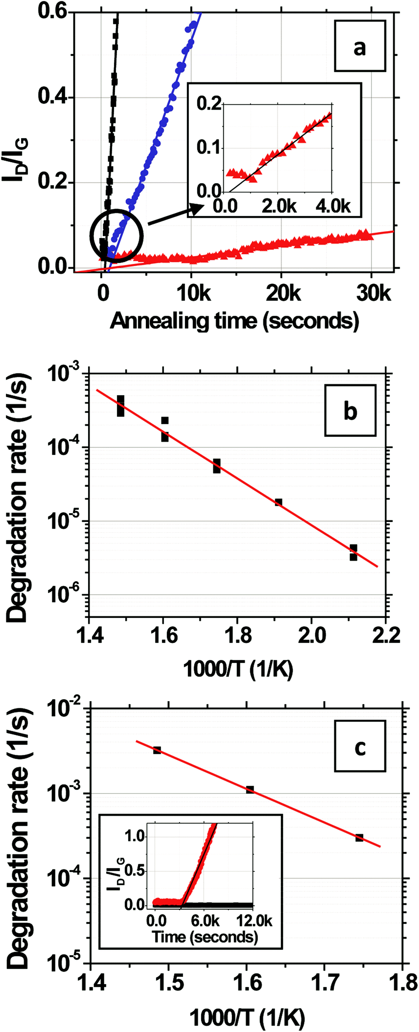 | ||
| Fig. 3 Rate and kinetics of degradation of monolayer CVD-graphene on SiO2/Si. (a) Red-triangles, blue-circles and black-squares represent the evolution of ID/IGversus time in humid air (15000 ppm H2O) at 473 K, 573 K and 673 K, respectively. Inset: initial lag in the onset of the linear increase in ID/IG with time. (b) Arrhenius dependence of the degradation rate (∂(ID/IG)/∂t) with temperature (R673 = (3.7 ± 0.7) × 10−4 s−1, EA = 0.63 ± 0.05 eV) for CVD-graphene in humid air (15000 ppm H2O). (c) Arrhenius dependence of the degradation rate (∂(ID/IG)/∂t) with temperature (R673 = (3.2 ± 0.1) × 10−3 s−1, EA = 0.79 ± 0.01 eV) for mechanically exfoliated graphene in humid air (12000 ppm H2O). Inset: comparison of the evolution of ID/IGversus time for single (red) and multiple layers of mechanically exfoliated graphene (black) on SiO2/Si at 623 K. | ||
The above experiment is also performed for mechanically exfoliated graphene transferred onto SiO2/Si to examine whether the initial “quality” of the graphene affects the kinetics or energetics of oxidation (Fig. 1i). Unlike the mechanically exfoliated graphene, the CVD graphene is stitched together via defective grain boundaries. In addition, the superior transport characteristics of exfoliated graphene29,30 suggest that the initial concentration of defects is lower in exfoliated graphene than in CVD graphene grown on Cu foils under the conditions used here. Moreover, mechanically exfoliated graphene is also flatter and single crystalline whereas the topology of CVD-grown graphene contains wrinkles and maintains the memory of the “rough” Cu foil catalyst substrates and is polycrystalline (average grain size here is ∼14 μm). The ID/IG for mechanically exfoliated monolayer graphene is measured over a smaller area of 2 × 2 μm2 away from the edges of the flakes because of their limited size, in humid air at a water vapor concentration of ∼12000 ppm. The fit R673 = (3.2 ± 0.1) × 10−3 s−1 and EA = 0.79 ± 0.01 eV (Fig. 3c). While the small 20% difference in water vapor concentration between the experiments on CVD-graphene and mechanically exfoliated graphene precludes precise quantitative comparison, the relatively low EA for both cases (compared with the much higher EA measured in dry air below), indicates that the “quality” of the graphene and intrinsic defects do not substantially lower the effective EA in humid air on SiO2/Si substrates. Rather, these data indicate the importance of extrinsic factors, for example graphene–substrate interactions, in driving the degradation.
In contrast to single layer graphene, mechanically exfoliated few (1 < n < 4) layer graphene transferred to SiO2/Si is much more stable in humid air. The inset in Fig. 3c compares the evolution of ID/IGversus time for single and multiple layers of graphene on SiO2/Si at 623 K. Whereas ID/IG for the single layer increases rapidly with time, ID/IG for multiple layers does not measurably increase even after 3 hours. In both cases, the top layer of graphene is hot and exposed to the humid air. However, in the few layer sample, the top layer that is exposed to the humid air is isolated from the SiO2 substrate by the underlying layers, which themselves are not directly exposed to the ambient environment. Thus, graphene isolated from the SiO2 substrate oxidizes and gasifies very slowly even in humid air. These results suggest that substrate interactions play important roles in the degradation of single layers of graphene. While we cannot preclude the possibility that bi- or multi-layer graphene might be less reactive than single layer graphene, even in the absence of substrate-effects, it is well known that the different layers are coupled via a weak van der Waals interaction with only minor electronic perturbation. Taking this argument into account, the most likely explanation for the decreased reactivity of the topmost layer of the multi-layer graphene is the isolation from the substrate. This explanation is further supported by the qualitative study of the chemical reactivity of graphene on various substrates by Yamamoto et al.11
It has been theoretically shown by Patra et al. that water can act as a catalytic element that initiates rapid conformational changes in single layers of graphene.21 Also, experimental studies indicate that water has the ability to intercalate at the graphene–SiO2 interface and deform the surface of the atomic membrane.19,22 These effects distort the graphene on the atomic scale creating deformation or curvature causing strain-induced pyramidalization, which is known to increase the chemical reactivity.31 Therefore cumulatively, it can be hypothesized that the critical role of water on oxides may be to strain and deform single layers of graphene thereby decreasing the activation energy for oxidation (Fig. 1i).
To probe the effect of water vapor further, we next study the effect of reducing its concentration on the degradation rate and activation energy. In this case, we use the closed-lid setup and dry the wet ambient air using desiccants. The use of desiccants has the advantage of ensuring that the composition of the ambient air remains constant except for water vapor, which is reduced by the desiccants (as opposed to creating mixtures of dry N2 and O2 that are missing the other relevant components of an ambient atmosphere like CO and CO2). In the closed-lid setup, the humid ambient air is drawn through 3 cascaded drying tubes of desiccants (1× silica gel, Fisher Chemical product # S161-500 and 2× drierite, W.A. Hammond Drierite Indicating Drying Tube 8′′L × 3/4′′ O.D.) and then through the sample chamber by pulling vacuum on the outlet port of the sample chamber. This approach reduces the water vapor concentration below the sensitivity of our hygrometer to <2000 ppm. We also conduct a control experiment in the closed-lid setup using humid air without desiccants to test whether the flow of the gas over the substrate used in this closed-lid setup leads to differences in degradation compared to the open-lid setup used previously in which there was no forced flow. The humid air (water vapor concentration ∼15000 ppm) in the closed-lid setup yields a R673 = (7.8 ± 1.0) × 10−4 s−1 and an EA = 0.71 ± 0.06 eV (Fig. 4a), which is similar to the EA of 0.63 ± 0.05 determined previously in the open-lid setup.
 | ||
| Fig. 4 (a) Arrhenius dependence of the degradation rate ((∂(ID/IG)/∂t) with temperature of monolayer CVD-graphene on SiO2/Si in humid air (blue-squares) and in desiccated-dry air (red-circles). EA = 0.71 ± 0.06 eV and EA = 1.85 ± 0.17 eV for CVD-graphene in humid air and desiccated-dry air, respectively. (b) Represents the evolution of ID/IGversus time in nitrogen (99.999%) for monolayer CVD-graphene on SiO2/Si at 623 K. | ||
The degradation rate is substantially slower in dry air. At 623 K, it is 100 times slower. The activation energy increases to EA = 1.85 ± 0.17 eV (Fig. 4a) with R673 = (3.6 ± 0.4) × 10−5 s−1, which is ∼3 times EA in humid air. Both the above observations with the dry air indicate that water vapor present in the air plays a vital role in the degradation process on SiO2 which is consistent with the theoretical studies and qualitative observations made regarding conformational changes in the graphene on SiO2 in humid but not dry air by other groups.19–22 A previous study has shown that water vapor can independently abstract C atoms from the basal plane of graphite thereby creating new defects on the surface between 673 and 1573 K;32 however, this effect seems to be secondary to substrate effects as evidenced by immeasurably slow degradation of the few layered graphene samples on SiO2 in humid air (inset, Fig. 3c).
To further investigate the thermal stability of single layers of graphene on SiO2, we measure the evolution of ID/IG under a nitrogen atmosphere (99.999% N2, <1 ppm O2, <1 ppm water vapor). As shown in Fig. 4b, no measurable degradation is observed at 623 K even after 7 hours of annealing, indicating that the quality of the graphene is unaffected even at elevated temperatures under inert conditions similar to what has been previously reported by several groups.33–38
2.2. Ex situ spatially-resolved imaging Raman spectroscopy (IRS)
Now that the rate and the activation energy for the oxidation of single layers of graphene on SiO2 are known, we next investigate and visualize the degradation using imaging Raman spectroscopy (IRS) and electron microscopy. To compare the contribution to ID/IG from grain boundaries versus grain interiors, we imaged its spatial distribution using IRS at different times at 623 K in humid air. Fig. 5a and b (insets) show optical images of the regions of graphene on SiO2/Si scanned after annealing for 45 and 110 minutes, respectively. Etching and gasification along grain boundaries and smaller circular features (etch pits) are evident from the optical images. The IRS maps of these same areas are shown in Fig. 5a and b. After 45 minutes (Fig. 5a), the ID/IG is most intense at the grain boundaries. The graphene that has been etched and gasified at the grain boundaries (Fig. 1iii and iv) no longer contributes to this ID/IG because this carbon has been removed as CO and CO2, but rather the carbon remaining at the edges of the graphene grains gives rise to the intense ID/IG signal. More importantly, substantial oxidation (Fig. 1i) has also occurred within the grains. The average ID/IG at the grain boundaries (determined by averaging ID/IG ± 0.4 μm along each grain boundary) is 0.80 whereas the average ID/IG in the remaining grain interiors is 0.23. Even though ID/IG at the grain edges is higher, the area occupied by the grain interiors is much larger; therefore the ID/IG spatially averaged over the entire image (= 0.4) is actually dominated by the grain interiors. For example, spatially weighing, we find that 70% of the overall ID/IG comes from the interiors whereas only 30% of the ID/IG comes from the grain boundaries. Moreover, the ID/IG at the grain edges should remain invariant with time because new oxidation at the grain edges is accompanied by new gasification, as discussed in section 2.3 below. Thus, the spatially averaged data and activation energies presented in section 2.1 are indicative of the oxidation (Fig. 1i) that occurs within the grains. After 110 minutes (Fig. 5b), the ID/IG at the grain interiors and the grain edges becomes indistinguishable and the integrated average of the ratio becomes ∼1.0. The above results again highlight that the deterioration proceeds via two different processes that occur with different kinetics: (a) the oxidation of the grain interiors (Fig. 1i) and (b) oxidation and gasification at grain boundaries and edges (Fig. 1iii and iv). Whereas the kinetics of the oxidation of the grain interiors are quantified via Raman spectroscopy above, the kinetics of the oxidation and gasification of grain edges are quantified in section 2.3 below. | ||
| Fig. 5 Temporally resolved imaging Raman spectroscopy depicting the progression of the degradation process. (a) depicts the spatial distribution of ID/IG over regions of visibly etched grain boundaries (as seen in the inset) after 45 min of annealing in humid air (15000 ppm H2O) at 623 K and (b) depicts the same after 110 minutes of annealing (inset scalebars = 5 μm). (c) represents the evolution of ID/IGversus time in humid air (15000 ppm H2O) 623 K, where dotted-circles ‘a’ and ‘b’ denote the instances corresponding to (a) and (b) above. | ||
2.3. Temperature dependence of the grain boundary etch rate
We next use time-resolved scanning electron microscopy (SEM) to quantify and image the gasification process at the grain edges. A single layer of CVD-grown graphene is transferred to SiO2/Si and split into several smaller pieces. The samples are maintained at a constant temperature (673 K) in humid air (water vapor = 15000 ppm) in the open-lid Raman chamber and removed at intervals of 15 minutes and then imaged by the SEM as shown in Fig. 6. The first visually obvious signatures of etching are at (i) grain-boundaries in the graphene (orange dashed lines), (ii) linear striations in the graphene (black dashed lines), which are spatially commensurate with rough, linear striations in the Cu foil growth substrate that arise from its manufacture, and (iii) random spots (yellow encircled feature) in the graphene grain interiors presumably from point/other surface defects that are present in the as-grown graphene. With time (Fig. 6) these etch pits and lines grow wider. Our observations are consistent with previous experimental and theoretical studies where it has been shown that graphitic materials selectively etch or oxidize at intrinsic and induced defects.13,39–41 The dark lines in Fig. 6 are wrinkles or folds in the graphene layer which originate from a mismatch between the thermal expansion coefficient of the atomic membrane and the Cu substrate.42 It can be noted that these folds etch relatively slowly and are more stable (Fig. 6a–d), presumably because they are elevated off the SiO2 substrate.43 It is important to note that the scale of these wrinkles and folds is much larger than the atomic-scale deformation induced by water-mediated interactions with the substrate. While the latter deformation occurs over a few lattice constants of graphene leading to an increased reactivity, the former deformation via wrinkling and folding occurs over a much longer length scale and elevates the graphene off the substrate thereby increasing its oxidative stability.
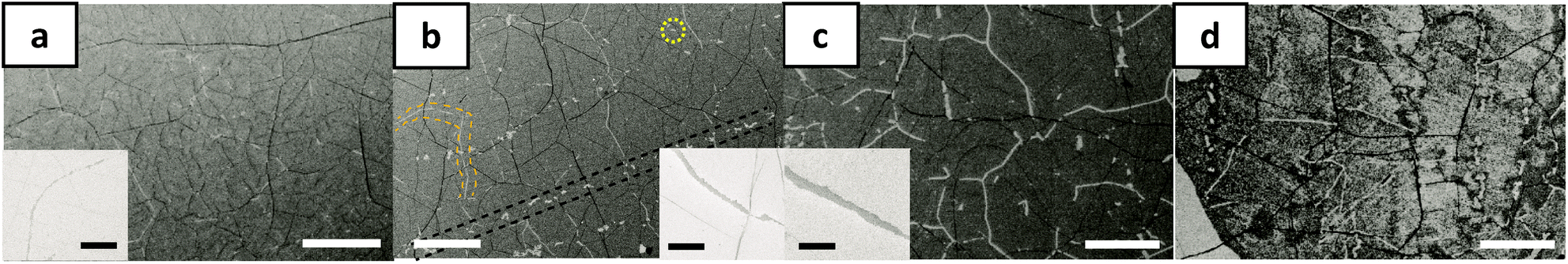 | ||
| Fig. 6 Evolution of etching of monolayer CVD-graphene on SiO2/Si: (a), (b), (c) and (d) represent 15, 30, 45 and 60 minute etch periods in humid air (15000 ppm H2O) at 673 K (white scalebars = 10 μm and black scalebars = 1 μm). Contrast of the etched grain boundaries is reversed in the insets due to charging and deposition of carbon on the SiO2 substrate which is commonly observed during high magnification imaging in the scanning electron microscope. (b) also shows the first visually obvious signatures of etching at (i) grain boundaries in the graphene (orange dashed lines), (ii) linear striations in the graphene (black dashed lines), which are spatially commensurate with rough, linear striations in the Cu foil, and (iii) random spots (yellow encircled feature) in the graphene grain interiors presumably from point/other surface defects that are present in the as-grown graphene. | ||
We capture electron micrographs as a function of time and temperature and calculate the average etch-width of the grain boundaries over a cumulative-length of >200 μm using an image analysis algorithm. From these data, we are able to calculate the etch rate at a grain boundary edge at a given temperature and also the temperature dependence of this rate and the activation energy. The histograms in Fig. 7a–c show the frequency distribution of the grain boundary widths after 240, 105, and 45 minutes of etching at 573, 623, and 673 K, respectively. From the mode of these distributions fit to log-normal distributions, we find that the grain edges etch with a mode velocity of 3.6 × 10⁻³, 2.3 × 10⁻², and 1.1 × 10⁻¹ nm s−1 at 573, 623, and 673 K, respectively. The temperature dependence of the mode velocity can be represented by v = v673exp[(−EA/kB)(1/T − 1/673)] with v673 = (1.08 ± 0.02) × 10−1 nm s−1 and EA = 1.14 ± 0.10 eV. Several previous studies have investigated the analogous gasification of graphite from crystal edges, reporting large variations in the measured EA from 0.7 to 2.0 eV.14,32,44–46 However, differences in the experimental O2 and H2O concentrations and the temperature range between our study and these past studies of graphite make direct comparison difficult. Whereas the EA of 0.63 ± 0.05 eV measured in section 2.1 quantifies the activation energy for the oxidation (Fig. 1i) of the grain interiors, the EA of 1.14 ± 0.10 eV measured in this section quantifies the activation energy for the gasification of the grain edges (Fig. 1iv).
 | ||
| Fig. 7 Temperature dependence of the grain boundary etch rate: (a), (b), and (c) represent the frequency distribution of the grain boundary widths after 240, 105, and 45 minutes of etching at 573, 623, and 673 K, respectively, fit to a log-normal curve. The fits from (a), (b) and (c) are used to determine the etch rates at the respective temperatures and (d) depicts the Arrhenius dependence of these rates on the temperature (EA = 1.14 ± 0.10 eV). | ||
Sections 2.1–2.3, combined, allow us to paint a more detailed picture of the degradation of graphene monolayers, which occurs via a two-step process: oxidation followed by gasification as CO or CO2. Our data show that the barrier for the oxidation of pristine grain interiors (Fig. 1i) is lowered to 0.63 ± 0.05 eV in humid air on SiO2 substrates. Theory has also shown that the pre-existing point (e.g. vacancy) and graphene edges (Fig. 1iii) will oxidize in air in a barrierless process.14 Thus, pre-existing defects and the pristine grain interiors will oxidize, with either no barrier or a small 0.63 eV barrier, respectively, relatively rapidly even at a modest temperature. It is thought that adsorbed oxygen molecules will dissociate to form oxygen based stationary functional groups like –C![[double bond, length as m-dash]](https://www.rsc.org/images/entities/char_e001.gif) O, –C–O, –O–CO etc. and sometimes mobile/floating functional groups like C–O–C.16–18,47–49 The gasification of oxidized carbon atoms can next occur in the form of CO or CO2 gas through several probable reaction pathways depending on the stationary functional group of the carbon atom and its proximity to mobile functional groups.14,16–18,47,50 Gasification leads to widening/etching of the grain edges and boundaries (Fig. 1iv), as seen previously in the SEM images (Fig. 6), with an EA of 1.14 ± 0.10 eV. The Raman ID/IG data indicate that the density of oxidized carbon atoms increases with time within the grain interiors; however, our measurements do not directly tell us the activation energy for the gasification (Fig. 1ii) of these oxidized carbon atoms. With this said, gasification from within the grain interiors will eventually lead to the formation of small etch pits, and gasification from the edges of these etch pits will also be dictated by an EA of 1.14 ± 0.10 eV.
O, –C–O, –O–CO etc. and sometimes mobile/floating functional groups like C–O–C.16–18,47–49 The gasification of oxidized carbon atoms can next occur in the form of CO or CO2 gas through several probable reaction pathways depending on the stationary functional group of the carbon atom and its proximity to mobile functional groups.14,16–18,47,50 Gasification leads to widening/etching of the grain edges and boundaries (Fig. 1iv), as seen previously in the SEM images (Fig. 6), with an EA of 1.14 ± 0.10 eV. The Raman ID/IG data indicate that the density of oxidized carbon atoms increases with time within the grain interiors; however, our measurements do not directly tell us the activation energy for the gasification (Fig. 1ii) of these oxidized carbon atoms. With this said, gasification from within the grain interiors will eventually lead to the formation of small etch pits, and gasification from the edges of these etch pits will also be dictated by an EA of 1.14 ± 0.10 eV.
It is likely that the barrier to the oxidation of pristine grain interiors is lowered in humid air on SiO2 substrates because the roughness of the SiO2 substrate introduces local deviations in the sp2 structure (as observed in previous AFM studies)9,11 and because of charge inhomogeneity11,25 on the SiO2 substrate. This hypothesis can be further verified qualitatively from a bilayer experiment in Fig. 3c, where the topmost graphene layer is isolated from the substrate, resulting in a significantly slower degradation. The lower activation energy calculated for the interior oxidation (Fig. 3) compared to the one calculated for grain boundary etching (Fig. 7) indicates that the build-up of defects is faster (Fig. 1i) than the removal of carbon atoms via gasification (Fig. 1iv), which is why the graphene grains appear to disappear from the inside out in Fig. 6d.
2.4 In situ temperature-dependent field-effect transport measurements
Finally, in order to assess the effects of degradation on the electronic properties of graphene on SiO2, we use field effect transistor measurements to quantify both the doping concentration and charge carrier mobility of single layers of CVD-grown graphene in situ during degradation between 473 K and 673 K in humid air (water vapor = 15000 ppm). Prior to annealing, the CVD-grown graphene is p-type doped with a carrier concentration of 2.4 × 1013 cm−2 and a field-effect mobility, μ, of 500 cm2 V−1 s−1, at room temperature. The carrier concentration is determined by extrapolating the linear portion of the source–drain current versus gate bias transfer curve to zero-current to determine the charge neutrality gate bias, and μ is determined from the transconductance, using a standard parallel-plate capacitor model. These fit parameters are typical of graphene grown by CVD on Cu and transferred to SiO2/Si using similar conditions.30,51–53
Fig. 8 shows the evolution of the transconductance characteristics of monolayer graphene on SiO2 at 523 K in ambient air with time. The mobility, determined from the slope of the curve, increases rapidly to a maximum value and then starts decreasing back again with time. During the very beginning stages of annealing, the doping concentration rapidly decreases while μ increases as shown for 523 K in Fig. 9a and b, respectively. These changes can be attributed to the desorption of surface contaminants, which act as charge transfer dopants and charge scattering sites. Following this desorption, the graphene begins to degrade leading to a doping concentration that increases approximately linearly and μ that decreases with time. Our hypothesis is that μ decays mostly due to interior grain oxidation (Fig. 1i), which is based on the observation that the grains oxidize most rapidly from the interior (section 2.2) and the activation energy for this degradation (section 2.1) is lower than that of grain boundary gasification (section 2.3). Previous experiments have shown that the mobility of exfoliated monolayer graphene decays inversely with point defect density.28,54 Accordingly, we fit our μ decay data to the following form μ−1 = μ0−1 + λ(t − to), where μ0 is the mobility prior to degradation, to is the time at which the degradation begins, and λ is the decay constant, which will be proportional to the point defect generation rate (Fig. 9b). λ is computed by calculating the slope of the μ−1vs. annealing time plot (Fig. 9b) at μ = 500 cm2 V s−1, which is around the center of the range where μ exhibits an almost linear behavior. The fit decay constant λ increases with temperature as shown in Fig. 9c, varying as λ = λ673exp[(−EA/kB)(1/T − 1/673)] with temperature where λ673 = (1.1 ± 0.3) × 10−5 cm−2 V and EA = 0.66 ± 0.08 eV (Fig. 9c). The mobility dependent decay time can be defined as τ(μ) = 1/(λμ). In particular, at 523 K, the mobility dependent decay time at μ = 500 cm2 V s−1 is τ = 3.6k s. It can be noted that μ−1 does not have an exact linear dependence on time. The non-linearity can be attributed to other mechanisms, for example the opening of grain boundaries.
 | ||
| Fig. 8 Sheet conductance vs. gate voltage characteristics of monolayer graphene on SiO2 at 523 K vs. time. Top to bottom represents the transconductance characteristics at (i) t = 0 s (black), (ii) 300 s (red), (iii) 3500 s (blue) and (iv) 6200 s (pink). | ||
 | ||
| Fig. 9 Effect of degradation on transport properties of graphene: (a) and (b) represent the evolution of the charge concentration and carrier mobility, respectively, with time at 523 K for the CVD-graphene based FET devices on SiO2/Si. Mobility vs. time plots for different temperatures are independently fit to compute the decay constants for each temperature. (c) depicts the Arrhenius dependence of the decay constant, λ, determined from the exponential decay on temperature, where λ = λ673exp[(−EA/kB)(1/T − 1/673)] and where λ673 = (1.1 ± 0.3) × 10−5 cm−2 V and EA = 0.66 ± 0.08 eV. | ||
3. Implications and conclusions
Successful integration and support of monolayer graphene on substrates, especially oxides, is an integral part of realizing electronic and optoelectronic devices with an atomic membrane. We find that the grain interiors of monolayer graphene oxidize at a rate (∂/∂t)(ID/IG) = R673exp[(−EA/kB) (1/T − 1/673)]. In humid ambient air (15000 ppm H2O), CVD-graphene has a R673 = (3.7 ± 0.7) × 10−4 s−1 and an EA = 0.63 ± 0.05 eV, whereas in dry air R673 = (3.6 ± 0.4) × 10−5 s−1 and EA = 1.85 ± 0.17 eV. Mechanically exfoliated monolayer graphene oxidizes with similar kinetics to CVD-grown monolayer graphene. The degradation is immeasurable for exfoliated multilayers in ambient air and for CVD-monolayers in nitrogen. Etching at the grain boundaries for monolayers proceeds with a mode velocity v = v673exp[(−EA/kB){(1/T) − (1/673)}] with v673 = (1.08 ± 0.02) × 10−1 nm s−1 and EA = 1.14 ± 0.10 eV. At a given temperature, the charge carrier mobility decay rate is given by μ−1 = μ0−1 + λ(t − to), and the decay constant varies as λ = λ673exp[(−EA/kB)(1/T − 1/673)] where λ673 = (1.1 ± 0.3) × 10−5 cm−2 V and EA = 0.66 ± 0.08 eV.
These measurements are useful for two important reasons. Firstly, these measurements can be used to quantitatively predict the oxidative stability of monolayer graphene on SiO2 under different conditions. For example, at 298 K in humid (15000 ppm H2O) ambient air, (∂/∂t)(ID/IG), v, and τ (500 cm2 V−1 s−1) can be extrapolated to 4.5 × 10⁻¹⁰ s−1, 7.3 × 10⁻⁵ nm per year and 8.4 year, respectively. Thus, the mobility of graphene exposed to humid ambient air on SiO2 is expected to be stable at room temperature for only a duration of several years. At an elevated temperature of 380 K the same parameters become 4.49 × 10⁻⁸ s−1, 1 nm per year, and 12.4 days, respectively. Under these conditions, mobility decay is much faster and the grain boundaries will etch leaving discontinuous graphene after roughly one year.
Secondly, these data are useful as they clearly show how graphene's stability on SiO2 can be increased. Most importantly, graphene's stability on SiO2 in ambient air can be improved by limiting its exposure to water vapor. Furthermore, degradation at grain boundaries or striations can be reduced by growing graphene with larger grains and using high quality, flatter metal catalyst substrates, respectively. Ultimately, this study is expected to serve as a foundation for overcoming the limitations posed by ambient air on graphene and help engineer graphene materials with superior properties for demanding applications.
4. Experimental details
4.1. CVD-graphene growth
Monolayers of graphene were grown on Cu foils (Alfa Aesar product# 13382, lot# B03Y027) as the growth catalyst. The foils were pre-cleaned with acetic acid (Fisher) for 15 minutes to remove contaminants and native oxides and then rinsed in DI water (×3) before being dried with an air-gun. The cleaned Cu foils were then annealed for 30 minutes at 1030 °C in 95% argon + 5% hydrogen (340 sccm flow rate) to remove trace surface contaminants and also to reduce the surface roughness of the foil before initiating the growth process. The growth was conducted at 1030 °C with 95% argon + 5% methane (0.300 sccm) and 95% argon + 5% hydrogen (340 sccm) for 3 hours. The manufactured graphene on Cu foils was stored in a N2 glovebox to prevent the oxidation of the graphene and the copper surfaces. All the graphene monolayers used for the experiments were manufactured from the same batch for consistency and the initial ID/IG varied as 0.06 ± 0.025 for the entire batch used for this study.4.2. Transfer of CVD-graphene onto SiO2/Si and mechanical exfoliation of graphene
Graphene monolayers grown via CVD were transferred on to Si substrates with an 89 nm thick thermally-grown SiO2 layer. The transfer was completed using a commonly employed sacrificial polymer (PMMA – poly methyl methacrylate) method, similar to what has been previously reported.8,27 CVD-graphene on copper was over-coated with PMMA (MW = 950k, 2% in chlorobenzene) by spin-coating at 2000 rpm. The samples were placed in the copper etchant ammonium persulfate (25% Transene company, Inc. APS-100 + 75% DI water) and then ultrasonicated for 15 minutes to remove the bottom-facing graphene layer. The samples were left overnight (∼10 h) in the etchant for the copper for complete etching. Post-etching, the floating PMMA on graphene was scooped out from the APS solution and re-floated in DI water (×3) to remove any residual copper etchant. The samples were then dispersed in 5% HF in DI water for 60 minutes to remove trace silica particles that might have deposited from the CVD system during the growth, following which they were rinsed in DI water (×3). From the final DI water bath, the samples were scooped onto SiO2/Si and spin-dried at 8000 rpm for 2 minutes to remove water trapped between the graphene sheet and the substrate. To remove the PMMA layer, the samples were placed in room-temperature acetone baths (×2) for 20 minutes after which they were rinsed in isopropanol for 2 minutes to wash away any residual acetone. Finally, they were dried using an air-gun before being cut into several pieces for further analysis.Mechanical exfoliation of monolayer graphene on SiO2 was done from small flakes of HOPG using the scotch-tape method that has been previously used in several other studies, and they were identified on the substrate using optical microscopy and further confirmed via Raman spectroscopy.55,56 The thickness of silicon dioxide, 89 nm, used in the experiments creates enough contrast between the graphene and the substrate to make the graphene visible under white light in an optical microscope. In particular, the lowest contrast features indicate the presence of a single graphene layer and addition of subsequent layers increases this contrast and makes it appear darker, progressively. In the Raman spectra for an intrinsically doped monolayer graphene on SiO2/Si, (i) the 2D-band to G-band ratio is always >1 at a 532 nm excitation wavelength and (ii) the 2D peak can be fitted to a single Lorentzian function. For a bi-layer graphene the 2D to G band ratio is <1 and the 2D peak can be fitted to two Lorentzian functions.57,58
4.3. Characterization and analysis techniques
(i) In situ Raman spectroscopy: Labram Aramis by Horiba was used for the in situ Raman studies. An enclosed heating stage (Linkam THMS 600) was integrated with an automated X–Y stage to control the temperature of the sample and atmosphere around it. A 532 nm laser with power = 1 mW and exposure time = 1 s per spot was used for all the scans to avoid substrate heating effects. Maps were collected across a fixed 100 μm × 100 μm region (with a pixel size of 10 μm × 10 μm) at intervals of 150 seconds during the annealing period. A temperature controller was used to control the initial ramp-rate (100 K min−1) and the final hold-temperature of the stage. Gas inlets in Linkam THMS 600 were used to pump or purge the sample chamber to control the atmosphere. The heating rate used for all the measurements was 100 °C min−1 and the measurements of relative humidity and Raman spectra were initiated after the stage had reached the set annealing temperature.(ii) Imaging Raman spectroscopy: MicroRaman DXR from Thermofisher was used for all the spatially-resolved Raman imaging studies. A 532 nm laser with power = 1 mW and exposure time = 3 s per spot was used for all the scans to avoid substrate heating effects. The laser spot size was focused to ∼700 nm, and a mapping pixel size of 200 nm × 200 nm was used.
(iii) Scanning electron microscopy: SEM LEO 1530 was used to image the graphene on SiO2/Si samples. The electron gun energy used was 3 keV.
(iv) Image analysis: The scanning electron micrographs were analyzed via an image analysis algorithm developed using MATLAB to compute the average grain boundary width.
(v) Charge carrier mobility measurements: Graphene based field-effect transistors were made with 89 nm SiO2 as the gate dielectric on a Si gate. 75 nm of Au was thermally evaporated through a shadow mask to form the source and drain contacts. The channel width and length were 5 mm and 1 mm, respectively. The temperature was controlled using a Linkam THMS 600 during the measurements. The heating rate used for all the measurements was 100 °C min−1 and the transconductance measurements were initiated after the stage had reached the set annealing temperature.
Acknowledgements
The majority of the experimental Raman spectroscopy and electron microscopy work was supported by the National Science Foundation (grant number CBET-1033346). The experimental Raman spectroscopy and electron microscopy were partially supported by Wisconsin Energy Institute. The in situ charge transport measurements were supported by the DOE Office of Science Early Career Research Program (grant number DE-SC0006414) through the Office of Basic Energy Sciences. The grain boundary etching analysis was supported by the University of Wisconsin-Madison, Center of Excellence for Materials Research and Innovation (National Science Foundation grant number DMR-1121288). MSA also acknowledges partial support from a 3M Non-Tenured Faculty Grant. The authors gratefully acknowledge the use of facilities and instrumentation supported by the NSF-funded University of Wisconsin Materials Research Science and Engineering Center (DMR-1121288).References
- H. E. Romero, N. Shen, P. Joshi, H. R. Gutierrez, S. A. Tadigadapa, J. O. Sofo and P. C. Eklund, ACS Nano, 2008, 2, 2037–2044 CrossRef CAS PubMed.
- C. A. Di, D. C. Wei, G. Yu, Y. Q. Liu, Y. L. Guo and D. B. Zhu, Adv. Mater., 2008, 20, 3289–3293 CrossRef CAS.
- Z. G. Cheng, Q. Y. Zhou, C. X. Wang, Q. A. Li, C. Wang and Y. Fang, Nano Lett., 2011, 11, 767–771 CrossRef CAS PubMed.
- F. N. Xia, T. Mueller, Y. M. Lin, A. Valdes-Garcia and P. Avouris, Nat. Nanotechnol., 2009, 4, 839–843 CrossRef CAS PubMed.
- H. Y. Nan, Z. H. Ni, J. Wang, Z. Zafar, Z. X. Shi and Y. Y. Wang, J. Raman Spectrosc., 2013, 44, 1018–1021 CrossRef CAS.
- S. Singha Roy and M. Arnold, Adv. Funct. Mater., 2013, 23, 3638–3644 CrossRef.
- L. Liu, S. Ryu, M. R. Tomasik, E. Stolyarova, N. Jung, M. S. Hybertsen, M. L. Steigerwald, L. E. Brus and G. W. Flynn, Nano Lett., 2008, 8, 1965–1970 CrossRef CAS PubMed.
- S. S. Roy, D. J. Bindl and M. S. Arnold, J. Phys. Chem. Lett., 2012, 3, 873–878 CrossRef PubMed.
- M. Ishigami, J. H. Chen, W. G. Cullen, M. S. Fuhrer and E. D. Williams, Nano Lett., 2007, 7, 1643–1648 CrossRef CAS PubMed.
- R. Sharma, J. H. Baik, C. J. Perera and M. S. Strano, Nano Lett., 2010, 10, 398–405 CrossRef CAS PubMed.
- M. Yamamoto, T. L. Einstein, M. S. Fuhrer and W. G. Cullen, ACS Nano, 2012, 6, 8335–8341 CrossRef CAS PubMed.
- P. Solis-Fernandez, J. I. Paredes, S. Villar-Rodil, L. Guardia, M. J. Fernandez-Merino, G. Dobrik, L. P. Biro, A. Martinez-Alonso and J. M. D. Tascon, J. Phys. Chem. C, 2011, 115, 7956–7966 CAS.
- J. D. Jones, C. F. Morris, G. F. Verbeck and J. M. Perez, Appl. Surf. Sci., 2013, 264, 853–863 CrossRef CAS.
- J. R. Hahn, H. Kang, S. M. Lee and Y. H. Lee, J. Phys. Chem. B, 1999, 103, 9944–9951 CrossRef CAS.
- J. Zhang, H. L. Zou, Q. Qing, Y. L. Yang, Q. W. Li, Z. F. Liu, X. Y. Guo and Z. L. Du, J. Phys. Chem. B, 2003, 107, 3712–3718 CrossRef CAS.
- K. Sendt and B. S. Haynes, Proc. Combust. Inst., 2005, 30, 2141–2149 CrossRef.
- K. Sendt and B. S. Haynes, Combust. Flame, 2005, 143, 629–643 CrossRef CAS.
- K. Sendt and B. S. Haynes, J. Phys. Chem. C, 2007, 111, 5465–5473 CAS.
- M. J. Lee, J. S. Choi, J.-S. Kim, I.-S. Byun, D. H. Lee, S. Ryu, C. Lee and B. H. Park, Nano Res., 2012, 5, 710–717 CrossRef CAS.
- L. Liu, D. Xie, M. Wu, X. Yang, Z. Xu, W. Wang, X. Bai and E. Wang, Carbon, 2012, 50, 3039–3044 CrossRef CAS.
- N. Patra, B. Wang and P. Kral, Nano Lett., 2009, 9, 3766–3771 CrossRef CAS PubMed.
- D. Lee, G. Ahn and S. Ryu, J. Am. Chem. Soc., 2014, 136, 6634–6642 CrossRef CAS PubMed.
- L. G. Cancado, A. Jorio, E. H. Martins Ferreira, F. Stavale, C. A. Achete, R. B. Capaz, M. V. O. Moutinho, A. Lombardo, T. S. Kulmala and A. C. Ferrari, Nano Lett., 2011, 11, 3190–3196 CrossRef CAS PubMed.
- A. Jorio, E. H. Martins Ferreira, M. V. O. Moutinho, F. Stavale, C. A. Achete and R. B. Capaz, Phys. Status Solidi B, 2010, 247, 2980–2982 CrossRef CAS.
- R. Decker, Y. Wang, V. W. Brar, W. Regan, H.-Z. Tsai, Q. Wu, W. Gannett, A. Zettl and M. F. Crommie, Nano Lett., 2011, 11, 2291–2295 CrossRef CAS PubMed.
- A. Eckmann, A. Felten, I. Verzhbitskiy, R. Davey and C. Casiraghi, Phys. Rev. B: Condens. Matter, 2013, 88, 035426 CrossRef.
- X. Li, Y. Zhu, W. Cai, M. Borysiak, B. Han, D. Chen, R. D. Piner, L. Colombo and R. S. Ruoff, Nano Lett., 2009, 9, 4359–4363 CrossRef CAS PubMed.
- J.-H. Chen, W. G. Cullen, C. Jang, M. S. Fuhrer and E. D. Williams, Phys. Rev. Lett., 2009, 102, 215504 Search PubMed.
- K. I. Bolotin, K. J. Sikes, Z. Jiang, M. Klima, G. Fudenberg, J. Hone, P. Kim and H. L. Stormer, Solid State Commun., 2008, 146, 351–355 CrossRef CAS.
- A. Venugopal, J. Chan, X. Li, C. W. Magnuson, W. P. Kirk, L. Colombo, R. S. Ruoff and E. M. Vogel, J. Appl. Phys., 2011, 109, 104511 CrossRef.
- S. Niyogi, M. A. Hamon, H. Hu, B. Zhao, P. Bhowmik, R. Sen, M. E. Itkis and R. C. Haddon, Acc. Chem. Res., 2002, 35, 1105–1113 CrossRef CAS PubMed.
- X. Chu and L. D. Schmidt, Surf. Sci., 1992, 268, 325–332 CrossRef CAS.
- K. Kim, W. Regan, B. Geng, B. Aleman, B. M. Kessler, F. Wang, M. F. Crommie and A. Zettl, Phys. Status Solidi RRL, 2010, 4, 302–304 CrossRef CAS.
- W. A. de Heer, C. Berger, X. S. Wu, P. N. First, E. H. Conrad, X. B. Li, T. B. Li, M. Sprinkle, J. Hass, M. L. Sadowski, M. Potemski and G. Martinez, Solid State Commun., 2007, 143, 92–100 CrossRef CAS.
- C. Berger, Z. M. Song, T. B. Li, X. B. Li, A. Y. Ogbazghi, R. Feng, Z. T. Dai, A. N. Marchenkov, E. H. Conrad, P. N. First and W. A. de Heer, J. Phys. Chem. B, 2004, 108, 19912–19916 CrossRef CAS.
- S. Shivaraman, M. V. S. Chandrashekhar, J. J. Boeckl and M. G. Spencer, J. Electron. Mater., 2009, 38, 725–730 CrossRef CAS.
- L. Blackberg, A. Ringbom, H. Sjostrand and M. Klintenberg, Phys. Rev. B: Condens. Matter, 2010, 82, 4 CrossRef.
- J. Chen, T. Shi, T. Cai, T. Xu, L. Sun, X. Wu and D. Yu, Appl. Phys. Lett., 2013, 102, 103107 CrossRef.
- Y. Lin, K. A. Watson, J.-W. Kim, D. W. Baggett, D. C. Working and J. W. Connell, Nanoscale, 2013, 5, 7814–7824 RSC.
- J. G. Radich and P. V. Kamat, ACS Nano, 2013, 7, 5546–5557 CrossRef CAS PubMed.
- B. Wang, Y. S. Puzyrev and S. T. Pantelides, Polyhedron, 2013, 64, 158–162 CrossRef CAS.
- W. J. Zhu, T. Low, V. Perebeinos, A. A. Bol, Y. Zhu, H. G. Yan, J. Tersoff and P. Avouris, Nano Lett., 2012, 12, 3431–3436 CrossRef CAS PubMed.
- S. P. Surwade, Z. T. Li and H. T. Liu, J. Phys. Chem. C, 2012, 116, 20600–20606 CAS.
- E. Loren Fuller and J. M. Okoh, J. Nucl. Mater., 1997, 240, 241–250 CrossRef CAS.
- F. Stevens, L. A. Kolodny and T. P. Beebe, J. Phys. Chem. B, 1998, 102, 10799–10804 CrossRef CAS.
- J. R. Hahn, Carbon, 2005, 43, 1506–1511 CrossRef CAS.
- D. Yafei, N. Shuang, L. Zhenyu and Y. Jinlong, J. Phys.: Condens. Matter, 2013, 25, 405301–405306 CrossRef PubMed.
- L. R. Radovic, A. B. Silva-Tapia and F. Vallejos-Burgos, Carbon, 2011, 49, 4218–4225 CrossRef CAS.
- L. R. Radovic, A. Suarez, F. Vallejos-Burgos and J. O. Sofo, Carbon, 2011, 49, 4226–4238 CrossRef CAS.
- X. Qi, X. Guo and C. Zheng, Appl. Surf. Sci., 2012, 259, 195–200 CrossRef CAS.
- J. Heo, H. J. Chung, S.-H. Lee, H. Yang, D. H. Seo, J. K. Shin, U. I. Chung, S. Seo, E. H. Hwang and S. Das Sarma, Phys. Rev. B: Condens. Matter, 2011, 84, 035421 CrossRef.
- N. S. Safron, M. Kim, P. Gopalan and M. S. Arnold, Adv. Mater., 2012, 24 Search PubMed.
- M. Kim, N. S. Safron, E. Han, M. S. Arnold and P. Gopalan, ACS Nano, 2012, 6, 9846–9854 CrossRef CAS PubMed.
- Z. H. Ni, L. A. Ponomarenko, R. R. Nair, R. Yang, S. Anissimova, I. V. Grigorieva, F. Schedin, P. Blake, Z. X. Shen, E. H. Hill, K. S. Novoselov and A. K. Geim, Nano Lett., 2010, 10, 3868–3872 CrossRef CAS PubMed.
- L. Ciric, A. Sienkiewicz, B. Nafradi, M. Mionic, A. Magrez and L. Forro, Phys. Status Solidi B, 2009, 246, 2558–2561 CrossRef CAS.
- J. S. Bunch, A. M. van der Zande, S. S. Verbridge, I. W. Frank, D. M. Tanenbaum, J. M. Parpia, H. G. Craighead and P. L. McEuen, Science, 2007, 315, 490–493 CrossRef CAS PubMed.
- A. C. Ferrari, J. C. Meyer, V. Scardaci, C. Casiraghi, M. Lazzeri, F. Mauri, S. Piscanec, D. Jiang, K. S. Novoselov, S. Roth and A. K. Geim, Phys. Rev. Lett., 2006, 97, 187401 CrossRef CAS PubMed.
- L. M. Malard, M. A. Pimenta, G. Dresselhaus and M. S. Dresselhaus, Phys. Rep.: Rev. Sec. Phys. Lett., 2009, 473, 51–87 CAS.
| This journal is © The Royal Society of Chemistry 2015 |