
 Open Access Article
 This Open Access Article is licensed under a Creative Commons Attribution-Non Commercial 3.0 Unported Licence
Tuning the deposition of molecular graphene nanoribbons by surface functionalization
R.
Konnerth
a,
C.
Cervetti
ab,
A.
Narita
c,
X.
Feng
c,
K.
Müllen
c,
A.
Hoyer
bd,
M.
Burghard
b,
K.
Kern
bd,
M.
Dressel
a and
L.
Bogani
*ae
a1. Physikalisches Institut, Universität Stuttgart, Pfaffenwaldring 57, D-70550, Stuttgart, Germany
bMax Planck Institut für Festkörperforschung, Heisenbergstraße 1, D-70569 Stuttgart, Germany
cMax Planck Institut für Polymerforschung, Ackermannweg 10, D-55128, Mainz, Germany
dInstitut de Physique de la Matière Condensée, Ecole Polytechnique de Lausanne, CH-1015, Lausanne, Switzerland
eDepartment of Materials, University of Oxford, 16 Parks Road, OX1 3PH, Oxford, UK. E-mail: lapo.bogani@materials.ox.ac.uk
First published on 18th May 2015
Abstract
We show that individual, isolated graphene nanoribbons, created with a molecular synthetic approach, can be assembled on functionalised wafer surfaces treated with silanes. The use of surface groups with different hydrophobicities allows tuning the density of the ribbons and assessing the products of the polymerisation process.
Graphene,1,2 a sheet of carbon atoms arranged in a hexagonal lattice, has attracted immense attention stimulated by both its fundamental properties and its application potential ranging from nano-opto-electronics3 to biosensors4 and spintronics.5 While most experiments have been performed using micrometer-size single flakes,2 several proposals would require the creation of graphene ribbons with nanometer-size width (GNR).6 Perfect control over the width and edge geometry of GNRs might allow creation of novel spintronic devices,7 thermal rectifiers8,9 and homogeneous graphene quantum dots.10 A highly promising way of achieving such a level of control is by bottom-up synthetic approaches, i.e. by polymerising molecular units in a pre-determined pattern, followed by graphitisation. The first successful examples of this approach have only very recently appeared,11–15 with the creation of the first molecular GNRs, which show atomically-regular edges over lengths of more than 500 nm. Such GNRs are an important breakthrough, allowing, for the first time, fine tuning of graphene nanostructures by means of atomic precision of synthetic chemistry.
On the other hand, the assembly and organization of such GNRs, in conditions compatible with the creation of nanoelectronic devices, remains problematic.16 This difficulty has so far prevented the exploitation of the full potential of molecular GNRs in nanoelectronics, and has hindered the observation of the predicted effects. In addition, surface deposition would allow a statistical topographical analysis of the polymerisation reactions, necessary to test and improve the synthetic process and the possible presence of different sub-products.
Here we address this problem by surface functionalization of commercial Si wafers to immobilize and isolate bottom-up synthesized GNRs on surfaces. The devised methodology compatible with the most widespread processes of nanoelectronic fabrication allows tuning the nanoribbons density by changing the surface hydrophobic character.17 Moreover, we provide a full analysis of the depositions, extracting information on the polymerisation processes, on the surface interaction mechanisms and on the Raman signatures.
The GNRs here used are produced by bottom-up synthesis as previously reported12 and have an atomically-defined edge structure, as shown in Fig. 1a. Briefly, they are formed via AB-type Diels–Alder polymerization of monomeric units of 2,5-bis(4-dodecylphenyl)-3-(3-ethynylphenyl)-4-phenyl-2,4-cyclopentadienone, followed by graphitization into graphene nanoribbons via intramolecular oxidative cyclodehydrogenation. The structure of the synthetic GNRs, as obtained via multiple techniques,12 is that of a flat, regular graphene strip, only 3-rings wide, with a “cove-type edge” structure containing dodecyl chains sprouting from it (Fig. 1a). These side chains allow separating the ribbons and forming dispersions in organic solvents, such as N-methyl-2-pyrrolidone or tetrahydrofurane, but do not introduce any degree of complexity and have almost no effect on the band structure.
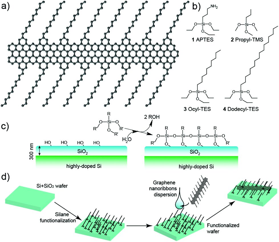 | ||
| Fig. 1 (a) Molecular structure of the graphene nanoribbons. The ribbon structure is repeated regularly all over the length, with only a length distribution being present. (b) Chemical structures of the silanes used for the surface functionalization: 1, (3-aminopropyl)triethoxysilane, APTES; 2, propyl-trimethoxysilane, Propyl-TMS; 3, octyl-triethoxysilane, Octyl-TES; 4, dodecyl-triethoxysilane, Dodecyl-TES. (c) Scheme of the silane monolayer formation in the silanization reaction of SiO2. (d) Scheme of the functionalization process. The wafer is first covered with functional silanes to alter the reaction properties, and then functionalized by drop casting using a dispersion of the molecular GNRs. | ||
In order to exploit the hydrophobicity of the GNRs for the deposition process, we functionalized the surfaces using different silanes (Fig. 1b): (3-aminopropyl)triethoxysilane (APTES), propyl-trimethoxysilane (Propyl-TMS), octyl-triethoxysilane (Ocyl-TES) and dodecyl-triethoxysilane (Dodecyl-TES). These four silanes promote, to a different degree, the deposition of hydrophobic materials via van der Waals interactions. Comparison is also performed with bare Si/SiO2 wafer surfaces, which are terminated by using hydrophilic –OH groups. The silanization (Fig. 1c) was carried out by the insertion of the wafer for 10 s in an aqueous dispersion of the silane, followed by cleaning in isopropanol. The GNRs were then deposited by casting 10 μl drops of a dispersion into N-methyl-2-pyrrolidone12 onto the substrates (Fig. 1d).
The resulting depositions were investigated using atomic force microscopy (AFM) in tapping mode (0.4 Hz, Olympus-3072 tips), as shown in Fig. 2a. Under the employed deposition conditions, only a very few GNRs attach to the bare, untreated Si/SiO2 surface, whereas numerous well-isolated ribbons can be observed on the treated surfaces. The ribbons, although barely visible in the height topography, show an evident contrast in the phase and amplitude signals (Fig. 2b and c), and always appear well-isolated. Even for exceptionally long ribbon lengths (see discussion below), the GNRs appear straight, in sharp contrast to the typical behaviour of carbon nanotubes, which have a strong tendency to coil and bundle on the surface. This behaviour is surprising, as theory predicts that GNRs are more flexible than carbon nanotubes18,19 and also contrasts with observations on top-down GNRs.20,21 One possible explanation lies in a very pronounced interaction between the alkyl side chains of the GNRs and the functionalised surfaces, hindering folding and rolling up of the GNRs.
 | ||
| Fig. 2 (a) AFM amplitude images of the deposited molecular nanoribbons on surfaces functionalised with the different silanes. No ribbons were detected on bare wafer surfaces. (b) Small-area AFM topography of a ribbon deposited on Dodecyl-TMS, showing the details of the height profile. (c) AFM phase signal of a nanoribbon on the Dodecyl-TMS surface, showing the large phase contrast linked to the organic nature of the ribbon and its soft attachment to the surface. | ||
The AFM heights of most ribbons deposited on the functionalised surfaces are found to be around 7 Å (Fig. 3a), in close agreement with the well-established AFM height of monolayer graphene flakes on wafer surfaces.22 The height of monolayer graphene derives largely from adsorbed water and hydrocarbons, and from chemical considerations, one could expect that the nanoribbons do not differ too much in their capacity of adsorbing such species, both above and below the ribbon. This agreement shows that the ribbons are not stacked one onto another, which may be a major issue with synthetically-obtained graphene analogues. The surface deposition of the ribbons thus meets all requirements for the fabrication of single-ribbon electronic nanodevices. The GNR widths are always found to be perfectly homogeneous, and correspond to the lateral AFM resolution, 7 nm, given by the AFM tip radius.
 | ||
| Fig. 3 (a) AFM height profile of a typical molecular nanoribbon, testifying the presence of only one graphitic layer; (b) statistical analysis of the nanoribbon lengths observed with AFM, in dependence of the different surface functionalisation type. Lines are fits with a bimodal distribution (see text); (c) size-exclusion chromatogram of the GNR precursor, after the Diels–Alder polymerisation and pre-graphitisation, showing the bimodal product distribution (eluent: THF; 1 mL min−1; UV detector). | ||
The GNR lengths were found to be similar in all samples, independent of the surface functionalization. For all different functionalisations, a bimodal Gaussian distribution of lengths is always observed, with peaks at 400 ± 20 and 620 ± 20 nm (Fig. 3b). This distribution matches the occurrence of two peaks in size-exclusion chromatography (SEC) analysis,12 performed on the polyphenylene precursor of the same GNR samples employed in this study. The two peaks at different SEC retention times (Fig. 3c) correspond, according to polystyrene standard calibration, to polymeric systems with masses of 360 ± 100 kg mol−1 and 1000 ± 250 kg mol−1, where errors indicate the peak full-width-half-maxima. Such masses would indicate that GNRs made up of 510 ± 120 and 1200 ± 300 repeating units, which provide lengths of 350 ± 100 and 900 ± 250 nm, in reasonable agreement with the AFM distribution. The slight discrepancies between AFM and SEC analyses can be attributed to both the varying absorbances of the different polymer fractions in SEC (larger polymers have higher absorbance per polymer), along with the lower dispersibility and higher susceptibility to aggregation of longer GNRs. Our analysis thus confirms the formation of two preferential lengths, in the synthetic process,11 and excludes the creation of graphene nano-rings via head-to-tail cycloaddition during the polymerisation step. In previous discussions, such rings were considered12 as a plausible synthetic co-product.
While the ribbon length does not vary appreciably with surface functionalization, the surface density δs, given as the number of ribbons per square micron, changes considerably depending on the silane used. The distribution of the occurrence probability Pδs of the GNR densities were analysed with the quadrat method,23,24 choosing surface bins of 400 μm2 (Fig. 4a). The distributions show that an increasingly hydrophobic character of the surface results in a marked increase in the number of area units with larger δs. While no area unit has more than 2 GNRs for the bare SiO2 surface, the Dodecyl-TES functionalization leads to 30% probability of having δs > 3, with ca. 4% of the area units displaying up to 6 GNRs. The quadrat analysis also allows a rough assessment of the deposition process24via the parameter ζ = Vδ/m (with Vδ the statistical variance in δs and m the mean value), which should be 1 for a random deposition, 0 for a regular arrangement and ≫1 for clustered GNRs. The ζ values fall in the 1.2–1.6 range for all depositions, indicating slight clustering effects that become more pronounced on increasing the hydrophobic character of the surface (ζ = 1.6 in Dodecyl-TES). This weak tendency toward clustering, detectable also in the distributions of Pδs by the large remnant weight at δs = 0, is attributable to small surface defects and bumps, which help in local retention of the GNRs.
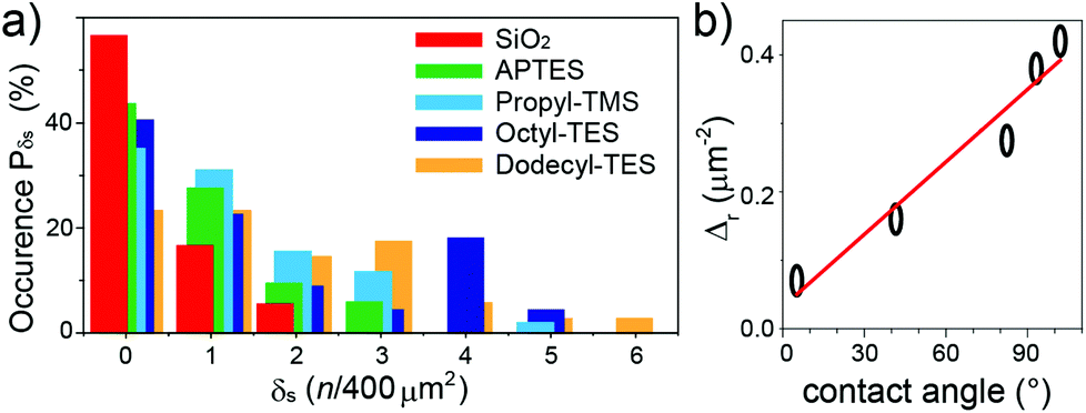 | ||
| Fig. 4 (a) Statistical distribution of the surface ribbon density, obtained from quadrat analysis of the differently-functionalized surfaces (see legend). The bars are slightly shifted horizontally to better show the evolution of the distributions. (b) Dependence of the surface ribbon density Δr on the surface hydrophobicity, measured as the water contact angle. Dot sizes correspond to estimated errors. | ||
The importance of the surface-anchored groups is immediately detectable when considering the overall surface density  , against the water contact angle, which is known from the literature and offers a good measure of the surface hydrophobicity. A clear correlation trend is observed (Fig. 4b), when the length of the alkyl chain attached to the silane is increased, leading to a higher hydrophobicity of the surface. This non-covalent chemistry can already provide a more than four-fold enhancement of Δr from bare SiO2 to the longest alkyl chain (Dodecyl-TES). The dependency is much stronger than for carbon nanotube depositions,25 and likely due to the decisive interaction with the ribbon's dodecyl-side-chains.
Furthermore, we investigated the deposited ribbons using micro-Raman spectroscopy, which is one of the main tools for graphene characterization.26–29 Graphene Raman spectra excited at 488 nm are characterized by a 2D peak around 2700 cm−1 and a G peak at 1585 cm−1, plus additional D and D′ peaks that correspond to Raman-forbidden transitions, in a perfect graphene layer, and become activated by single-phonon inter-valley and intra-valley scattering processes, respectively. In GNRs the activation mechanisms are still unclear and await complete theoretical investigation, so that we only use the graphene peak labelling by analogy. Micro-Raman spectra of individual GNRs (Fig. 5) clearly show all the aforementioned peaks, plus the D + D’, G + D and 2D′ overtone features, enabling precise peak determination even for slightly-overlapping G and D′ peaks. G and 2D peaks are found at 1610 and 2675 cm−1, respectively, and the deviations from graphene values can be attributed to lateral confinement effects,12 which are also responsible for the pronounced D and D′ peaks appearing at 1348 and 1621 cm−1, respectively.12,30 The Raman spectra acquired on the liquid dispersions of the ribbons display the same features, with very similar relative intensities of the peaks, but considerable peak broadening and a 13 cm−1 downshift of the D peak are present, possibly linked to partial stacking in the dispersions.26–29 The peaks of the ribbons in dispersion, in contrast to those of the deposited ribbons, could not be fitted with single Lorentzian lineshapes, but with Gaussian lines, indicating inhomogeneous broadening by sample averaging.31 By comparison, the Raman spectrum of non-molecular ribbons (obtained by etching a 100 nm wide patch from a single-layer exfoliated graphene flake via e-beam negative resist lithography) displays dominant D and 2D peaks, as well as D′ and 2D′ peaks whose intensity is only a fraction of the those of the GNRs.
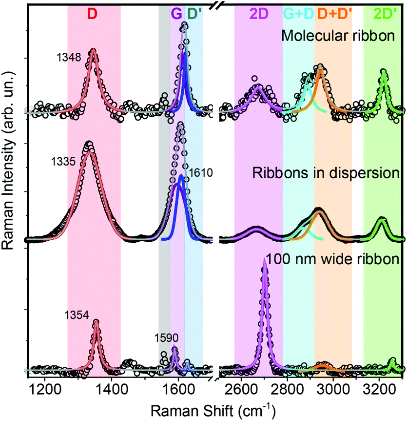 | ||
| Fig. 5 Raman spectrum of an individual GNR on the Dodecyl-TES-functionalised surface (top) compared to the spectrum of a drop of the GNR in dispersion (middle) and to that of a 100 nm wide ribbon etched from exfoliated graphene by oxygen-plasma treatment (bottom). The lines are fits to the data (see text) while the colour bars highlight the different spectral regions. | ||
Conclusions
We have demonstrated that the silanization of Si/SiO2 surfaces allows tuning the deposition of molecular graphene nanoribbon with atomically-precise edges. This opens up the possibility to fabricate large numbers of GNR-based nanoelectronic devices in parallel. Moreover, it enables a detailed statistical analysis of the ribbon structure, which is useful to identify strategies to further improve the synthesis protocol. Our analysis of the surface densities reveals that the deposition is influenced by van der Waals interactions between the ribbons and the functionalized surface. GNR deposition differs remarkably from that of carbon nanotubes, for both the folding and the effect of the surface functionalization. The observations also shed new light on the nature of the synthetic products, and will prompt a better understanding of the chemical processes. Raman spectra of deposited ribbons show fingerprint features, not present in etched ribbons, which are promising to identify molecular ribbons. These findings pave the way to the detailed study of single molecular GNR and their use in nanoelectronics, and offer exciting perspectives for graphene spintronics.27,32,33Acknowledgements
We thank C. Casiraghi for insightful discussions and acknowledge financial support from German DFG, the BW-Stiftung (Kompetenznetz Funktionelle Nanostrukturen), the Royal Society via the University Research Fellowship, the AvH Stiftung (Sofja Kovalevskaja award), the IMPRS-AM and EU via the grants ERC-StG-338258-“OptoQMol”, ERC-AdG-“NANOGRAPH”, MoQuaS FP7-ICT-2013-10 and the EU Graphene Flagship (no. CNECT-ICT-604391).References
- A. H. Castro Neto, F. Guinea, N. M. R. Peres, K. S. Novoselov and A. K. Geim, Rev. Mod. Phys., 2009, 81, 109 CrossRef CAS.
- A. K. Geim and K. S. Novoselov, Nat. Mater., 2007, 6, 183–191 CrossRef CAS PubMed.
- F. Bonaccorso, Z. Sun, T. Hasan and A. C. Ferrari, Nat. Photonics, 2010, 4, 611 CrossRef CAS.
- W. Yang, K. R. Ratinac, S. P. Ringer, P. Thordarson, J. J. Gooding and F. Braet, Angew. Chem., Int. Ed., 2010, 49, 2114 CrossRef CAS PubMed.
- N. Tombros, C. Jozsa, M. Popinciuc, H. T. Jonkman and B. J. van Wees, Nature, 2007, 448, 571 CrossRef CAS PubMed.
- P. Avouris, Z. Chen and V. Perebeinos, Nat. Nanotechnol., 2007, 2, 605–615 CrossRef CAS PubMed.
- O. V. Yazyev, Rep. Prog. Phys., 2010, 73, 056501 CrossRef.
- Y. Wang, A. Vallabhaneni, J. Hu, B. Qiu, Y. P. Chen and X. Ruan, Nano Lett., 2014, 14, 592–596 CrossRef CAS PubMed.
- J. Hu, X. Ruan and Y. P. Chen, Nano Lett., 2009, 9, 2730–2735 CrossRef CAS PubMed.
- B. Trauzettel, D. V. Bulaev, D. Loss and G. Burkard, Nat. Phys., 2007, 3, 192–196 CrossRef CAS.
- J. cai, P. Ruffieux, R. Jaafar, M. Bieri, T. Braun, S. Blankenburg, M. Muoth, A. P. Seitsonen, M. Saleh, X. Feng, K. Müllen and R. Fasel, Nature, 2010, 466, 470–473 CrossRef CAS PubMed.
- A. Narita, X. Feng, Y. Hernandez, S. A. Jensen, M. Bonn, H. Yang, I. A. Verzhbitskiy, C. Casiraghi, M. R. Hansen, A. Koch, G. Fytas, O. Ivasenko, B. Li, K. Mali, T. Balandina, S. Mahesh, S. De Feyter and K. Müllen, Nat. Chem., 2014, 6, 126–132 CrossRef CAS PubMed.
- A. N. Abbas, G. Liu, A. Narita, M. Orosco, X. Feng, K. Müllen and C. Zhou, J. Am. Chem. Soc., 2014, 136, 7555–7558 CrossRef CAS PubMed.
- T. H. Vo, M. Shekhirev, D. A. Kunkel, M. D. Morton, E. Berglund, L. Kong, P. M. Wilson, P. A. Dowben, A. Enders and A. Sinitskii, Nat. Commun., 2014, 5, 3189 Search PubMed.
- N. Abdurakhmanova, N. Amsharow, S. Stepanow, M. Jansen, K. Kern and K. Amsharov, Carbon, 2014, 77, 1187 CrossRef CAS.
- P. B. Bennett, Z. Pedramrazi, A. Madani, Y.-C. Chen, D. G. de Oteyza, C. Chen, F. R. Fischer, M. F. Crommie and J. Bokor, Appl. Phys. Lett., 2013, 103, 253114 CrossRef.
- D. Janssen, R. De Palma, S. Verlaak, P. Heremans and W. Dehaen, Thin Solid Films, 2006, 515, 1433–1438 CrossRef CAS.
- H. Pan and B. Chen, Sci. Rep., 2014, 4, 4198 Search PubMed.
- K. Bets and B. Yakobson, Nano Res., 2009, 2, 161 CrossRef CAS.
- X. Li, X. Wang, L. Zhang, S. Lee and H. Dai, Science, 2008, 319, 1229 CrossRef CAS PubMed.
- L. Jiao, L. Zhang, X. Wang, G. Diankov and H. Dai, Nature, 2009, 458, 877 CrossRef CAS PubMed.
- K. S. Novoselov, D. Jiang, F. Schedin, T. J. Booth, V. V. Khotkevich, S. V. Morozov and A. K. Geim, Proc. Natl. Acad. Sci. U. S. A., 2005, 102, 10451–10453 CrossRef CAS PubMed.
- B. D. Ripley, Spatial Statistics, J. Wiley and Sons, Hoboken, New Jersey, 2nd edn, 2004 Search PubMed.
- H. Solomon, Geometric Probability, SIAM, Philadelphia, 1978 Search PubMed.
- K. H. Choi, J. P. Bourgoin, S. Auvray, D. Esteve, G. S. Duesberg, S. Roth and M. Burghard, Surf. Sci., 2000, 462, 195–202 CrossRef CAS , and references therein.
- A. C. Ferrari and D. M. Basko, Nat. Nanotechnol., 2013, 8, 235–246 CrossRef CAS PubMed.
- M. S. Dresselhaus, A. Jorio and R. Saito, Annu. Rev. Condens. Matter Phys., 2010, 1, 89–108 CrossRef CAS.
- A. C. Ferrari, J. C. Meyer, V. Scardaci, C. Casiraghi, M. Lazzeri, F. Mauri, S. Piscanec, D. Jiang, K. S. Novoselov, S. Roth and A. K. Geim, Phys. Rev. Lett., 2006, 97, 187401 CrossRef CAS PubMed.
- C. Casiraghi, S. Pisana, K. S. Novoselov, A. K. Geim and A. C. Ferrari, Appl. Phys. Lett., 2007, 91, 233108 CrossRef.
- S. Ryu, J. Maultzsch, M. Y. Han, P. Kim and L. E. Brus, ACS Nano, 2011, 5, 4123–4130 CrossRef CAS PubMed.
- P. G. Etchegoin and E. C. Le Ru, Anal. Chem., 2010, 82, 2888–2892 CrossRef CAS PubMed.
- C. Cervetti, E. Heintze and L. Bogani, Dalton Trans., 2014, 43, 4220–4232 RSC.
- C. Cervetti, E. Heintze, B. Gorshunov, E. Zhukova, S. Lobanov, A. Hoyer, M. Burghard, K. Kern, M. Dressel and L. Bogani, Adv. Mater., 2015, 27, 2676 CrossRef.
| This journal is © The Royal Society of Chemistry 2015 |