
 Open Access Article
 This Open Access Article is licensed under a Creative Commons Attribution-Non Commercial 3.0 Unported Licence
Spontaneous doping of two-dimensional NaCl films with Cr atoms: aggregation and electronic structure†
Zhe
Li
a,
Hsin-Yi Tiffany
Chen
b,
Koen
Schouteden
a,
Ewald
Janssens
a,
Chris
Van Haesendonck
a,
Peter
Lievens
*a and
Gianfranco
Pacchioni
*b
aLaboratory of Solid-State Physics and Magnetism, KU Leuven, Celestijnenlaan 200d – box 2414, B-3001 Leuven, Belgium. E-mail: peter.lievens@fys.kuleuven.be
bDipartimento di Scienza dei Materiali, Università di Milano-Bicocca, Via Cozzi 55, I-20125 Milano, Italy. E-mail: gianfranco.pacchioni@mater.unimib.it
First published on 18th December 2014
Abstract
Scanning tunneling microscopy (STM) experiments combined with density functional theory (DFT) calculations reveal that deposited Cr atoms replace either Na or Cl ions, forming substituting dopants in ultrathin NaCl/Au(111) films. The Cr dopants exchange electrons with the support thus changing the electronic properties of the film and in particular the work function. The Cr atoms spontaneously aggregate near the edges of the bilayer (2L) NaCl islands, forming a new phase in the insulator with a remarkably dense population of Cr dopants. The spectra of differential conductance yield evidence that, compared to the undoped or Cr-poor 2L NaCl films on Au(111), the Cr-rich region shows different interface states, shifted image-potential states, and a reduced work function. This demonstrates the potential of doping ultrathin films to modify their adsorption properties in a desired manner.
1. Introduction
Introducing magnetic metal atoms and their aggregates into non-magnetic surfaces allows one to synthesize novel materials for magneto-optical, spintronic, and data-storage devices.1–3 Thin insulating films provide the possibility to control the electronic coupling between magnetic metal nanostructures and the conducting substrate. The magnetic atoms can be either adsorbed on top of the surfaces or, more rarely, can be incorporated into the insulating films, which may lead to novel functionalities, such as the formation of a new doping-induced phase,4 the modification of adsorption and surface chemical properties,5 or ferromagnetic insulators.6,7The electronic and magnetic properties of the deposited magnetic metal atoms are very sensitive to their local environment that determines system symmetry and state hybridizations.8–11 Scanning tunneling microscopy (STM) and scanning tunneling spectroscopy (STS) have been used to investigate at the atomic scale the main mechanisms that are at the origin of their unique properties, such as charge transfer,5 magnetic stability, and coupling.3 For example, Rau et al. recently demonstrated that the magnetic anisotropy energy of a 3d transition metal atom can reach its maximum value on MgO thin films,12 while the anisotropy is typically much smaller on other surfaces.8 So far, magnetic atoms have been mainly investigated on Cu2N and MgO films.8,12 Ultrathin NaCl films represent an alternative and appealing insulating material due to the large band gap of NaCl and because the thickness of the films can be controlled with monolayer precision, giving rise to truly two-dimensional (2D) systems. To date, mainly non-magnetic atoms13,14 and molecules15–19 have been investigated on ultrathin NaCl insulating films. It has been found that the Au and Ag atoms are weakly bound on top of the NaCl surface. Very recently we reported an uncommon example of spontaneous doping of NaCl films by magnetic Co atoms.20
In this paper, we investigate the behavior of Cr atoms deposited on bilayer (2L) NaCl/Au(111) films. While the tendency of the Cr atoms to spontaneously enter into the film is similar to what we found for Co,20 the electronic structure of the Cr-doped NaCl films and the distribution of these transition metal impurities is very different from the Co case. By comparing the results for our experimental STM/STS data and our density functional calculations, we find that there is an electron exchange of the Cr dopants with the Au support, which changes the electronic properties of the film. A remarkable spontaneous aggregation of Cr dopants occurs near the edges of the 2L NaCl islands, forming an amorphous structure that exhibits different interface states and image-potential states (IPSs) compared to the undoped and Cr-poor NaCl films. The observed shift of the IPSs is related to a modified work function, resulting from the surface dipole created by electron transfer from a dense population of Cr dopants towards the Au support. These effects, which were not observed for Co adsorption, show that there is great potential in the deposition of transition metal atoms on NaCl ultrathin films as this can result in new materials with distinct and interesting properties. These properties can be tuned by an appropriate choice of the self-doping element.
2. Methods
2.1. Experimental details
Monolayer (1L) and 2L NaCl(100) islands on Au(111) are obtained by the deposition of NaCl (99.999% purity, Alfa Aesar), which is heated up to 800 K, on a cold [well below room temperature (RT)] Au(111) surface as described in ref. 21. Trilayer (3L) NaCl is obtained by mild post-annealing to about 470 K.22 Cr atoms are thermally evaporated onto the NaCl/Au(111) substrate that is kept at RT. (dI/dV)(V) curves and maps of the local density of states (LDOS) are acquired with an open and closed feedback loop, respectively, by lock-in detection using amplitudes of 50 mV and frequencies around 880 Hz. All STM measurements are performed at 4.5 K using a tungsten tip in an ultra-high vacuum system that includes a low-temperature STM (Oxford Instruments – Omicron NanoScience). Image processing is performed by Nanotec WSxM.232.2. Computational details
Spin-polarized DFT calculations were performed using the generalized gradient approximation (PBE functional24) and the plane wave code VASP.25,26 The interaction between the ions and the valence electrons is described by the projector augmented wave (PAW) method.27 The NaCl(100) films on the Au(111) substrate have been modelled by a coincidence structure, obtained by superposing a (2 × 2) NaCl(100) unit cell on a superstructure of the Au(111) surface.28 This coincidence structure presents a residual strain of about 5%, which is accommodated in the Au substrate; the angle of the substrate unit cell is adjusted from 82° to 90° to match the square symmetry of the NaCl film. The metal support is modelled by a five layer slab. A (6 × 6 × 1) Monkhorst–Pack grid is used for reciprocal space sampling.
For the electronic properties and STM image simulations of substitutional Cr impurities, (2 × 2) and (4 × 4) NaCl(100) supercells were used, corresponding to 12.5% and 3.1% atomic concentration doping of the top layer. For (2 × 2) supercells, the atomic coordinates of the top three layers of the Au slab and all coordinates of the NaCl films and Cr are fully relaxed. For the larger (4 × 4) unit cell all the coordinates of the Au support were fixed, a procedure that does not affect the properties.
Dispersion interactions were included by means of the pair-wise force field as implemented by Grimme (DFT-D2).29 STM images were simulated using the Tersoff–Hamann approximation.30 The reported magnetic moments are the total magnetic moments per unit cell.
3. Results and discussion
3.1. Charge transfer between individual Cr dopants in 2L NaCl and the Au(111) support
Upon deposition of Cr atoms onto 2L [Fig. 1(a)], the Cr atoms are found to be located either on Cl sites, which are hereafter referred to as CrCl [brighter protrusions indicated by white arrows in Fig. 1(b) and (c)], or on Na sites, hereafter referred to as CrNa [less bright protrusions indicated by black arrows in Fig. 1(b) and (c)]. Note that with a bare (i.e., non-functionalized) metallic tip, only the Cl ions of the NaCl lattice can be revealed as protrusions.31 The corrugation stemming from the Cl ions is about 2.5 pm in the STM topography image in Fig. 1(b). Within the tunneling voltage range from −1 to +1 V, the CrCl atoms have an apparent height around 30 pm, while the CrNa atoms have an apparent height around 10 pm. We will show below that the Cr atoms enter into the NaCl film as substitutional dopants, replacing the Cl and Na ions. | ||
| Fig. 1 (a) 53 × 44 nm2 STM topography image (V = 1 V, I = 0.05 nA) of Cr atoms on 2L NaCl/Au(111). (b) 15 × 15 nm2 STM topography image (V = 1 V, I = 0.05 nA) taken in the center of the NaCl island in (a). (c) 15 × 15 nm2 atomic-resolution STM topography image (V = 1 V, I = 0.05 nA) taken near the edge of another 2L NaCl island. The obviously brighter protrusions indicated by white arrows are CrCl atoms, while the weaker protrusions indicated by black arrows are CrNa atoms. (d)–(f) 2.8 × 4.8 nm2 STM topography images of a CrCl atom and a CrNa atom taken at +2.0 V, +2.4 V, and +3.1 V, respectively. (g) dI/dV spectra recorded at CrCl, CrNa and the surrounding NaCl. | ||
Fig. 1(d)–(g) present a series of STM topography images and dI/dV spectra of CrNa and CrCl atoms. Within the measured energy range indicated in Fig. 1(g), CrNa atoms exhibit four unoccupied states around 2.0, 2.4, 3.1, and 4.0 eV, while CrCl atoms exhibit only one pronounced resonance state around 3.9 eV. Note that for the undoped 2L NaCl film there are two resonances at 3.75 eV (shoulder peak) and 4.25 eV (main peak), which are related to the Au bulk band gap edge32 and the first image potential state of the 2L NaCl film,33 respectively. The conduction band may be mixed in the IPSs.34 At voltages near the Cr resonance states, CrNa atoms appear as sphere-shaped protrusions around 2.0 eV [Fig. 1(d)] and 2.4 eV [Fig. 1(e)] and as a four-lobe structure around 3.1 eV [Fig. 1(f)] in the STM topography images, while CrCl atoms simply appear more pronounced with increasing voltage within the entire investigated voltage range up to 3.1 eV [Fig. 1(d)–(f)]. The extended four-lobe structure is indicative of the hybridization between the orbitals of the Cr atom and its neighboring Cl ions, as follows from our DFT-based calculations discussed below. Note that we did not observe any Kondo signature near the Fermi level. Since there is one layer of NaCl between the Cr dopant and the Au surface, the Kondo effect is expected to be very weak and the Kondo temperature may be below our experimental temperature (4.5 K).
DFT calculations were performed for a Cr atom replacing either a Na or a Cl ion in the top layer of a 2L NaCl film. 2 × 2 and 4 × 4 supercells were used, representing 12.5% and 3.1% Cr doping concentrations of the top layer of the NaCl film, respectively. The replaced Na or Cl atoms are not considered in the models because it is assumed that they are either displaced to the borders of the islands or to the NaCl/Au interface.35
When Cr replaces one Na+ ion in a free-standing, unsupported 2L NaCl film, it assumes a +1 formal charge (Bader charge = +0.81|e|). The electronic configuration becomes 4s03d5 (4s13d5 for the free Cr atom) and the magnetization is 5μB (five 3dα electrons) [see Fig. S3 in ESI†]. In a symmetric way, when Cr replaces one Cl− ion in the unsupported NaCl 2L film it assumes a −1 formal charge (Bader charge = −0.60|e|) and the electronic configuration becomes 4s23d5 (magnetization 5μB, as for CrNa).
The electronic structure becomes, however, very different for the supported 2L NaCl films on Au(111). Here in fact, an electron exchange between the transition metal impurity and the Au support is possible, giving rise to different oxidation states. Similar phenomena have been described recently for the case of Cr and Mo impurities in MgO and CaO surfaces.5,20,35–37 Our calculations for CrNa/NaCl(2L)/Au(111) show that the ground state corresponds to a Cr ion with four 3d electrons, i.e., the 4s03d4 configuration [see Fig. S4 in ESI†]. The Cr is thus formally in a +2 oxidation state and has donated one electron to the supporting Au metal. The net magnetization is 3.87μB and the Bader charge is +1.27|e| (see Table 1).
| Doping | Nα–Nβ (μB) | q |e| | Φ, calc. (eV) | Φ, exp. (eV) | |
|---|---|---|---|---|---|
| a Cr-rich regions, containing mainly CrCl, but also a fraction of CrNa. b Cr-poor regions, containing mainly CrNa, but also a fraction of CrCl. c Taken from ref. 44. | |||||
| CrNa/NaCl/Au(111) | 12.5% | 4.06 | +1.19 | 3.56 | |
| CrCl/NaCl/Au(111) | 12.5% | 5.64 | −0.23 | 3.42 | |
| Cr/NaCl/Au(111) | ≈6% | 3.8a | |||
| CrNa/NaCl/Au(111) | 3.1% | 3.87 | +1.27 | 4.03 | |
| CrCl/NaCl/Au(111) | 3.1% | 5.98 | −0.09 | 3.43 | |
| Cr/NaCl/Au(111) | ≈1% | 4.3b | |||
| NaCl/Au(111) | — | — | — | 4.40 | 4.3 |
| Au(111) | — | — | — | 5.13 | 5.36c |
We now consider the CrCl case. From a structural point of view, when Cr replaces Cl it is calculated to protrude by about 0.19 pm from the surface [Fig. 2(b)]. This Cr protrusion is found on unsupported as well as on supported NaCl 2L films. The fact that CrCl atoms are more protrusive than CrNa is consistent with the experimental observations. This may indicate the existence of a residual strain in the NaCl film, a fact consistent with the experimental observation that CrCl atoms are preferentially found at the edges of NaCl islands, where the strain can be partially released. We performed a set of calculations where Cr is forced to stay in the topmost NaCl layer (no protrusion, Fig. S5 in ESI†) but the main electronic features do not change. As for CrNa, and also for CrCl there occurs an electron exchange between the Cr dopant and Au. The electronic configuration of CrCl is 4s13d5 (the same as that for a free Cr atom). Compared to the unsupported NaCl film (where Cr adopts a Cr− 4s23d5 configuration), the Cr 4sβ orbital in 2L NaCl/Au(111) films is pushed above the Au Fermi level and is empty [see Fig. S5 in ESI†]. The net magnetization is 5.98μB and the Bader charge is close to 0|e| (see Table 1), indicating that one electron has been transferred to the supporting Au metal, and that the Cr atom is almost neutral (instead of being Cr− as in the unsupported 2L NaCl).
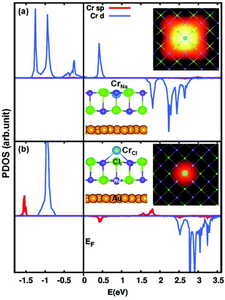 | ||
| Fig. 2 Projected density of states (PDOS) of 2L NaCl/Au(111) films with Cr substituting Na (a) and Cl (b), respectively. See Fig. S4 and S5 in ESI† for the decomposition of Cr 3d and 4sp orbitals. Structures and simulated STM images are presented in the insets. | ||
We now discuss the positions of the empty states for the CrNa and CrCl dopant atoms. An analysis of the density of states indicates that the CrNa empty 3d states give rise to four separate peaks [around 1.8, 2.2, 2.4, and 2.7 eV, see Fig. 2(a)], which is in good agreement with the experimental STS spectra [Fig. 1(g)]. We note that in DFT the calculated energy levels appear at lower energies when compared to the experiment. This is because at the DFT-GGA level the band gap of NaCl is underestimated, also affecting the position of the defect states in the gap.
Direct evidence for the unoccupied 3d orbitals for CrNa comes from the simulated STM topography images, as presented in Fig. 2. A four lobe structure is clearly visible and can be attributed to the hybridization of the Cr 3dxy (1.8 eV), 3dxz + 3dyz (2.2 eV), and 3dx2–y2 (2.4 eV) empty states with the Cl 3p orbitals [also see the projected density of state (PDOS) curves in Fig. S4(b) in ESI†].
The empty states for CrCl lie in the region from 2.4 to 3.4 eV [see Fig. 2(b)]. Most relevantly, the main peaks for CrCl are at higher energies compared to CrNa. The CrCl lowest feature, at 2.5 eV, is slightly below the CrNa highest peak at 2.7 eV. This is consistent with what is found experimentally in the dI/dV spectra for CrCl, showing the first peak at 3.9 eV while the highest CrNa feature is at 4.0 eV [see Fig. 1(g)].
For CrCl two sets of simulated STM images were obtained, corresponding to a Cr protruding from the surface and to a Cr ion within the NaCl top layer. In both cases a round bright featureless image is observed [see Fig. S5 in ESI†]. Note that only one of the four empty states for CrCl [see Fig. 2(b)] can be revealed in the experimental dI/dV spectra [see Fig. 1(g)], while the other states are above the experimentally accessible energy range for stable STM/STS measurements. At higher voltages, either the Cr atoms may be removed, or the STS may be dominated by the conduction band and image states of the NaCl film.
The good agreement between experimental dI/dV spectra and calculated PDOS, as well as between measured and simulated STM images, provides solid proof that the Cr atoms substitute either Na or Cl ions in the top layer of the NaCl film, and that there occurs a charge transfer from the Cr dopants to the Au substrate.
In earlier work we demonstrated that Co atoms can also substitute both Na and Cl ions in the top layer of a NaCl film.20 Despite this similarity, the electronic properties of Cr dopants are very different from those of Co dopants. In particular, the Cr dopants give rise to an electron transfer towards the metal substrate, which is a typical example of change in the charge state of a dopant in insulating films due to the presence of the support. No such charge transfer was found for Co dopants. The Co dopants simply take the charge of the Na and Cl atoms they replace.20 The occurrence of a charge transfer from the Cr dopant to the Au(111) support is also evidenced by the observed work function change of the NaCl/Au(111) film for high concentrations of Cr dopants, as described in the next section.
3.2. Spontaneous aggregation of Cr dopants in 2L NaCl films
When Co atoms are deposited onto 2L NaCl, the two types of substitutional doping (CoNa and CoCl) are randomly distributed across the surface.20 In the present work, the Cr dopant atoms show a very different and more interesting behavior: many Cr atoms are retrieved near the edge of the 2L NaCl islands, as illustrated in Fig. 1(a). One possible reason may be that the NaCl film reorganizes after Cr deposition and therefore the Cr atoms move towards the edges. Atomic-resolution images reveal that in the middle of the NaCl islands there are almost no CrCl atoms, while there are many CrNa atoms [Fig. 1(b)]. Near the edges of the NaCl islands there are clearly many more CrCl atoms [Fig. 1(c)]. The undoped (i.e., before the Cr deposition) 2L NaCl islands are typically nearly perfect squares on metal surfaces33 [also see Fig. S1(a) in ESI†]. Remarkably, upon Cr deposition, the corners of the square become truncated [Fig. 1(a)]. This implies significant reorganization of the NaCl film and is indicative of the Cr-induced formation of a new phase.After deposition of more Cr atoms, the Cr-rich edge regions of the 2L NaCl film become larger, while the center of the islands contains almost no CrCl atoms, yet plenty of CrNa atoms (Fig. 3). It can be clearly seen from the LDOS maps [Fig. 3(b) and (c)] that the edges of the NaCl islands exhibit an LDOS pattern similar to that of Au(111), while the center region of the NaCl islands has an LDOS pattern that is obviously different from the surrounding. As can be observed in Fig. 3(b)–(d), there is a marked boundary between the two regions. In Fig. 3(d), the upper region is Cr-poor (mainly CrNa) doped NaCl with a doping concentration (atomic percentage of Cr atoms incorporated into the top layer of the NaCl film) of about 1.4%, while the lower region is Cr-rich (mainly CrCl) doped NaCl with a higher doping concentration of about 6%. We emphasize that the Cr rich regions always have a more or less constant Cr concentration, regardless of the deposited amount of Cr atoms. Only the size of that area can be changed by depositing less or more Cr atoms. Even with a very low coverage of Cr atoms, at the edge of the island there is still a high density of Cr dopants [see Fig. 1(a) and (c)]. In the Cr-rich region, the Cr atoms retain their individual character, i.e., they do not form metal–metal bonds leading to larger Cr particles. Instead they seem to remain at a certain minimal distance from each other, as if they repel each other (Fig. S2 in the ESI† and the corresponding discussion). Within the accuracy of our experiments, the NaCl lattice is not affected upon Cr deposition.
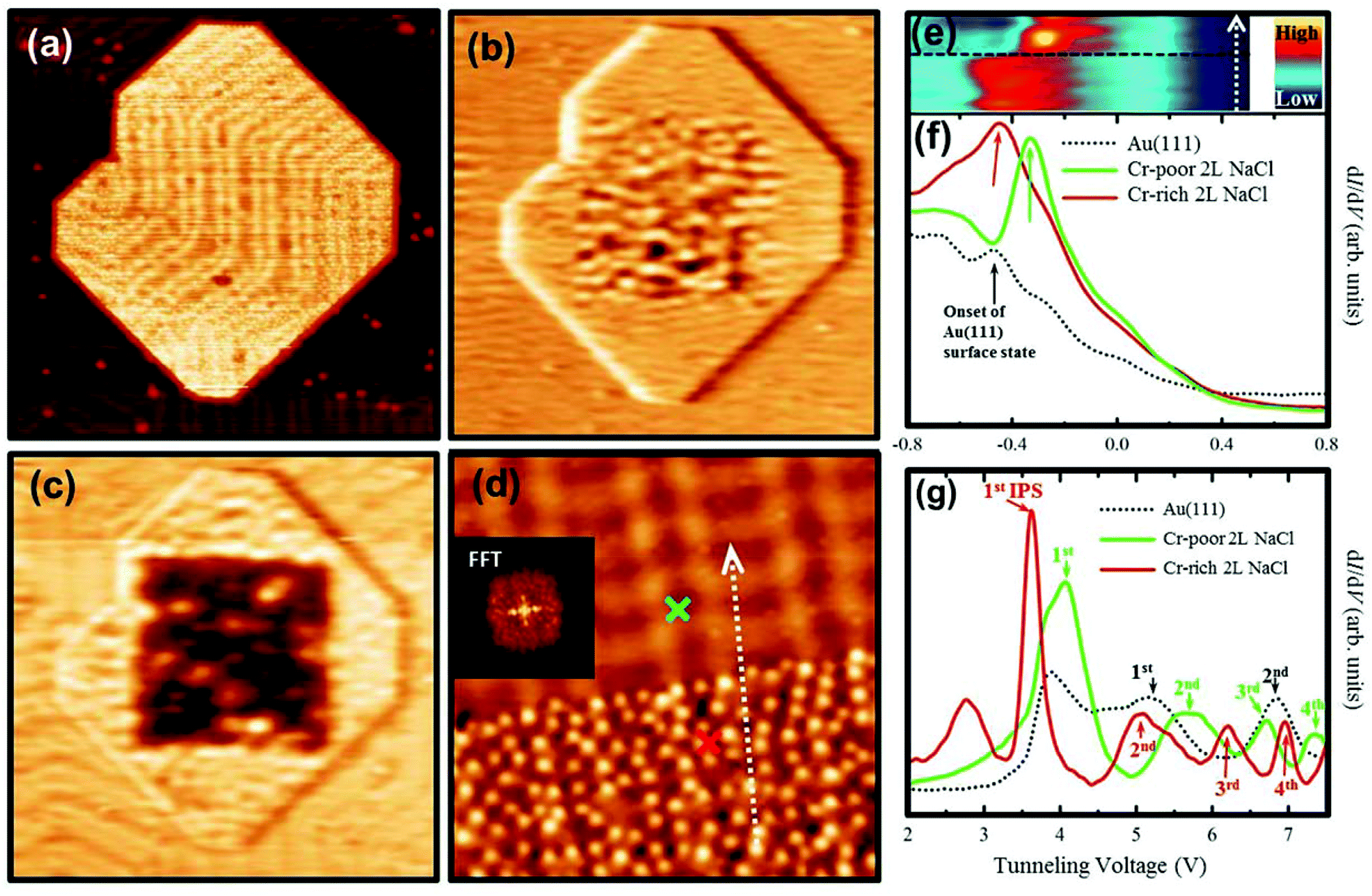 | ||
| Fig. 3 (a) 80 × 80 nm2 STM topography image of Cr atoms on 2L NaCl/Au(111) and the corresponding LDOS maps taken at (b) V = −0.2 V, I = 0.05 nA and (c) V = −0.4 V, I = 0.1 nA. (d) 21 × 21 nm2 STM topography image (V = 0.6 V, I = 0.1 nA) taken near the edge of another 2L NaCl island. The inset is a 4 nm−1 × 4 nm−1 fast Fourier transform (FFT) pattern of the Cr-rich region. (e) 1.3 V × 12 nm color visualization of (dI/dV)(V) spectra taken along the dotted white arrow indicated in (d). The horizontal black dashed line in (e) indicates the boundary between the Cr-rich and Cr poor region. (f) and (g) dI/dV spectra taken on the clean Au(111) surface, the Cr-rich region [near the red cross in (d)], and the Cr-poor region [near the green cross in (d)] of the 2L NaCl island in the −0.8 to 0.8 eV and 2 to 7 eV ranges, respectively. The arrows in (f) mark the onset of the interface state for the Cr-poor and Cr-rich regions. The arrows in (g) mark the positions of the image-potential states (IPSs). | ||
Remarkably, dI/dV spectra in Fig. 3(f), which reflect the surface/interface states, indicate that the onset of the interface state of the Cr-rich region is almost identical to that of the Au(111) surface state. However, this onset of the Cr-rich region differs from that of the Cr-poor region, which is in turn similar to that of the undoped 2L NaCl film.22 The onset energy for the Cr-rich region shifts as much as 200 mV towards lower energy compared to the undoped/Cr-poor region. The 2D visualization of (dI/dV)(V) spectra [Fig. 3(e)] taken along a line [dashed arrow in Fig. 3(d)] that crosses the Cr-rich and Cr-poor regions reveals an abrupt change of the interface states at the border, which excludes the possible effect of the boundary states near the edge of the NaCl islands. The different interface states in Cr-poor and Cr-rich regions can be explained by their different dielectric constants in a phase-accumulation model.38 The reduced dielectric constant induced by a large amount of Cr in the Cr-rich region leads to a shift of the interface states towards lower energy.39
The dI/dV spectra in Fig. 3(g) reveal several unoccupied states that originate from the image-potential states (IPSs). The IPSs for Au(111) are assigned according to previous studies (see, e.g., ref. 32). For Cr-poor 2L NaCl, the positions of the peaks in the spectra are similar to those of the undoped 2L NaCl (data not shown) with respect to Au(111). The IPSs for NaCl on metal surfaces have been shown to appear at lower energies than those for the non-covered metal.32,40 Therefore, the first main peak for Cr-poor 2L NaCl can be assigned as the first IPS. Four IPSs are identified within the measured energy range. Following the recent work reported in ref. 34, the onset of the conduction band of 2L NaCl is likely to be hidden in the IPS resonances. Turning to Cr-rich 2L NaCl, we assign the second peak in the spectra as the first IPS, since for two different surfaces the energy shift between the two series of IPSs should be similar for each of the peaks.32,40–42 Assigning any other peak as the first IPS for the Cr-rich 2L NaCl would result in a significant variation of the energy difference between the corresponding IPSs for the Cr-poor and the Cr-rich surfaces. The first small peak appearing in the spectra taken on Cr-rich 2L NaCl can be assigned as its conduction band gap edge. The observed IPSs on the Cr-rich region appear about 0.5 eV lower than those on the Cr-poor region; the IPSs of the Cr-poor region, in turn, appear on average about 1.1 eV lower than those on the bare Au(111) surface. Since the energy difference of the IPSs between the undoped NaCl film and Au(111) is also about 1.1 eV (data not shown), it turns out that the IPSs of the Cr-poor region are practically indistinguishable from those of the undoped NaCl film. The energy difference of the corresponding IPSs between different surfaces reflects different work functions.33,40,43 Ignoring the possible Stark effect related shifts in the STS and using the experimental Au(111) work function ΦAu of 5.36 eV,44 we estimate ΦCr-rich for the Cr-rich region to be about 3.8 eV. On the other hand, we estimate ΦNaCl for the undoped NaCl/Au(111) 2L film to be 4.3 eV. This then corresponds to a shift ΔΦ = ΦCr-rich − ΦNaCl of −0.5 eV, indicating that the Cr-rich NaCl film is a different phase than the undoped 2L NaCl. Note that the absolute values of the work functions are just an approximation because of the possible Stark shift, but they qualitatively reflect the work function variations between the different regions.
To understand the physical origin of the change in work function, additional DFT calculations were performed. For the Au(111) surface the calculations give a work function of 5.13 eV (5.36 eV in the experiment44). Upon deposition of the NaCl layer there occurs a decrease in the work function, by 0.73 eV in the calculations and by about 1.1 eV in the experiment (see Table 1). This decrease has been reported in other studies as well,33,45 and is due to the compressive effect of the NaCl insulating film on the metal electron density.46,47 When Cr replaces either Na or Cl in the film, the work function decreases further (see Table 1). The computed Φ values for CrNa are 3.56 eV at 12.5% doping concentration and 4.03 eV at 3.1% doping concentration. For higher dilutions of the CrNa dopants (down to the doping concentration of about 1% for Cr-poor regions in the experiment), the computed Φ is expected to converge to the value of the undoped NaCl/Au(111) film. For CrCl dopants, essentially the same Φ ≈ 3.4 eV is computed for the 12.5% and 3.1% doping concentrations, which implies a ΔΦ ≈ −1 eV with respect to NaCl/Au(111). This shift can be compared to the experimentally observed ΔΦ ≈ −0.50 eV found for CrCl-rich regions (doping concentration of about 6%) with respect to undoped 2L NaCl/Au(111). Notice that in the experiment there is always a small amount of dopant atoms of the other type in CrNa and CrCl regions, so that the measured value is averaged over the entire distribution of dopants. The experimentally observed reduction of work function confirms the picture emerging from the DFT calculations. In fact, the occurrence of electron transfer from the surface Cr dopants (with formation of a hole) to the Au(111) metal (with the formation of a negative image charge) results in a surface dipole, which lowers Φ. The possibility to tune the work function of thin films by selective doping has been suggested theoretically48 and is confirmed by the present experimental results.
We note that the dI/dV spectra for both interface states and IPSs on Cr-rich regions [Fig. 3(f) and (g)] are “homogeneous”, i.e., spectra on and in between Cr dopants are identical, while on Cr-poor regions spectra exhibit local variations as illustrated in Fig. 1(g). This again indicates that the Cr-rich region is a new phase. After keeping the samples for several months at RT, no obvious change of the NaCl islands or of the distributions of the Cr dopant atoms occurs, indicating that these systems have high thermal stability. By post-annealing the Cr doped 2L NaCl up to 470 K (at which 2L undoped NaCl should transform into 3L NaCl), we find that the Cr-rich NaCl regions remain 2L, while some of the Cr-poor NaCl regions change into 3L (data not shown). This provides further evidence that the Cr-rich doped NaCl islands are thermally very stable. However, we do not observe any long-range order structure for this region, even after annealing up to 470 K. The fast Fourier transform (FFT) image of the Cr-rich region [see the inset in Fig. 3(d)] reveals a halo pattern, indicative of an amorphous phase.49 The diffraction spots are related to the Au(111) reconstruction and the Moiré patterns formed between the square NaCl atomic lattice and the hexagonal Au atomic lattice.21 An analysis of the distance distribution between the Cr dopants using the Delaunay triangulation method provides a nearest-neighbour distance between the Cr dopants of 1.2 ± 0.2 nm, indicating a short-range-order structure (for more details see Fig. S2 and the corresponding discussion in the ESI†).
3.3. Thickness dependent adsorption behavior of Cr atoms on ultrathin NaCl films
Finally, we mention that Cr atoms were also deposited on 1L and 3L NaCl islands. After the submonolayer deposition of Cr atoms onto 1L NaCl/Au(111) (well below RT), 1L NaCl islands cannot be retrieved anymore and all 1L NaCl islands have converted into 2L NaCl islands [see Fig. S1 in ESI†]. Since pure 1L NaCl is not stable and converts into 2L at RT, a small additional energy, such as warming-up during deposition and/or incorporation of deposited Cr atoms into the sample, will be expected to induce the conversion.The Cr atoms on 3L NaCl behave differently from those on 2L NaCl. The CrNa and CrCl atoms appear randomly distributed on 3L NaCl islands (Fig. 4). The observed different behavior of Cr atoms on 1L, 2L, and 3L islands indicates that the energy provided by the evaporated Cr atoms is large enough to change the 1L NaCl islands into 2L, and to make the 2L islands mobile, while this energy is not large enough to change the 3L NaCl islands. A study of the thermal stability of the NaCl islands of different thicknesses shows that 1L NaCl is not stable at RT, while 2L NaCl is metastable at RT, and 3L NaCl is formed after annealing the 2L NaCl up to 470 K. This indicates that 3L NaCl is energetically more stable than 1L and 2L, which may explain why the Cr atoms are randomly distributed on the 3L NaCl islands. These results demonstrate the importance of control on the thickness and composition for the stability of 2D insulating materials.
 | ||
| Fig. 4 (a) 100 × 100 nm2 STM topography image (V = 1 V, I = 0.02 nA) of Cr atoms on 3L NaCl/Au(111). Cr doping concentration is around 1%. (b) 10 × 10 nm2 Fourier-filtered STM topography image (V = 1 V, I = 0.05 nA) taken in the middle of a 3L NaCl island. | ||
4. Conclusions
Relying on STM measurements and on DFT calculations, we demonstrated that upon deposition single Cr atoms incorporate into NaCl films and thereby substitute the NaCl surface ions as individual dopants with high stability. This study of the Cr/NaCl/Au(111) system extends that of the Co/NaCl/Au(111) case,20 and opens new perspectives in the context of doping of insulating layers. We demonstrate that the identification of different behaviors of transition metal dopant atoms on insulating films is of significant importance and find that individual Cr dopants in the top layer of NaCl films exchange electrons with the Au support.Remarkably, Cr-rich doping regions are formed near the edges of 2L NaCl islands. These regions have an amorphous-like structure and exhibit different interface states and IPSs compared to Cr-free/Cr-poor NaCl, implying that a new phase is formed by self-aggregation of the dopant atoms in the 2D insulating film. The different IPSs indicate a reduced work function in the Cr-rich doped NaCl surface, which derives from the intensive charge exchanges of the large amount of Cr dopants with the Au support. The possibility to tune the work function of 2D films by spontaneous doping may be of direct use for surface catalysis related applications.50
Acknowledgements
This research was supported by the Research Foundation – Flanders (FWO, Belgium), the Flemish Concerted Action (BOF KU Leuven, project no. GOA/14/007) research program, and the Italian MIUR (FIRB project no. RBAP115AYN). Z. L. thanks the China Scholarship Council for financial support (no. 2011624021). K. S. acknowledges support from the FWO.Notes and references
- S. B. Ogale, Adv. Mater., 2010, 22, 3125–3155 CrossRef CAS PubMed.
- J. V. Barth, G. Costantini and K. Kern, Nature, 2005, 437, 671–679 CrossRef CAS PubMed.
- S. Loth, S. Baumann, C. P. Lutz, D. M. Eigler and A. J. Heinrich, Science, 2012, 335, 196–199 CrossRef CAS PubMed.
- M. Moreno, J. C. G. Sal, J. Aramburu, F. Rodríguez, J. L. Tholence and F. Jaque, Phys. Rev. B: Condens. Matter, 1984, 29, 4192–4194 CrossRef CAS.
- F. Stavale, X. Shao, N. Nilius, H.-J. Freund, S. Prada, L. Giordano and G. Pacchioni, J. Am. Chem. Soc., 2012, 134, 11380–11383 CrossRef CAS PubMed.
- K. Griffin Roberts, M. Varela, S. Rashkeev, S. T. Pantelides, S. J. Pennycook and K. M. Krishnan, Phys. Rev. B: Condens. Matter, 2008, 78, 014409 CrossRef.
- A. B. Posadas, C. Mitra, C. Lin, A. Dhamdhere, D. J. Smith, M. Tsoi and A. A. Demkov, Phys. Rev. B: Condens. Matter, 2013, 87, 144422 CrossRef.
- J. C. Oberg, M. R. Calvo, F. Delgado, M. Moro-Lagares, D. Serrate, D. Jacob, J. Fernandez-Rossier and C. F. Hirjibehedin, Nat. Nanotechnol., 2014, 9, 64–68 CrossRef CAS PubMed.
- T. Miyamachi, T. Schuh, T. Markl, C. Bresch, T. Balashov, A. Stohr, C. Karlewski, S. Andre, M. Marthaler, M. Hoffmann, M. Geilhufe, S. Ostanin, W. Hergert, I. Mertig, G. Schon, A. Ernst and W. Wulfhekel, Nature, 2013, 503, 242–246 CrossRef CAS PubMed.
- A. A. Khajetoorians, T. Schlenk, B. Schweflinghaus, M. dos Santos Dias, M. Steinbrecher, M. Bouhassoune, S. Lounis, J. Wiebe and R. Wiesendanger, Phys. Rev. Lett., 2013, 111, 157204 CrossRef CAS.
- A. F. Otte, M. Ternes, S. Loth, C. P. Lutz, C. F. Hirjibehedin and A. J. Heinrich, Phys. Rev. Lett., 2009, 103, 107203 CrossRef CAS.
- I. G. Rau, S. Baumann, S. Rusponi, F. Donati, S. Stepanow, L. Gragnaniello, J. Dreiser, C. Piamonteze, F. Nolting, S. Gangopadhyay, O. R. Albertini, R. M. Macfarlane, C. P. Lutz, B. A. Jones, P. Gambardella, A. J. Heinrich and H. Brune, Science, 2014, 344, 988–992 CrossRef CAS PubMed.
- J. Repp, G. Meyer, F. E. Olsson and M. Persson, Science, 2004, 305, 493–495 CrossRef CAS PubMed.
- F. E. Olsson, S. Paavilainen, M. Persson, J. Repp and G. Meyer, Phys. Rev. Lett., 2007, 98, 176803 CrossRef.
- J. Repp, G. Meyer, S. M. Stojković, A. Gourdon and C. Joachim, Phys. Rev. Lett., 2005, 94, 026803 CrossRef.
- J. Repp, G. Meyer, S. Paavilainen, F. E. Olsson and M. Persson, Science, 2006, 312, 1196–1199 CrossRef CAS PubMed.
- P. Liljeroth, J. Repp and G. Meyer, Science, 2007, 317, 1203–1206 CrossRef CAS PubMed.
- I. Swart, T. Sonnleitner, J. Niedenführ and J. Repp, Nano Lett., 2012, 12, 1070–1074 CrossRef CAS PubMed.
- F. Albrecht, M. Neu, C. Quest, I. Swart and J. Repp, J. Am. Chem. Soc., 2013, 135, 9200–9203 CrossRef CAS PubMed.
- Z. Li, H.-Y. T. Chen, K. Schouteden, K. Lauwaet, L. Giordano, M. I. Trioni, E. Janssens, V. Iancu, C. Van Haesendonck, P. Lievens and G. Pacchioni, Phys. Rev. Lett., 2014, 112, 026102 CrossRef CAS.
- K. Schouteden, Z. Li, V. Iancu, D. A. Muzychenko, E. Janssens, P. Lievens and C. Van Haesendonck, J. Phys. Chem. C, 2014, 118, 18271–18277 CAS.
- K. Lauwaet, K. Schouteden, E. Janssens, C. V. Haesendonck and P. Lievens, J. Phys.: Condens. Matter, 2012, 24, 475507 CrossRef PubMed.
- I. Horcas, R. Fernandez, J. M. Gomez-Rodriguez, J. Colchero, J. Gomez-Herrero and A. M. Baro, Rev. Sci. Instrum., 2007, 78, 013705–013708 CrossRef CAS PubMed.
- J. P. Perdew, K. Burke and M. Ernzerhof, Phys. Rev. Lett., 1996, 77, 3865–3868 CrossRef CAS.
- G. Kresse and J. Hafner, Phys. Rev. B: Condens. Matter, 1993, 47, 558–561 CrossRef CAS.
- G. Kresse and J. Furthmüller, Phys. Rev. B: Condens. Matter, 1996, 54, 11169–11186 CrossRef CAS.
- P. E. Blöchl, Phys. Rev. B: Condens. Matter, 1994, 50, 17953–17979 CrossRef.
- K. Lauwaet, K. Schouteden, E. Janssens, C. Van Haesendonck, P. Lievens, M. I. Trioni, L. Giordano and G. Pacchioni, Phys. Rev. B: Condens. Matter, 2012, 85, 245440 CrossRef.
- S. Grimme, J. Comput. Chem., 2006, 27, 1787–1799 CrossRef CAS PubMed.
- J. Tersoff and D. R. Hamann, Phys. Rev. B: Condens. Matter, 1985, 31, 805–813 CrossRef CAS.
- W. Hebenstreit, J. Redinger, Z. Horozova, M. Schmid, R. Podloucky and P. Varga, Surf. Sci., 1999, 424, L321–L328 CrossRef CAS.
- D. B. Dougherty, P. Maksymovych, J. Lee, M. Feng, H. Petek and J. T. Yates, Phys. Rev. B: Condens. Matter, 2007, 76, 125428 CrossRef.
- H.-C. Ploigt, C. Brun, M. Pivetta, F. Patthey and W.-D. Schneider, Phys. Rev. B: Condens. Matter, 2007, 76, 195404 CrossRef.
- D. E. Suich, B. W. Caplins, A. J. Shearer and C. B. Harris, J. Phys. Chem. Lett., 2014, 5, 3073–3077 CrossRef CAS.
- H.-Y. T. Chen, L. Giordano and G. Pacchioni, J. Phys. Chem. C, 2014, 118, 12353–12363 CAS.
- X. Shao, S. Prada, L. Giordano, G. Pacchioni, N. Nilius and H.-J. Freund, Angew. Chem., Int. Ed., 2011, 50, 11525–11527 CrossRef CAS PubMed.
- S. Prada, L. Giordano and G. Pacchioni, J. Phys. Chem. C, 2013, 117, 9943–9951 CAS.
- N. V. Smith, Phys. Rev. B: Condens. Matter, 1985, 32, 3549–3555 CrossRef CAS.
- Y. Pan, S. Benedetti, N. Nilius and H.-J. Freund, Phys. Rev. B: Condens. Matter, 2011, 84, 075456 CrossRef.
- M. Pivetta, F. Patthey, M. Stengel, A. Baldereschi and W.-D. Schneider, Phys. Rev. B: Condens. Matter, 2005, 72, 115404 CrossRef.
- K. Schouteden and C. Van Haesendonck, Phys. Rev. Lett., 2009, 103, 266805 CrossRef CAS.
- F. Craes, S. Runte, J. Klinkhammer, M. Kralj, T. Michely and C. Busse, Phys. Rev. Lett., 2013, 111, 056804 CrossRef.
- C. L. Lin, S. M. Lu, W. B. Su, H. T. Shih, B. F. Wu, Y. D. Yao, C. S. Chang and T. T. Tsong, Phys. Rev. Lett., 2007, 99, 216103 CrossRef CAS.
- T. Andreev, I. Barke and H. Hövel, Phys. Rev. B: Condens. Matter, 2004, 70, 205426 CrossRef.
- C. Gregory, R. H. Claude and B. Clemens, New J. Phys., 2012, 14, 103037 CrossRef.
- L. Giordano, F. Cinquini and G. Pacchioni, Phys. Rev. B: Condens. Matter, 2006, 73, 045414 CrossRef.
- S. Prada, U. Martinez and G. Pacchioni, Phys. Rev. B: Condens. Matter, 2008, 78, 235423 CrossRef.
- S. Prada, L. Giordano and G. Pacchioni, J. Phys. Chem. C, 2012, 116, 5781–5786 CAS.
- Z. Huang, H. Li, Z. Pan, Q. Wei, Y. J. Chao and X. Li, Sci. Rep., 2011, 1, 148 CAS.
- C. G. Vayenas, S. Bebelis and S. Ladas, Nature, 1990, 343, 625–627 CrossRef CAS.
Footnote |
| † Electronic supplementary information (ESI) available: STM topography images demonstrating the change of 1L NaCl into 2L NaCl after Cr deposition; statistical analysis of the distribution of Cr dopants in Cr-rich regions; structures, PDOSs, and simulated STM images of Cr substituting Na and Cl ions of unsupported 2L NaCl and supported 2L NaCl/Au(111). See DOI: 10.1039/c4nr07003h |
| This journal is © The Royal Society of Chemistry 2015 |