
 Open Access Article
 This Open Access Article is licensed under a Creative Commons Attribution-Non Commercial 3.0 Unported Licence
High-quality, large-area MoSe2 and MoSe2/Bi2Se3 heterostructures on AlN(0001)/Si(111) substrates by molecular beam epitaxy†
E.
Xenogiannopoulou
a,
P.
Tsipas
a,
K. E.
Aretouli
a,
D.
Tsoutsou
a,
S. A.
Giamini
a,
C.
Bazioti
b,
G. P.
Dimitrakopulos
b,
Ph.
Komninou
b,
S.
Brems
c,
C.
Huyghebaert
c,
I. P.
Radu
c and
A.
Dimoulas
*a
aInstitute of Nanoscience and Nanotechnology, NCSR DEMOKRITOS, GR-15310, Athens, Greece. E-mail: dimoulas@ims.demokritos.gr
bPhysics Department, Aristotle University of Thessaloniki, GR-54124 Thessaloniki, Greece
cImec, Kapeldreef 75, Leuven, Belgium
First published on 24th March 2015
Abstract
Atomically-thin, inherently 2D semiconductors offer thickness scaling of nanoelectronic devices and excellent response to light for low-power versatile applications. Using small exfoliated flakes, advanced devices and integrated circuits have already been realized, showing great potential to impact nanoelectronics. Here, high-quality single-crystal MoSe2 is grown by molecular beam epitaxy on AlN(0001)/Si(111), showing the potential for scaling up growth to low-cost, large-area substrates for mass production. The MoSe2 layers are epitaxially aligned with the aluminum nitride (AlN) lattice, showing a uniform, smooth surface and interfaces with no reaction or intermixing, and with sufficiently high band offsets. High-quality single-layer MoSe2 is obtained, with a direct gap evidenced by angle-resolved photoemission spectroscopy and further confirmed by Raman and intense room temperature photoluminescence. The successful growth of high-quality MoSe2/Bi2Se3 multilayers on AlN shows promise for novel devices exploiting the non-trivial topological properties of Bi2Se3.
Introduction
The isolation of various 2D layered transition metal dichalcogenides (TMDs) in recent years has given a large boost to research designing van der Waals 2D structures with tailored properties depending on the material and the layer thickness.1–3 TMDs with the general chemical formula MX2 (M = Mo, W; X = S, Se, Te) are indirect semiconductors exhibiting an indirect-to-direct band gap crossover when their thickness is reduced from a few layers to a single layer. The direct band gap in single layers results in intense room temperature photoluminescence (PL)4 and more generally yields an excellent response to light in the visible and near-IR region of the solar spectrum, enabling a wide range of applications from optoelectronics5–8 to energy conversion.8 Owing to the strong covalent bonds within the MX2 molecule, these materials exhibit high mechanical strength, and since they can be grown a few atoms thick they are stretchable and bendable, so they could be used for flexible transparent displays and a number of low-power versatile applications.1 Furthermore, the low dielectric constant (∼4) and the ability to reduce the channel to a single layer of atoms without severely degrading mobility offer excellent electrostatic control, allowing for aggressive lateral scaling beyond that presently achieved using silicon or other conventional semiconductors.Using TMDs, mainly MoS2, advanced field effect transistors9–11 and generic integrated circuits (e.g. inverters, ring oscillators, SRAM, NOR gates)12,13 have been demonstrated, showing this material's potential to impact nanoelectronics. So far, most of the research device work9–12 has been performed on small (micron-sized) exfoliated flakes, while for mass production, large area synthesis of TMDs on insulating substrates is required to ensure reproducibility, high crystalline quality and homogeneity, and ease of device fabrication. Most attempts to synthesize TMDs are based on CVD-like methods used first for the growth of MoS214 and then applied to MoSe2 growth.15–17 These methods produce single crystals with sizes up to a few hundred microns,16 however, polycrystallinity, incomplete coverage and thickness uniformity are important issues.
Molecular beam epitaxy (MBE) of MoSe2 on suitable crystalline substrates is expected to give highly-oriented single crystals over the entire wafer. Apart from early pioneering work18 there is a very recent report on the MBE growth of atomically-thin epitaxial MoSe2 on graphene-terminated 6H-SiC (0001) substrates,19 mainly focusing on the electronic band structure by angle-resolved photoelectron spectroscopy (ARPES). There is little information about the structural quality, the band alignment and the optical emission properties of epitaxial single and few-layer MoSe2 grown by MBE on alternative insulating substrates.
In this work, we demonstrate high-quality few-layer (1–6 ML) MoSe2 grown epitaxially on AlN(0001)/Si(111) substrates by MBE with or without a buffer layer. We show that using AlN crystalline templates it is possible to obtain highly-oriented single crystals of single- or few-layer MoSe2 over the entire wafer (up to two inches) exhibiting high quality, very good uniformity and excellent stability in air, as verified by Raman characterization and room temperature photoluminescence. We also show that very good quality MoSe2 can be grown on Bi2Se3 and that epitaxial MoSe2/Bi2Se3 multilayers can be produced, thus creating the prospect for novel devices to exploit the non-trivial topological insulator properties20 of Bi2Se3.
Experimental
Thin film growth and structural characterization
Film growth was carried out in an UHV–MBE system with base pressure in the 10−10 Torr range. All growth procedures were monitored by a reflection high energy electron diffraction (RHEED) technique using a 15 keV e-gun. MoSe2 was deposited either directly on 200 nm AlN/Si(111) substrates or with a thin (3 or 5 quintuples (QL)) epitaxial Bi2Se3 buffer layer.The 200 nm Al-face AlN(0001) layers were epitaxially grown by MOCVD on B-doped p-type 1150 μm Si(111) substrates, with a resistivity >1 ohm cm. The AlN was unintentionally n-type doped, typical for MOCVD-grown AlN layers. The AlN substrates received both ex situ and in situ cleaning in the MBE chamber, following the procedure described in ref. 20.
High purity Mo (99.95%) and Se (99.999%) were evaporated from an electron gun evaporator and an effusion cell, respectively, under Se-rich conditions, with a Mo/Se flux ratio of ∼1![[thin space (1/6-em)]](https://www.rsc.org/images/entities/char_2009.gif) :10 and a MoSe2 growth rate of 3 ML min−1. Bi2Se3 buffer layer growth on the 200 nm AlN(0001)/Si(111) substrate was performed by evaporating Bi (99.997%) and Se (99.999%) both from effusion cells with a Bi/Se flux ratio of ∼1:20 and a growth rate of 1.5 QL min−1.
:10 and a MoSe2 growth rate of 3 ML min−1. Bi2Se3 buffer layer growth on the 200 nm AlN(0001)/Si(111) substrate was performed by evaporating Bi (99.997%) and Se (99.999%) both from effusion cells with a Bi/Se flux ratio of ∼1:20 and a growth rate of 1.5 QL min−1.
After MoSe2/AlN layer deposition, the samples were transferred to the STM chamber attached to the MBE growth chamber for in situ STM characterization. STM topographies were obtained in UHV (base pressure of low 10−9 mbar) at RT using an Omicron Large Sample SPM microscope with a Pt/Ir tip.
For the HRTEM characterization, cross-section TEM specimens were prepared by the sandwich technique. Mechanical grinding followed by focused Ar+ ion milling in the GATAN PIPS was used to thin the specimens to electron transparency. HRTEM observations were performed using a 200 kV JEOL 2011 microscope; spherical aberration coefficient Cs = 0.5 mm and point resolution 0.192 nm. Thickness-defocus HRTEM image maps were simulated using the EMS21 software package and were associated to the HRTEM experimental images.
Physical and chemical characterization
In situ ARPES was conducted at RT in a μ-metal analytical chamber equipped with a 100 mm hemispherical electron analyzer (SPECS PHOIBOS100) and a 2D CCD detector. The energy resolution of the detection system was better than 40 meV, while the total experimental energy resolution was ∼100 meV,22,23 dominated by the thermal broadening at RT. The excitation source was a He discharge lamp (SPECS UVS35/10) with He I (He II) radiation at 21.22 eV (40.814 eV). Photoelectrons emitted by the samples were measured in the energy distribution curve (EDC) mode. In situ X-ray photoelectron spectroscopy (XPS) was performed with excitation by Mg Kα radiation (1253.6 eV) using a SPECS XR50 source, at a take-off angle of 52°.For Raman spectroscopy a 532 nm laser beam was used with a power of ∼2 mW on the sample surface. Spectra were resolved by a spectrometer using a grating of 1800 l mm−1 and acquired by an EMCCD detector. A 100× objective lens was used and the FWHM of the laser beam intensity at the sample surface was ∼1 μm. For the photoluminescence (PL) spectroscopy measurements, a 100× objective lens was used in combination with a grating of 600 l mm−1. Both Raman and PL measurements were performed at RT.
Electronic structure calculations
The calculations were performed within the density functional theory (DFT) framework by using the Vienna ab initio simulation package. The Perdew–Burke–Ernzerhof with dispersion (PBE-D) exchange–correlation functional was engaged for our calculations. Spin–orbit effects were treated self-consistently. All atoms were allowed to relax until the force and the energy had converged to 10−2 eV Å−1 and 10−4 eV, respectively.Results and discussion
MoSe2 growth on AlN and on a Bi2Se3 buffer layer
MoSe2 was grown using a two-step process. Initially, MoSe2 was deposited on AlN/Si(111) substrates at the relatively low temperature of 350 °C, where a blurred RHEED pattern was observed, indicating poor crystalline quality. In the second step, a post-deposition annealing in UHV was performed at 690 °C. The result was that the crystallinity was substantially improved, as evidenced by the RHEED streaky pattern in Fig. 1g and h, although a slightly disordered surface may not be excluded considering that the streaks are not as sharp as in the case of the clean AlN surface (Fig. 1a and b). The streaky RHEED pattern in both [11–20] and [1–100] azimuths of a 1 ML MoSe2 in Fig. 1g and h, respectively, indicates that the two hexagonal unit cells are perfectly aligned such that [11–20]MoSe2//[11–20]AlN and [1–100]MoSe2//[1–100]AlN in the plane. It is worth noting that the RHEED beam covers an area of a few mm at least, which is a significant portion of the cm-scale wafer. The absence of additional streaks also indicates the absence of rotated 30° or 90° domains, meaning that the layers are highly-oriented single crystals extended over a large part of, if not the entire wafer. The small, almost undetectable difference in the relative positions of the streaks (Fig. 1a and g) reflects the rather small lattice mismatch of ∼6% between the MoSe2 and AlN (aAlN = 3.11 Å, aMoSe2 = 3.299 Å) at room temperature; the latter nearly-matched condition may be the reason for the perfect orientation of the MoSe2 crystal relative to the substrate.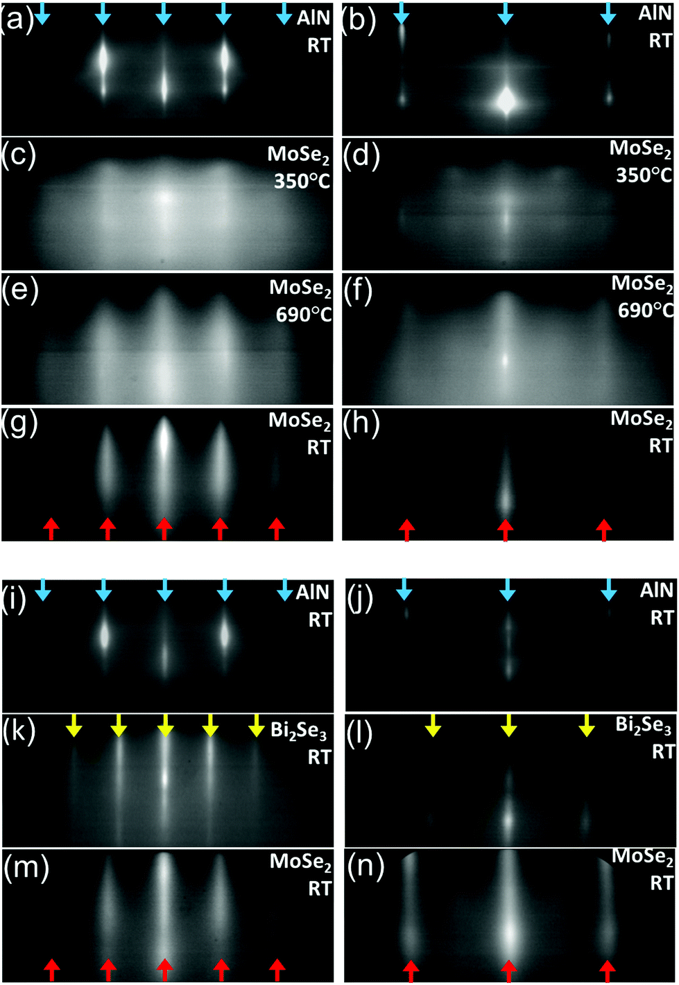 | ||
| Fig. 1 RHEED patterns of: (a–h) 1 ML MoSe2 deposited on AlN(0001) by the 2 step-process, and (i–n) 2 ML MoSe2 deposited on a 5 QL Bi2Se3 buffer layer, epitaxially grown on AlN(0001). (a) and (i) show the bare AlN(0001) pattern along the [11–20] azimuth and (b and j) bare AlN(0001) along the [1–100] azimuth. (c) and (d) are recordings at 350 °C after the deposition of MoSe2, (e) and (f) are recordings at 690 °C after the post-deposition annealing step, while (g) and (h) present the MoSe2 film on AlN after final cooling down to RT. In (e) and (f) MoSe2 becomes highly crystalline with the respective crystal orientations aligned to those of AlN, which is clearly observed after cooling down in (g) and (h). (k) and (l) show a 5 QL Bi2Se3 buffer layer grown epitaxially on AlN(0001) at 300 °C with high crystalline quality, (m) and (n) show that MoSe2 deposited on the Bi2Se3 buffer layer at 300 °C grows epitaxially, with [11–20]MoSe2//[11–20]Bi2Se3 and [1–100]MoSe2//[1–100]Bi2Se3. The blue and yellow downward arrows show AlN and Bi2Se3 streaks, respectively. The red upward arrows show MoSe2 streaks. | ||
Recently, our group reported20 the high-quality epitaxial growth of Bi2Se3 thin films on AlN(0001) substrates, which motivated us to use 5 quintuple layers (QL) of Bi2Se3 as a buffer layer for 2 ML MoSe2 overgrowth. The results in Fig. 1i–n show that both Bi2Se3 and MoSe2 layers are epitaxial and perfectly oriented with the AlN substrate, such that [11–20]MoSe2//[11–20]Bi2Se3//[11–20]AlN and [1–100]MoSe2//[1–100]Bi2Se3//[1–100]AlN. It is remarkable that MoSe2 is grown highly oriented on Bi2Se3 despite the large mismatch of about 20% between the two materials. The growth of MoSe2 is constrained to low temperatures due to the limited thermal stability of the underlying Bi2Se3 buffer, which decomposes in vacuum at temperatures higher than 300 °C. Nevertheless, the presence of the Bi2Se3 buffer layer promotes the growth of MoSe2 at much lower substrate temperatures (300 °C) compared to its direct deposition on the AlN(0001) substrate (690 °C), without reduction in epitaxial quality. The ability to reduce the growth temperature of such 2D materials could be advantageous for large-scale device manufacturing, especially for applications where heterogeneous integration with Si devices is required.
Film structural characterization
The surface structure of a 3 ML MoSe2 sample was imaged in situ by UHV–STM, as depicted in Fig. 2. The high resolution image (Fig. 2a) shows the hexagonal symmetry of the lattice. The brighter spots in Fig. 2a represent Se atoms located in the three corners of the top hexagon (Fig. 2b)24 separated by a distance of 3.3 Å, as shown in the line 1 scan in Fig. 2c. This is in good agreement with the theoretical value of the lattice constant aMoSe2 = 3.299 Å. The Mo atoms are located in the three corners of the hexagon located 1.67 Å below the top one (see also ESI, Fig. S1a†). This picture is further supported by the line 2 scan in Fig. 2d, showing that the Mo atoms are in a lower position and have a distance of ∼2 Å from neighboring Se atoms, close to the theoretical value of 1.9 Å. STM performed on a larger scale (see ESI, Fig. S2a, b†), reveals that at the low deposition temperature the sample has a root mean square (RMS) surface roughness value of 1.25 nm, which, however, significantly improves after post-deposition annealing (see ESI, Fig. S2c, d†) yielding a RMS roughness of 0.62 nm, over a scanned area of 5 × 5 μm2. The annealed sample shows a continuous film with smooth surface morphology.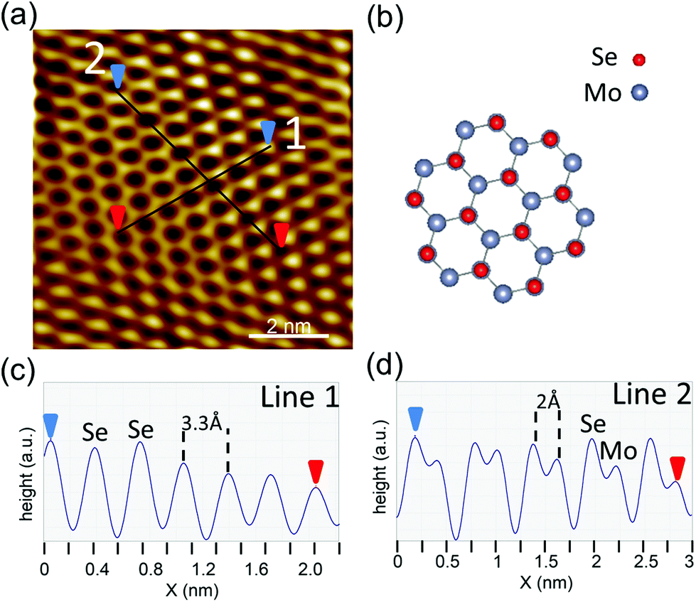 | ||
| Fig. 2 (a) Room temperature high resolution STM image of 3 ML MoSe2 on AlN(0001) (Ubias = 0.7 V, I = 0.9 nA), showing a honeycomb structure. The bright corners in the honeycomb configuration are attributed to Se atoms occupying the three corners of the topmost hexagon. (b) Stick and ball model of MoSe2 honeycomb structure along the [0001]MoSe2 axis showing the Se and Mo atom positions. The Se atoms reside on the three corners of the top hexagon while Mo occupies the three corners of a hexagon located 1.67 Å below the top one. (c) Profile along line 1 in image (a) showing the estimated distance of 3.3 Å between Se atoms, in good agreement with the MoSe2 lattice constant aMoSe2 = 3.299 Å. (d) Profile along line 2 in image (a) showing the buckling between Se and Mo atoms and their estimated lateral distance of 2 Å, close to the theoretical value of 1.9 Å. | ||
Additionally, large-area optical images of samples with different sizes and parts of the sample inspected by SEM, (see ESI, Fig. S3†) indicate a uniform, homogeneous film over the entire substrate.
The film microstructure was examined by high resolution transmission electron microscopy (HRTEM) (Fig. 3). A low-magnification cross section TEM image is presented in Fig. 3a, showing a 3 ML MoSe2 film of uniform thickness and smooth surface and interface with the AlN substrate, as also verified by large area STM images (see also ESI, Fig. S2†).
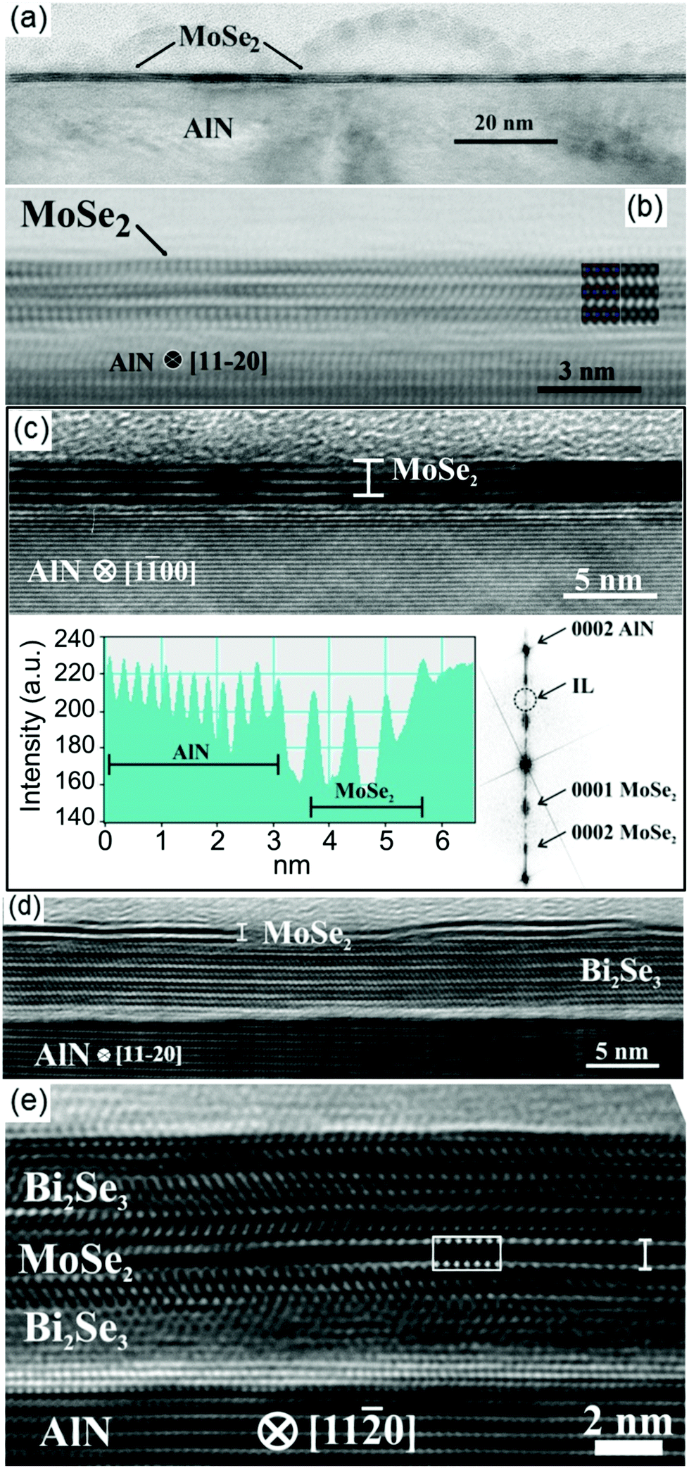 | ||
| Fig. 3 (a–c) Cross section HRTEM images of 3 ML MoSe2 grown on AlN(0001), viewed in low magnification (a) along [11–20]AlN, with the corresponding simulated image as an inset in (b), and along [1–100]AlN in (c). In (b) and (c), MoSe2 is located in the darker contrast areas, while the very bright rows, more pronounced in (c), show the separation between the MoSe2 layers. In (c) a crystalline MoSe2/AlN interface is shown with the corresponding absorption contrast profile (left side) showing lattice fringes. The fringe spacing of the top three AlN layers increases gradually. The Fast Fourier Transform (FFT) (right side), calculated from the HRTEM image, is presented showing the points that represent the spatial frequencies contained. (d) HRTEM images of 2 ML MoSe2 deposited on a 5 QL Bi2Se3 buffer layer grown on AlN(0001), viewed along [11–20]AlN. (e) 3 QL Bi2Se3/2 ML MoSe2/3QL Bi2Se3 heterostructure deposited on AlN(0001) at 300 °C, viewed along [11–20]AlN (inset, the corresponding MoSe2 simulated image). (b–e) show that MoSe2 grows epitaxially with high crystalline quality on both AlN and the Bi2Se3 buffer layer on AlN. The MoSe2 films grown on AlN show a smooth surface and interface morphology. | ||
The HRTEM image of Fig. 3b shows 3 layers of MoSe2 imaged along the [11–20]AlN zone axis. The corresponding simulated image (thickness 15 nm along the electron beam, defocus −70 nm) superimposed on the right side confirms that the [11–20] directions of the AlN and MoSe2 lattices are aligned in agreement with the RHEED data in Fig. 1. The intense bright rows correspond to the space between the MoSe2 layers (Se atoms appear dark), whilst Mo atoms are represented by the bright dotted rows in between (see also ESI, Fig. S1b†). Fig. 3c shows the same sample imaged along the [1–100]AlN zone axis. Similarly, the dark rows correspond to the MoSe2 layers and bright areas to the space between them. Because of the dense atom configuration along this direction (see also ESI, Fig. S1c†), no atoms are resolved in the dark areas in contrast to Fig. 3b. Fig. 3d and 3e show 2 ML of MoSe2 grown on top of 5 QL epitaxial Bi2Se3 buffer, and 2 ML of MoSe2 sandwiched between two Bi2Se3 layers, each 3 QL thick, respectively. The corresponding image simulation is shown as an inset in Fig. 3e (thickness 8.5 nm, defocus −70 nm), in which the bright dotted rows correspond to Mo atoms. In summary, the data in Fig. 3 (combined with the RHEED data) show that high-quality epitaxial MoSe2 and MoSe2/Bi2Se3 multilayers can be grown on AlN substrates with flat surface morphology and clean, crystalline interfaces.
A small distortion of AlN just underneath MoSe2 can be seen in Fig. 3b and 3c. The appearance of an interlayer in the TEM pictures could be attributed to an artifact. Ion milling certainly affects this interface preferentially, given the weakness of the van der Waals bonding and the fact that AlN is easily amorphized under the ion beam. In this regard, some interfacial damage is expected during sample preparation. The brighter contrast of the AlN lattice fringes at the interface could be attributed to the locally smaller thickness of the foil due to the preferential thinning mentioned above. Therefore, the interfacial region is not amorphous in the as-grown sample and any amorphization is induced by the ion milling during TEM specimen preparation.
On closer examination of the interface, we have undertaken detailed measurements of the lattice fringe spacings from the cross-sectional HRTEM images25 in Fig. 3c. Our measurements, supported by the absorption contrast profile, showed a gradual increase in the (0002) d spacing between the top 3 or 4 AlN lattice fringes, as shown in Fig. 3c. Furthermore, a strain mapping performed using geometrical phase analysis (GPA)26 (see also ESI, Fig. S4†), showed an increase of up to 20% in the spacing of these fringes. The local increase of the lattice constant could be attributed either to a change in chemical composition, or to elastic strain, or to both. Elastic strain, if present, could even promote the local amorphization of these top layers under ion beam milling. A possible cause for the increase of the d spacing is the modification of the top 3–4 AlN layers through the incorporation of molybdenum atoms. Mo has a higher electron affinity than Al, and a larger atomic radius. The absorption contrast profile in Fig. 3c shows an increase of the lattice parameter by up to ∼20% prior to the MoSe2 film. Hexagonal molybdenum nitride has a 13% larger lattice constant than AlN along the growth direction,27 so we anticipate that some elastic strain is also present. The possible reaction between MoSe2 and AlN at the interface is further studied by X-ray photoelectron spectroscopy below.
Interface and band alignment characterization by XPS
In situ X-ray photoelectron spectroscopy was applied to both MoSe2/AlN and MoSe2/Bi2Se3/AlN heterostructures. The binding energies of the Mo 3d5/2 and Se 3d5/2 core levels for 1 ML MoSe2 deposited directly on AlN(0001) (Fig. 4a and b) are 228.89 eV and 54.51 eV, respectively. These values are in good agreement with others reported18 on thin-film and bulk single-crystal MoSe2. The core level peak positions and line shapes indicate that only Mo–Se bonds exist. Therefore, within the detection limit of our XPS it can be inferred that MoSe2 does not react with the AlN substrate in large quantities. A limited incorporation of Mo in the top 3 layers of AlN may not be excluded though, taking into consideration the HRTEM analysis of the image in Fig. 3c, as described in the previous section. Similarly, in the case of 1 ML MoSe2 deposited on a 3 QL Bi2Se3 buffer layer on AlN at 300 °C (Fig. 4c and d), the Mo 3d5/2 peak position at 229.12 eV indicates Mo–Se bonds and agrees well with MoSe2 formation, while the Se 3d peak is attributed to two contributions, one to Se–Mo bonds and one to Se–Bi bonds. The Bi 4f7/2 core level binding energy of 158.52 eV (not shown here) indicates that Bi is bonded only with Se and no reaction at the Bi2Se3/AlN interface occurs. In addition, using tabulated sensitivity factors the Se/Mo ratios are found to be in the range of (1.9–2.05), indicating that the layers have stoichiometry close to the ideal, that is Se/Mo = 2/1.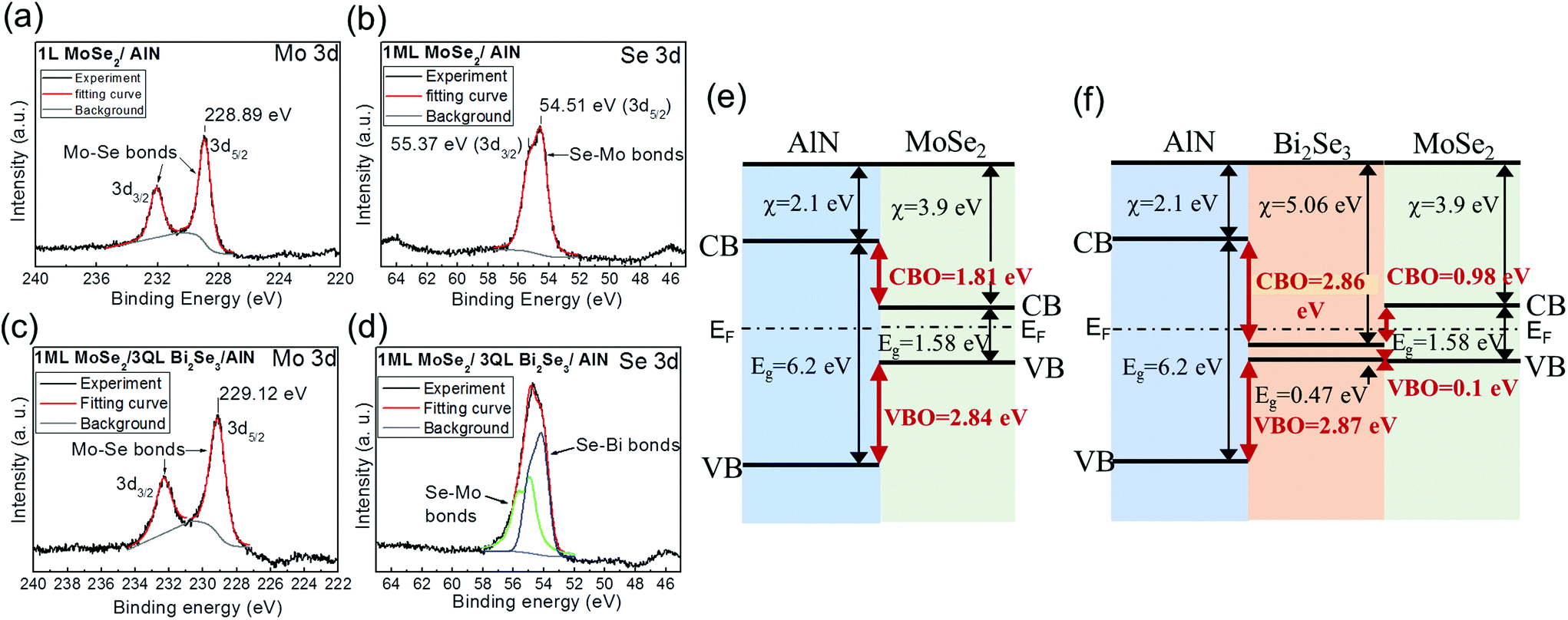 | ||
| Fig. 4 (a and b) Mo 3d and Se 3d core level XPS peaks of 1 ML MoSe2 grown on AlN. No reaction with the substrate is observed and the positions and line shapes of the Mo 3d and Se 3d peaks indicate Mo–Se bonding. (c and d) Mo 3d and Se 3d core level XPS peaks of 1 ML MoSe2 deposited on a 3QL Bi2Se3 buffer layer on AlN. The Se 3d peak is attributed to Se–Mo and Se–Bi bonding, while the Mo 3d peaks indicate Mo–Se bonding. (e and f) Schematic of the MoSe2/AlN and MoSe2/Bi2Se3/AlN band offsets, as determined by XPS core level analysis. χ and EF denote the electron affinity and the Fermi energy, respectively. Eg is the energy gap, while CBO and VBO denote the conduction and valence band offsets, respectively. | ||
The band offsets of the MoSe2/AlN and MoSe2/Bi2Se3/AlN heterojunctions were derived from XPS measurements (Fig. 4e and f). In particular, the valence band offsets (VBO) were determined using Kraut's method28 to be 2.84 eV and 2.87 eV/0.1 eV for the MoSe2/AlN and Bi2Se3/AlN systems, respectively (see also ESI†). Accordingly, the conduction band offsets (CBO) were calculated to be 1.81 eV and 2.86 eV/0.98 eV for the MoSe2/AlN and Bi2Se3/AlN systems, respectively, using band gap values (see also ESI†) taken from the literature. The estimated CBO and VBO between the MoSe2 and AlN indicate a sufficiently high transport barrier for both electrons and holes perpendicular to the layers, implying that the AlN layer could provide sufficient insulation for the operation of MoSe2-based electronic devices with minimum leakage through the substrate. It is worth noting that the XPS-reconstructed band alignments are consistent with electron affinity values, χ (see Fig. 4e and f) reported in the literature for AlN, MoSe2 and Bi2Se3 materials29–31 and the position of the Fermi level, EF, with respect to the CB and VB of the layers in the stack, suggesting that there is no band bending or charge transfer at the interfaces.
Electronic band structure of MoSe2 films
Fig. 5 shows the valence band structure of 1–6 ML MoSe2 films grown on AlN(0001) substrates, as imaged by ARPES in the ΓKHA plane of the 1st BZ of MoSe2,22,32 using He I (21.22 eV) and He II (40.814 eV) excitation energies. Except for the spin splitting of the band near K, which is not resolved because of limited resolution (∼110 meV) at room temperature, in the monolayer limit, the observed band dispersion along Γ–K (Fig. 5a and d) agrees quite well with the theoretical calculations (Fig. 5g). The valence band maximum (VBM) is located at the K point with a binding energy EB = 1 eV, about (150–200) meV higher in energy than at the Γ point. Comparison with first principles calculations (Fig. 5g), which predict a conduction band minimum (CBM) also at the K point, indicates that our nominal single-layer MoSe2 films have a direct band gap.19,33,34 As the thickness increases to 3 ML (Fig. 5b and e) and 6 ML (Fig. 5c and f), the VBM switches to the Γ/A point, due to a shift of the topmost valence band to a lower binding energy (closer to EF) around the Γ/A point, while its position at the K/H point remains at the same level. Thus, in thicker films the VBM is located at the Γ/A point (Fig. 5e and f), resulting in an indirect band gap, as predicted33 in bulk TMDs or observed19 in 8 ML-thick MoSe2 films. The thickness dependence of the VBM around the Γ/A point is clearer in the He II data (Fig. 5 d–f).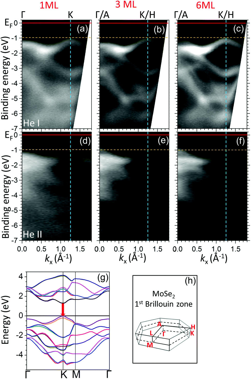 | ||
Fig. 5 Valence band structure imaging by ARPES of (1–6 ML) MoSe2 layers grown on AlN(0001) substrates along the Γ/A–K/H direction of the 1st BZ of MoSe2. Measurements made at RT, using (a–c) He I (21.22 eV) and (d–f) He II (40.814 eV) resonance radiation. The images in (a–f) show the binding energy as a function of the wavevector component k||,x parallel to the surface. In the monolayer limit (a and d) the VBM is located at the K point at EB = 1 eV, indicating a direct band gap. In thicker films, at 3 ML (b and e) and 6 ML (c and f), the VBM is located at the Γ point, consistent with an indirect band gap. Among He I and He II data for 3 ML (b and e) and 6 ML (c and f) films, small differences in the band structure around the Γ point are observed. This is attributed to a small  dispersion around the Γ point. Red solid lines indicate the EF level position, while orange dashed lines indicate the position of the VBM at the K/A point. (g) First principles-calculated band structure of 1 ML. The red arrow indicates the direct band gap position. (h) The first Brillouin zone of the 2H structure of MoSe2. dispersion around the Γ point. Red solid lines indicate the EF level position, while orange dashed lines indicate the position of the VBM at the K/A point. (g) First principles-calculated band structure of 1 ML. The red arrow indicates the direct band gap position. (h) The first Brillouin zone of the 2H structure of MoSe2. | ||
The small difference between the He I and He II data is due to a weak dispersion  around the zone center,22,32 which is picked up by the different photon excitation energies. As thickness increases, mainly Mo 4dz2 orbitals22,23,32–34 contribute to the VBM around the Γ point through the van der Waals–interlayer interaction,33 showing its bulk character. On the other hand the topmost VB around the K point shows negligible thickness dependence due to the Mo 4dxy/x2−y2 origin.22,23,32–34 The data in Fig. 5 present well resolved spectra, characteristic of energy dispersion along the ΓK crystallographic direction in k-space, in agreement with theory. This supports our claim made on the basis of RHEED in Fig. 1 that the films are highly-oriented, essentially forming a single crystal. If several orientation domains existed, then a more complex and fuzzy dispersion would have been observed in Fig. 5, characteristic of a mixture of dispersions along different crystallographic orientations, which is not the case here.
Film quality and thickness uniformity by Raman and PL
The vibrational modes of the prepared monolayer MoSe2 film on 200 nm AlN(0001)/Si(111) were investigated by Raman spectroscopy. The group theory analysis for bulk TMDs that are members of D6h point group symmetry35 predicts four Raman-active and two Raman-inactive modes. From the active modes, only the in-plane mode E12g and the out-of-plane mode A1g are accessible under the experimental conditions. Additionally, one Raman mode that is inactive in bulk crystals becomes optically active when the number of layers decreases, due to the breakdown of translational symmetry.15,35 This is an interlayer vibrational mode B12g, characterized as a breathing mode, and is present only in few-layer material and absent in a single-layer MoSe2.The typical Raman spectrum of single-layer MoSe2 on AlN shown in Fig. 6a has two intense sharp Raman peaks. One is attributed to the MoSe2 out-of-plane vibrational mode A1g at 240.8 cm−1, and one to the crystalline Si35 substrate at 521 cm−1. The in-plane E12g mode of MoSe2 is located at 288.5 cm−1 (clearly shown in the expanded Raman spectrum in the region of 200–400 cm−1 in Fig. 6d). There is no evidence of the breathing mode B2g peak around 352 cm−1, an area of the spectrum that is dominated by weak background signals. The bands centered at 303 cm−1 and 960 cm−1 (Fig. 6a) are associated with the 2TA and 2TO modes of crystalline Si.36
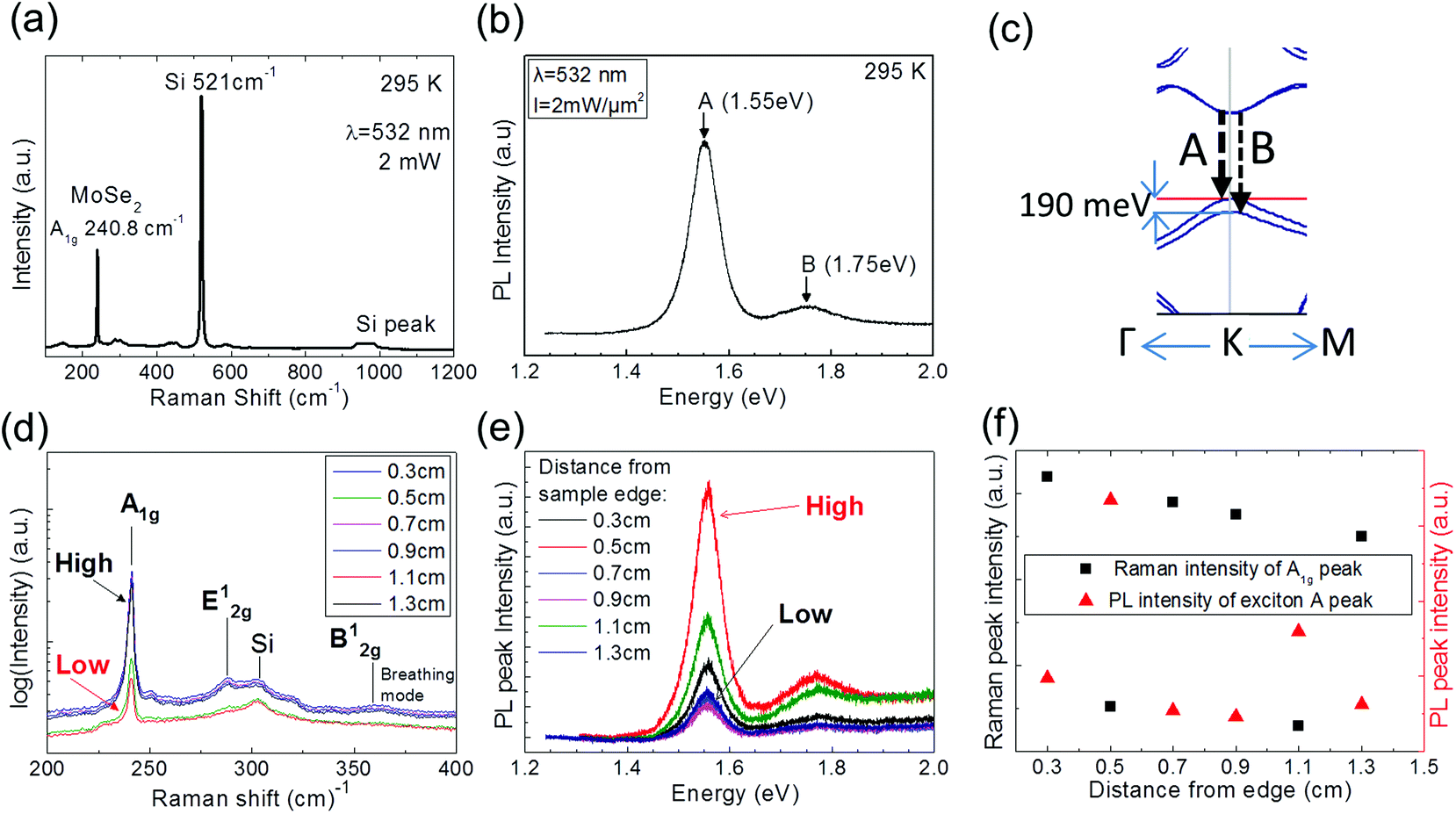 | ||
| Fig. 6 (a–c) Characterization of nominally single-layer MoSe2 on AlN(0001): (a) Raman spectrum showing the A1g peak at 240.8 cm−1 associated with MoSe2; (b) photoluminescence spectrum showing the presence of two excitonic peaks at 1.55 eV and 1.75 eV; (c) schematic detail of the theoretical band structure around the K point of 1 ML MoSe2, indicating the two excitonic transitions A and B with a 190 meV energy difference due to spin–orbit splitting. The theoretically predicted energy difference is in good agreement with the measured PL peaks energy difference in (b). (d–f) Large scale uniformity investigation of a 2 × 2 cm2 sample of the same MoSe2 sample on AlN(0001): (d) Raman spectra and (e) photoluminescence spectra measured at variable distances from the sample edge; (f) correlation of Raman and PL peak intensities measured at variable distances from the sample edge. On a large scale two different behaviors are observed: the high Raman signal of the A1g peak is correlated to the low PL intensity of exciton A and vice versa. | ||
From the peak positions of the Raman shifts and their intensities it is difficult to distinguish between monolayer and bilayer MoSe2. However, most of the evidence in this work is in favor of monolayer MoSe2, and this is in good agreement with published data of monolayer MoSe2 either transferred35,37 or grown15,17,38 on SiO2/Si substrates. The intensity ratio between the out-of-plane A1g and in-plane E12g modes (A1g/E12g) is found to be ∼23, in agreement with published values for exfoliated single-layer MoSe2.37,39 In addition, the weak or totally absent breathing mode (Fig. 6d) points to a single-layer MoSe2 material.
Photoluminescence spectroscopy was used to investigate the optical emission properties of monolayer MoSe2 grown on AlN, with the main aim to probe the quality of the layer and verify that the material has a direct band gap, as indicated by in situ ARPES. The epitaxally-grown single-layer MoSe2 on AlN presents strong PL emission at room temperature, as shown in Fig. 6b, with a dominant peak at 1.55 eV and a weaker peak at 1.75 eV, attributed to direct excitonic transitions A and B, respectively, corresponding to the transitions schematically shown in Fig. 6c. Due to loss of inversion symmetry in monolayer MoSe2, the VB degeneracy is lifted19,40 under the influence of a strong spin–orbit interaction, resulting in the VB splitting near the K point, as predicted by DFT (Fig. 6c) and probed by PL (Fig. 6b). The measured energy difference of ∼200 meV between the two PL signals agrees very well with the calculated spin–orbit splitting of ∼190 meV in Fig. 6c, as well as with published experimental15 and theoretical values.40 The strong PL signal in Fig. 6b indicates a direct gap material, in accordance with the nominally 1 ML thickness of the grown MoSe2, although the possibility of obtaining similar double-peak PL at the same energy from a bilayer MoSe2 cannot be excluded.
To extract information about uniformity in terms of structural and optical properties, the sample was probed over the entire 2 cm square substrate. On a short scale, in an area of 40 × 40 μm2, a highly uniform layer in terms of Raman A1g peak intensity, width and position was revealed (see also ESI, Fig. S5†). In general, Raman selection rules do not exclude a dependence of the Raman peak intensities on the crystal orientation, which should be reflected in the polarization of the scattered light. However, the Raman experimental set-up used here does not have an analyzer, so the detection system lacks sensitivity with respect to the polarization of the scattered radiation from the sample. Therefore, the peak intensities do not depend on the crystal orientation, as verified by arbitrarily rotating the sample (not shown here). Given the insensitivity of the different Raman peaks to crystal orientation, the intensity ratio between A1g and E12g is an appropriate parameter for an accurate uniformity assessment of the MoSe2 film. Since the E12g peak is small and overlaps with a nearby Si peak, both peaks are fitted simultaneously and the height of the E12g peak is extracted. An example of a E12g fitting result is given in Fig. S5.† It is clear that the A1g/E12g Raman mapping (see also ESI, Fig. S5†) indicates a uniform MoSe2 layer over a 40 × 40 μm2 area, with an average A1g/E12g ratio value of ∼23, indicative of monolayer MoSe2.37
On a larger scale, the sample was probed along a line that runs across the substrate from one edge to the other with 200 μm steps, and the results are summarized in Fig. 6d and e. Although the sample is very uniform over large areas, the data show a remarkable “digital” behavior mainly revealed in the Raman spectra (Fig. 6d). The Raman A1g mode acquires either low or high values but no values in between. The PL (Fig. 6e) follows a similar behavior although with a larger dispersion in intensity. However, correlation with the Raman peak is observed: the PL intensity is high where the Raman intensity of A1g is low and vice versa (Fig. 6f), a behavior that is not fully understood. Based on previous PL work on MoS2,4,41 it is tempting to associate the low Raman/high PL behavior with the presence of single-layer MoSe2 areas and the high Raman/low PL behavior with bilayer MoSe2 in other areas on the same wafer. This has to be treated with caution though, given that an abnormally high PL at room temperature has been reported37 in few-layer MoSe2. Finally, it is worth noting that uncapped single and bilayer MoSe2 have been examined by Raman and PL over a period of time and they have been found to be very stable over at least two weeks while exposed to air (see also ESI, Fig. S6†).
Critical assessment of microstructure and uniformity
The characterization of large-area MoSe2 films is very challenging because most of the techniques that are sensitive to microstructure such as HRTEM are sampling techniques probing only a limited area of the order of 80–100 nm in length. On such a length scale, the single crystal quality and thickness uniformity is unambiguously confirmed (Fig. 3) in several sampled areas on the wafer. Low magnification TEM can provide information about thickness uniformity on the few hundred nm scale, as for example the TEM image in Fig. S7 (ESI†), which shows a very good thickness uniformity of MoSe2 over a region that exceeds 250 nm in length. Other techniques such as STM or SEM probe larger areas on the few tens of a micron or mm scales, and by using these techniques (see also ESI, Fig. S2 and S3†) we conclude that the films are continuous with full coverage over the entire 2 inch diagonal substrate, and that there are no major thickness variations across the wafer. However, these techniques are less sensitive to thickness variations at the level of a single atomic layer and to the existence of microstructures such as grains.Orientational grain boundaries (GB) retain a crystalline structure and may be of high or low angle. In this case, the pertinent high angle GBs are the orientation twins that have not been identified in our films by RHEED, as already discussed above in connection to Fig. 1. The cross-sectional HRTEM observations are also consistent, i.e. no twin boundaries were observed.
Regarding low-angle GBs, plan view TEM observations are required. The preparation of such TEM specimens is difficult due to the AlN substrate, which renders useless the currently available approaches. Although it was not possible to account for such GBs from plan view TEM, we argue that if they are present to any significant extent, such GBs would consist of dislocations parallel to the growth direction. In our cross-sectional observations we did not observe any appreciable density of such defects.
The characterization and uniformity assessment of ultrathin (a few ML) MoSe2 films remain big challenges. In fact, most of the techniques, including XRD, are not sensitive when applied to atomic-scale materials. Raman is a technique that has sufficient sensitivity for single-layer crystals and is extensively used for graphene and 2D MX2-type semiconductors. This provides a rough estimate about thickness and physical properties with micron resolution probing uniformity over a 10–100 μm scale at least. The MoSe2 films mapped by Raman over such a range were found to have excellent uniformity, while the same tests repeated in several parts of the wafer yielded similar excellent uniformity results.
In summary, despite the difficulties in the characterization of ultrathin films on a large area of the substrate, our investigation using a variety of techniques provides evidence that the films are continuous, covering the entire substrate, and that they do not have gross non-uniformities with respect to the thickness and the surface roughness. Moreover, electron diffraction (RHEED) and HRTEM show no evidence for randomly-oriented grains or for high- (twin) or low-angle orientational grains suggesting highly-oriented single-crystal films, epitaxially grown on cm-scale AlN substrates.
Conclusions
Here, we demonstrate the molecular beam epitaxial growth of large-area, highly-oriented single crystals of controllable single- to few-layer MoSe2 films on AlN(0001)/Si substrates. We show by HRTEM that MoSe2 films on AlN(0001) have high structural quality and surface and interface morphology, confirmed also by XPS data showing stoichiometric MoSe2 with no reaction at the interface with AlN. In addition, very good uniformity and excellent stability in air is evidenced by room temperature Raman and photoluminescence. We also show that MoSe2 can grow with very good quality on Bi2Se3 buffer layers and that epitaxial Bi2Se3/MoSe2 multilayers can be produced. As a final remark, the important role of the substrate is emphasized here. Since AlN is a wide band gap material, it offers the benefits of the MoSe2 semiconductor-on-insulator integration scheme, creating the prospect for low leakage through the substrate and improved electrostatic control. This is further supported by XPS analysis, which indicates sufficiently high CBO and VBO acting as barriers for charge transport through the substrate. Moreover, AlN/Si(111) large-area (200 mm and 300 mm) wafers are readily available as they have been developed for several years in the context of III-nitride power and lighting devices. Once high quality epitaxial MoSe2 is prepared on 300 mm AlN/Si wafers, devices and circuits can be realized on the same wafers, or the MoSe2 layer can be transferred onto other optimal large-area substrates of choice, including flexible or transparent substrates for further device processing. Therefore AlN/Si creates the prospect for low-cost wafer-scale manufacturing of MoSe2-based devices and circuits when TMD technology becomes mature enough for volume production.Acknowledgements
The work is supported by the ERC Advanced Grant SMARTGATE-291260 and the National program of excellence (ARISTEIA-745) through the project TOP-ELECTRONICS.Notes and references
- Q. H. Wang, K. Kalantar-Zadeh, A. Kis, J. N. Coleman and M. S. Strano, Nat. Nanotechnol., 2012, 7, 699–711 CrossRef CAS PubMed.
- M. Xu, T. Lian, M. Shi and H. Chen, Chem. Rev., 2013, 113, 3766–3798 CrossRef CAS PubMed.
- A. K. Geim and I. V. Grigorieva, Nature, 2013, 499, 419–425 CrossRef CAS PubMed.
- K. F. Mak, C. Lee, J. Hone, J. Shan and T. F. Heinz, Phys. Rev. Lett., 2010, 105, 136805 CrossRef.
- H. S. Lee, S. W. Min, Y. G. Chang, M. K. Park, T. Nam, H. Kim, J. H. Kim, S. Ryu and S. Im, Nano Lett., 2012, 12, 446–701 CrossRef PubMed.
- H. Fang, C. Battaglia, C. Carraro, S. Nemsak, B. Ozdol, J. S. Kang, H. A. Bechtel, S. B. Desai, F. Kronast, A. A. Unal, G. Conti, C. Conlon, G. K. Palsson, M. C. Martin, A. M. Minor, C. S. Fadley, E. Yablonovich, R. Maboudian and A. Javey, Proc. Natl. Acad. Sci. U. S. A., 2014, 111, 6198–6202 CrossRef CAS PubMed.
- J. S. Ross, P. Klement, A. M. Jones, N. J. Ghimire, Y. Yan, D. G. Mandrus, T. Taniguchi, K. Watanabe, K. Kitamura, W. Yao, D. H. Cobden and X. Xu, Nat. Nanotechnol., 2014, 9, 268–272 CrossRef CAS PubMed.
- A. Pospischil, M. M. Furchi and T. Mueller, Nat. Nanotechnol., 2014, 9, 257–261 CrossRef CAS PubMed.
- B. Radisavljevic, A. Radenovic, J. Brivio, V. Giacometti and A. Kis, Nat. Nanotechnol., 2011, 6, 147–150 CrossRef CAS PubMed.
- H. Liu, A. T. Neal and P. D. Ye, ACS Nano, 2012, 6, 8563–8569 CrossRef CAS PubMed.
- H. Liu and P. D. Ye, IEEE Electron Device Lett., 2012, 33(4), 546–548 CrossRef CAS.
- B. Radisavljevic, M. B. Whitwick and A. Kis, ACS Nano, 2011, 5, 9934–9938 CrossRef CAS PubMed.
- H. Wang, L. Yu, Y. H. Lee, Y. Shi, A. Hsu, M. L. Chin, L. J. Li, M. Dubey, J. Kong and T. Palacios, Nano Lett., 2012, 12, 4674–4680 CrossRef CAS PubMed.
- Y-H Lee, X. Q. Zhang, W. Zhang, M. T. Chang, C. T. Lin, K. D. Chang, Y. C. Yu, J. T. W. Wang, C. S. Chang, L. J. Li and T. W. Lin, Adv. Mater., 2012, 24, 2320–2325 CrossRef CAS PubMed.
- X. Lu, J. Lin, M. I. B. Utama, X. Gong, J. Zhang, Y. Zhao, S. T. Pantelides, J. Wang, Z. Dong, Z. Liu, W. Zhou and Q. Xiong, Nano Lett., 2014, 14, 2419–2425 CrossRef CAS PubMed.
- X. Wang, Y. Gong, G. Shi, W. L. Chow, K. Keyshar, G. Ye, R. Vajtai, J. Lou, Z. Liu, E. Ringe, B. K. Tay and P. M. Ajayan, ACS Nano, 2014, 8, 5125–5131 CrossRef CAS PubMed.
- J. C. Shaw, H. Zhou, Y. Chen, N. O. Weiss, Y. Liu, Y. Huang and X. Duan, Nano Res., 2014, 7, 1–7 CrossRef.
- F. S. Ohuchi, B. A. Parkinson, K. Ueno and A. Koma, J. Appl. Phys., 1990, 68, 2168–2175 CrossRef CAS PubMed.
- Y. Zhang, T. R. Chang, B. Zhou, Y. T. Cui, H. Yan, Z. Liu, F. Schmitt, J. Lee, R. Moore, Y. Chen, H. Lin, H. T. Jeng, S. K. Mo, Z. Hussain, A. Bansil and Z. X. Shen, Nat. Nanotechnol., 2014, 9, 111–115 CrossRef CAS PubMed.
- P. Tsipas, E. Xenogiannopoulou, S. Kassavetis, D. Tsoutsou, E. Golias, C. Bazioti, G. P. Dimitrakopulos, P. Komninou, H. Liang, M. Caymax and A. Dimoulas, ACS Nano, 2014, 8, 6614–6619 CrossRef CAS PubMed.
- P. A. Stadelmann, Ultramicroscopy, 1987, 21, 131–145 CrossRef CAS.
- R. Coehoorn, C. Haas, J. Dijkstra, C. J. F. Flipse, R. A. de Groot and A. Wold, Phys. Rev. B, 1987, 35, 6195–6202 CrossRef CAS.
- S. K. Mahatha, K. D. Patel and K. S. R. Menon, J. Phys.: Condens. Matter, 2012, 24, 475504 CrossRef CAS PubMed.
- K. Momma and F. Izumi, J. Appl. Crystallogr., 2011, 44, 1272–1276 CrossRef CAS.
- D. Gerthsen, E. Hahn, B. Neubauer, V. Potin, A. Rosenauer and M. Schowalter, Phys. Status Solidi C, 2003,(6), 1668–1683 CrossRef CAS.
- M. J. Hÿtch, F. Houdellier, F. Hüe and E. Snoeck, Nature, 2008, 453, 1086–1089 CrossRef PubMed.
- A. Bezinge, K. Yvon, J. Muller, W. Lengaeur and P. Ettmayer, Solid State Commun., 1987, 63, 141 CrossRef CAS.
- E. Kraut, R. Grant, J. Waldrop and S. Kowalczyk, Phys. Rev. Lett., 1980, 44, 1620 CrossRef CAS.
- C. I. Wu, A. Kahn, E. S. Hellman and D. N. E. Buchanan, Appl. Phys. Lett., 1998, 73, 1346–1348 CrossRef CAS PubMed.
- C. Gong, H. Zhang, W. Wang, L. Colombo, R. M. Wallace and K. Cho, Appl. Phys. Lett., 2013, 103, 053513 CrossRef PubMed.
- J. Suh, D. Fu, X. Liu, J. K. Furdyna, K. M. Yu, W. Walukiewicz and J. Wu, Phys. Rev. B: Condens. Matter Mater. Phys., 2014, 89, 115307 CrossRef.
- T. Böker, R. Severin, A. Müller, C. Janowitz, R. Manzke, D. Voss, P. Krüger, A. Mazur and J. Pollman, Phys. Rev. B: Condens. Matter, 2001, 64, 235305 CrossRef.
- W. S. Yun, S. W. Han, S. C. Hong, I. G. Kim and J. D. Lee, Phys. Rev. B: Condens. Matter Mater. Phys., 2012, 85, 033305 CrossRef.
- S. Horzum, H. Sahin, S. Cahangirov, P. Cudazzo, A. Rubio, T. Serin and F. M. Peeters, Phys. Rev. B: Condens. Matter Mater. Phys., 2013, 87, 125415 CrossRef.
- P. Tonndorf, R. Schmidt, P. Böttger, X. Zhang, J. Börner, A. Liebig, M. Albrecht, C. Kloc, O. Gordan, D. R. T. Zahn, S. Michaelis de Vasconcellos and R. Bratschitsch, Opt. Express, 2013, 21, 4908 CrossRef CAS PubMed.
- T. A. Harriman, D. A. Lucca, J. K. Lee, M. J. Klopfstein, K. Herrmann and M. Nastasi, Nucl. Instrum. Methods Phys. Res., Sect. B, 2009, 267, 1232–1234 CrossRef CAS PubMed.
- S. Tongay, J. Zhou, C. Ataca, K. Lo, T. S. Matthews, J. Li, J. C. Grossman and J. Wu, Nano Lett., 2012, 12, 5576–5580 CrossRef CAS PubMed.
- J. Mann, Q. Ma, P. M. Odenthal, M. Isarraraz, D. Le, E. Preciado, D. Barroso, K. Yamaguchi, G. von Son Palacio, A. Nguyen, T. Tran, M. Wurch, A. Nguyen, V. Klee, S. Bobek, D. Sun, T. F. Heinz, T. S. Rahman, R. Kawakami and L. Bartels, Adv. Mater., 2014, 26, 1399–1404 CrossRef CAS PubMed.
- N. Kumar, Q. Cui, F. Ceballos, D. He, Y. Wang and H. Zhao, Nanoscale, 2014, 6, 4915–4919 RSC.
- Z. Y. Zhu, Y. C. Cheng and U. Schwingenschlögl, Phys. Rev. B: Condens. Matter Mater. Phys., 2011, 84, 153402 CrossRef.
- A. Splendiani, L. Sun, Y. Zhang, T. Li, J. Kim, C. Y. Chim, G. Galli and F. Wang, Nano Lett., 2010, 10, 1271–1275 CrossRef CAS PubMed.
Footnote |
| † Electronic supplementary information (ESI) available: crystal structure of MoSe2; large area STM images of 3 ML MoSe2/AlN; large area optical and SEM images of MoSe2 films on AlN; GPA lattice strain analysis map of 3 ML MoSe2 deposited on AlN; band diagram reconstruction of MoSe2/AlN and MoSe2/Bi2Se3/AlN; short-scale uniformity investigation of 1 ML MoSe2 on AlN(0001); stability investigation of 1 ML MoSe2 on AlN(0001); large area TEM image of MoSe2 on AlN(0001). See DOI: 10.1039/c4nr06874b |
| This journal is © The Royal Society of Chemistry 2015 |