
 Open Access Article
 This Open Access Article is licensed under a
 Creative Commons Attribution 3.0 Unported Licence
Doping of single-walled carbon nanotubes controlled via chemical transformation of encapsulated nickelocene
Marianna V.
Kharlamova
*a,
Markus
Sauer
a,
Takeshi
Saito
b,
Yuta
Sato
b,
Kazu
Suenaga
b,
Thomas
Pichler
a and
Hidetsugu
Shiozawa
*a
aFaculty of Physics, University of Vienna, Strudlhofgasse 4, 1090 Vienna, Austria. E-mail: mv.kharlamova@gmail.com; hidetsugu.shiozawa@univie.ac.at; Fax: +43 14277 51475; Tel: +43 14277 51466
bNanotube Research Center, AIST, 1-1-1 Higashi, Tsukuba 305-8565, Japan
First published on 28th November 2014
Abstract
Controlled doping of carbon nanotubes is elemental for their electronic applications. Here we report an approach to tune the polarity and degree of doping of single-walled carbon nanotubes via filling with nickelocene followed by encapsulated reactions. Using Raman, photoemission spectroscopy and transmission electron microscopy, we show that nickelocene molecules transform into nickel carbides, nickel and inner carbon nanotubes with reaction temperatures as low as 250 °C. The doping efficiency is determined for each chemical component. Synchronous charge transfer among the molecular components allows bipolar doping of the carbon nanotubes to be achieved in a broad range of ±0.0012 e− per carbon.
1. Introduction
Single-walled carbon nanotubes (SWCNTs) possess unique physical, chemical and mechanical properties that are defined by their atomic structure.1 Since their discovery2,3 attempts were made to tailor the electronic properties towards applications in nanoelectronics such as logic elements, memory devices and electron field emitters.4,5 Over the last few years several methods have been established. These methods include chemisorption and physisorption of atoms and molecules on the nanotube outer surface, substitution of carbon with other elements, intercalation of carbon nanotube bundles and filling tubular interior channels.6 Among these methods, filling of carbon nanotubes is a very effective way to modify the electronic structure and the chemical environment in a controlled way. This is due to the fact that the SWCNT interiors can be filled with substances having different chemical and physical properties.7–11 It allows the SWCNT electronic properties to be modified via the encapsulation of donor or acceptor molecules.12–21 Because the encapsulated chemicals are much less affected by environmental factors,22 endohedral filling is a promising route towards the functionalisation of carbon nanotubes for electronic applications.Organometallic and coordination compounds are promising functional fillers as reported in some of the early studies with metallocenes,23–25 metal phthalocyanine,26 and metal acetylacetonates.27 Only a few papers were dedicated to theoretical and experimental studies of the electronic properties of metallocene-filled SWCNTs. On the theoretical side, it has been shown that encapsulation of different metallocenes (C5H5)2M, where M is a metal center, leads to electron doping of SWCNTs that depends on their chirality and the type of metal atom.28–31 On the experimental side, electron doping was observed for SWCNT encapsulating ferrocene25,32–35 and cerocene,36,37 where low doping levels were achieved.
Encapsulated inside SWCNTs, organometallic molecules can be reacted to form metallic particles that subsequently catalyse the formation of inner carbon nanotubes in a confined tubular environment.25,27 It was shown that such endohedral reactions can lead to changes in the electron doping of SWCNTs only to lower levels.32
The control of both electron and hole doping of SWCNTs at the highest possible levels using one precursor would make the endohedral process promising as a functionalisation route for carbon nanotubes. Furthermore, finding a molecular precursor that can be reacted at reduced temperatures is a prerequisite for the method to be adapted in a process line for device fabrication.
In the present work we synthesise nickelocene (NiCp2)-filled SWCNTs and study their physical properties in response to heating under vacuum. We demonstrate that SWCNTs can be filled with nickelocene with a large filling factor. Using Raman spectroscopy we show that at temperatures ranging from 250 °C to 1200 °C nickelocene molecules react with one another to grow inner tubes inside the outer SWCNTs at high yield. The chemical state of the encapsulated compounds has been analysed at every annealing step by X-ray photoelectron spectroscopy (XPS). The formation of metallic clusters has been observed by transmission electron microscopy (TEM). The electronic structure of SWCNTs has been studied by XPS and ultraviolet photoelectron spectroscopy (UPS). By tracing the carbon π peak energy in the valence band spectra, we show that different chemical states of the SWCNT interior allow both electron and hole doping of the SWCNTs at high doping levels, as illustrated in Fig. 1. Our results demonstrate that the chemical transformation of nickelocene can be utilized for the directional modification of the SWCNT electronic properties at reaction temperatures as low as 250 °C.
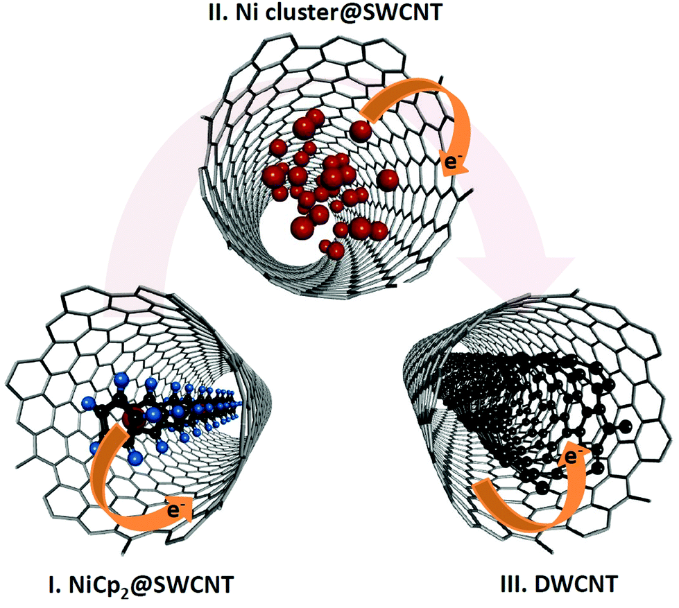 | ||
| Fig. 1 Schematic of electron bipolar doping of SWCNTs via the chemical transformation of encapsulated nickelocene. | ||
2. Experimental
Single-walled carbon nanotubes with a mean diameter of 1.7 nm38 were synthesised by the enhanced direct injection pyrolytic synthesis (e-DIPS) method. SWCNT buckypapers were pre-heated in air at 500 °C for one hour. Filling with nickelocene (NiCp2, chemical formula C10H10Ni) was done by heating the buckypapers with NiCp2 powder inside a vacuum (better than 5 × 10⁻⁶ mbar) sealed Pyrex-glass tube at 50 °C for five days. A conversion of nickelocene-filled SWCNTs to DWCNTs was carried out via annealing at temperatures in the range of 250–1200 °C for 2 hours in a vacuum chamber evacuated to a pressure better than 2 × 10⁻⁶ mbar. Raman spectroscopy measurements were performed at room temperature using a Horiba Jobin Yvon LabRAM spectrometer equipped with a HeNe laser that operates at a wavelength of 633 nm (Eex = 1.96 eV). The radial breathing mode (RBM) lines in the Raman spectra were fitted to Voigt peaks and the area intensities were calculated using PeakFit v4.12. TEM was performed with a JEOL JEM-2100F microscope equipped with Delta spherical aberration (Cs) correctors39 at an accelerating voltage of 60 kV. X-ray and ultraviolet photoemission spectra were recorded with monochromatic Al Kα (1486.6 eV) and He II (40.8 eV) radiation, respectively, using a hemispherical SCIENTA RS4000 photoelectron energy analyzer. The experimental resolution and the Fermi energy were determined from the Fermi edge of clean Au substrates. The overall energy resolutions were better than 20 meV for ultraviolet and 450 meV for X-ray photoemission spectroscopy. All photoemission measurements were carried out at room temperature.3. Results and discussion
3.1. Formation of double-walled carbon nanotubes
Raman spectroscopy is a non-destructive method well suited for observing the formation of carbon nanotubes. It has been proven to be a valuable tool to analyze the transformation of filled SWCNTs into DWCNTs. Examples are nanotubes containing molecules like fullerenes,40 ferrocene,25,41,42 cerocene36 and platinum acetylacetonate.27Fig. 2a shows the evolution of the RBM-band of SWCNTs’ Raman spectra acquired at a laser wavelength of 633 nm (Eex = 1.96 eV) upon filling with nickelocene and subsequent annealing at temperatures of 400–1200 °C. The RBM-band of the pristine SWCNTs is located at frequencies ranging from 125 to 160 cm−1. After filling with nickelocene the RBM lines are upshifted by 4 cm−1, as previously observed for SWCNTs filled with other molecules.25,27,36,43 After annealing they are shifted back to the original position and additional peaks appear at 212, 216 and 253 cm−1. Taking into consideration that the position of RBM peaks is inversely proportional to the nanotube diameter,44 these new peaks are of inner tubes whose diameters are smaller than those of the outer tubes. Note that the inner tube peak being as high as the outer tube peak means that DWCNTs are produced in a high yield as a consequence of a high filling degree of the SWCNTs with nickelocene. Notably, the largest inner tube peak is composed of two lines, one at 212 cm−1 assigned to the (12,3) nanotube with a diameter of 1.08 nm and the other at 216 cm−1 assigned to the (13,1) tube with a diameter of 1.06 nm. The peak located at 253 cm−1 is of the (11,1) tube with a diameter of 0.91 nm.40,41,45 Given a mean diameter of the pristine SWCNTs (1.7 nm) and a van der Waals distance (0.335 nm) between the outer and inner graphene layers of DWCNTs, we estimated an inner tube mean diameter of ∼1.03 nm. The (12,3) and (13,1) tubes fall in a diameter range near the mean value, which allows us to evaluate the growth of the majority of inner tubes. Fig. 2b shows the area intensity of the peak composed of (12,3) and (13,1) tubes normalized to the intensity of the outer tube peak plotted against annealing temperature. The inner tubes grow rapidly with raising the temperature from 400 to 700 °C at and above which reactions to growth of inner tubes seem to be completed within 2 hours.
 | ||
| Fig. 2 (a) Raman spectra of the pristine, nickelocene-filled SWCNTs and samples annealed at temperatures between 400 °C and 1200 °C for 2 h measured at a laser wavelength of 633 nm (Eex = 1.96 eV), vertically offset by an arbitrary constant for clarity. a.u. refers to arbitrary units. (b) Total area intensity of the (12,3) and (13,1) RBM peaks normalized to the outer tube RBM peak area plotted against annealing temperature. | ||
3.2. Chemical transformation of nickelocene
High-resolution TEM observations reveal nickel clusters formed inside SWCNTs by annealing, Fig. 3. From X-ray photoemission spectroscopy we gain further insights into the chemical transformation of nickelocene inside SWCNTs. Fig. 4a shows the Ni 2p spectra of the nickelocene-filled SWCNTs and those annealed at 250–1200 °C for 2 hours. The spectrum of the NiCp2-filled SWCNTs exhibits two sharp peaks located at 854.53 eV and 871.80 eV binding energies, corresponding to the Ni 2p3/2 and Ni 2p1/2 edges, respectively. These peaks are not observed in the spectrum of the pristine SWCNTs. The energy positions are very similar to those reported previously for nickelocene absorbed on Ag(100).46 | ||
| Fig. 3 TEM micrograph of NiCp2-filled SWCNTs after being annealed at 500 °C for 2 hours, exhibiting crystalline metals encapsulated inside SWCNTs. | ||
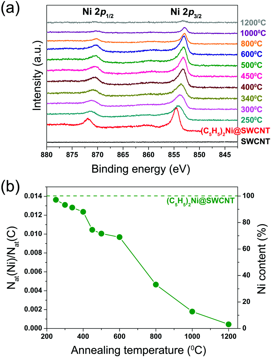 | ||
| Fig. 4 (a) Ni 2p X-ray photoelectron spectra of the pristine SWCNTs, nickelocene-filled SWCNTs and samples annealed for 2 h at 250–1200 °C, vertically offset by an arbitrary constant. (b) Nickel-to-carbon atomic ratio and nickel content at every annealing step. The dashed horizontal line is the value for the NiCp2-filled SWCNTs before annealing. | ||
The Ni 2p spectra of the annealed samples show a successive downshift of the Ni 2p3/2 and Ni 2p1/2 peaks at increasing temperature. The Ni 2p3/2 peak positions are summarized in Table 1. At the first three consecutive annealing steps at 250 °C, 300 °C and 340 °C, the Ni 2p3/2 and Ni 2p1/2 peaks are downshifted by 0.42 eV, 0.39 eV and 0.15 eV, respectively, and become much broader than the corresponding peaks of the NiCp2-filled SWCNTs. Both features can be attributed to changes in the chemical state of nickel due to the formation of different nickel and carbon alloys (NixC) following the decomposition of nickelocene. Upon annealing at temperatures above 400 °C they are further narrowed and downshifted and reach the energies for metallic nickel (Ni 2p3/2 peak is at ∼853 eV47,48) at 600 °C. The data suggest that the initially formed nickel carbides transform into more stable metallic nickel. This is in line with previous reports that nickel carbides (in particular, Ni3C) are metastable49 and that Ni3C decomposes at temperatures higher than 400–500 °C.50–52 TEM observations confirm that the nickel clusters are encapsulated inside SWCNTs, see Fig. 3. At temperatures higher than 800 °C, nickel atoms are released rather quickly from the nanotubes, seen as reduced nickel Ni 2p signals to 3% of the initial quantity at 1200 °C.
| Temperature (°C) | N at(Ni)/Nat(C) | Ni content (%) | Ni 2p3/2 (eV) | π (eV) |
|---|---|---|---|---|
| SWCNT | 3.18 | |||
| NiCp2@SWCNT | 0.0141 | 100 | 854.53 | 3.25 (+0.07) |
| 250 | 0.0136 | 97 | 854.11 (−0.42) | 3.36 (+0.18) |
| 300 | 0.0131 | 93 | 853.72 (−0.81) | 3.31 (+0.13) |
| 340 | 0.0128 | 91 | 853.57 (−0.96) | 3.29 (+0.11) |
| 400 | 0.0124 | 88 | 853.22 (−1.31) | 3.28 (+0.10) |
| 450 | 0.0105 | 74 | 853.17 (−1.36) | 3.26 (+0.08) |
| 500 | 0.0100 | 71 | 853.12 (−1.41) | 3.26 (+0.08) |
| 600 | 0.0096 | 69 | 853.05 (−1.48) | 3.20 (+0.02) |
| 800 | 0.0047 | 33 | 852.90 (−1.63) | 3.06 (−0.12) |
| 1000 | 0.0018 | 13 | 852.99 (−1.54) | 3.02 (−0.16) |
| 1200 | 0.0004 | 3 | 853.04 (−1.49) | 3.00 (−0.18) |
From the area intensity ratio between the Ni 2p and C 1s edge photoelectron peaks, taking the photoemission cross sections into account, we calculate the number of nickel atoms relative to carbon atoms. For the NiCp2-filled sample this value Nat(Ni)/Nat(C) equals 0.0141. This is about 4.5 times as large as 0.0031 reported for ferrocene-filled SWCNTs,25,32 which testifies to a high filling degree of SWCNTs with nickelocene, and is in agreement with the Raman spectroscopy data discussed in the previous section. The calculated nickel-to-carbon atomic ratios Nat(Ni)/Nat(C) as well as Ni contents defined as the atomic ratios normalized by the value of NiCp2-filled SWCNTs are plotted in Fig. 4b and summarized in Table 1.
Upon annealing at temperatures below 400 °C the Ni content is reduced only to 90% or higher. At 450–600 °C it goes down to 69%. The loss becomes substantial at higher temperatures. The quantity of nickel is reduced to 33% at 800 °C, equals 13% at 1000 °C, and then at 1200 °C almost all nickel atoms are removed from the sample (Fig. 4b). The loss of nickel atoms is in line with observations on the annealed ferrocene-filled SWCNTs.25 However, for ferrocene no metallic nanoparticles could be achieved; only stable iron carbide is formed. In the present case, nickel carbides are initially formed at temperatures in the range of 250–400 °C and then transformed entirely into metallic nickel at 600 °C. As seen in Fig. 2b, the majority of inner tubes are formed within the temperature range of 450–650 °C where nickel carbides are transformed into metallic nickel. This suggests that nickel clusters act as catalysts for the growth of inner tubes, which ends when no more carbon atoms are available.
3.3. Charge transfer and bonding environment
Ultraviolet photoelectron spectroscopy provides further insights into the electronic structure of the filled SWCNTs and its response to the interior chemical transformation. Fig. 5 shows the valence band spectra of the pristine, nickelocene-filled SWCNTs and samples heated at 250–1200 °C for 2 hours. The spectra exhibit two characteristic peaks of nanotube's sp2 orbitals located at about 3 eV and 8 eV that correspond to the π- and σ-band, respectively.53,54 Because of the broad diameter distribution of pristine nanotubes, the one-dimensional van Hove singularities are not very pronounced. In the spectrum of NiCp2-filled SWCNTs there is a broad peak located at binding energies from 0.6 to 1.9 eV. This peak is not observed for the pristine SWCNTs and vanishes after annealing, and hence can be assigned to the highest occupied molecular orbital of nickelocene. After the filling, the nanotube's π-peak is shifted by 0.06 eV to a higher binding energy. An upshift of the π-peak was observed previously in the valence band spectra of SWCNTs intercalated with alkali metals55,56 and filled with ferrocene.25,32 Hence, this energy shift is confidently attributed to the electron transfer from the encapsulated nickelocene to the SWCNTs. | ||
| Fig. 5 Valence band spectra of the pristine, nickelocene-filled SWCNTs and samples annealed at 250–1200 °C for 2 h, vertically offset by an arbitrary constant. | ||
Furthermore, doping of the outer tubes can be traced by monitoring the π-peak energy shift at every annealing step, see Fig. 6a and Table 1. At 250 °C the π peak upshifts to a higher binding energy to reach a largest positive shift of 0.18 eV relative to the pristine SWCNT's position. The energy shift becomes nearly zero at 600 °C, turns negative at higher temperatures, and reaches a maximum negative shift of −0.18 eV at 1200 °C. The π peak shifts to lower binding energies, which were reported recently for carbon nanotubes filled with copper57 and zinc halogenides,58 can be attributed to hole doping of the SWCNTs. All photoemission data support that the charge transfer can be tuned via the chemical transformation that allows both electron and hole doping of SWCNTs to be achieved at different levels.
 | ||
| Fig. 6 (a) Fermi level shifts for the NiCp2-filled SWCNTs annealed at 250–1200 °C. Right vertical axes are the corresponding number of electrons transferred to SWCNT's carbon atom Ntotal (e− per carbon) and the charge transfer density per nanotube length CT (e− Å−1). Dashed horizontal lines denote the values for the pristine and NiCp2-filled SWCNTs. (b–d) Schematics for electron or hole doping of SWCNTs in pristine and annealed NiCp2-filled SWCNTs. | ||
Doping of nanotubes is controlled by several processes that are dependent on annealing temperature: (i) chemical transformation of nickelocene, (ii) growth of inner tubes, and (iii) evaporation of nickel. Nickelocene, nickel carbides and metallic nickel have an electron doping effect on the SWCNTs. It leads to the upshift of the Fermi level with respect to the SWCNT's density of states (Fig. 6b and c). In turn, we observed that the growth of inner tubes starts at 400 °C. This means that the SWCNTs annealed at temperatures higher than 400 °C contain carbon inner tubes as well as nickel compounds. The latter evaporates at high temperatures, which leaves pure DWCNTs after annealing at 1200 °C. In DWCNTs there is electron transfer from the outer tube to the inner tube (Fig. 6d).
For a quantitative analysis, we calculate the total number of transferred electrons per outer tube carbon atom Ntotal (e− per carbon) and the charge transfer density per nanotube length CT (e− Å−1) by comparing the Fermi level shifts with those for potassium-doped SWCNTs55 (Fig. 6a and Table 2). Ntotal = 0.00046 e− per carbon is obtained for the nickelocene-filled SWCNTs. Provided that the 1.7 nm diameter SWCNT has 20.32 carbon atoms per 1 Å of length, this corresponds to CT = 0.00933 e− Å−1. At 250 °C the values jump to maxima of 0.00118 e− per carbon and 0.02399 e− Å−1, then drop steeply, become negative with increasing temperature, and hit negative maxima of −0.00118 e− per carbon and −0.02399 e− Å−1 at 1200 °C. These values are larger than 0.00042 e− per carbon and 0.00672 e− Å−1 reported for ferrocene-filled SWCNTs and much larger than −0.00029 e− per carbon and −0.00472 e− Å−1 for the ferrocene-made DWCNTs.25,32 Note that for a given electron number per carbon, the doping level per angstrom calculated here is proportional to the nanotube's mean diameter which is 1.7 nm in the present study and 1.4 nm in the previous work.
| Temperature (°C) | N total (e− per carbon) | CT (e− Å−1) | N filler (e− per carbon) | N filler (e− per Ni) |
|---|---|---|---|---|
| SWCNT | ||||
| NiCp2@SWCNT | 0.00046 | 0.0093 | 0.00046 | 0.0327 |
| 250 | 0.00118 | 0.0240 | 0.00118 | 0.0864 |
| 300 | 0.00085 | 0.0173 | 0.00085 | 0.0650 |
| 340 | 0.00072 | 0.0147 | 0.00072 | 0.0564 |
| 400 | 0.00065 | 0.0133 | 0.00067 | 0.0541 |
| 450 | 0.00052 | 0.0107 | 0.00059 | 0.0561 |
| 500 | 0.00052 | 0.0107 | 0.00076 | 0.0759 |
| 600 | 0.00013 | 0.0027 | 0.00123 | 0.1268 |
| 800 | −0.00078 | −0.0160 | 0.00058 | 0.1238 |
| 1000 | −0.00105 | −0.0213 | 0.00022 | 0.1211 |
| 1200 | −0.00118 | −0.0240 | 0 | |
The greater doping with nickelocene than ferrocene could be due to the higher filling degree of SWCNTs obtained in the present study; a nickel to carbon ratio of Nat(Ni)/Nat(C) = 0.0141 is 4.5 times as high as an iron to carbon ratio of 0.0031 for the ferrocene-filled SWCNTs.25,32 This explains well the DWCNT's hole doping level of −0.00118 e− per carbon in the present case, 4.1 times as high as −0.00029 e− per carbon in the previous work since the yield of inner tubes to grow is proportional to the initial filling degree. But the electron doping level per carbon obtained with nickelocene is larger by only 10% as compared to the ferrocene case. If the doping level depended only on the filling degree, both electron and hole doping levels would change by the same order. This observation poses the question of how the doping efficiency depends on the type of metal and possibly the nanotube diameter.
In order to clarify this point we calculate the number of transferred electrons per nickel atom NNi. As discussed before, the evolution of the doping level is controlled by three consecutive (partly overlapping) processes: chemical transformation of nickelocene, growth of inner tubes and evaporation of nickel. The encapsulated dopants that contribute to the doping level per carbon in unison are nickelocene, nickel carbides, metallic nickel and inner tubes. First, we disentangle the intra-tube charge transfer between the inner and outer tubes from the rest which contains nickel substances. Fig. 7a shows the number of transferred electrons per carbon atom (red) and the area intensity of the RBM peak for mean-diameter inner tubes (black) plotted against annealing temperature. Taking into account that annealing at 1200 °C forms empty DWCNTs, we normalize the RBM area intensity data to the maximum doping level at 1200 °C and then subtract them from the doping level data. The difference curve Nfiller (e− per carbon) in blue represents the partial doping per outer tube carbon caused by the encapsulated nickel substances apart from the inner carbon tubes. It stays positive, which means that all nickel substances are electron donors. This is rational since they are nickel carbides and/or nickel.
 | ||
| Fig. 7 (a) The number of electrons transferred to SWCNTs in total (red), the normalized area intensity of the mean-diameter inner tube RBM peak (black) and the number of electrons transferred from encapsulated nickel substances apart from inner tubes (blue) plotted against annealing temperature. (b) The nickel-to-carbon atomic ratio. (c) The number of electrons transferred from nickel substances per nickel atom. Dashed horizontal lines show the values for SWCNTs and nickelocene-filled SWCNTs. | ||
In contrast to the total doping level (red), which exhibits a monotonic change from positive to negative with increasing temperature, the curve in blue has a local minimum of 0.00059 e− per carbon at 450 °C followed by a maximum of 0.00123 e− per carbon at 600 °C. The latter coincides with the completion of nickel carbide to metallic nickel transformation, suggesting the effect of chemical transformation. Divided by the nickel-to-carbon ratio Nat(Ni)/Nat(C) (Fig. 7b), the curve represents the partial doping level per nickel atom Nfiller (e− per Ni), plotted in Fig. 7c and summarized in Table 2. Now it shows that the doping efficiency per nickel varies as the chemical status changes. The doping level begins at 0.0327 e− per Ni after filling with nickelocene, jumps to a moderately high value of 0.0864 e− per Ni at 250 °C, drops to reach a minimum level of 0.0541 e− per Ni at 400 °C, increases to reach 0.1268 e− per Ni at 600 °C and stays constant at higher temperatures. From a comparison to the interior chemical state at each annealing step assigned by the XPS measurements, we can judge that the initial jump is caused by the decomposition of nickelocene to various nickel carbides NixC, which are stable below 400 °C. As the temperature approaches 400 °C, carbides transform into a more stable Ni3C for which doping efficiency is the lowest. Within a temperature range of 450–600 °C, Ni3C transforms into metallic nickel which has the highest doping efficiency. Metallic nickel does not undergo further chemical transformations, which explains the constant doping efficiency at higher temperatures.
Note that the doping level for the nickelocene-filled SWCNTs equals 0.0327 e− per Ni (dashed horizontal line in Fig. 7c). This is substantially smaller than 0.14 e− per Fe reported for ferrocene in SWCNTs.25,32 The charge transfer between SWCNTs and organic molecules should depend on the ionization energy or the electron affinity of guest molecules.15 The reported ionization energy of ferrocene is 6.86 eV59 (or 6.72 eV60), which is larger than the 6.50 eV59 (or 6.2 eV60) of nickelocene. It means that as opposed to the experimental result, nickelocene encapsulated in SWCNTs should have a larger doping efficiency. In turn, it was reported that the charge-transfer interaction between SWCNTs and molecules is strongly dependent on the reduction potential of nanotubes as well.61–65 The work function of SWCNTs was found to scale inversely with nanotube diameter.66,67 Larger diameter SWCNTs have smaller work function, which can be understood that the electron doping efficiency is smaller for larger diameter SWCNTs as electron acceptors. Although this scenario can be adapted to explain the difference in doping efficiency between nickelocene and ferrocene encapsulated in the 1.4 and 1.7 nm diameter SWCNTs,68 respectively, it is insufficient for the asymmetric electron and hole doping observed in the nickelocene case to be explained.
Another scenario would be that a high filling degree of SWCNTs achieved for larger diameter SWCNTs could result in a reduced doping efficiency. In contrast to the case of 1.4 nm diameter SWCNTs that can accommodate no more than one ferrocene molecule in SWCNT's circular cross section,25,32 a very large atomic concentration of nickel Nat(Ni)/Nat(C) = 0.0141 is interpreted that on average 2.87 molecules should fill the SWCNT's circular cross section in which molecules are not only in contact with nanotubes, but also interact with one another. Some can be not in direct contact with nanotubes, which leads to the charge distribution to be rearranged in such a way that the doping level of the SWCNT is reduced.
4. Conclusions
In conclusion, we have shown that SWCNTs can be filled with nickelocene, which was reacted to form nickel carbides, nickel and inner carbon nanotubes as identified by XPS, TEM and Raman spectroscopy. Charge transfer interaction within the SWCNTs has been accessed by UPS, that elucidated both electron and hole doping of the SWCNTs controlled in a broad range of ±0.0012 e− per carbon at reaction temperatures as low as 250 °C. This makes our endohedral process compatible with electronic applications. Together with the fact that the encapsulated chemicals are passivated by the encapsulation, our method paves the way to efficient, stable and controlled endohedral doping of nanotubes. Combined with scanning probes or lithography techniques the endohedral process compatible with electronic devices would allow the SWCNT's electrical conductivity, chemical potential or electron/hole injection barrier to be tuned in a controlled manner at microscopic scales, which shall benefit device technologies based on carbon nanotubes.Acknowledgements
This work was supported by the Austrian Science Funds (P21333-N20). M.V.K. thanks the Austrian Academy of Sciences for a DOC-fFORTE fellowship. Y.S. acknowledges financial support by JSPS KAKENHI grant number 25410246. We thank S. Loyer and A. Stangl for technical assistance.Notes and references
- T. Saito, G. Dresselhaus and M. S. Dresselhaus, Physical properties of carbon nanotubes, Imperial College Press, London, 1998 Search PubMed.
- S. Iijima and T. Ichihashi, Nature, 1993, 363, 603–605 CrossRef CAS.
- D. S. Bethune, C. H. Kiang, M. S. Devries, G. Gorman, R. Savoy, J. Vazquez and R. Beyers, Nature, 1993, 363, 605–607 CrossRef CAS.
- P. M. Ajayan and O. Z. Zhou, Applications of carbon nanotubes, in Topics in Applied Physics, Carbon Nanotubes, ed. M. Dresselhaus, G. Dresselhaus and P. Avouris, Springer-Verlag GmbH, Heidelberg, 2001, vol. 80, ch., pp. 391–425 Search PubMed.
- M. Endo, M. S. Strano and P. M. Ajayan, Potential applications of carbon nanotubes, in Topics in Applied Physics, Carbon Nanotubes, ed. A. Jorio, G. Dresselhaus and M. Dresselhaus, Springer-Verlag GmbH, Heidelberg, 2008, vol. 111, ch., pp. 13–61 Search PubMed.
- D. Tasis, N. Tagmatarchis, A. Bianco and M. Prato, Chem. Rev., 2006, 106, 1105–1136 CrossRef CAS PubMed.
- M. Monthioux, E. Flahaut and J. P. Cleuziou, J. Mater. Res., 2006, 21, 2774–2793 CrossRef CAS.
- M. V. Kharlamova, Phys.-Usp., 2013, 56, 1047–1073 CrossRef CAS.
- J. Sloan, S. Friedrichs, R. R. Meyer, A. I. Kirkland, J. L. Hutchison and M. L. H. Green, Inorg. Chim. Acta, 2002, 330, 1–12 CrossRef CAS.
- J. Sloan, A. I. Kirkland, J. L. Hutchison and M. L. H. Green, C. R. Phys., 2003, 4, 1063–1074 CrossRef CAS.
- B. Botka, M. E. Fustos, H. M. Tohati, K. Nemeth, G. Klupp, Z. Szekrenyes, D. Kocsis, M. Utczas, E. Szekely, T. Vaczi, G. Tarczay, R. Hackl, T. W. Chamberlain, A. N. Khlobystov and K. Kamaras, Small, 2014, 10, 1369–1378 CrossRef CAS PubMed.
- P. Corio, A. P. Santos, P. S. Santos, M. L. A. Temperini, V. W. Brar, M. A. Pimenta and M. S. Dresselhaus, Chem. Phys. Lett., 2004, 383, 475–480 CrossRef CAS.
- M. V. Kharlamova, L. V. Yashina and A. V. Lukashin, Appl. Phys. A, 2013, 112, 297–304 CrossRef CAS.
- M. V. Kharlamova and J. J. Niu, Appl. Phys. A, 2012, 109, 25–29 CrossRef CAS.
- T. Takenobu, T. Takano, M. Shiraishi, Y. Murakami, M. Ata, H. Kataura, Y. Achiba and Y. Iwasa, Nat. Mater., 2003, 2, 683–688 CrossRef CAS PubMed.
- M. V. Kharlamova, L. V. Yashina, A. A. Eliseev, A. A. Volykhov, V. S. Neudachina, M. M. Brzhezinskaya, T. S. Zyubina, A. V. Lukashin and Y. D. Tretyakov, Phys. Status Solidi B, 2012, 249, 2328–2332 CrossRef CAS.
- M. V. Kharlamova and J. J. Niu, J. Exp. Theor. Phys., 2012, 115, 485–491 CrossRef CAS.
- M. V. Kharlamova, Appl. Phys. A, 2013, 111, 725–731 CrossRef CAS.
- A. Fallah, Y. Yonetani, R. Senga, K. Hirahara, R. Kitaura, H. Shinohara and Y. Nakayama, Nanoscale, 2013, 5, 11755–11760 RSC.
- A. Pollack, S. Alnemrat, T. Chamberlain, A. Khlobystov, J. Hooper and S. Osswald, Small, 2014 DOI:10.1002/smll.201401034.
- A. Ilie, J. S. Bendall, K. Nagaoka, S. Egger, T. Nakayama and S. Crampin, ACS Nano, 2011, 5, 2559–2569 CrossRef CAS PubMed.
- M. Sauer, H. Shiozawa, P. Ayala, G. Ruiz-Soria, X. J. Liu, K. Yanagi, H. Kataura, S. Krause and T. Pichler, Phys. Status Solidi B, 2013, 250, 2599–2604 CrossRef CAS.
- L. H. Guan, Z. J. Shi, M. X. Li and Z. N. Gu, Carbon, 2005, 43, 2780–2785 CrossRef CAS.
- L. J. Li, A. N. Khlobystov, J. G. Wiltshire, G. A. D. Briggs and R. J. Nicholas, Nat. Mater., 2005, 4, 481–485 CrossRef CAS PubMed.
- H. Shiozawa, T. Pichler, A. Gruneis, R. Pfeiffer, H. Kuzmany, Z. Liu, K. Suenaga and H. Kataura, Adv. Mater., 2008, 20, 1443–1449 CrossRef CAS.
- K. Schulte, J. C. Swarbrick, N. A. Smith, F. Bondino, E. Magnano and A. N. Khlobystov, Adv. Mater., 2007, 19, 3312–3316 CrossRef CAS.
- H. Shiozawa, C. Kramberger, R. Pfeiffer, H. Kuzmany, T. Pichler, Z. Liu, K. Suenaga, H. Kataura and S. R. P. Silva, Adv. Mater., 2010, 22, 3685–3689 CrossRef CAS PubMed.
- J. Lu, S. Nagase, D. P. Yu, H. Q. Ye, R. S. Han, Z. X. Gao, S. Zhang and L. M. Peng, Phys. Rev. Lett., 2004, 93, 116804 CrossRef PubMed.
- E. L. Sceats and J. C. Green, J. Chem. Phys., 2006, 125, 154704 CrossRef PubMed.
- E. L. Sceats and J. C. Green, Phys. Rev. B: Condens. Matter, 2007, 75, 245441 CrossRef.
- V. M. Garcia-Suarez, J. Ferrer and C. J. Lambert, Phys. Rev. Lett., 2006, 96, 106804 CrossRef PubMed.
- H. Shiozawa, T. Pichler, C. Kramberger, A. Gruneis, M. Knupfer, B. Buchner, V. Zolyomi, J. Koltai, J. Kurti, D. Batchelor and H. Kataura, Phys. Rev. B: Condens. Matter, 2008, 77, 153402 CrossRef.
- X. J. Liu, H. Kuzmany, P. Ayala, M. Calvaresi, F. Zerbetto and T. Pichler, Adv. Funct. Mater., 2012, 22, 3202–3208 CrossRef CAS.
- M. Sauer, H. Shiozawa, P. Ayala, G. Ruiz-Soria, X. J. Liu, A. Chernov, S. Krause, K. Yanagi, H. Kataura and T. Pichler, Carbon, 2013, 59, 237–245 CrossRef CAS.
- Y. Iizumi, H. Suzuki, M. Tange and T. Okazaki, Nanoscale, 2014, 6, 13910–13914 RSC.
- H. Shiozawa, T. Pichler, C. Kramberger, M. Rummeli, D. Batchelor, Z. Liu, K. Suenaga, H. Kataura and S. R. P. Silva, Phys. Rev. Lett., 2009, 102, 046804 CrossRef CAS PubMed.
- H. Shiozawa, C. Kramberger, M. Rummeli, D. Batchelor, H. Kataura, T. Pichler and S. R. P. Silva, Phys. Status Solidi B, 2009, 246, 2626–2630 CrossRef CAS.
- T. Saito, S. Ohshima, T. Okazaki, S. Ohmori, M. Yumura and S. Iijima, J. Nanosci. Nanotechnol., 2008, 8, 6153–6157 CrossRef CAS PubMed.
- T. Sasaki, H. Sawada, F. Hosokawa, Y. Kohno, T. Tomita, T. Kaneyama, Y. Kondo, K. Kimoto, Y. Sato and K. Suenaga, J. Electron Microsc., 2010, 59, S7–S13 CrossRef CAS PubMed.
- R. Pfeiffer, F. Simon, H. Kuzmany and V. N. Popov, Phys. Rev. B: Condens. Matter, 2005, 72, 161404 CrossRef.
- W. Plank, H. Kuzmany, R. Pfeiffer, T. Saito and S. Iijima, Phys. Status Solidi B, 2009, 246, 2724–2727 CrossRef CAS.
- X. J. Liu, H. Kuzmany, T. Saito and T. Pichler, Phys. Status Solidi B, 2011, 248, 2492–2495 CrossRef CAS.
- H. Kataura, Y. Maniwa, M. Abe, A. Fujiwara, T. Kodama, K. Kikuchi, H. Imahori, Y. Misaki, S. Suzuki and Y. Achiba, Appl. Phys. A, 2002, 74, 349–354 CrossRef CAS.
- P. T. Araujo, I. O. Maciel, P. B. C. Pesce, M. A. Pimenta, S. K. Doorn, H. Qian, A. Hartschuh, M. Steiner, L. Grigorian, K. Hata and A. Jorio, Phys. Rev. B: Condens. Matter, 2008, 77, 241403 CrossRef.
- H. Kataura, Y. Kumazawa, Y. Maniwa, I. Umezu, S. Suzuki, Y. Ohtsuka and Y. Achiba, Synth. Met., 1999, 103, 2555–2558 CrossRef CAS.
- D. L. Pugmire, C. M. Woodbridge and M. A. Langell, Surf. Sci., 1998, 411, L844–L848 CrossRef CAS.
- K. S. Kim and N. Winograd, Surf. Sci., 1974, 43, 625–643 CrossRef CAS.
- B. P. Lochel and H. H. Strehblow, J. Electrochem. Soc., 1984, 131, 713–723 CrossRef.
- N. Greenwood and A. Earnshaw, Chemistry of the elements, Elsevier, 2nd edn, 1997 Search PubMed.
- Y. G. Leng, H. Y. Shao, Y. T. Wang, M. Suzuki and X. G. Li, J. Nanosci. Nanotechnol., 2006, 6, 221–226 CAS.
- S. Sinharoy and L. L. Levenson, Thin Solid Films, 1978, 53, 31–36 CrossRef CAS.
- G. J. Kovacs, I. Bertoti and G. Radnoczi, Thin Solid Films, 2008, 516, 7942–7946 CrossRef CAS.
- H. Ishii, H. Kataura, H. Shiozawa, H. Yoshioka, H. Otsubo, Y. Takayama, T. Miyahara, S. Suzuki, Y. Achiba, M. Nakatake, T. Narimura, M. Higashiguchi, K. Shimada, H. Namatame and M. Taniguchi, Nature, 2003, 426, 540–544 CrossRef CAS PubMed.
- P. Ayala, Y. Miyata, K. De Blauwe, H. Shiozawa, Y. Feng, K. Yanagi, C. Kramberger, S. R. P. Silva, R. Follath, H. Kataura and T. Pichler, Phys. Rev. B: Condens. Matter, 2009, 80, 205427 CrossRef.
- H. Rauf, T. Pichler, M. Knupfer, J. Fink and H. Kataura, Phys. Rev. Lett., 2004, 93, 096805 CrossRef CAS PubMed.
- R. Larciprete, L. Petaccia, S. Lizzit and A. Goldoni, Phys. Rev. B: Condens. Matter, 2005, 71, 115435 CrossRef.
- A. A. Eliseev, L. V. Yashina, N. I. Verbitskiy, M. M. Brzhezinskaya, M. V. Kharlamova, M. V. Chernysheva, A. V. Lukashin, N. A. Kiselev, A. S. Kumskov, B. Freitag, A. V. Generalov, A. S. Vinogradov, Y. V. Zubavichus, E. Kleimenov and M. Nachtegaal, Carbon, 2012, 50, 4021–4039 CrossRef CAS.
- M. V. Kharlamova, L. V. Yashina, A. A. Volykhov, J. J. Niu, V. S. Neudachina, M. M. Brzhezinskaya, T. S. Zyubina, A. I. Belogorokhov and A. A. Eliseev, Eur. Phys. J. B, 2012, 85, 34 CrossRef.
- C. Cauletti, J. C. Green, M. R. Kelly, P. Powell, J. Vantilborg, J. Robbins and J. Smart, J. Electron Spectrosc. Relat. Phenom., 1980, 19, 327–353 CrossRef CAS.
- J. W. Rabalais, L. Karlsson, K. Siegbahn, L. O. Werme, T. Bergmark and M. Hussain, J. Chem. Phys., 1972, 57, 1185–1192 CrossRef CAS.
- M. J. O'Connell, E. E. Eibergen and S. K. Doorn, Nat. Mater., 2005, 4, 412–418 CrossRef PubMed.
- K. K. Kim, J. J. Bae, H. K. Park, S. M. Kim, H. Z. Geng, K. A. Park, H. J. Shin, S. M. Yoon, A. Benayad, J. Y. Choi and Y. H. Lee, J. Am. Chem. Soc., 2008, 130, 12757–12761 CrossRef CAS PubMed.
- T. Takenobu, T. Kanbara, N. Akima, T. Takahashi, M. Shiraishi, K. Tsukagoshi, H. Kataura, Y. Aoyagi and Y. Iwasa, Adv. Mater., 2005, 17, 2430–2434 CrossRef CAS.
- K. K. Kim, S. M. Yoon, H. K. Park, H. J. Shin, S. M. Kim, J. J. Bae, Y. Cui, J. M. Kim, J. Y. Choi and Y. H. Lee, New J. Chem., 2010, 34, 2183–2188 RSC.
- J. B. Li, Y. X. Huang, P. Chen and M. B. Chan-Park, Chem. Mater., 2013, 25, 4464–4470 CrossRef CAS.
- K. Okazaki, Y. Nakato and K. Murakoshi, Phys. Rev. B: Condens. Matter, 2003, 68, 035434 CrossRef.
- Y. Tanaka, Y. Hirana, Y. Niidome, K. Kato, S. Saito and N. Nakashima, Angew. Chem., Int. Ed., 2009, 48, 7655–7659 CrossRef CAS PubMed.
- According to the previous work,66 the work function of the 1.7 nm SWCNT is about 4.1 eV, smaller by 0.6 eV than 4.7 eV of the 1.4 nm SWCNT. For the same molecule the degree of electron charge transfer can be smaller by ΔN = 0.6 eV × DOS [e− per carbon per eV], where DOS is the cumulative density of states in the vicinity of the Fermi level. From the tight binding calculation for the 1.7 ± 0.1 nm diameter SWCNTs, we obtain DOS = 3.18 × 10⁻³, hence ΔN = 0.0019 e− per carbon. From the nickel to carbon ratio Nat(Ni)/Nat(C) = 0.0141, it corresponds to ΔN = 0.135 e− per nickel, which can reasonably narrow the gap between the two different cases.
| This journal is © The Royal Society of Chemistry 2015 |