
Recent developments and directions in printed nanomaterials
Hyung Woo
Choi
a,
Tianlei
Zhou
a,
Madhusudan
Singh
b and
Ghassan E.
Jabbour
*ac
aDepartment of Chemical and Materials Engineering, University of Nevada, Reno, NV 89557, USA
bFunctional Materials and Devices Laboratory, Department of Electrical Engineering, Indian Institute of Technology Delhi, Hauz Khas, New Delhi, 110 016 India
cRenewable Energy Center, University of Nevada, Reno, NV 89557, USA. E-mail: ghassan.jabbour@unr.edu; Fax: +1-775-327-5059; Tel: +1-775-784-1603
First published on 15th October 2014
Abstract
In this review, we survey several recent developments in printing of nanomaterials for contacts, transistors, sensors of various kinds, light-emitting diodes, solar cells, memory devices, and bone and organ implants. The commonly used nanomaterials are classified according to whether they are conductive, semiconducting/insulating or biological in nature. While many printing processes are covered, special attention is paid to inkjet printing and roll-to-roll printing in light of their complexity and popularity. In conclusion, we present our view of the future development of this field.
 Hyung Woo Choi | Hyung Woo Choi received his PhD in Materials Science and Engineering from Arizona State University, USA in 2012. This was followed by postdoctoral fellowship with Professor Ghassan Jabbour at the Renewable Energy Center and the Department of Chemical and Materials Engineering, University of Nevada, Reno in 2013. His current research interests include (i) hybrid solar cells, (ii) 3D printing of functional nanomaterials, (iii) energy conversion and storage devices, and (iv) ultra-thin silicon fabrication. |
 Tianlei Zhou | Tianlei Zhou received his PhD (Organic Chemistry) from Jilin University in 2011 under the supervision of Prof. Yue Wang. He did a joint postdoctoral study with Prof. Ghassan Jabbour of KAUST and Prof. Alan Sellinger of Stanford University starting from September 2011. In 2012 he joined Prof. Emmanuel Giannelis at Cornell University as a visiting scientist and in 2013 he joined Prof. Alan Sellinger at Colorado School of Mines and collaborated with NREL and REMRSEC. In 2014, he rejoined Prof. Ghassan Jabbour's group at University of Nevada Reno as a research scientist. His research interests focus on organic electronics materials and devices. |
 Madhusudan Singh | Madhusudan Singh received his Ph.D. (Electrical Engineering) in polar nitride heterojunctions at the University of Michigan. His postdoctoral work at MIT included the first plasmon-enhanced organic PVs, and the discovery of extrafluorescence in OLEDs. At Arizona State University, he developed ultra-bright printed OLEDs, and reported the first nanoscale CELIV measurements in lateral organic PVs. At UT Dallas, he studied VT shifts in solution-processed chalcogenide TFTs. In 2013, he joined the faculty of Electrical Engineering at IIT Delhi as an associate professor. His interests lie in flexible electronics, nano-engineered PVs, low-cost fabrication, solid-state lighting, and integrated devices and sensors. |
 Ghassan E. Jabbour | Ghassan E. Jabbour is the Director of the Renewable Energy Center, and a Professor of Chemical and Materials Engineering at the University of Nevada Reno. Previously, he was the Director of the Solar and Photovoltaic Engineering and Al Rawabi Holdings Endowed Research Chair at KAUST, the Director of the Flexible and Organic Electronics Development at the Flexible Display Center, and a Professor of Chemical and Materials Engineering at Arizona State University. He is also a Distinguished Professor of the Academy of Finland, a Fellow of the European Optical Society and SPIE, an Editor of Nature/CIOMP Light: Science & Applications, and an Assoc. Editor of IEEE J. Display Technology. |
1. Introduction
Additive fabrication processes offer a thematic contrast to traditional micro-fabrication processes that rely critically on subtractive patterning. While semiconductor growth is intrinsically a bottom-up process where multi-scale additions of material, at atomic, molecular, grain, region and layer scales, are successively grown, processing of exploitable devices involves several steps: (a) the formation of device regions composed of uniquely defined materials, (b) the formation of any contact regions needed to access the device electrically, (c) the formation of any optical in- or out-coupling regions, and (d) the design of the process steps in a way that avoids compromising any previously defined material regions.This process has traditionally been carried out in the top-down method, with the definition of patterns of different material regions at ever-shrinking length scales. A complex process employed in micro-fabrication may involve lithography, development, etching, in addition to additive steps such as oxidation, spin-coating (usually of photoresist), and chemical vapour deposition.1 The benefits of this process, namely, accurate control over device dimensions, scalability to high-volume manufacture, the use of a native oxide and other suitable dielectrics and very large scale integration of devices on a single chip, have revolutionized electronics and optoelectronics in recent decades.
An alternate process, which involves a class of bottom-up methods2–5 like self-assembly, is the assembly of complex structures through assembly of atoms/molecules to form predefined shapes at ever-increasing length scales. Although in relative infancy, recent progress has been rapid. A recent paper6 comparing various variants of substrate transport based fabrication processes provides a plausible classification (Fig. 1) of fabrication processes. Various fabrication methods differ from each other in the nature of the contact topology, abstract notions of substrate handling, substrate motion in relation to the motion on the production line, production scheduling, and the overall degree of integration. Given the scope of this review article, it is instructive to examine different printing processes in a unified manner using this classification.
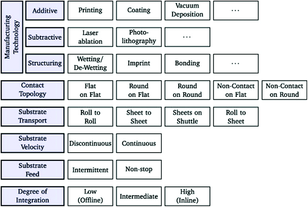 | ||
| Fig. 1 A classification of various manufacturing processes of potential relevance to device fabrication. Reproduced with permission from ref. 6. | ||
Nanomaterials are ideal additive building blocks for additive processes7,8 as they permit precise control over material properties, high purity through synthesis-dependent methods, selective collapse of dimensional symmetry, confinement of carrier wavefunctions,9 and resulting changes in properties, growth methods attuned to dimensionality of such material systems, control of the extent and nature of interconnection between nanomaterials10 that permit different kinds of material aggregation at different length scales, and thus permit the expression of different emergent material properties and device performance.11 The design of material properties is possible through the intelligent use of synthesis and fabrication methods, otherwise it is not accessible without radical changes in the fundamental chemistry of constituent substances, something that is not always possible. Thus, while superficially, aggregation of materials at the length scales of relevant devices is the first apparent benefit of combining additive processes like printing with nanomaterials, the economies of scale in the process, the development of mesoscale properties and unique device architectures12 present an endless variety of choices of device fabrication routes and obviates several processing limitations otherwise inherent in top-down or subtractive manufacturing.13
2. Printing methods
While not strictly classifiable as bottom-up fabrication processes, printing processes (with some exceptions) are additive in nature and thus are similar in spirit to these bottom-up processes at larger length scales. Traditional printing in laboratory research involves the ejection of a (usually) liquid ink out of a cartridge in the form of controllable drops, the impact of the drop on the desired substrate, and its subsequent motion under the joint influence of surface tension interaction with the substrate influencing the initial radially outward motion, evaporation of the solvent comprising the ink, time-dependent viscosity of the variable mass ink system and interaction with the ambient in terms of temperature and humidity.14–16 A slight departure in this process has gained prominence in recent years in the form of three-dimensional printing which involves a layer by layer construction of three-dimensional objects using cross-sections derived from a three-dimensional model of the object, and employing a binder material. It is possible to look at inkjet printing, which is described next, as an exemplar 3D printing process if the ink can be immobilized on the substrate quickly, and added ink preferably deposits new material vertically instead of spreading out horizontally.17 In this section, we will briefly survey two main printing methods – inkjet/3D printing and roll-to-roll printing and related processes. This choice is based on the relative complexity of these two printing processes. Other printing methods like screen printing,18 gravure printing/imprinting,19–21 flexographic printing19,22–24etc. find extensive applications, and are referenced in the remainder of this review as needed. The reader is advised to consult the cited literature on the subject to become familiar with these closely allied processes.2.1. Inkjet printing
Like laser-based direct write methods, such as femtosecond laser ablation,25 and laser decal transfer,26 volatile liquid-based printing methods can employ a variety of materials, depending on the nature of the printing process and what is sought to be printed.14,27 While either solution- or suspension-based inks can be printed, these choices correspond to certain unique features and limitations in actual practice.Solution-based inks, depending upon the volatility of the solvent used and the viscosity of the ink, can provide a simpler and more deterministic print recipe design once the rheological properties of the ink are known and the environment suitably controlled. However, the solubility of the materials sought to be deposited is controlled by the nature of the solvent, temperature, humidity and ink pH. This combination of factors can limit overall weight loading and result in various film non-idealities upon drying, such as cracking upon volume contraction, intrinsic stress and, in extreme cases, peeling off or delamination. An ideal solution-based ink and its deposition process would contain a sufficient loading of the solute and be dried in a manner that preferentially densifies at the substrate–ink interface, thereby avoiding volumetric cracking. In geometric terms, such a process could be triggered to precipitate the solute by exceeding the solubility limits controllably in a localized region of the ink column above the substrate. A temperature gradient between the cartridge printing the ink and the substrate, for instance, could accomplish this task. On the other hand, the use of suspension-based inks, which may involve the use of colloidal suspensions and nanoparticles, permits the ink designer to exceed solubility limits greatly, thereby increasing the weight loading and producing more stable films. However, such suspensions can be unstable and thus have a fixed shelf-life beyond which precipitation and aggregation become appreciable. In both cases, the process designer must contend with the tendency of the printed ink to form ring stains, or central spikes due to capillary28 or Marangoni29 flows during the drying of the ink drop, to different extents.
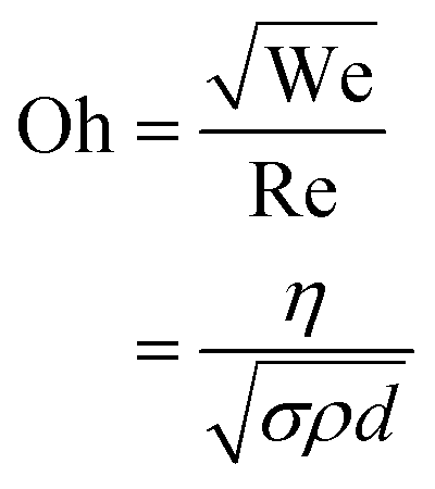
A recently demonstrated direct writing technique exploits the capillary effect in conjunction with a rollerball pen.30,31 In traditional inkjet printing systems based on piezoelectric heads, the feature size that can be printed is closely related to the size of the droplet that can be ejected and surface treatments of substrates.27,32–34 Furthermore, the droplet size is also a strong function of the nozzle diameters. The effect of the jet velocity, v, the orifice diameter, d, the surface tension, σ, and the density of the ink, ρ. We can define the Ohnesorge (Oh) number for a print process as
 | (1) |
While picoliter level volume control is readily attainable using piezoelectric cartridges in conjunction with inkjet printing, the desire to access ever finer feature sizes has resulted in the development of subfemtoliter inkjet printing systems based on electrohydrodynamic (EHD) jet printing.35,36 The pulsing frequency37 is found to exert a strong influence on the formation of ink droplets as exhibited in Fig. 2. The authors37 found that with increasing frequency, the droplets formed reduced in size (and size variability), which would be expected to decrease the size of the minimum feature printed. However, this decrease was accompanied by an increase in the impact velocity of the droplet on the substrate, which in turn is expected to degrade the quality of the print. The placement accuracy of the drop is governed by the width of the jet and the resolution provided by the moving stage.38,39 The diameter of the jet has been found to be proportional to the square root of the nozzle size and inversely proportional to the electric field.40 Earlier studies have indicated that it is possible to access very fine dot-like features (∼240 nm) using EHD-based printing methods.35 There are several reports on line-widths and three dimensional features in the range of 1–20 μm.40–42 Applications of this increasingly popular process include electrospinning of polymers using a direct writing technique.43
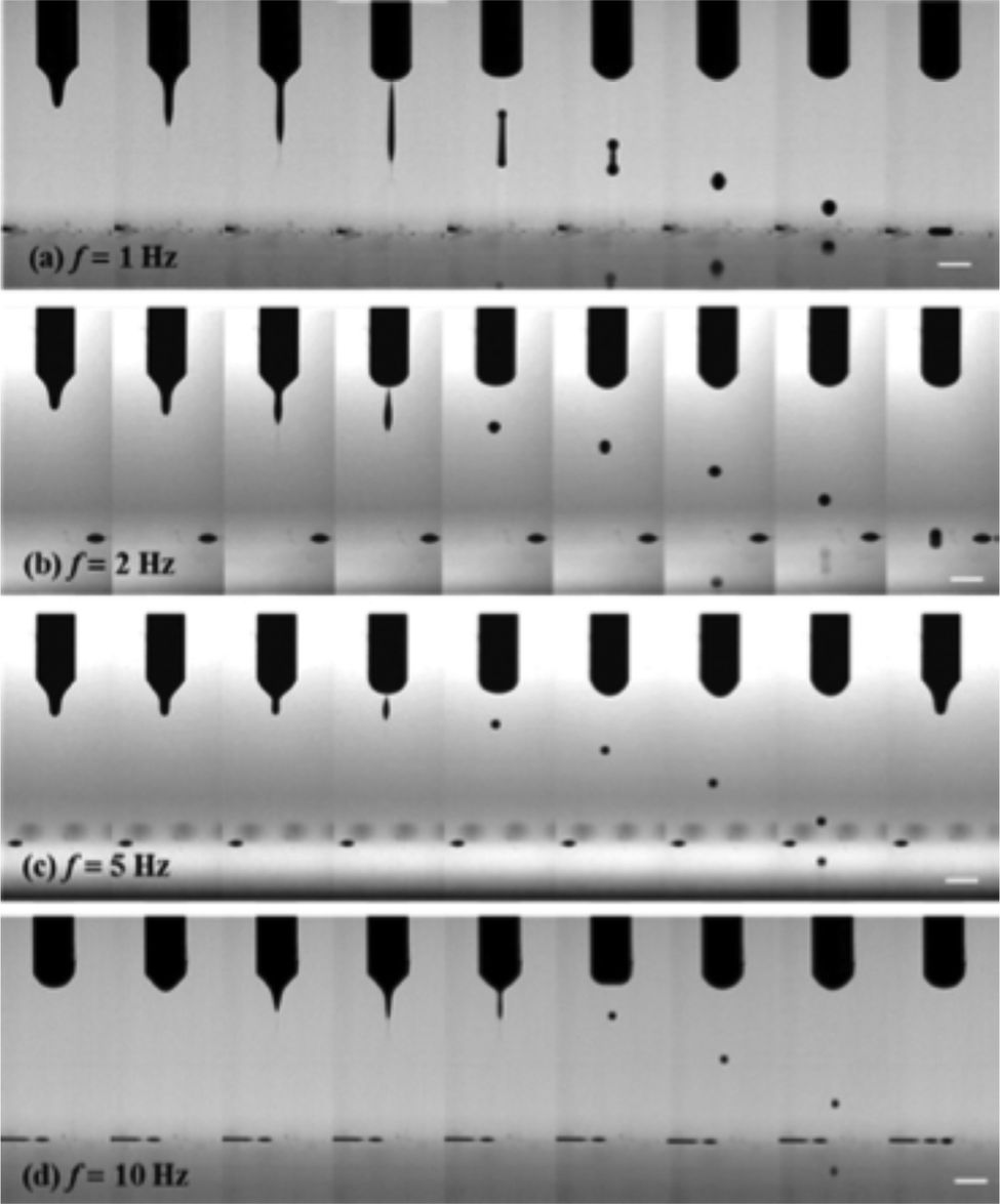 | ||
| Fig. 2 EHD silver ink droplet ejection as a function of frequency. Time interval = 1 ms, scale bar = 1 mm. Reproduced with permission from ref. 44. | ||
Solution-based processes like printing lend themselves naturally to large area deposition of various dissolved species or suspensions. While the performance of solution-deposited devices lags slightly behind devices fabricated using more conventional micro-fabrication methods, the gap in performance has narrowed in recent years.45 This encouraging improvement in device performance has opened up stronger prospects of industrial adoption of printing processes as preferred low-cost fabrication. As a process based on extensive use of solvents which are volatile, or have to be disposed after use, it is essential that the best practices in inkjet printing be informed by our latest understanding of green chemistry.46,47π*–β or Kamlet–Taft plots for solvents are used to systematise the search for solvents depending on the application. However, beyond basicity and polarity, other parameters of a solvent, such as boiling point, viscosity, surface tension, solubility, density, and specific gravity, are also relevant to a print process, as are the mathematical quantities defined in eqn (1). This shrinks the corresponding solution space even further,46 making it a particularly difficult challenge to meet. It is essential to realize that given the sensitivity of printing processes to the choice of the solvent, a resolution of this problem cannot be deferred as an industry-specific problem of little interest to scientists in the lab. In this light, a recent study has explored the use of non-halogenated solvents for large area OLED and OSC applications of polymer printing.48 A new strategy turns the traditional idea of high-boiling point solvents with high solubility on its head by combining a volatile, high solubility solvent with a stable, low solubility solvent.49 The effect of such a choice on the throughput of device fabrication is still unexplored.
If the ink used in an inkjet printing process can be made significantly more viscous or the printed material can otherwise be quickly immobilized on the surface instead of undergoing capillary28 or Marangoni flow,29 material growth occurs preferentially in the vertical direction as opposed to the formation of relatively thin layers. This regime of printing can technically be referred to as 3D printing. In practical 3D printers, binder elements (as in fused deposition modelling) are added to provide the binding force between the material sought to be printed as well as the higher viscosity needed to suppress lateral expansion of the droplet. Though the process is more than 40 years old,50 significant price drops after 2010 and the availability of easy to use software have pushed this technology into teaching, research, and importantly, hobby-craft.51,52 Unsurprisingly, market trends have followed suit.53,54 Due to the rapidly expanding range of applications of conventional printing processes,14,55–57 extensions of the achievements with conventional printing processes have begun to be replicated in the third dimension as well.58 One of the most common applications of 3D printing involves the creation of rapid prototypes that can be used for casting or heat pressing.59 Historically, initial work done by the Evans group on direct inkjet printing involved printing or ceramic-based60,61 and wax-based oxide62 suspensions and 3D growth of vertical walls.63
One of the major disadvantages of 3D printing is the deviation from design lengths due to composition-dependent volumetric changes in the polymer-binder as it dries after the print (bleeding effect). When the size of the printed object reduces, there is a need for more intelligent software that can take the drying properties of the ink into account and design around it.64–67 Contrary to expectations from the historical market response to expiry of patents, such as the fused deposition modeling patent (FDM) which expired in 2009, the more recent expiry of the selective laser sintering patent in January 2014 has not yet led to an exponential growth in open source/hardware solutions corresponding to that technology,68 though one may reasonably expect greater growth in the years to come.
2.2. Roll-to-roll printing
Methods of printing corresponding to the graphics arts industry, such as newsprint, banner and textile printing, are expected to maximize the throughput of large-area flexible device fabrication. While alternatives to it exist,6 a common method used in this context is roll-to-roll (R2R) printing. Such methods are extensively used applications where the production of large area devices is prominent. Growing interest in wearable devices, such as sensors69 integrated into textiles, has further enhanced the potential uses of this process. Applications of roll-to-roll processing include deposition of electrodes,70–73 sensors,74,75 polymer FETs,76 optical films,77 and most importantly, large-area solar cells.19,22,23,78–84 R2R methods can be combined nearly seamlessly with other industrially scaleable processes such as chemical vapour deposition (CVD),85 sputtering,86 and address small feature sizes accessible during UV-imprint87 and nano-imprint88 lithography. Conventional application of the R2R process has involved single thin film deposition of several types of materials. However, as an R2R system can hold more than one roller, sequential deposition of multiple layers has been a main industrial application for a variety of thin (or thick) film processes, and can approach the quality of material deposition available through vacuum deposition processes. The thickness of deposited films is controlled accurately by the gap between the rollers, the rotational speed and the post-deposition annealing steps.It is also possible to transfer a film grown on a metal substrate to a polymer substrate using R2R techniques (Fig. 3). This possibility can be useful in case the deposition temperature of the functional material is beyond the operating limits for the polymeric substrate. For instance, such a transfer printing technique can be used to deposit CVD grown graphene on a polymer substrate.70,87,89 In combination with the use of inorganic nanomaterials directly deposited in an R2R process, this method is expected to save significant cost and time, compared to pure vacuum-based processes.
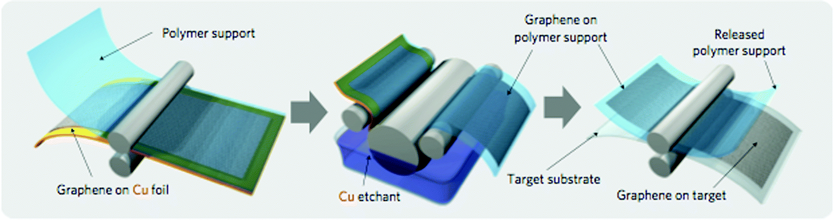 | ||
| Fig. 3 Schematic of the roll-based production of graphene films grown on copper foil. Reproduced with permission from ref. 71. | ||
3. Electrically conductive species
Metal–semiconductor contacts and interconnects permit the combination of devices in larger functional blocks and for us to interact with them. In general, such contacts must permit efficient conduction of charge carriers without adding to the power dissipation and losses. Traditionally, the formation of such conductive layers has involved metallization using processes such as sputtering, evaporation and electron-beam deposition. While these processes are mature and well-tested, and a corresponding library of metal–semiconductor combinations has been developed over the years for a variety of electronic and optoelectronic/photonic devices, these processes are not seamlessly integrated into the solution-processed deposition workflow, and thus can add a significant overhead.Over the last 10–15 years, it has been realized that besides metals, a host of different materials,17,90–94 such as metal nanoparticles, graphene,95 carbon-nanotubes (CNTs),96,97 conductive polymers,98 and transparent conductive oxides,99 can be employed as efficient conductive layers. The formation of suitable metal nanoparticle inks depends on the synthesis of nanoparticles of the correct size range for low sintering temperatures (∼50 nm), the use of surfactants to prevent their agglomeration, stabilization in solution for a reasonable shelf-life (a few months), high weight loading needed for sintering to result in conductively continuous films, high volatility for the functional groups/surfactants when deposited on the substrate to maximize conductivity and the use of low-cost metals such as aluminium and copper, but somehow avoid oxidation and loss of conductivity (especially in the case of aluminium). Ink formulations based on metallic nanoparticles have received extensive attention in recent years and new routes for metallic nanoparticle synthesis have been developed.100–105 Steric stabilization of colloidal nanoparticles is a standard method of stabilization in inks,106 while the use of polymeric functional groups,107 and more recently, antioxidants,108 has proven effective in preventing the oxidation of metallic nanoparticles, especially for copper. Owing to growing indium shortage,109,110 finding alternatives to indium tin oxide (ITO) nanoparticles or ITO substrates (for instance, sputtered ITO on XG glass has a thickness of 145 nm, transmittance of 88% at 550 nm, with a sheet resistance of approximately 20 Ω per sq.) has attracted attention. In that context, other transparent conductive materials111,112 have assumed even greater significance. In the discussion that follows, although several different units for resistivity, conductivity and sheet resistance have been cited from the recent literature, we have collected several of these results together in a consistent set of units in Table 1.
 , and T% = transparency percentage. Some abbreviations: IJP = inkjet printed. SP = screen printed. BP = brush-painted. D = dispensed. DB = doctor bladed. MOD = metallo-organic decomposition. UV = ultraviolet. GO = graphene oxide. RGO = reduced graphene oxide. WGO = weakly oxidized graphene oxide. NGP = nano graphene platelets. NW = nanowires. Curing conditions involve thermal sintering/annealing unless indicated otherwise. Starred numbers (and columns) have been calculated from the provided data
| Method | Material/ref. | d (nm) | Ink chemistry | Curing | ρ (μΩ cm) | C %* | T % |
|---|---|---|---|---|---|---|---|
| IJP | Ag138 | 5–20 | Poly(acrylic) acid/Byk-348/amino methyl propanol | 30 | 43 (120* for 2D) | 4 | 95 |
| IJP | Ag35 | 2–3 | Tetradecane | 130 °C | <25 | >6 | — |
| Thermal imprint/IJP | Ag22 | 216/45 | Water/— | 140/140 °C | 25/1200* | 6.36/0.1 | 82/71 |
| IJP | Ag116 | <150 | Ethanol | 150–300 °C | 21–25 | 8 | — |
| SP | Ag NW156 | 25 700 × 187 | Ethanol | Compaction | 16.47* | 9.65 | — |
| IJP | Ag(MOD)139 | — | — | UV | 15.39* | 10.33 | — |
| IJP | Ag128 | 30–50 | Poly(vinylpyrrolidone)/ethylene glycol/ethanol/glycerol | Photonic flash sintering | 14.31* |
|
— |
| D | Ag136 | 518 × 30 | Ethanol | 200 | 7.4 | 21.5 | — |
| IJP | Ag137 | 11.1 | Poly(acrylic acid) sodium/poly (diallyldimethylammonium chloride) | Chemical sintering | 6.8 | 23.4 | — |
| IJP | Ag114 | <100 | Ethanolamine | 90–120 °C | 6–9 | 27 | — |
| IJP | Ag113 | <20 | Hexylamine/ethyl cellulose | 250 °C | 4.625–9.376 | 34.378 | — |
| IJP | Ag117 | 12.2 | Ethanol | 150–250 °C | 4.54–7.13 | 35.02 | — |
| IJP | Ag37 | 50 | — | Laser | 4.07 | 39.1 | — |
| IJP | Ag107 | 40 | Water/monoethanolamine | 50–180 °C | 3.7–139 | 43.0 | — |
| IJP | Ag130 | 10–20 | Triethylene glycol monoethyl ether | Electrical sintering | 2.7* | 58.9 | — |
| IJP | Ag118 | — | AgNO3/water | Plasma | 1.7 | 93.5 | — |
| IJP/DB | Ag/PEDOT:PSS134 | — | Isopropyl alcohol | 65 °C/225 °C | 170* | 1 | — |
| BP | Ag NW/ITO157 | See ref. | — | ITO:100 °C/Ag: 150 °C | 1090 | — | 79.50 |
| EHD/BP | Ag/ITO158 | 10–25 | Ethanol | 200 °C | 42 | — | 83.72 |
| BP | Ti:In2O3159 | 20–40 | Ethanol | 350–500 °C | ∼3000 | — | 85.48 |
| IJP | Cu@Ag@C/Ag@Cu@C120 | 50 | Water/ethylene glycol (butyl or methyl) ether/isopropanol/Byk-Jet 9132 | — | 227.3–5882.4* | — | — |
| Meyer rod | RGO57 | — | Water/zynol | 650 °C | 13![[thin space (1/6-em)]](https://www.rsc.org/images/entities/char_2009.gif) 425* 425* |
— | 45 |
| IJP | GO151 | — | Water/poly(ethylene glycol) diacrylate | UV | ∼3 × 10¹² | — | — |
| IJP | WGO154 | — | Ethylene glycol/Na dodecylbenzenesulfonate | 100 °C | 2381* | — | — |
| IJP | Graphene153 | — | Ethyl cellulose/cyclohexanone/terpineol | 250 °C | 4000 | — | — |
| IJP | NGP/PANI149 | 40–80 | PANI/surfactant/water | 80 °C | 2.72 × 10⁶* | — | — |
| IJP | SWCNT/RuO2 NW160 | — | Water/Na dodecyl sulfonate | — | 625* | — | 10–80 |
Chen et al.113 have developed a new Ag nanoparticle ink formulation based on a [Ag(dien)](tmhd) complex with hexylamine and ethyl cellulose with a minimum resistivity of ∼60 μΩ cm at a sintering temperature of 150 °C. A lower resistivity was reported by Tao et al.114 who used a metallo-organic ink with ethanolamine as an additive and various aldehyde-based reducing agents to produce conductive films of resistivity values between 6 and 9 μΩ cm. Shen et al.107 have developed poly(acrylic acid) coated silver nanoparticles which exhibit long-term stability and a resistivity of 3.7 μΩ cm with a sintering temperature of 180 °C. Molina-Lopez et al.115 used a sintering temperature of 150 °C for their comb-like printed silver contacts for a humidity sensor. Rivadeneyra et al.116 used a similar structure on the polyimide substrate, but with a longer sintering step at 120 °C. An even lower sintering temperature (∼100 °C) was used by Jung et al.117 by reducing the weight percentage of oleylamine through a ligand-exchange reaction with acetic acid. Bromberg et al.118 used a plasma process (at 900 W) with printed silver nitrate ink to produce a resistivity of 1.7 × 10⁻⁸ Ω m, comparable to the resistivity of bulk silver. The process had a maximal substrate temperature of 75 °C, which makes it attractive as a deposition technique on low-cost substrates. Abulikemu et al.119 have carried out a reactive inkjet synthesis of gold nanoparticles (size ∼8 nm) at 120 °C. Nanoparticles of greater material complexity (bimetal@carbon core–shell and metal@carbon) have been synthesized using reaction under autogenic pressure at elevated temperatures (RAPET) to produce conductivities of printed lines that range from 170 to 4400 S cm−1.120 Kang et al.30 have developed a printed nano-floating-gate memory device based on different types of metallic nanoparticles.
The use of metallic nanoparticles requires post-print sintering of the printed layers to form electrically continuous and highly conductive layers, as exemplified in the ensuing discussion. While the melting points of metals like Al, Ag, Cu and Au are much higher than the highest tolerable temperatures for most flexible substrates, sintering of nanoparticles occurs at a much lower temperature in the case of thermal sintering.
This feature can be intuitively understood as a thermodynamic effect arising from the reduction of the total surface energy,121,122
| Δ(γS) = SΔ(γ) + γΔ(S) | (2) |
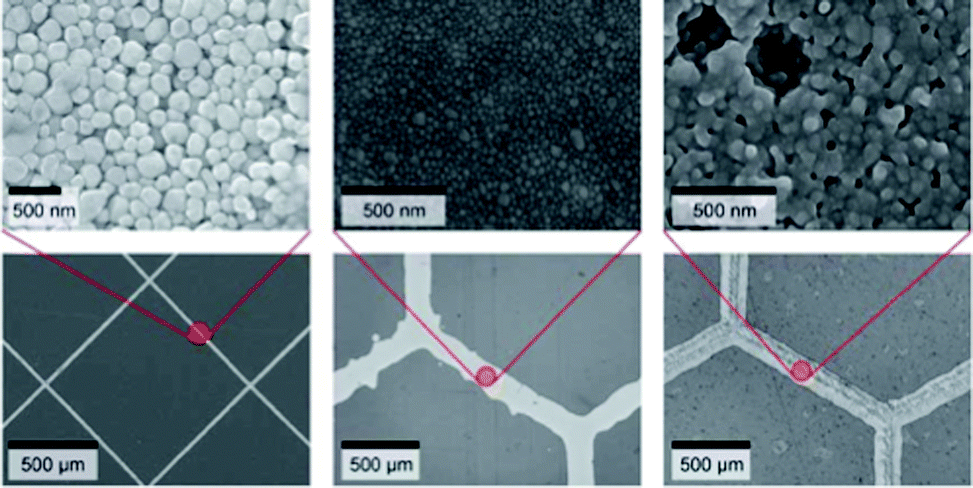 | ||
| Fig. 4 SEM images for nanoparticles for three different silver electrodes and their corresponding optical images. The grid on the left is prepared using thermal imprinting, the one in the middle using inkjet printing, and the one on right using flexographic printing. Reproduced with permission from ref. 22. | ||
3.1. Alternative conductive materials
The aforementioned challenging requirements for metallic nanoparticles have prompted researchers to consider alternatives to metallic nanoparticles, such as CNTs and graphene.140,141 The high aspect ratio of CNTs coupled with van der Waals interactions between them usually leads to the formation of bunches of CNTs and eventual clogging of printheads.96 A very similar effect occurs in the case of graphene solutions, whereby an inter-flake interaction between exfoliated graphene flakes leads to the formation of sandwiches of graphene, which in turn makes it necessary to functionalize graphene to reduce such interactions.142,143 Recent work on non-covalent functionalization of graphene has increased the prospects of high weight loading of graphene inks.144Transparent conducting oxides and hybrid materials based on them are yet another set of promising materials for conductive layers, especially for solar cells.145–148 Doped binary and ternary oxides permit a fine-tuning of resistivity and toxicity.111 Alternatives to conductive oxides include graphene based materials as discussed above. Wang et al.57 used a printable aqueous graphene oxide (GO) ink using a non-ionic surfactant. When coated on a flexible glass, and subjected to a 650 °C anneal, the reduced graphene oxide (RGO) film showed a transmittance of 45% at 550 nm and a sheet resistance of 5370 Ω per sq.
Xu et al.149 have inkjet printed a composite nano graphene platelet (NGP)/polyaniline (PANI) ink to produce layers with a conductivity of 3.67 S cm−1 for supercapacitors with an energy density of 2.4 Wh kg−1. Chen et al.150 have screen-printed a composite layer consisting of Al nanoparticles and wrinkle-like graphene sheets to achieve a 7.2% enhancement in the photocurrent of a silicon solar cell. Giardi et al.151 have used a graphene oxide (GO)/acrylic (poly(ethylene glycol)) composite ink in conjunction with UV-curing to demonstrate a non-thermal route. The thermal reduction of GO represents an increasingly popular deposition route for graphene.152 Secor et al.153 directly printed solution-phase exfoliated graphene to obtain a resistivity of 4 mΩ cm after a 250 °C anneal for 30 min. Much higher conductivities (∼420 S cm−1) were achieved by Su et al.154 with weakly oxidized GO and used in a single-wall CNT FET exhibiting a mobility of 8 cm2 (V s)−1. Organic field-effect transistor (OFET) performance enhancement with the use of GO on a silicon oxide substrate with triisopropylsilylethynyl (TIPS) pentacene155 with printed silver drain and source contacts has recently been reported and attributed to enhanced grain size.
The use of different nanomaterial systems together in the same device, either as separate components or as hybrid materials, has found applications in recent years. Xie et al.161 used inkjet printed silver contacts and spray coated functionalized multi-wall CNTs (MWCNTs) to demonstrate a humidity sensor on paper. Jeong et al.158 have used an invisible silver grid in combination with an ITO nanoparticle layer as a transparent contact. They have also demonstrated a variant with silver nanowires157 and titanium-doped indium oxide159 with brush painting. The high surface to volume ratio of CNTs (with RuO2 nanowires) has found applications in flexible supercapacitors160 and in electrothermal applications involving effective Joule heating (with graphene-based materials).162 Hurch et al.163 have used inkjet printing in two different ways to pattern a channel for chemical vapor deposited (CVD) graphene and the conductive contacts while transferring the print-defined pattern from a copper foil to a different substrate. This hybrid process is exhibited in Fig. 5. Transfer techniques have also been used for n-OFETs with gold electrodes164 to reduce the inverse subthreshold slope and increase the linear region mobility by 200%, a performance comparable to low-work function materials like Al and Ca (which are unstable in air).165
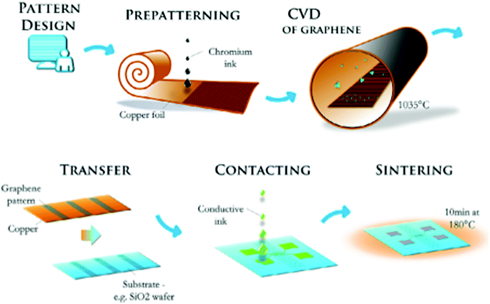 | ||
| Fig. 5 A process employing inkjet print patterning, deposition and pattern transfer to produce graphene FETs. Reproduced with permission from ref. 163. | ||
3.2. Low-cost substrates
Low-cost substrates like paper using pulp and nanofibrillated fibers have attracted attention as alternative flexible substrates. A recent comparative study166 using sputtered gold, silver nanoparticle ink and particle-free metallo-organic silver ink has yielded very low resistivities. In another report,167 a recyclable paper substrate was also used to fabricate an electrochemical analysis platform using printed gold for working and counter electrodes, while a printed silver stripe formed the basis of the reference electrode. Huang et al.156 have developed a printing-filtration-press (PFP) technique for the mass production of flexible bending-resistant paper-based circuits with a conductivity of ∼61 000 S cm−1, using silver nanowires. They have demonstrated this technique for radio frequency identification (RFID) tags and cellphone cables. Inkjet printed antenna structures on a variety of substrates and in a variety of shapes using direct and catalyst printing27,168–170 have been demonstrated. Using a variety of conductive nanomaterials discussed above, given the wide applicability of RFID-based devices,171,172 there have been reports of printed RFID-based sensors,173,174 gas sensors,175,176 biomedical sensor nodes,177 hemispherical antennas (Fig. 6),169 and microfluidic RFID-enabled platforms for wireless lab-on-chip applications.178 Paper-based bio-sensors have found a special niche as disposable, low-cost and portable sensors for protein analysis, lab-on-chip applications, and environmental toxins.179 Shemelya et al.180 used copper wires as a capacitive sensor embedded in printed polycarbonate with a sensitivity better than 0.1%. Cheap force sensors can also be fabricated using printing methods.181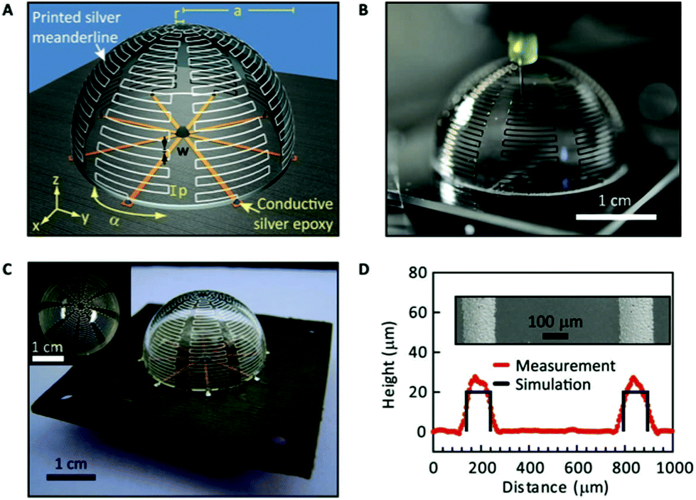 | ||
| Fig. 6 Conformal direct printing of an electrically small antenna, with optical images and optical profilometry results. Reproduced with permission from ref. 169. | ||
With the use of low-cost substrates like plastic and paper and other flexible substrates, it is also important to consider the mechanical stability of the devices, in response to flexion and bending. Repeated stress can lead to strain in various layers, delamination and device failure. Studies that test for stability towards repeated strain are thus essential before commercialization of any flexible devices.182–184
4. Semiconducting and insulating species
While conductive layers can be inorganic, such as for transparent conductive oxides, in this section, we briefly survey the current state of art of printing of inorganic nanoparticles as functional components of different electronic, and intriguingly, non-electronic devices. Inorganic nanoparticles offer prospects for or current applications in quantum-dot based light-emitting diodes (QDLEDs),185–187 organic–inorganic hybrid material based LEDs,188,189 solar cells,190–192 gas sensors,193 photovoltaics194–196 and biosensors.197 We have briefly discussed the sintering of nanoparticles in section 3. In the discussion that follows, it is implicitly assumed that sintering of inorganic nanoparticles91,198 is governed by similar physics.There has been a resurgence in research interest in dye-sensitized solar cells due to advances in materials, material deposition methods, and solid phase electrolytes. Screen printed190,191,199–202 and inkjet printed199,203 TiO2 nanoparticles and other nanosystems like titanium oxide nanobundles204 are common photoelectrodes for organic and dye-sensitized solar cells. Conventional room temperature methods of forming TiO2 paste involve suspending the nanopowder in ethanol, sonication and adding titanium tetraisopropoxide (TTIP) as a hydrolyzing agent to form a stable and uniform suspension.205 Recently, Dar et al.206 demonstrated a microwave-based approach to synthesize anatase titania nanomaterials in two different size regimes for functionally different parts of a dye-sensitized solar cell exhibiting an efficiency of 6.5%. Titania nanomaterials can be deposited using nanomaterials of different dimensionality and size using screen printing.207 Chang et al.208 doped TiO2 with up-converting nanoparticles to form TiO2/NaYF4:Yb3+, Er3+ nano-heterostructures, which were fabricated using screen printing of the resulting paste. They found that the samples with the up-converting nanoparticles showed a 17% improvement over samples that did not. Other reported methods of increasing the efficiency of the photoanodes in solar cells involve tungsten doping.209
Besides titanium oxide, other viable species such as ZnO192,210 and BiVO4211 have also attracted interest in recent years. Kwon et al.212 showed direct selective growth of ZnO nanowires using a zinc acetate ink precursor, and demonstrated field-effect transistors and UV photodetectors using this fabrication method. Printing of composite ZnO–TiO2 nanoparticles and screen printing of TiO2 paste on to ZnO microrod arrays grown on glass213 are methods of producing a complex nanocomposite. In situ growth of MgO and ZnO films through printing of acetate solutions214 and self-organized growth of CuO hollow spheres are examples of alternatives to pre-synthesis and subsequent deposition.215 Other possible composite components include graphene216 which have been used to fabricate dye-sensitized solar cells. Krebs et al.82 have demonstrated a complete R2R process involving ZnO nanoparticles (Fig. 7).
 | ||
| Fig. 7 The slot-die coating of ZnO nanoparticles (left), P3HT:PCBM (middle) and PEDOT:PSS (right). Wet films on the top and dried ones are shown below. Reproduced with permission from ref. 82. | ||
Chalcogenide material systems have attracted significant interest due to the wide variety of n- and p-type materials available with differing mobilities, and synthetic methods for large scale production of nanoparticles have been developed.217 More complicated nanomaterial systems218 can be created with in situ growth of PbS nanoparticles on ZnO nanowires using a printing-based approach. Bronstein et al.219 have used CdSe/CdS seeded nanorods as a tunable lumophore with embedded, transfer-printed crystalline Si solar cells. The resulting area of the luminescent concentrators is 5000 times the area of the solar cell. Nguyen et al.220 have printed (using a doctor blade method) Cu(In,Ga)S2 nanoparticles and selenized to form Cu(In,Ga)Se2 (CIGS) solar cells. After annealing and etching with KCN, they found improved photovoltaic performance. Application of rapid thermal processing methods221 can help speed up the fabrication of CIGS solar cells even further.
Boulfrad et al.222 have used perovskite-based nanomaterials to demonstrate scalable anodes for solid oxide fuel and electrolytic cells. They doped x wt% Ce0.9 Gd0.1O2−δ (CGO) into (La0.75Sr0.25)0.97Cr0.5Mn0.5O3 (LSCM) and coated it with y% nickel oxide or nickel nitrate to prepare a screen printable ink in an organic solvent for the anode. An ink comprised of (La0.8Sr0.2)0.95MnO3 (LSM) was prepared for the cathode. Three compositions – A(x = 15, y = 0), B(x = 15, y = 5, source = NiO) and C(x = 15, y = 5, source = Ni(NO3)3) – were tested. The results of impedance measurements carried out at two different temperatures, with a fuel source: H2 + 3% water vapour, are shown in Fig. 8.
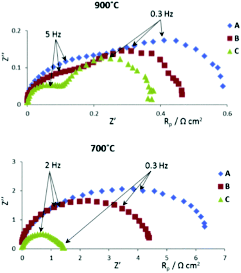 | ||
| Fig. 8 Impedance diagrams for three different anode compositions under 50 ml min−1 pure wet hydrogen gas flow. Reproduced with permission from ref. 222. | ||
Piezoelectrics like lead zirconate titanate (PZT) form the basis of functional layers involving the interplay of mechanical movement and charge state, and advances made in the synthesis of suitable inks223,224 and printing processes225 are significant. Wei et al.226 reported the design, fabrication and testing of a planar valveless micropump screen printed on to a polyimide substrate. They achieved a maximum flow rate of 38 μl min−1 using a drive frequency of 3 kHz.
While organic and polymeric species have found applications as diverse as OLEDs,227–230 piezoelectric actuators,231 and ferroelectric memories,232 pioneering studies on reinforced composites employing thermoplastic polymers,233,234 and solar cells,19,235–238 and the printing of polymer- and organic semiconductor based nanoparticles have revealed them to be functional materials with several applications. To promote the adhesion of polymer species on common substrates, variants of printing processes like polymer grafting239 have been developed. Interestingly, inkjet printing of molten precursors has been used to produce polymers like nylon 6.240 Being soft materials, polymer nanoparticles are subject to a change in their properties in response to mechanical stress.241 Given the presence of conjugated carbon–carbon bonds, it is not surprising that many polymer nanomaterial systems are good potential candidates for biosensing applications. Weng et al.242 have demonstrated a fully-printed polypyrrole (PPy)-based biosensor consisting of inkjet printed biomaterials composed of PPy-enzyme formulations deposited on to screen printed carbon electrodes. They found a peroxide detection threshold value of 10 μM and a higher threshold for glucose, 1 mM. Hibbard et al.243 have used printed polyaniline (PANI) nanoparticles to create an ammonia sensor for human breath. Several other sensor applications involving PANI have been reported and reviewed.244 Eissa et al.245 have used microcontact printing to deposit epoxy-functionalized magnetic colloidal particles for specific antigen detection. Akagi et al.246 have used inkjet printing of a layer-by-layer poly(lactide) stereocomplex as a drug vector with up to 100 wt% loading. The Citterio group247 has created an inkjet printed colorimetric sensor array for the discrimination of volatile primary amines through their sensitivity to the polarity of the species. Tang and Feng248 have reviewed conjugated polymer luminescent nanoparticles for imaging and therapeutic applications.
5. Biological and pharmaceutical species
Biological tissue differs in essential ways from the materials discussed so far. The chemical composition largely consists of the elements of life – C, H, N, O, P and S, in addition to elements like Ca which form the bulk of bone tissue, in the two major components organic collagen and inorganic hydroxyapatite (Ca10(PO4)6(OH)2). Bone growth occurs as a result of mineralization involving osteoblasts, which are bone-forming cells within the human body. Due to wasting diseases like polio or traumatic loss of bone tissue, it sometimes becomes necessary to replace bone tissue. While the subject of bone implants and reconstruction is beyond the scope of this review, it should be noted that the use of nanomaterials has been known to enhance in vitro and in vivo osteoblast function, which indicates that the process of integration of implants (osseointegration) is augmented by the use of nanostructured metals, ceramics, polymers and composites.249Thus, it should not be surprising that the first attempts to employ printing (especially 3D printing) in biotechnology involved bone tissue engineering (BTE). Powder-based nanomaterials like calcium phosphates250 have been used for their superior biocompatibility and mechanical strength.44,251–255 3D printing has been used to fabricate scaffolds,256–258 followed by their installation on to damaged bone. During this process, polymers are used to bind calcium phosphate powder and then heat treated to form a permanent connection after the print.259–262 The organic component of natural bone tissue, collagen, has also been used in 3D printing.263–265 Besides being bone replacement tissue, 3D printing is also critical to the fabrication of biomedical prototypes as a diagnostic aid or for the planning of bone/tissue surgery as shown in Fig. 9.
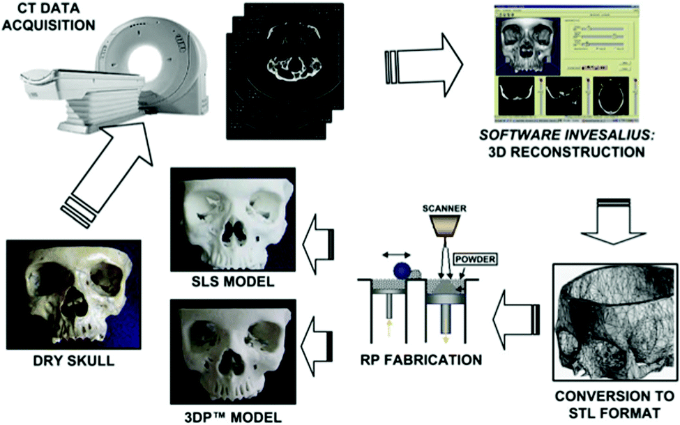 | ||
| Fig. 9 Steps involved in prototyping a human skull using 3D printing methods (selective laser sintering). Reproduced with permission from ref. 266. | ||
As is evident from the work cited above, most of the work involving 3D printing has focused on the design of bone scaffolds as they serve as a three-dimensional template for initial cell growth.44,254 However, a scaffold must have a highly porous structure257,258 that permits cell migration and nutrition. A pore size suitable for this purpose is estimated to be in the range of 50–1000 μm for effective bone regeneration.260
Three-dimensional networks consisting of hydrophilic polymer chains with high water content, or hydrogels,269 have been deposited using printing, especially for bionic organs and cybernetics.270–275Fig. 10 shows a functional bionic ear that is mechanically and acoustically similar to a human ear.267 There have been reports of the synthesis of hydrogels from natural and synthetic sources and their use in drug delivery, stem cells, and cancer research.276–281 Due to the mechanical limitations of natural hydrogels such as collagen, chitosan, hyaluronic acid (HA), gelatin, elastin, etc., these have been replaced by synthetic hydrogels such as poly(ethylene glycol) (PEG), poly(vinyl alcohol) (PVA), and poly(acrylamide) (PAM) in several recent studies.54,260 These hydrogels have been used as an artificial extracellular matrix supporting the regeneration of various tissues. Hydrogels can be freely printed as they do not generally give rise to nozzle clogging.282
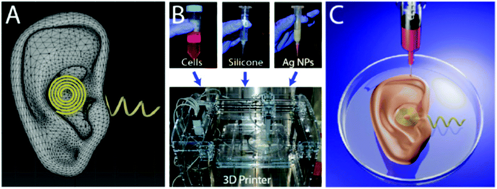 | ||
| Fig. 10 Three-dimensional interweaving of biology and electronics via additive processes. The functional materials used include chondrocytes, silicone and silver nanoparticle ink fused silicone. Reproduced with permission from ref. 267. | ||
Auxetic structures (Fig. 11)268 occur naturally in cubic elemental metals, α-cristobalite, biological tissues (for instance, in feline skin). Polyurethane foams exhibit a similar behaviour with tri-axial volumetric compression and relaxation. Such a structure can be replicated using 3D printing methods and used in the creation of complex structures with emergent properties, such as metamaterials for a suitable wavelength.
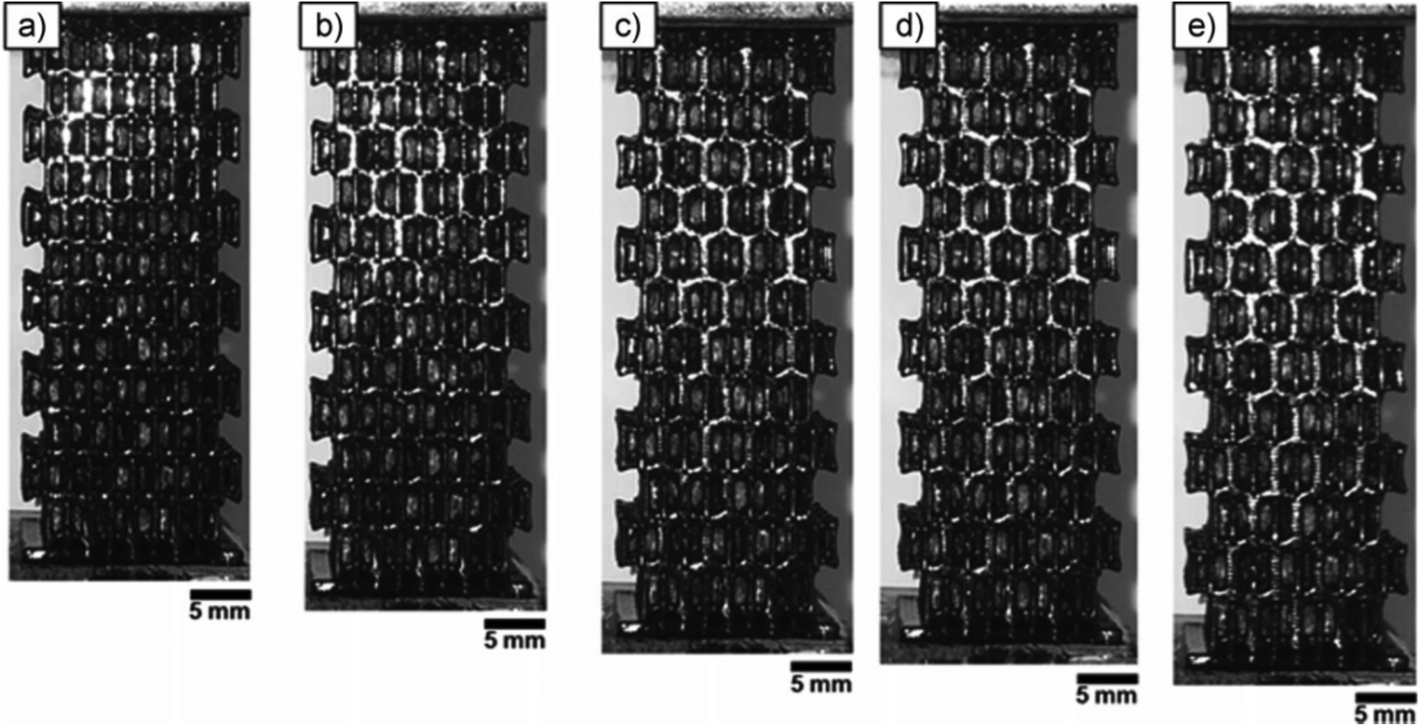 | ||
| Fig. 11 Sequence of strain induced structural changes in a 3D printed auxetic foam from (a) re-entrant lattice to (e) honeycomb structure. The strains are as follows: (a) 0%, (b) 5%, (c) 12%, (d) 14%, and (e) 19%. Reproduced with permission from ref. 268. | ||
6. Conclusions
We started this review article with a discussion of additive processes and nanomaterial systems with an argument that the class of processes and the class of materials were well suited to be combined to fabricate new kinds of devices with performance that is not achievable with conventional subtractive processes acting upon bulk materials. While not exhaustive, in this review, we have attempted to provide a fairly wide-ranging and nearly feature-complete view of the field. It is quite apparent that for several classes of devices, the performance difference between the vacuum deposition and the solution-processed printed version is beginning to shrink or even disappear altogether.Subtractively fabricated nanosystems under vacuum already provide very high efficiency solar cells (III–V multi-junction concentrators), and very short channel FETs with acceptable transfer characteristics, three-dimensional gated structures etc. However, the dimensional limits of subtractive processes are now beginning to show themselves. For the first time in over four decades, Moore's law is no longer expected to double the number of transistors on a chip every 18 months. Such a situation suggests quite naturally the fabrication of devices starting from the other length extreme – atoms and molecules.
However, nanomaterials possess a high surface to volume ratio, which results in a stronger coupling between material properties and processing parameters, such as solutions, impurities in the ambient, and interaction with other nanomaterials. While the latter interaction is often physically desirable in the design of materials with emergent properties, unintentional or unforeseen interactions modify the physical behaviour of these nanosystems in unpredictable ways and are responsible for some of the performance degradations seen in non-vacuum processes. While the removal of all unintentional chemistry at the nanoscale is not possible for solution-processes, the active addition of chemistry, in the form of functionalized nanoparticles that are more stable in solution than bare nanoparticles, suggests itself to be one possible route forward.
It will be interesting to examine the effect of applying biological principles and self-assembly to create new material properties, while combining nanoscale chemistry with a combination of many different printing processes to access different length scales of material organization. A tantalizing possibility that exists involves the use of a purely synthetic approach coupled with printing processes to achieve all device architectures currently accessible through expensive, low-throughput methods of device fabrication, such as e-beam lithography, focussed ion beam, atomic layer deposition etc. For achieving future nanoscale devices that meet our ever more demanding specifications, it is essential that this possibility be met to achieve the necessary industrial scale-up.
References
- S. A. Campbell, The science and engineering of microelectronic fabrication, Oxford University Press, 2nd edn, 2001 Search PubMed.
- R. G. Hobbs, N. Petkov and J. D. Holmes, Chem. Mater., 2012, 24, 1975–1991 CrossRef CAS.
- M. Shimomura and T. Sawadaishi, Curr. Opin. Colloid Interface Sci., 2001, 6, 11–16 CrossRef CAS.
- N. C. Seeman and A. M. Belcher, Proc. Natl. Acad. Sci. U. S. A., 2002, 99, 6451–6455 CrossRef PubMed.
- W. Lu and C. M. Lieber, Nat. Mater., 2007, 6, 841–850 CrossRef CAS PubMed.
- J. Willmann, D. Stocker and E. Dörsam, Org. Electron., 2014, 15, 1631–1640 CrossRef CAS PubMed.
- T. A. Campbell and O. S. Ivanova, Nano Today, 2013, 8, 119–120 CrossRef CAS PubMed.
- H. J. Gysling, Curr. Opin. Colloid Interface Sci., 2014, 19, 155–162 CrossRef CAS PubMed.
- M. Singh, V. Ranjan and V. A. Singh, Int. J. Mod. Phys. B, 2000, 14, 1753–1765 CrossRef CAS.
- A. M. Elliott, O. S. Ivanova, C. B. Williams and T. A. Campbell, Adv. Eng. Mater., 2013, 15, 903–907 CAS.
- P. Wang, J. Ma, F. Shi, Y. Ma, Z. Wang and X. Zhao, Ind. Eng. Chem. Res., 2013, 52, 10355–10363 CrossRef CAS.
- F. Zhu, N. P. Macdonald, J. M. Cooper and D. Wlodkowic, Micro/Nano Mater. Devices Syst., 2013, 8923, 892344 Search PubMed.
- O. Ivanova, C. Williams and T. Campbell, Rapid Prototyping J., 2013, 19, 353–364 CrossRef.
- M. Singh, H. M. Haverinen, P. Dhagat and G. E. Jabbour, Adv. Mater., 2010, 22, 673–685 CrossRef CAS PubMed.
- J. G. Korvink, P. J. Smith and D.-Y. Shin, Inkjet-based Micromanufacturing, John Wiley & Sons, 2012 Search PubMed.
- P. J. Smith and A. Morrin, J. Mater. Chem., 2012, 22, 10965–10970 RSC.
- A. Kamyshny and S. Magdassi, Small, 2014, 10, 3515–3535 CrossRef CAS.
- H.-W. Lin, C.-P. Chang, W.-H. Hwu and M.-D. Ger, J. Mater. Process. Technol., 2008, 197, 284–291 CrossRef CAS PubMed.
- F. C. Krebs, Sol. Energy Mater. Sol. Cells, 2009, 93, 394–412 CrossRef PubMed.
- D.-Y. Shin, M. Jung and S. Chun, J. Mater. Chem., 2012, 22, 11755–11764 RSC.
- J. G. Ok, H. S. Youn, M. K. Kwak, K.-T. Lee, Y. J. Shin, L. J. Guo, A. Greenwald and Y. Liu, Appl. Phys. Lett., 2012, 101, 223102 CrossRef PubMed.
- J.-S. Yu, I. Kim, J.-S. Kim, J. Jo, T. T. Larsen-Olsen, R. R. Søndergaard, M. Hösel, D. Angmo, M. Jørgensen and F. C. Krebs, Nanoscale, 2012, 4, 6032–6040 RSC.
- R. R. Søndergaard, M. Hösel and F. C. Krebs, J. Polym. Sci., Part B: Polym. Phys., 2013, 51, 16–34 CrossRef.
- M. Wessling, L. G. Morcillo and S. Abdu, Sci. Rep., 2014, 4, 4294 CAS.
- X. Wang, P. Lu, N. Dai, C. Liao, Y. Wang, Q. Zheng, X. Guo and Q. Zhang, J. Micromech. Microeng., 2007, 17, 1307 CrossRef CAS.
- A. Piqué, R. C. Y. Auyeung, H. Kim, K. M. Metkus and S. A. Mathews, J. Laser Micro/Nanoeng., 2008, 3, 163–169 CrossRef.
- M. Singh, H. M. Haverinen, Y. Yoshioka and G. E. Jabbour, in Active Electronics, ed. I. M. Hutchings and G. Martin, John Wiley & Sons, Ltd, 2012, pp. 207–235 Search PubMed.
- R. D. Deegan, O. Bakajin, T. F. Dupont, G. Huber, S. R. Nagel and T. A. Witten, Nature, 1997, 389, 827–829 CrossRef CAS PubMed.
- D. Pesach and A. Marmur, Langmuir, 1987, 3, 519–524 CrossRef.
- M. Kang, K.-J. Baeg, D. Khim, Y.-Y. Noh and D.-Y. Kim, Adv. Funct. Mater., 2013, 23, 3503–3512 CrossRef CAS.
- J.-Y. Lee, B. Choi, B. Wu and M. Lee, Biofabrication, 2013, 5, 045003 CrossRef PubMed.
- H. Y. Park, B. J. Kang, D. Lee and J. H. Oh, Thin Solid Films, 2013, 546, 162–166 CrossRef CAS PubMed.
- J. Lessing, A. C. Glavan, S. B. Walker, C. Keplinger, J. A. Lewis and G. M. Whitesides, Adv. Mater., 2014, 26, 4677–4682 CrossRef PubMed.
- H. Meier, U. Löffelmann, D. Mager, P. J. Smith and J. G. Korvink, Physica Status Solidi A, 2009, 206, 1626–1630 CrossRef CAS.
- J.-U. Park, M. Hardy, S. J. Kang, K. Barton, K. Adair, D. k. Mukhopadhyay, C. Y. Lee, M. S. Strano, A. G. Alleyne, J. G. Georgiadis, P. M. Ferreira and J. A. Rogers, Nat. Mater., 2007, 6, 782–789 CrossRef CAS PubMed.
- T. Sekitani, Y. Noguchi, U. Zschieschang, H. Klauk and T. Someya, Proc. Natl. Acad. Sci. U. S. A., 2008, 105, 4976–4980 CrossRef CAS PubMed.
- D. G. Lee, D. K. Kim, Y. J. Moon and S.-J. Moon, Nanotechnology, 2013, 24, 265702 CrossRef CAS PubMed.
- S. J. P. Kress, P. Richner, S. V. Jayanti, P. Galliker, D. K. Kim, D. Poulikakos and D. J. Norris, Nano Lett., 2014, 14, 5827–5833 CrossRef CAS PubMed.
- D. Engstrom, B. Porter, M. Pacios and H. Bhaskaran, J. Mater. Res., 2014, 29, 1792–1816 CrossRef CAS.
- H. K. Choi, J.-U. Park, O. O. Park, P. M. Ferreira, J. G. Georgiadis and J. A. Rogers, Appl. Phys. Lett., 2008, 92, 123109 CrossRef PubMed.
- K. Rahman, K. Ali, N. M. Muhammad, M.-t. Hyun and K.-h. Choi, Appl. Phys. A, 2013, 111, 593–600 CrossRef CAS.
- Y. Han, C. Wei and J. Dong, Manuf. Lett., 2014, 2, 96–99 CrossRef PubMed.
- P. Huang, D. Deng and Y. Chen, ASME 2013 International Mechanical Engineering Congress and Exposition, 2013, 2A, V02AT02A056.
- I. Lee, W.-K. Oh and J. Jang, J. Hazard. Mater., 2013, 252–253, 186–191 CrossRef CAS PubMed.
- L. Shaw and Z. Bao, Isr. J. Chem., 2014, 54, 496–512 CrossRef.
- P. G. Jessop, Green Chem., 2011, 13, 1391–1398 RSC.
- L. Moity, V. Molinier, A. Benazzouz, R. Barone, P. Marion and J.-M. Aubry, Green Chem., 2013, 16, 146–160 RSC.
- T. M. Eggenhuisen, M. J. Coenen, T. W. Slaats, H. Gorter, J. Sweelssen and P. Groen, NIP Digit. Fabr. Conf., 2013, 2013, 203–205 Search PubMed.
- G.-H. Lim, J.-M. Zhuo, L.-Y. Wong, S.-J. Chua, L.-L. Chua and P. K. H. Ho, Org. Electron., 2014, 15, 449–460 CrossRef CAS PubMed.
- C. Hull, Apparatus for production of three-dimensional objects by stereolithography, Google Patents, 1986 Search PubMed.
- D. Velenis, M. Stucchi, E. Marinissen, B. Swinnen and E. Beyne, IEEE International Conference on 3D System Integration,. 3DIC 2009, 2009, pp. 1–5.
- B. C. Gross, J. L. Erkal, S. Y. Lockwood, C. Chen and D. M. Spence, Anal. Chem., 2014, 86, 3240–3253 CrossRef CAS PubMed.
- M. Eisenberg, Int. J. Child-Comput. Interact., 2013, 1, 7–13 CrossRef PubMed.
- P. Zorlutuna, N. Annabi, G. Camci-Unal, M. Nikkhah, J. M. Cha, J. W. Nichol, A. Manbachi, H. Bae, S. Chen and A. Khademhosseini, Adv. Mater., 2012, 24, 1782–1804 CrossRef CAS PubMed.
- H. Kang, J. Lee, S. Jung, K. Yu, S. Kwon, S. Hong, S. Kee, S. Lee, D. Kim and K. Lee, Nanoscale, 2013, 5, 11587–11591 RSC.
- D. Zopes, R. von Hagen, R. Müller, R. Fiz and S. Mathur, Nanoscale, 2010, 2, 2091 RSC.
- J. Wang, Z. Fang, H. Zhu, B. Gao, S. Garner, P. Cimo, Z. Barcikowski, A. Mignerey and L. Hu, Thin Solid Films, 2014, 556, 13–17 CrossRef CAS PubMed.
- Y. Zhang and J. R. G. Evans, J. Colloid Interface Sci., 2013, 395, 11–17 CrossRef CAS PubMed.
- C. Polzin, S. Spath and H. Seitz, Rapid Prototyping J., 2013, 19, 37–43 CrossRef.
- W. D. Teng, M. J. Edirisinghe and J. R. G. Evans, J. Am. Ceram. Soc., 1997, 80, 486–494 CrossRef CAS PubMed.
- M. Mott, J.-H. Song and J. R. G. Evans, J. Am. Ceram. Soc., 1999, 82, 1653–1658 CrossRef CAS PubMed.
- K. A. M. Seerden, N. Reis, J. R. G. Evans, P. S. Grant, J. W. Halloran and B. Derby, J. Am. Ceram. Soc., 2001, 84, 2514–2520 CrossRef CAS PubMed.
- X. Zhao, J. R. G. Evans, M. J. Edirisinghe and J.-H. Song, J. Am. Ceram. Soc., 2002, 85, 2113–2115 CrossRef CAS PubMed.
- J. Hiller and H. Lipson, Rapid Prototyping J., 2009, 15, 137–149 CrossRef.
- W. Wang, T. Y. Wang, Z. Yang, L. Liu, X. Tong, W. Tong, J. Deng, F. Chen and X. Liu, ACM Trans. Graph., 2013, 32, 177 Search PubMed.
- Z. Kappassov, Y. Khassanov, A. Saudabayev, A. Shintemirov and H. Varol, 2013 IEEE International Conference on Mechatronics and Automation (ICMA), 2013, pp. 1697–1702.
- J. Gonzalez-Gomez, A. Valero-Gomez, A. Prieto-Moreno and M. Abderrahim, in A New Open Source 3D-Printable Mobile Robotic Platform for Education, ed. U. Rückert, S. Joaquin and W. Felix, Springer, Berlin, Heidelberg, 2012, pp. 49–62 Search PubMed.
- J. Robinson, Expiring patents were supposed to boost the 3D printing market. They haven't, 2014, http://pando.com/2014/06/06/expiring-patents-were-supposed-to-boost-the-3d-printing-market-they-havent/.
- J. R. Windmiller and J. Wang, Electroanalysis, 2013, 25, 29–46 CrossRef CAS.
- S.-H. Choa, C.-K. Cho, W.-J. Hwang, K. Tae Eun and H.-K. Kim, Sol. Energy Mater. Sol. Cells, 2011, 95, 3442–3449 CrossRef CAS PubMed.
- S. Bae, H. Kim, Y. Lee, X. Xu, J.-S. Park, Y. Zheng, J. Balakrishnan, T. Lei, H. Ri Kim, Y. I. Song, Y.-J. Kim, K. S. Kim, B. Özyilmaz, J.-H. Ahn, B. H. Hong and S. Iijima, Nat. Nanotechnol., 2010, 5, 574–578 CrossRef CAS PubMed.
- J. Noh, D. Yeom, C. Lim, H. Cha, J. Han, J. Kim, Y. Park, V. Subramanian and G. Cho, IEEE Trans. Electron. Packag. Manuf., 2010, 33, 275–283 CrossRef CAS.
- J. Noh, M. Jung, K. Jung, G. Lee, S. Lim, D. Kim, S. Kim, J. M. Tour and G. Cho, Org. Electron., 2011, 12, 2185–2191 CrossRef CAS PubMed.
- R. A. Potyrailo, A. Burns, C. Surman, D. J. Lee and E. McGinniss, Analyst, 2012, 137, 2777 RSC.
- R. Liedert, L. K. Amundsen, A. Hokkanen, M. Mäki, A. Aittakorpi, M. Pakanen, J. R. Scherer, R. A. Mathies, M. Kurkinen, S. Uusitalo, L. Hakalahti, T. K. Nevanen, H. Siitari and H. Söderlund, Lab Chip, 2012, 12, 333 RSC.
- J.-M. Verilhac, M. Benwadih, A.-L. Seiler, S. Jacob, C. Bory, J. Bablet, M. Heitzman, J. Tallal, L. Barbut, P. Frère, G. Sicard, R. Gwoziecki, I. Chartier, R. Coppard and C. Serbutoviez, Org. Electron., 2010, 11, 456–462 CrossRef CAS PubMed.
- M.-W. Wang, W.-C. Lin and M.-H. Lee, Microsyst. Technol., 2013, 19, 1753–1759 CrossRef CAS PubMed.
- M. Hösel, R. R. Søndergaard, D. Angmo and F. C. Krebs, Adv. Eng. Mater., 2013, 15, 995–1001 CrossRef.
- R. Søndergaard, M. Hösel, D. Angmo, T. T. Larsen-Olsen and F. C. Krebs, Mater. Today, 2012, 15, 36–49 CrossRef.
- S. A. Gevorgyan, M. V. Madsen, H. F. Dam, M. Jørgensen, C. J. Fell, K. F. Anderson, B. C. Duck, A. Mescheloff, E. A. Katz, A. Elschner, R. Roesch, H. Hoppe, M. Hermenau, M. Riede and F. C. Krebs, Sol. Energy Mater. Sol. Cells, 2013, 116, 187–196 CrossRef CAS PubMed.
- N. Espinosa, R. García-Valverde, A. Urbina, F. Lenzmann, M. Manceau, D. Angmo and F. C. Krebs, Sol. Energy Mater. Sol. Cells, 2012, 97, 3–13 CrossRef CAS PubMed.
- F. C. Krebs, J. Fyenbo and M. Jørgensen, J. Mater. Chem., 2010, 20, 8994–9001 RSC.
- J. E. Carlé, T. R. Andersen, M. Helgesen, E. Bundgaard, M. Jørgensen and F. C. Krebs, Sol. Energy Mater. Sol. Cells, 2013, 108, 126–128 CrossRef PubMed.
- L. Wengeler, M. Schmitt, K. Peters, P. Scharfer and W. Schabel, Chem. Eng. Process.: Process Intensif., 2013, 68, 38–44 CrossRef CAS PubMed.
- Z.-Y. Juang, C.-Y. Wu, A.-Y. Lu, C.-Y. Su, K.-C. Leou, F.-R. Chen and C.-H. Tsai, Carbon, 2010, 48, 3169–3174 CrossRef CAS PubMed.
- H. Tamagaki, Y. Ikari and N. Ohba, Surf. Coat. Technol., 2014, 241, 138–141 CrossRef CAS PubMed.
- P. Maury, D. Turkenburg, N. Stroeks, P. Giesen, I. Barbu, E. Meinders, A. van Bremen, N. Iosad, R. van der Werf and H. Onvlee, Microelectron. Eng., 2011, 88, 2052–2055 CrossRef CAS PubMed.
- T. Mäkelä, T. Haatainen and J. Ahopelto, Microelectron. Eng., 2011, 88, 2045–2047 CrossRef PubMed.
- C.-E. Lue, I.-S. Wang, C.-H. Huang, Y.-T. Shiao, H.-C. Wang, C.-M. Yang, S.-H. Hsu, C.-Y. Chang, W. Wang and C.-S. Lai, Microelectron. Reliab., 2012, 52, 1651–1654 CrossRef CAS PubMed.
- J.-T. Wu, S. L.-C. Hsu, M.-H. Tsai, Y.-F. Liu and W.-S. Hwang, J. Mater. Chem., 2012, 22, 15599–15605 RSC.
- J. Perelaer and U. S. Schubert, J. Mater. Res., 2013, 28, 564–573 CrossRef CAS.
- J. Perelaer, R. Jani, M. Grouchko, A. Kamyshny, S. Magdassi and U. S. Schubert, Adv. Mater., 2012, 24, 3993–3998 CrossRef CAS PubMed.
- J. Wang, R. C. Y. Auyeung, H. Kim, N. A. Charipar and A. Piqué, Adv. Mater., 2010, 22, 4462–4466 CrossRef CAS PubMed.
- M. Walther, A. Ortner, H. Meier, U. LÃffelmann, P. J. Smith and J. G. Korvink, Appl. Phys. Lett., 2009, 95, 251107 CrossRef PubMed.
- J. Li, F. Ye, S. Vaziri, M. Muhammed, M. C. Lemme and M. Östling, Adv. Mater., 2013, 25, 3985–3992 CrossRef CAS PubMed.
- R. P. Tortorich and J.-W. Choi, Nanomaterials, 2013, 3, 453–468 CrossRef CAS PubMed.
- S. Park, M. Vosguerichian and Z. Bao, Nanoscale, 2013, 5, 1727–1752 RSC.
- L. Fan, N. Zhang and K. Sun, Chem. Commun., 2014, 50, 6789–6792 RSC.
- M. Layani, P. Darmawan, W. L. Foo, L. Liu, A. Kamyshny, D. Mandler, S. Magdassi and P. S. Lee, Nanoscale, 2014, 6, 4572–4576 RSC.
- T. K. Sau and A. L. Rogach, Adv. Mater., 2010, 22, 1781–1804 CrossRef CAS PubMed.
- S. Iravani, Green Chem., 2011, 13, 2638–2650 RSC.
- C. Vollmer and C. Janiak, Coord. Chem. Rev., 2011, 255, 2039–2057 CrossRef CAS PubMed.
- A. Guerrero-Martínez, S. Barbosa, I. Pastoriza-Santos and L. M. Liz-Marzán, Curr. Opin. Colloid Interface Sci., 2011, 16, 118–127 CrossRef PubMed.
- R. Ghosh Chaudhuri and S. Paria, Chem. Rev., 2012, 112, 2373–2433 CrossRef CAS PubMed.
- K. N. Thakkar, S. S. Mhatre and R. Y. Parikh, Nanomed.: Nanotechnol. Biol. Med., 2010, 6, 257–262 CrossRef CAS PubMed.
- D. Yang, J. Ma, M. Gao, M. Peng, Y. Luo, W. Hui, C. Chen, Z. Wang and Y. Cui, RSC Adv., 2013, 3, 9681–9686 RSC.
- W. Shen, X. Zhang, Q. Huang, Q. Xu and W. Song, Nanoscale, 2014, 6, 1622–1628 RSC.
- Y. Zhang, P. Zhu, G. Li, T. Zhao, X. Fu, R. Sun, F. Zhou and C.-p. Wong, ACS Appl. Mater. Interfaces, 2014, 6, 560–567 CAS.
- A. Feltrin and A. Freundlich, Renewable Energy, 2008, 33, 180–185 CrossRef CAS PubMed.
- D. Cohen, New Sci., 2007, 194, 34–41 CrossRef.
- T. Minami, Thin Solid Films, 2008, 516, 5822–5828 CrossRef CAS PubMed.
- Transparent Electronics, ed. A. Facchetti and T. Marks, John Wiley & Sons, Ltd, 2010 Search PubMed.
- C.-N. Chen, T.-Y. Dong, T.-C. Chang, M.-C. Chen, H.-L. Tsai and W.-S. Hwang, J. Mater. Chem. C, 2013, 1, 5161–5168 RSC.
- Y. Tao, Y. Tao, B. Wang, L. Wang and Y. Tai, Nanoscale Res. Lett., 2013, 8, 1–6 CrossRef PubMed.
- F. Molina-Lopez, D. Briand and N. F. de Rooij, Sens. Actuators, B, 2013, 189, 89–96 CrossRef CAS PubMed.
- A. Rivadeneyra, J. Fernández-Salmerón, M. Agudo, J. A. López-Villanueva, L. F. Capitan-Vallvey and A. J. Palma, Sens. Actuators, B, 2014, 195, 123–131 CrossRef CAS PubMed.
- I. Jung, K. Shin, N. R. Kim and H. M. Lee, J. Mater. Chem. C, 2013, 1, 1855–1862 RSC.
- V. Bromberg, S. Ma, F. D. Egitto and T. J. Singler, J. Mater. Chem. C, 2013, 1, 6842–6849 RSC.
- M. Abulikemu, E. H. Da'as, H. Haverinen, D. Cha, M. A. Malik and G. E. Jabbour, Angew. Chem., Int. Ed., 2014, 126, 430–433 CrossRef.
- E. Butovsky, I. Perelshtein, I. Nissan and A. Gedanken, Adv. Funct. Mater., 2013, 23, 5794–5799 CrossRef CAS.
- P. Buffat and J.-P. Borel, Phys. Rev. A, 1976, 13, 2287–2298 CrossRef CAS.
- P. R. Couchman and W. A. Jesser, Nature, 1977, 269, 481–483 CrossRef CAS.
- S. R. Challa, A. T. Delariva, T. W. Hansen, S. Helveg, J. Sehested, P. L. Hansen, F. Garzon and A. K. Datye, J. Am. Chem. Soc., 2011, 133, 20672–20675 CrossRef CAS PubMed.
- R. Ouyang, J.-X. Liu and W.-X. Li, J. Am. Chem. Soc., 2013, 135, 1760–1771 CrossRef CAS PubMed.
- I. Kim, T.-M. Lee and J. Kim, J. Alloys Compd., 2014, 596, 158–163 CrossRef CAS PubMed.
- D. Tobjörk, H. Aarnio, P. Pulkkinen, R. Bollström, A. Määttänen, P. Ihalainen, T. Mäkelä, J. Peltonen, M. Toivakka, H. Tenhu and R. Österbacka, Thin Solid Films, 2012, 520, 2949–2955 CrossRef PubMed.
- J. West, M. Carter, S. Smith and J. Sears, in Photonic Sintering of Silver Nanoparticles: Comparison of Experiment and Theory, ed. V. Shatokha, InTech, 2012 Search PubMed.
- Y. Galagan, E. W. C. Coenen, R. Abbel, T. J. van Lammeren, S. Sabik, M. Barink, E. R. Meinders, R. Andriessen and P. W. M. Blom, Org. Electron., 2013, 14, 38–46 CrossRef CAS PubMed.
- Z. A. Munir, U. Anselmi-Tamburini and M. Ohyanagi, J. Mater. Sci., 2006, 41, 763–777 CrossRef CAS PubMed.
- M. L. Allen, M. Aronniemi, T. Mattila, A. Alastalo, K. Ojanperä, M. Suhonen and H. Seppä, Nanotechnology, 2008, 19, 175201 CrossRef PubMed.
- J. Perelaer, B.-J. deGans and U. S. Schubert, Adv. Mater., 2006, 18, 2101–2104 CrossRef CAS.
- R. Roy, D. Agrawal, J. Cheng and S. Gedevanishvili, Nature, 1999, 399, 668–670 CrossRef CAS PubMed.
- J. Niittynen, R. Abbel, M. Mäntysalo, J. Perelaer, U. S. Schubert and D. Lupo, Thin Solid Films, 2014, 556, 452–459 CrossRef CAS PubMed.
- M. Neophytou, E. Georgiou, M. M. Fyrillas and S. A. Choulis, Sol. Energy Mater. Sol. Cells, 2014, 122, 1–7 CrossRef CAS PubMed.
- S.-H. Park, S. Jang, D.-J. Lee, J. Oh and H.-S. Kim, J. Micromech. Microeng., 2013, 23, 015013 CrossRef.
- Y.-I. Lee, S. Kim, S.-B. Jung, N. V. Myung and Y.-H. Choa, ACS Appl. Mater. Interfaces, 2013, 5, 5908–5913 CAS.
- S. Magdassi, M. Grouchko, O. Berezin and A. Kamyshny, ACS Nano, 2010, 4, 1943–1948 CrossRef CAS PubMed.
- M. Layani, M. Gruchko, O. Milo, I. Balberg, D. Azulay and S. Magdassi, ACS Nano, 2009, 3, 3537–3542 CrossRef CAS PubMed.
- J. J. P. Valeton, K. Hermans, C. W. M. Bastiaansen, D. J. Broer, J. Perelaer, U. S. Schubert, G. P. Crawford and P. J. Smith, J. Mater. Chem., 2009, 20, 543–546 RSC.
- K. Kordás, T. Mustonen, G. Tóth, H. Jantunen, M. Lajunen, C. Soldano, S. Talapatra, S. Kar, R. Vajtai and P. Ajayan, Small, 2006, 2, 1021–1025 CrossRef PubMed.
- V. Dua, S. Surwade, S. Ammu, S. Agnihotra, S. Jain, K. Roberts, S. Park, R. Ruoff and S. Manohar, Angew. Chem., Int. Ed., 2010, 49, 2154–2157 CrossRef CAS PubMed.
- N. Behabtu, J. R. Lomeda, M. J. Green, A. L. Higginbotham, A. Sinitskii, D. V. Kosynkin, D. Tsentalovich, A. N. G. Parra-Vasquez, J. Schmidt, E. Kesselman, Y. Cohen, Y. Talmon, J. M. Tour and M. Pasquali, Nat. Nanotechnol., 2010, 5, 406–411 CrossRef CAS PubMed.
- F. Torrisi, T. Hasan, W. Wu, Z. Sun, A. Lombardo, T. S. Kulmala, G.-W. Hsieh, S. Jung, F. Bonaccorso, P. J. Paul, D. Chu and A. C. Ferrari, ACS Nano, 2012, 6, 2992–3006 CrossRef CAS PubMed.
- D. Parviz, S. Das, H. S. T. Ahmed, F. Irin, S. Bhattacharia and M. J. Green, ACS Nano, 2012, 6, 8857–8867 CrossRef CAS PubMed.
- M. Boccard, C. Battaglia, S. Hänni, K. Söderström, J. Escarré, S. Nicolay, F. Meillaud, M. Despeisse and C. Ballif, Nano Lett., 2012, 12, 1344–1348 CrossRef CAS PubMed.
- R. Baetens, B. P. Jelle and A. Gustavsen, Sol. Energy Mater. Sol. Cells, 2010, 94, 87–105 CrossRef CAS PubMed.
- K. Ellmer, Nat. Photonics, 2012, 6, 809–817 CrossRef CAS.
- Transparent conductive zinc oxide: basics and applications in thin film solar cells, ed. K. Ellmer, A. Klein and B. Rech, Springer, Berlin, 2008 Search PubMed.
- Y. Xu, I. Hennig, D. Freyberg, A. James Strudwick, M. Georg Schwab, T. Weitz and K. Chih-Pei Cha, J. Power Sources, 2014, 248, 483–488 CrossRef CAS PubMed.
- X. Chen, B. Jia, Y. Zhang and M. Gu, Light: Sci. Appl., 2013, 2, e92 CrossRef.
- R. Giardi, S. Porro, A. Chiolerio, E. Celasco and M. Sangermano, J. Mater. Sci., 2013, 48, 1249–1255 CrossRef CAS.
- L. T. Le, M. H. Ervin, H. Qiu, B. E. Fuchs and W. Y. Lee, Electrochem. Commun., 2011, 13, 355–358 CrossRef CAS PubMed.
- E. B. Secor, P. L. Prabhumirashi, K. Puntambekar, M. L. Geier and M. C. Hersam, J. Phys. Chem. Lett., 2013, 4, 1347–1351 CrossRef CAS.
- Y. Su, J. Du, D. Sun, C. Liu and H. Cheng, Nano Res., 2013, 6, 842–852 CrossRef CAS.
- J. Jang, Y. Yoon, H. Jeong, H. Lee, Y. Song, K. Cho, S. Hong, H. Lee and T. Lee, Thin Solid Films, 2013, 542, 327–331 CrossRef CAS PubMed.
- G.-W. Huang, H.-M. Xiao and S.-Y. Fu, Nanoscale, 2014, 6, 8495–8502 RSC.
- J.-A. Jeong and H.-K. Kim, Appl. Phys. Lett., 2014, 104, 071906 CrossRef PubMed.
- J.-A. Jeong, H.-K. Kim and J. Kim, Sol. Energy Mater. Sol. Cells, 2014, 125, 113–119 CrossRef CAS PubMed.
- J.-A. Jeong, Y.-J. Jeon, S.-S. Kim, B. Kyoung Kim, K.-B. Chung and H.-K. Kim, Sol. Energy Mater. Sol. Cells, 2014, 122, 241–250 CrossRef CAS PubMed.
- P. Chen, H. Chen, J. Qiu and C. Zhou, Nano Res., 2010, 3, 594–603 CrossRef CAS PubMed.
- L. Xie, Y. Feng, M. Mantysalo, Q. Chen and L.-R. Zheng, IEEE Sens. J., 2013, 13, 3948–3956 CrossRef CAS.
- D. Janas and K. K. Koziol, Nanoscale, 2014, 6, 3037–3045 RSC.
- S. Hurch, H. Nolan, T. Hallam, N. C. Berner, N. McEvoy and G. S. Duesberg, Carbon, 2014, 71, 332–337 CrossRef CAS PubMed.
- Y.-F. Liu, M.-H. Tsai, Y.-F. Pai and W.-S. Hwang, Appl. Phys. A, 2013, 111, 509–516 CrossRef CAS.
- C. Liu, Y. Xu, Z. Liu, H. N. Tsao, K. Müllen, T. Minari, Y.-Y. Noh and H. Sirringhaus, Org. Electron., 2014, 15, 1884–1889 CrossRef CAS PubMed.
- M.-C. Hsieh, C. Kim, M. Nogi and K. Suganuma, Nanoscale, 2013, 5, 9289–9295 RSC.
- A. Määttänen, U. Vanamo, P. Ihalainen, P. Pulkkinen, H. Tenhu, J. Bobacka and J. Peltonen, Sens. Actuators, B, 2013, 177, 153–162 CrossRef PubMed.
- A. Maza, B. Cook, G. Jabbour and A. Shamim, IET Microwaves, Antennas Propag., 2012, 6, 1366–1373 CrossRef PubMed.
- J. J. Adams, E. B. Duoss, T. F. Malkowski, M. J. Motala, B. Y. Ahn, R. G. Nuzzo, J. T. Bernhard and J. A. Lewis, Adv. Mater., 2011, 23, 1335–1340 CrossRef CAS PubMed.
- B. S. Cook, Y. Fang, S. Kim, T. Le, W. B. Goodwin, K. H. Sandhage and M. M. Tentzeris, Electron. Mater. Lett., 2013, 9, 669–676 CrossRef CAS PubMed.
- C.-H. Ko, Autom. Constr., 2010, 19, 588–595 CrossRef PubMed.
- J. Virtanen, J. Virkki, L. Sydanheimo, M. Tentzeris and L. Ukkonen, IEEE Trans. Autom. Sci. Eng., 2013, 10, 796–806 CrossRef.
- B. Cook, T. Le, S. Palacios, A. Traille and M. Tentzeris, IEEE Microwave Mag., 2013, 14, 103–114 CrossRef.
- S. Kim, C. Mariotti, F. Alimenti, P. Mezzanotte, A. Georgiadis, A. Collado, L. Roselli and M. Tentzeris, IEEE Microwave Mag., 2013, 14, 66–77 CrossRef.
- M. Schneider, A. Türke, W.-J. Fischer and P. A. Kilmartin, Food Chem., 2014, 159, 428–432 CrossRef CAS PubMed.
- L. B. Kong and H. Huang, in Thin Film Gas Sensors Based on Nanocarbon Materials, ed. S. Li, J. Wu, Z. M. Wang and Y. Jiang, Springer International Publishing, 2013, pp. 189–223 Search PubMed.
- L. Yang, R. Vyas, A. Rida, J. Pan and M. Tentzeris, Electronic Components and Technology Conference, 2008. ECTC 2008. 58th, 2008, pp. 2156–2159.
- B. Cook, J. Cooper and M. Tentzeris, IEEE Trans. Microwave Theory Tech., 2013, 61, 4714–4723 CrossRef.
- S. M. Z. Hossain, R. E. Luckham, A. M. Smith, J. M. Lebert, L. M. Davies, R. H. Pelton, C. D. M. Filipe and J. D. Brennan, Anal. Chem., 2009, 81, 5474–5483 CrossRef CAS PubMed.
- C. Shemelya, F. Cedillos, E. Aguilera, E. Maestas, J. Ramos, D. Espalin, D. Muse, R. Wicker and E. Macdonald, 2013 IEEE Sensors, 2013, pp. 1–4 Search PubMed.
- S. B. Kesner and R. D. Howe, IEEE/ASME Trans. Mechatron., 2011, 16, 1–5 CrossRef PubMed.
- B. Y. Ahn, E. B. Duoss, M. J. Motala, X. Guo, S.-I. Park, Y. Xiong, J. Yoon, R. G. Nuzzo, J. A. Rogers and J. A. Lewis, Science, 2009, 323, 1590–1593 CrossRef CAS PubMed.
- M.-G. Kang, H. Joon Park, S. Hyun Ahn and L. Jay Guo, Sol. Energy Mater. Sol. Cells, 2010, 94, 1179–1184 CrossRef CAS PubMed.
- M.-Y. Lee, M.-W. Lee, J.-E. Park, J.-S. Park and C.-K. Song, Microelectron. Eng., 2010, 87, 1922–1926 CrossRef CAS PubMed.
- S. Kim, S. H. Im and S.-W. Kim, Nanoscale, 2013, 5, 5205–5214 RSC.
- H. M. Haverinen, R. A. Myllylä and G. E. Jabbour, J. Disp. Technol., 2010, 6, 87–89 CrossRef CAS.
- N. A. Harun, M. J. Benning, B. R. Horrocks and D. A. Fulton, Nanoscale, 2013, 5, 3817–3827 RSC.
- M. Singh, H. S. Chae, J. D. Froehlich, T. Kondou, S. Li, A. Mochizuki and G. E. Jabbour, Soft Matter, 2009, 5, 3002 RSC.
- M. Singh, H. S. Chae, J. D. Froehlich, T. Kondou, S. Li, A. Mochizuki and G. Jabbour, MRS Online Proc. Libr., 2009, 1197, 1197 Search PubMed.
- P. Wang, S. M. Zakeeruddin, P. Comte, I. Exnar and M. Grätzel, J. Am. Chem. Soc., 2003, 125, 1166–1167 CrossRef CAS PubMed.
- S. Ito, P. Chen, P. Comte, M. K. Nazeeruddin, P. Liska, P. Péchy and M. Grätzel, Prog. Photovoltaics: Res. Appl., 2007, 15, 603–612 CrossRef CAS.
- S. K. Hau, H.-L. Yip, N. S. Baek, J. Zou, K. O'Malley and A. K.-Y. Jen, Appl. Phys. Lett., 2008, 92, 253301 CrossRef PubMed.
- J. Kukkola, E. Jansson, A. Popov, J. Lappalainen, J. Mäklin, N. Halonen, G. Tóth, A. Shchukarev, J. P. Mikkola, H. Jantunen, K. Kordás, J. Hast, T. Hassinen, A. Sunnari, K. Jokinen, H. Haverinen, R. Sliz, G. Jabbour, T. Fabritius, R. Myllylä, A. Vasiliev and N. Zaretskiy, Proc. Eng., 2011, 25, 896–899 CrossRef CAS PubMed.
- P. V. Kamat, J. Phys. Chem. Lett., 2013, 4, 908–918 CrossRef CAS.
- M. Grätzel, AIP Conference Proceedings, 2013, pp. 59–63.
- F. Sauvage, M. K. Nazeeruddin and M. Grätzel, in Metal-Oxide Nanoparticles for Dye-Sensitized Solar Cells, ed. S. B. Ogale, T. V. Venkatesan and r. G. Blamire, Wiley-VCH Verlag GmbH & Co. KGaA, 2013, pp. 339–383 Search PubMed.
- R. Ahmad, M. Vaseem, N. Tripathy and Y.-B. Hahn, Anal. Chem., 2013, 85, 10448–10454 CrossRef CAS PubMed.
- H.-Y. Jin, J.-Y. Kim, J. A. Lee, K. Lee, K. Yoo, D.-K. Lee, B. Kim, J. Y. Kim, H. Kim, H. J. Son, J. Kim, J. A. Lim and M. J. Ko, Appl. Phys. Lett., 2014, 104, 143902 CrossRef PubMed.
- A. Karpinski, S. Berson, H. Terrisse, M. Mancini-Le Granvalet, S. Guillerez, L. Brohan and M. Richard-Plouet, Sol. Energy Mater. Sol. Cells, 2013, 116, 27–33 CrossRef CAS PubMed.
- C.-L. Chen, T.-W. Chang, S.-C. Su, H. Teng and Y.-L. Lee, J. Power Sources, 2014, 247, 406–411 CrossRef CAS PubMed.
- M. Zhu, L. Chen, H. Gong, M. Zi and B. Cao, Ceram. Int., 2014, 40, 2337–2342 CrossRef CAS PubMed.
- W.-Q. Wu, Y.-F. Xu, H.-S. Rao, C.-Y. Su and D.-B. Kuang, Nanoscale, 2013, 5, 4362–4369 RSC.
- M. Černá, M. Veselý, P. Dzik, C. Guillard, E. Puzenat and M. Lepičová, Appl. Catal., B, 2013, 138–139, 84–94 CrossRef PubMed.
- C. Dong, W. Xiang, F. Huang, D. Fu, W. Huang, U. Bach, Y.-B. Cheng, X. Li and L. Spiccia, Nanoscale, 2014, 6, 3704–3711 RSC.
- D. Zhang, T. Yoshida, T. Oekermann, K. Furuta and H. Minoura, Adv. Funct. Mater., 2006, 16, 1228–1234 CrossRef CAS.
- M. I. Dar, A. K. Chandiran, M. Grätzel, M. K. Nazeeruddin and S. A. Shivashankar, J. Mater. Chem. A, 2014, 2, 1662–1667 CAS.
- D. H. Kim, W. M. Seong, I. J. Park, E.-S. Yoo, S. S. Shin, J. S. Kim, H. S. Jung, S. Lee and K. S. Hong, Nanoscale, 2013, 5, 11725–11732 RSC.
- J. Chang, Y. Ning, S. Wu, W. Niu and S. Zhang, Adv. Funct. Mater., 2013, 23, 5910–5915 CrossRef CAS.
- A. M. Cant, F. Huang, X. L. Zhang, Y. Chen, Y.-B. Cheng and R. Amal, Nanoscale, 2014, 6, 3875–3880 RSC.
- R. Sliz, Y. Suzuki, A. Nathan, R. Myllyla and G. E. Jabbour, Proc. SPIE, 2012847784771G Search PubMed.
- C. Jiang, R. Wang and B. A. Parkinson, ACS Comb. Sci., 2013, 15, 639–645 CrossRef CAS PubMed.
- J. Kwon, S. Hong, H. Lee, J. Yeo, S. S. Lee and S. H. Ko, Nanoscale Res. Lett., 2013, 8, 1–6 CrossRef PubMed.
- G. Yang, Q. Wang, C. Miao, Z. Bu and W. Guo, J. Mater. Chem. A, 2013, 1, 3112–3117 CAS.
- M. Fang, W. Voit, Y. Wu, L. Belova and K. Rao, MRS Online Proc. Libr., 2013, 1547, 13–20 CrossRef.
- Y.-H. Choi, D.-H. Kim, H. S. Han, S. Shin, S.-H. Hong and K. S. Hong, Langmuir, 2014, 30, 700–709 CrossRef CAS PubMed.
- C. Y. Neo and J. Ouyang, J. Power Sources, 2013, 222, 161–168 CrossRef CAS PubMed.
- S. Gullapalli, J. M. Grider, H. G. Bagaria, K.-S. Lee, M. Cho, V. L. Colvin, G. E. Jabbour and M. S. Wong, Nanotechnology, 2012, 23, 495605 CrossRef PubMed.
- B. El Zein, M. Abulikemu, S. Boulfrad, R. Sougrat, E. Dogheche and G. Jabbour, European Materials Research Society Spring Meeting, E-MRS Spring 2013, Symposium D – Advanced inorganic materials and structures for photovoltaics, 2013.
- N. D. Bronstein, L. Li, L. Xu, Y. Yao, V. E. Ferry, A. P. Alivisatos and R. G. Nuzzo, ACS Nano, 2014, 8, 44–53 CrossRef CAS PubMed.
- D.-C. Nguyen, K. Fukatsu, K. Tanimoto, S. Ikeda, M. Matsumura and S. Ito, Int. J. Photoenergy, 2013, 2013, e416245 CrossRef PubMed.
- I. Klugius, R. Miller, A. Quintilla, T. M. Friedlmeier, D. Blázquez-Sánchez, E. Ahlswede and M. Powalla, Thin Solid Films, 2013, 535, 107–111 CrossRef CAS PubMed.
- S. Boulfrad, M. Cassidy, E. Djurado, J. T. S. Irvine and G. Jabbour, Int. J. Hydrogen Energy, 2013, 38, 9519–9524 CrossRef CAS PubMed.
- S. M. Olhero, L. Garcia-Gancedo, T. W. Button, F. J. Alves and J. M. F. Ferreira, J. Eur. Ceram. Soc., 2012, 32, 1067–1075 CrossRef CAS PubMed.
- O. Noshchenko, D. Kuscer, O. C. Mocioiu, M. Zaharescu, M. Bele and B. Malič, J. Eur. Ceram. Soc., 2014, 34, 297–305 CrossRef CAS PubMed.
- M. Lejeune, T. Chartier, C. Dossou-Yovo and R. Noguera, J. Eur. Ceram. Soc., 2009, 29, 905–911 CrossRef CAS PubMed.
- Y. Wei, R. Torah, K. Yang, S. Beeby and J. Tudor, Smart Mater. Struct., 2014, 23, 025034 CrossRef.
- M. Segal, M. Singh, K. Rivoire, S. Difley, T. Van Voorhis and M. A. Baldo, Nat. Mater., 2007, 6, 374–378 CrossRef CAS PubMed.
- M. Segal, C. Mulder, K. Celebi, M. Singh, K. Rivoire, S. Difley, T. Van Voorhis and M. A. Baldo, Proc. SPIE-Int. Soc. Opt. Eng., 2008, 6999, 699912 CrossRef PubMed.
- H. Gorter, M. J. J. Coenen, M. W. L. Slaats, M. Ren, W. Lu, C. J. Kuijpers and W. A. Groen, Thin Solid Films, 2013, 532, 11–15 CrossRef CAS PubMed.
- Y. Yoshioka and G. E. Jabbour, Adv. Mater., 2006, 18, 1307–1312 CrossRef CAS.
- O. Pabst, J. Perelaer, E. Beckert, U. S. Schubert, R. Eberhardt and A. Tünnermann, Org. Electron., 2013, 14, 3423–3429 CrossRef CAS PubMed.
- D. Mao, I. Mejia, A. Salas-Villasenor, M. Singh, H. Stiegler, B. Gnade and M. Quevedo-Lopez, Org. Electron., 2013, 14, 505–510 CrossRef CAS PubMed.
- Y. Zhang, J. Stringer, R. Grainger, P. J. Smith and A. Hodzic, Phys. Status Solidi RRL, 2014, 8, 56–60 CrossRef CAS.
- Y. Zhang, J. Stringer, R. Grainger, P. J. Smith and A. Hodzic, J. Compos. Mater., 2014, 0021998314533715 Search PubMed.
- J. K. Mapel, M. Singh, M. A. Baldo and K. Celebi, Appl. Phys. Lett., 2007, 90, 121102 CrossRef PubMed.
- T. D. Heidel, J. K. Mapel, M. Singh, K. Celebi and M. A. Baldo, Appl. Phys. Lett., 2007, 91, 093506 CrossRef PubMed.
- T. D. Heidel, J. K. Mapel, K. Celebi, M. Singh and M. A. Baldo, Proc. SPIE-Int. Soc. Opt. Eng., 2007, 6656, 66560I CrossRef PubMed.
- C. N. Hoth, P. Schilinsky, S. A. Choulis, S. Balasubramanian and C. J. Brabec, in Solution-Processed Organic Photovoltaics, ed. E. Cantatore, Springer, USA, 2013, pp. 27–56 Search PubMed.
- A. Garcia, N. Hanifi, B. Jousselme, P. Jégou, S. Palacin, P. Viel and T. Berthelot, Adv. Funct. Mater., 2013, 23, 3668–3674 CrossRef CAS.
- S. Fathi, P. Dickens, K. Khodabakhshi and M. Gilbert, J. Manuf. Sci. Eng., 2013, 135, 011009–011009 CrossRef.
- H. Kobayashi, S. Hirata and M. Vacha, J. Phys. Chem. Lett., 2013, 4, 2591–2596 CrossRef CAS.
- B. Weng, A. Morrin, R. Shepherd, K. Crowley, A. J. Killard, P. C. Innis and G. G. Wallace, J. Mater. Chem. B, 2014, 2, 793–799 RSC.
- T. Hibbard, K. Crowley and A. J. Killard, Anal. Chim. Acta, 2013, 779, 56–63 CrossRef CAS PubMed.
- K. Crowley, M. R. Smyth, A. J. Killard and A. Morrin, Chem. Pap., 2013, 67, 771–780 CrossRef CAS PubMed.
- M. M. Eissa, M. Mahbubor Rahman, N. Zine, N. Jaffrezic, A. Errachid, H. Fessi and A. Elaissari, Acta Biomater., 2013, 9, 5573–5582 CrossRef CAS PubMed.
- T. Akagi, T. Fujiwara and M. Akashi, Langmuir, 2014, 30, 1669–1676 CrossRef CAS PubMed.
- T. Soga, Y. Jimbo, K. Suzuki and D. Citterio, Anal. Chem., 2013, 85, 8973–8978 CrossRef CAS PubMed.
- R. Tang and X. Feng, Can. Chem. Trans., 2013, 1, 78–84 CrossRef CAS.
- N. Tran and T. J. Webster, Wiley Interdiscip. Rev.: Nanomed. Nanobiotechnol., 2009, 1, 336–351 CrossRef CAS PubMed.
- U. Gbureck, T. Hölzel, U. Klammert, K. Würzler, F. A. Müller and J. E. Barralet, Adv. Funct. Mater., 2007, 17, 3940–3945 CrossRef CAS.
- D. Tadic and M. Epple, Biomaterials, 2004, 25, 987–994 CrossRef CAS.
- L. Moroni, R. Schotel, J. Sohier, J. R. de Wijn and C. A. van Blitterswijk, Biomaterials, 2006, 27, 5918–5926 CrossRef CAS PubMed.
- B. Leukers, H. Gülkan, S. H. Irsen, S. Milz, C. Tille, M. Schieker and H. Seitz, J. Mater. Sci.: Mater. Med., 2005, 16, 1121–1124 CrossRef CAS PubMed.
- A. Butscher, M. Bohner, N. Doebelin, S. Hofmann and R. Müller, Acta Biomater., 2013, 9, 9149–9158 CrossRef CAS PubMed.
- B. Derby, Science, 2012, 338, 921–926 CrossRef CAS PubMed.
- M. N. Cooke, J. P. Fisher, D. Dean, C. Rimnac and A. G. Mikos, J. Biomed. Mater. Res., Part B, 2003, 64, 65–69 CrossRef PubMed.
- H. Seitz, W. Rieder, S. Irsen, B. Leukers and C. Tille, J. Biomed. Mater. Res., Part B, 2005, 74B, 782–788 CrossRef CAS PubMed.
- S. J. Hollister, Nat. Mater., 2005, 4, 518–524 CrossRef CAS PubMed.
- J. A. Inzana, D. Olvera, S. M. Fuller, J. P. Kelly, O. A. Graeve, E. M. Schwarz, S. L. Kates and H. A. Awad, Biomaterials, 2014, 35, 4026–4034 CrossRef CAS PubMed.
- N. Annabi, A. Tamayol, J. A. Uquillas, M. Akbari, L. E. Bertassoni, C. Cha, G. Camci-Unal, M. R. Dokmeci, N. A. Peppas and A. Khademhosseini, Adv. Mater., 2014, 26, 85–124 CrossRef CAS.
- D. F. Duarte Campos, A. Blaeser, M. Weber, J. Jäkel, S. Neuss, W. Jahnen-Dechent and H. Fischer, Biofabrication, 2013, 5, 015003 CrossRef PubMed.
- V. Mironov, T. Boland, T. Trusk, G. Forgacs and R. R. Markwald, Trends Biotechnol., 2003, 21, 157–161 CrossRef CAS.
- E. Sachlos, D. Gotora and J. T. Czernuszka, Tissue Eng., 2006, 12, 2479–2487 CrossRef CAS PubMed.
- W.-Y. Yeong, C.-K. Chua, K.-F. Leong, M. Chandrasekaran and M.-W. Lee, Rapid Prototyping J., 2006, 12, 229–237 CrossRef.
- C. Z. Liu, Z. D. Xia, Z. W. Han, P. A. Hulley, J. T. Triffitt and J. T. Czernuszka, J. Biomed. Mater. Res., Part B, 2008, 85, 519–528 CrossRef CAS PubMed.
- D. N. Silva, M. Gerhardt de Oliveira, E. Meurer, M. I. Meurer, J. V. Lopes da Silva and A. Santa-Bárbara, J. Craniomaxillofac. Surg., 2008, 36, 443–449 CrossRef PubMed.
- M. S. Mannoor, Z. Jiang, T. James, Y. L. Kong, K. A. Malatesta, W. O. Soboyejo, N. Verma, D. H. Gracias and M. C. McAlpine, Nano Lett., 2013, 13, 2634–2639 CrossRef CAS PubMed.
- R. Critchley, I. Corni, J. A. Wharton, F. C. Walsh, R. J. K. Wood and K. R. Stokes, Adv. Eng. Mater., 2013, 15, 980–985 CAS.
- L. Ionov, Adv. Funct. Mater., 2013, 23, 4555–4570 CrossRef CAS.
- S. V. Murphy, A. Skardal and A. Atala, J. Biomed. Mater. Res., Part A, 2013, 101, 272–284 CrossRef PubMed.
- Y. Tan, D. J. Richards, T. C. Trusk, R. P. Visconti, M. J. Yost, M. S. Kindy, C. J. Drake, W. S. Argraves, R. R. Markwald and Y. Mei, Biofabrication, 2014, 6, 024111 CrossRef PubMed.
- T. Boland, T. Xu, B. Damon and X. Cui, Biotechnol. J., 2006, 1, 910–917 CrossRef CAS PubMed.
- A. Pfister, R. Landers, A. Laib, U. Hübner, R. Schmelzeisen and R. Mülhaupt, J. Polym. Sci., Part A: Polym. Chem., 2004, 42, 624–638 CrossRef CAS.
- T. Xu, C. A. Gregory, P. Molnar, X. Cui, S. Jalota, S. B. Bhaduri and T. Boland, Biomaterials, 2006, 27, 3580–3588 CAS.
- T. Xu, J. Jin, C. Gregory, J. J. Hickman and T. Boland, Biomaterials, 2005, 26, 93–99 CrossRef CAS PubMed.
- J. L. Connell, E. T. Ritschdorff, M. Whiteley and J. B. Shear, Proc. Natl. Acad. Sci. U. S. A., 2013, 201309729 Search PubMed.
- J.-U. Park, J. H. Lee, U. Paik, Y. Lu and J. A. Rogers, Nano Lett., 2008, 8, 4210–4216 CrossRef CAS PubMed.
- O. Paris, G. Fritz-Popovski, D. Van Opdenbosch and C. Zollfrank, Adv. Funct. Mater., 2013, 23, 4408–4422 CrossRef CAS.
- P. K. Vemula, N. Wiradharma, J. A. Ankrum, O. R. Miranda, G. John and J. M. Karp, Curr. Opin. Biotechnol., 2013, 24, 1174–1182 CrossRef CAS PubMed.
- J. Aizenberg and P. Fratzl, Adv. Funct. Mater., 2013, 23, 4398–4399 CrossRef CAS.
- M. J. N. Pereira, I. F. Carvalho, J. M. Karp and L. S. Ferreira, J. Cardiovasc. Transl. Res., 2011, 4, 616–630 CrossRef PubMed.
- M. Castilho, C. Moseke, A. Ewald, U. Gbureck, J. Groll, I. Pires, J. Teßmar and E. Vorndran, Biofabrication, 2014, 6, 015006 CrossRef PubMed.
| This journal is © The Royal Society of Chemistry 2015 |