
 Open Access Article
 This Open Access Article is licensed under a
 Creative Commons Attribution 3.0 Unported Licence
Science and technology roadmap for graphene, related two-dimensional crystals, and hybrid systems
Andrea C.
Ferrari
*a,
Francesco
Bonaccorso
ab,
Vladimir
Fal'ko
c,
Konstantin S.
Novoselov
d,
Stephan
Roche
ef,
Peter
Bøggild
g,
Stefano
Borini
h,
Frank H. L.
Koppens
i,
Vincenzo
Palermo
j,
Nicola
Pugno
klm,
José A.
Garrido
n,
Roman
Sordan
o,
Alberto
Bianco
p,
Laura
Ballerini
q,
Maurizio
Prato
r,
Elefterios
Lidorikis
s,
Jani
Kivioja
h,
Claudio
Marinelli
t,
Tapani
Ryhänen
h,
Alberto
Morpurgo
u,
Jonathan N.
Coleman
vw,
Valeria
Nicolosi
vwx,
Luigi
Colombo
y,
Albert
Fert
zaa,
Mar
Garcia-Hernandez
ab,
Adrian
Bachtold
i,
Grégory F.
Schneider
ac,
Francisco
Guinea
ab,
Cees
Dekker
ad,
Matteo
Barbone
a,
Zhipei
Sun
a,
Costas
Galiotis
aeaf,
Alexander N.
Grigorenko
d,
Gerasimos
Konstantatos
i,
Andras
Kis
ag,
Mikhail
Katsnelson
ah,
Lieven
Vandersypen
ad,
Annick
Loiseau
ai,
Vittorio
Morandi
aj,
Daniel
Neumaier
ak,
Emanuele
Treossi
j,
Vittorio
Pellegrini
bal,
Marco
Polini
al,
Alessandro
Tredicucci
al,
Gareth M.
Williams
am,
Byung
Hee Hong
an,
Jong-Hyun
Ahn
ao,
Jong
Min Kim
ap,
Herbert
Zirath
aq,
Bart J.
van Wees
ar,
Herre
van der Zant
ad,
Luigi
Occhipinti
as,
Andrea
Di Matteo
as,
Ian A.
Kinloch
at,
Thomas
Seyller
au,
Etienne
Quesnel
av,
Xinliang
Feng
aw,
Ken
Teo
ax,
Nalin
Rupesinghe
ax,
Pertti
Hakonen
ay,
Simon R. T.
Neil
az,
Quentin
Tannock
az,
Tomas
Löfwander
aq and
Jari
Kinaret
ba
aCambridge Graphene Centre, University of Cambridge, Cambridge, CB3 0FA, UK. E-mail: acf26@eng.cam.ac.uk
bIstituto Italiano di Tecnologia, Graphene Labs, Genova, 16163, Italy
cDepartment of Physics, Lancaster University, Lancaster, LA1 4YB, UK
dSchool of Physics and Astronomy, University of Manchester, Manchester, M13 9PL, UK
eICN2-Institut Catala de Nanociencia i Nanotecnologia, Campus UAB, 08193 Bellaterra (Barcelona), Spain
fInstitució Catalana de Recerca i Estudis Avançats (ICREA), Barcelona, 08070, Spain
gCentre for Nanostructured Graphene (CNG), Department of Micro- and Nanotechnology, Technical University of Denmark, Lyngby, 2800, Denmark
hNokia Technologies, Broers Building, Cambridge, CB3 0FA, UK
iInstitut de Ciències Fotòniques (ICFO), Castelldefels (Barcelona), 08860, Spain
jCNR-Istituto per la Sintesi Organica e la Fotoreattività, Bologna, 40129, Italy
kDipartimento di Ingegneria Civile, Ambientale e Meccanica, Università di Trento, Trento, 38123, Italy
lFondazione Bruno Kessler, Trento, 38122, Italy
mSchool of Engineering and Materials Science, Queen Mary University of London, London, E1 4NS, UK
nWalter Schottky Institut, Technische Universität München, Garching, 85748, Germany
oL-NESS, Dipartimento di Fisica, Politecnico di Milano, Como, 22100, Italy
pCNRS, Institut de Biologie Moléculaire et Cellulaire, Immunopathologie et Chimie Thérapeutique, 67000 Strasbourg, France
qCentre for Neuroscience (BRAIN) and Dipartimento di Scienze della Vita, Università di Trieste, Trieste, 34127, Italy
rDipartimento di Scienze Farmaceutiche, Università di Trieste, Trieste, 34127, Italy
sDepartment of Materials Science and Engineering, University of Ioannina, Ioannina, 45110, Greece
tApplied Graphene Materials, The Wilton Centre, Redcar, Cleveland, TS10 4RF, UK
uDépartement de Physique de la Matière Condensée, Université de Genève, Geneva, 1205, Switzerland
vSchool of Physics, Trinity College, Dublin, D2 Dublin, Ireland
wCentre for Research on Adaptive Nanostructures and Nanodevices (CRANN), Trinity College, Dublin, D2 Dublin, Ireland
xSchool of Chemistry, Trinity College, Dublin, D2 Dublin, Ireland
yTexas Instruments Incorporated, Dallas, TX, USA
zUnité Mixte de Physique CNRS/Thales, Palaiseau, 91767, France
aaUniversité de Paris-Sud, Orsay, 91405, France
abInstituto de Ciencia de Materiales de Madrid, CSIC, Madrid, 28049, Spain
acLeiden University, Faculty of Science, Leiden Institute of Chemistry, Leiden 2333 CC, The Netherlands
adKavli Institute of Nanoscience, Delft University of Technology, Delft, 2628 CJ, The Netherlands
aeInstitute of Chemical Engineering Sciences (ICE-HT/FORTH), Rio, 26504, Greece
afDepartment of Chemical Engineering, University of Patras, Rio, 26504, Greece
agElectrical Engineering Institute, Ecole Polytechique Fédérale de Lausanne, Lausanne, 1015, Switzerland
ahInstitute for Molecules and Materials, Radboud University Nijmegen, Nijmegen, 6525 AJ, The Netherlands
aiLaboratoire d'Etude des Microstructures (LEM), ONERA-CNRS, Chatillon, 92322, France
ajCNR-Istituto per la Microelettronica e i Microsistemi, Bologna, 40129, Italy
akAdvanced Microelectronic Centre Aachen, AMO GmbH, Aachen, 52074, Germany
alNEST, Istituto Nanoscienze-CNR and Scuola Normale Superiore, Pisa, 56127, Italy
amAirbus UK Ltd, Broughton, CH4 0DR, UK
anDepartment of Chemistry, Seoul National University, Seoul, 151-747, South Korea
aoSchool of Electrical & Electronic Engineering, Yonsei University, Seoul, 120-749, South Korea
apDepartment of Engineering Science, University of Oxford, Oxford, OX1 3PJ, UK
aqDepartment of Microtechnology and Nanoscience, Chalmers University of Technology, Gothenburg, 412 96, Sweden
arPhysics of Nanodevices, Zernike Institute for Advanced Materials, University of Groningen, Groningen, 9747 AG, The Netherlands
asSTMicroelectronics, Arzano (Naples), 80022, Italy
atMaterials Science Centre, School of Materials, University of Manchester, Manchester, M13 9PL, UK
auInstitut für Physik, Technische Universität Chemnitz, Chemnitz, 09126, Germany
avInstitut LITEN, CEA LITEN, Grenoble Cedex 9, 38054 9, France
awMax-Planck-Institut für Polymerforschung, Mainz, 55128, Germany
axAixtron Ltd., Cambridge, UK
ayAalto University, FI-00076, Finland
azCambridgeIP, Cambridge, CB2 1SJ, UK
baDepartment of Applied Physics, Chalmers University of Technology, Gothenburg, 412 96, Sweden
First published on 22nd September 2014
Abstract
We present the science and technology roadmap for graphene, related two-dimensional crystals, and hybrid systems, targeting an evolution in technology, that might lead to impacts and benefits reaching into most areas of society. This roadmap was developed within the framework of the European Graphene Flagship and outlines the main targets and research areas as best understood at the start of this ambitious project. We provide an overview of the key aspects of graphene and related materials (GRMs), ranging from fundamental research challenges to a variety of applications in a large number of sectors, highlighting the steps necessary to take GRMs from a state of raw potential to a point where they might revolutionize multiple industries. We also define an extensive list of acronyms in an effort to standardize the nomenclature in this emerging field.
List of acronyms
| 0d | Zero dimensional |
| 1d | One-dimensional |
| 1LG | Single layer graphene |
| 1L-MoS2 | Single layer molybdenum disulfide |
| 2d | Two-dimensional |
| 2D | Overtone of Raman D peak |
| 2DEG | Two-dimensional electron gas |
| 2LG | Two-layer graphene |
| 2L-MoS2 | Two-layer molybdenum disulfide |
| 3d | Three-dimensional |
| 3LG | Tri-layer graphene |
| 3L-MoS2 | Tri-layer molybdenum disulfide |
| α | Absorption coefficient |
| Aabs | Absorbed photon fraction |
| a-C | Amorphous carbon |
| a-C:H | Hydrogenated amorphous carbon |
| A/D | Analog to digital |
| AFM | Atomic force microscopy |
| AG | Artificial graphene |
| Ag | Silver |
| ALD | Atomic layer deposition |
| ALE | Atomic Layer Epitaxy |
| Al2O3 | Aluminium oxide |
| APD | Avalanche photodiode |
| Ar | Argon |
| ARPES | Angle-resolved photoemission spectroscopy |
| Au | Gold |
| AV | Voltage Gain |
| AV | Alternating voltage |
| BC | Block copolymer |
| BGI | Broken Galilean invariance |
| BISFET | Bilayer pseudospin field effect transistor |
| BLG | Bi-layer graphene |
| BMIMPF6 | 1-Butyl-3-methylimidazolium hexafluorophosphate |
| B3N3H6 | Borazine |
| Bi2Se3 | Bismuth selenide |
| Bi2Te3 | Bismuth telluride |
| BN | Boron nitride |
| c | Concentration |
| CBE | Chemical beam epitaxy |
| c–BN | Cubic–boron nitride |
| CdS | Cadmium sulfide |
| CdSe | Cadmium selenide |
| CE | Counter electrode |
| CERN | European organization for nuclear research |
| C-face | Carbon face |
| CFRC | Ceramic fiber reinforced concrete |
| CIN | Colloidal inorganic nanocrystal |
| Cl | Chlorine |
| CMG | Chemically modified graphene |
| CMOS | Complementary metal oxide semiconductor |
| CNP | Carbon nanoparticle |
| CNT | Carbon nanotube |
| CNW | Carbon nanowall |
| Co | Cobalt |
| CSG | Covalently bound stretched graphene |
| Cu | Copper |
| CVD | Chemical vapour deposition |
| CVFF | Consistent valence force field |
| γ | Surface tension |
| D | Raman D peak |
| D* | Specific detectivity |
| DC | Direct current |
| DDA | Discrete dipole approximation |
| DFPT | Density functional perturbation theory |
| DFT | Density functional theory |
| DGM | Density gradient medium |
| DGU | Density gradient ultracentrifugation |
| DLC | Diamond-like carbon |
| DMF | Dimethylformamide |
| DMMP | Dimethylmethylphosphonate |
| DNA | Deoxyribonucleic acid |
| DoE | Department of Energy-USA |
| DP | Dyakonov-Perel |
| DS | Dyakonov-Shur |
| DSSC | Dye-sensitized solar cell |
| D-WDM | Dense wavelength division multiplexer |
| η abs | Light absorption efficiency |
| EELS | Electron energy loss spectroscopy |
| EDFA | Erbium-doped fibre amplifier |
| EDFL | Erbium-doped fiber laser |
| EDLC | Electrochemical double layer capacitor |
| e–e | Electron–electron |
| e–h | electron–hole |
| EY | Eliot–Yafet |
| EGFP | Enhanced green fluorescence protein |
| EHF | Extremely high frequency |
| EM | Electromagnetic |
| EMI | Electromagnetic interference |
| Eph | Photon energy |
| EPO | European patent office |
| EPR | Electric paramagnetic resonance |
| EPRE | Enhanced permeability and retention effect |
| EQE | External quantum efficiency |
| ERMD | Emerging research memory device |
| ET | Electro–tactile |
| η trans | charge transfer efficiency |
| FDTD | Finite-difference time-domain |
| FE | Field emission |
| FET | Field effect transistor |
| FF | Fill factor |
| FG | Functionalized graphene |
| FIR | Far infrared |
| FLG | Few-layer graphene |
| FPA | Focal plane array |
| FQHE | Fractional quantum hall effect |
| FTO | Fluorine-doped tin oxide |
| Z | Field enhancement factor |
| G | Raman G peak |
| GaAs | Gallium arsenide |
| GaN | Gallium nitride |
| GB | Grain boundary |
| GBL | γ-Butyrolactone |
| g d | Output conductance |
| GD | Gravimetric density |
| GFET | Graphene field-effect transistor |
| GFRC | Glass fiber reinforced concrete |
| GHz | Giga Hertz |
| GIC | Graphite intercalation compound |
| g m | Transconductance |
| GND | Ground |
| GNR | Graphene nanoribbon |
| GO | Graphene oxide |
| GOQD | Graphene oxide quantum dot |
| GOTCF | Graphene oxide transparent conductive film |
| GPD | Graphene-based photodetector |
| Gph | Photocondutive gain |
| GQD | Graphene quantum dot |
| GRMs | Graphene and related materials |
| GRO | Graphene ring oscillator |
| GSA | Graphene saturable absorber |
| GSAM | Graphene saturable absorber mirror |
| GTCE | Graphene transparent conductive electrode |
| GTCF | Graphene transparent conductive film |
| GWC | Graphene-enabled wireless communications |
| HBC | Hexa-perihexabenzocoronene |
| h-BN | Hexagonal boron nitride |
| HCI | Human computer interaction |
| HCl | Hydrochloric acid |
| hcp | Hexagonal closed packed |
| H2 | Hydrogen |
| He | Helium |
| HeLa | Henrietta Lacks |
| HEMT | High-electron mobility transistor |
| HF | High frequency |
| H–F | Hartree–Fock |
| HfO2 | Hafnium oxide |
| HMIH | 1-Hexyl-3-methylimidazolium hexafluorophosphate |
| HOMO | Highest occupied molecular orbital |
| HPC | High performance computing |
| HRTEM | High resolution transmission electron microscope |
| HSC | Hybrid supercapacitor |
| K | Potassium |
| κ | Thermal conductivity |
![[scr K, script letter K]](https://www.rsc.org/images/entities/i_char_e148.gif)
| Dielectric constant |
| KOH | Potassium hydroxide |
| ICP | Inductively coupled plasma |
| ICT | Information and communications technology |
| IL | Ionic liquid |
| In | Indium |
| In2O3 | Indium oxide |
| ION/IOFF | On/Off current ratio |
| InP | Indium phosphide |
| InSb | Indium antimonide |
| IP | Intellectual Property |
| Iph | Photocurrent |
| IQE | Internal quantum efficiency |
| IR | Infrared |
| Ir | Iridium |
| ITO | Indium tin oxide |
| ITRS | International technology roadmap for semiconductors |
| LaB6 | Lanthanum hexaboride |
| LC | Liquid crystal |
| LED | Light emitting diode |
| LEED | Low-energy electron diffraction |
| Li | Lithium |
| LIB | Lithium ion battery |
| LM | Layered material |
| LNA | Low-noise amplifier |
| LO | Local oscillator |
| LPCVD | Low pressure chemical vapour deposition |
| LPE | Liquid phase exfoliation |
| LSPR | Localized surface plasmon resonance |
| LUMO | Lowest unoccupied molecular orbital |
| μ | Carrier mobility |
| m | Staging index |
| MAC | Medium access control |
| MBE | Molecular beam epitaxy |
| MC | Micromechanical cleavage |
| MCC | Mesoporous carbon capsule |
| MC-SLG | Mechanically cleaved-single layer graphene |
| MD | Molecular dynamics |
| MEGrO | Microwave expanded graphite oxide |
| MEMS | Micro electro-mechanical systems |
| MESFET | Metal-semiconductor field effect transistor |
| MGM | Metal-graphene-metal |
| MgO | Magnesium oxide |
| MIR | Mid-infrared |
| MLG | Multilayer graphene |
| MnO2 | Manganese dioxide |
| MNP | Metallic nanoparticle |
| MOCVD | Metal–organic chemical vapour deposition |
| MoS2 | Molybdenum disulfide |
| MoSe2 | Molybdenum diselenide |
| MOSFET | Metal–oxide-semiconductor field-effect transistor |
| MoTe2 | Molybdenum ditelluride |
| MRAM | Magnetoresistive random-access memory |
| MSSC | Meso-super-structured solar cell |
| m-SWNT | Metallic single wall carbon nanotube |
| MTJ | Magnetic tunnel junction |
| MWCVD | Micro wave chemical vapour deposition |
| ν | Viscosity |
| n | carrier density |
| N | Number of layers |
| NaOH | Sodium hydroxide |
| NbSe2 | Niobium diselenide |
| NEM | Nano electromechanical |
| NEMS | Nano electromechanical systems |
| NEP | Noise equivalent power |
| NG | Nanogenerator |
| Ni | Nickel |
| NIR | Near infrared |
| NiTe2 | Nickel ditelluride |
| NLG | N-layer graphene |
| NMP | N-Methylpyrrolidone |
| NOEMS | Nano optoelectromechanical systems |
| NP | Nano-particle |
| NR | Nanoribbon |
| NW | Nanowire |
| OAS | Optical absorption spectroscopy |
| OLED | Organic light-emitting diode |
| O(N) | Computations scaling linearly with the number of atoms |
| O(N3) | Computations scaling with the cube of the number of atoms |
| OPV | Organic photo-voltaic |
| OT | Optical tweezers |
| O2 | Oxygen |
| ϕ abs | absorbed photon flux |
| ϕ in | incoming photon flux |
| P3HT | Poly-3-hexyl thiophene |
| PA6 | Polyamide6 (also known as Nylon6) |
| PAN | Polyacrylonitrile |
| PAHs | Poly-aromatic hydrocarbons |
| PbS | Lead sulphide |
| PC | Photocurrent |
| PCa | Polycarbonate |
| PCBM | Phenyl-C61-butyric acid methyl ester |
| PCF | Photonic crustal fiber |
| PCL | Polycaprolactone |
| PCT | Patent cooperation treaty |
| PD | Photodetector |
| PDMS | Poly(dimethylsiloxane) |
| P/E | Program/erase |
| PECVD | Plasma enhanced chemical vapour deposition |
| PEDOT | poly(3,4 ethylenedioxythiophene) |
| PEG | Polyethylene glycol |
| PEO | Polyethylene glycol |
| PEI | Polyethyleneimine |
| PEN | Polyethylene naphthalate |
| PET | Polyethylene terephthalate |
| Pd | Palladium |
| PDLC | Polymer dispersed liquid crystal |
| PDMS | Polydimethylsiloxane |
| pDNA | Plasmid deoxyribonucleic acid |
| Pin | Incident power |
| PH–F | Post-Hartree–Fock |
| PIL:RGO | poly(ionic liquid)-modified reduced graphene oxide |
| PL | Photoluminescence |
| PMF | Polarization-maintaining fiber |
| PMMA | Polymethylmethacrylate |
| PMT | Photomultiplier tube |
| PP | Poly-propylene |
| PNF | Polyaniline Nanofiber |
| PPC | Poly-propylene carbonate |
| PRACE | Partnership for advanced computing in Europe |
| PS | Polystyrene |
| PSS | Polystyrene sulphonate |
| Pt | Platinum |
| PTCDA | Perylene-3,4,9,10-tetracarboxylic dianhydride |
| PTE | Photothermo-electric |
| PTFE | Polytetrafluoroethylene |
| PV | Photovoltaic |
| PVA | Polyvinylalcohol |
| PVC | Polyvinyl chloride |
| PVD | Physical vapour deposition |
| PVDF | Polyvinyl difluoride |
| PZT | Piezoelectric |
| q | Electron charge |
| QD | Quantum dot |
| QE | Quantum efficiency |
| QHE | Quantum Hall effect |
| QMC | Quantum Monte Carlo |
| QM/MM | Quantum mechanics/molecular mechanics |
| QPC | Quantum point contact |
| QSH | Quantum spin Hall |
| QSHE | Quantum spin Hall effect |
| ρ | Density |
| RCA | Radio corporation of America |
| R&D | Research and development |
| RES | Reticuloendothelial system |
| RF | Radio frequency |
| RGO | Reduced graphene oxide |
| RIXS | Resonant inelastic X-ray scattering |
| RNA | Ribonucleic acid |
| RO | Ring oscillator |
| ROIC | Read-out integrated circuits |
| ROS | Reactive oxygen species |
| Rph | Responsivity |
| RPA | Random phase approximation |
| R2R | Roll to roll |
| R s | Sheet resistance |
| RT | Room temperature |
| Ru | Ruthenium |
| RZS | Rate zonal separation |
| ς | Surface energy |
| σ | Electrical conductivity |
| S | Seebeck coefficient |
| SA | Saturable absorber |
| SAM | Self-assembled monolayer |
| SAN | Styrene-acrylonitrile |
| SbF5 | Antimony pentafluoride |
| SBS | Sedimentation based-separation |
| SC | Sodium cholate |
| SCM | Scanning catalyst microscope |
| SDBS | Sodium dodecyl benzene sulfonate |
| SDC | Sodium deoxycholate |
| SDS | Sodium dodecyl sulphate |
| SEI | Solid electrolyte interphase |
| SEIRA | Surface-enhanced infrared Raman absorption |
| SESAM | Semiconductor saturable absorber mirror |
| SERS | Surface enhanced Raman spectroscopy |
| SET | Single electron transistor |
| SEY | Secondary electron yield |
| SHE | Spin Hall effect |
| Si | Silicon |
| SiC | Silicon carbide |
| Si/Ge | Silicon/germaniun |
| SiO2 | Silicon dioxide |
| SiRNA | Small interfering ribonucleic acid |
| SLG | Single layer graphene |
| SMMA | Styrene methyl methacrylate |
| SnO2 | Tin oxide |
| SO | Spin orbit |
| SOI | Silicon-on-insulator |
| SPP | Surface plasmon polariton |
| SPR | Surface plasmon resonance |
| SQD | Semiconductor quantum dot |
| SQUID | Superconducting quantum interference device |
| SSA | Specific surface area |
| ssDNA | Single-stranded DNA |
| s-SNOM | Scattering-type near-field microscopy |
| ST | Science and technology |
| STEM | Scanning transmission electron microscopy |
| STM | Scanning tunnelling microscopy |
| STR | Science and technology roadmap |
| STS | Scanning tunnelling spectroscopy |
| STT | Spin transfer torque |
| SWIR | Short wavelength infrared |
| SWNT | Single wall carbon nanotube |
| s-SWNT | Semiconducting single wall carbon nanotube |
| T | Temperature |
| ta-C | Tetrahedral amorphous carbon |
| ta-C:H | Hydrogenated tetrahedral amorphous carbon |
| ta-C:N | Nitrogenated tetrahedral amorphous carbon |
| TaSe2 | Tantalum selenide |
| Tc | Critical temperature |
| TC | Transparent conductor |
| TCE | Transparent conductor electrode |
| TCF | Transparent conductor film |
| TDDFT | Time-dependent density functional theory |
| Te | Electron temperature |
| TEM | Transmission electron microscope |
| TGA | Thermo-gravimetric analysis |
| THz | Tera-Hertz |
| Ti | Titanium |
| TI | Topological insulator |
| TiO2 | Titanium dioxide |
| TLG | Trilayer graphene |
| TM | Transverse magnetic |
| TMD | Transition metal dichalcogenide |
| TMO | Transition metal oxide |
| TPU | Thermoplastic polyurethane |
| Tr | Transmittance |
| TRL | Technology readiness level |
| τ tr | Charge lifetime |
| τ transit | Drift transit time |
| UHV | Ultra-high vacuum |
| UI | User interface |
| ULGA | Ultralight and highly compressible graphene aerogels |
| US PTO | United States patent and trademark office |
| UV | Ultraviolet |
| VCD | Vibrational circular dichroism |
| VD | Volumetric density |
| vdW | van der Waals |
| vH | van Hove singularity |
| VRH | Variable range hopping |
| WDM | Wavelength division multiplexer |
| WIPO | World intellectual property organization |
| WNSN | Wireless nanosensor network |
| WO2 | Tungsten dioxide |
| WS | Tungsten sulfide |
| WS2 | Tungsten disulfide |
| XAS | X-ray absorption spectroscopy |
| XMCD | X-ray magnetic circular dichroism |
| XPS | X-ray photoelectron spectroscopy |
| Y M | Yield by SLG percentage |
| Y W | Yield by weight |
| Y WM | Yield by SLG weight |
| ζ | Field enhancement factor |
| ZnO | Zinc oxide |
| ZnS | Zinc sulfide |
| ZnSe | Zinc selenide |
1. Introduction
The primary objective of this roadmap is to guide the community towards the development of products based on graphene, related two dimensional (2d) crystals and hybrid systems. For simplicity we will refer to this new materials platform as graphene and related materials and use the acronym GRM. These have a combination of properties that could make them key enablers for many applications, generating new products that cannot (or may be difficult to) be obtained with current technologies or materials. The creation of new disruptive technologies based on GRMs is conditional to reaching a variety of objectives and overcoming several challenges throughout the value chain, ranging from materials to components and systems.The main scientific and technological objectives are:
A) Material technologies
○ Identification of new layered materials (LMs) and assessment of their potential.
○ Reliable, reproducible, sustainable and safe, large scale production of GRMs, satisfying the specific needs of different application areas.
B) Component technologies
○ Identification of new device concepts enabled by GRMs.
○ Identification of component technologies that utilize GRMs.
○ Electronic technologies, comprising high frequency electronics, optoelectronics, spintronics and sensors.
C) Systems integration
○ Route to bring components and structures based on GRMs to systems capable of providing new functionalities and open new application areas.
○ New concepts for integrating GRMs in existing technology platforms.
○ Integration routes for nanocomposites, flexible electronics and energy applications.
Our science and technology roadmap (STR) outlines the principal routes to develop the GRM knowledge base and the means of production and development of new devices, with the final aim of integrating GRMs into systems. In the Information and Communications Technology (ICT) area, the STR focuses on technology that will enable new applications, such as the Morph concept1 (Fig. 1a), which exploits the electrical, optical and mechanical properties of GRMs to realize new types of personal communicators. In the domain of physical communication, the STR targets several key technologies in energy production and storage, as well as new functional light-weight composites. These are to be integrated in transportation systems, such as new airplanes, buses, cars (as illustrated by the SmartForVision concept electric car,2Fig. 1b). The STR also considers areas such as Health and Energy. By exploiting the GRM's unique electrical and optical properties, the STR will highlight the directions towards the development of novel systems for information processing and communications.
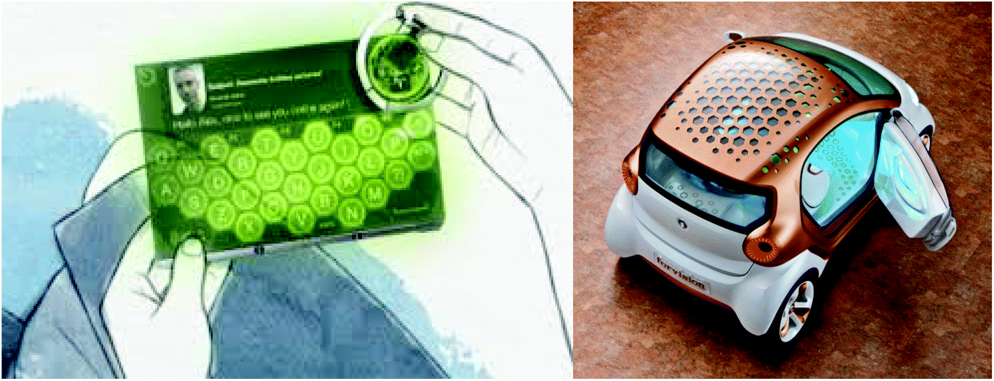 | ||
| Fig. 1 Morph1 (left) and SmartForVision2 (right) are examples of visionary applications where GRMs’ unique properties might be combined to enable new products. | ||
The STR is divided in 11 thematic chapters, summarized in Fig. 2. Each of them comprises a dedicated timeline. A final chapter presents two overall summary roadmaps.
 | ||
Fig. 2 Symbols associated with each theme. In the document, the symbol  is associated/replaced by the symbol is associated/replaced by the symbol  when we refer to industrial/large scale production. when we refer to industrial/large scale production. | ||
The present STR may not be fully complete, leaving out some of the most recent and rapidly evolving areas. We plan to present regular updates over the next 10 years to keep abreast with the latest developments in GRM science and technology. These include charge-based high speed electronic devices, as well as non-charge-based devices (e.g. spintronic devices) with novel functionalities. A key area is advanced methods to produce GRMs, combining structural functions with embedded electronics in an environmentally sustainable manner. The STR extends beyond mainstream ICT to incorporate novel sensor applications and composites that take advantage of the GRMs chemical, biological and mechanical properties. Beyond ICT, the STR reaches out to several related areas. Graphene's high electrical conductivity, σ, and large surface area per unit mass make it an interesting material for energy storage, e.g. in advanced batteries and supercapacitors. These could have a large impact on portable electronics and other key areas, such as electric cars. The prospect of rapidly chargeable lightweight batteries would give environmentally friendly transportation a push and advance the large scale implementation of electric cars as a key component in urban and suburban transport. Strong and lightweight composites would also allow us to build new cars, airplanes and other structures using less material and energy, and contribute directly to a more sustainable world, see Fig. 3.
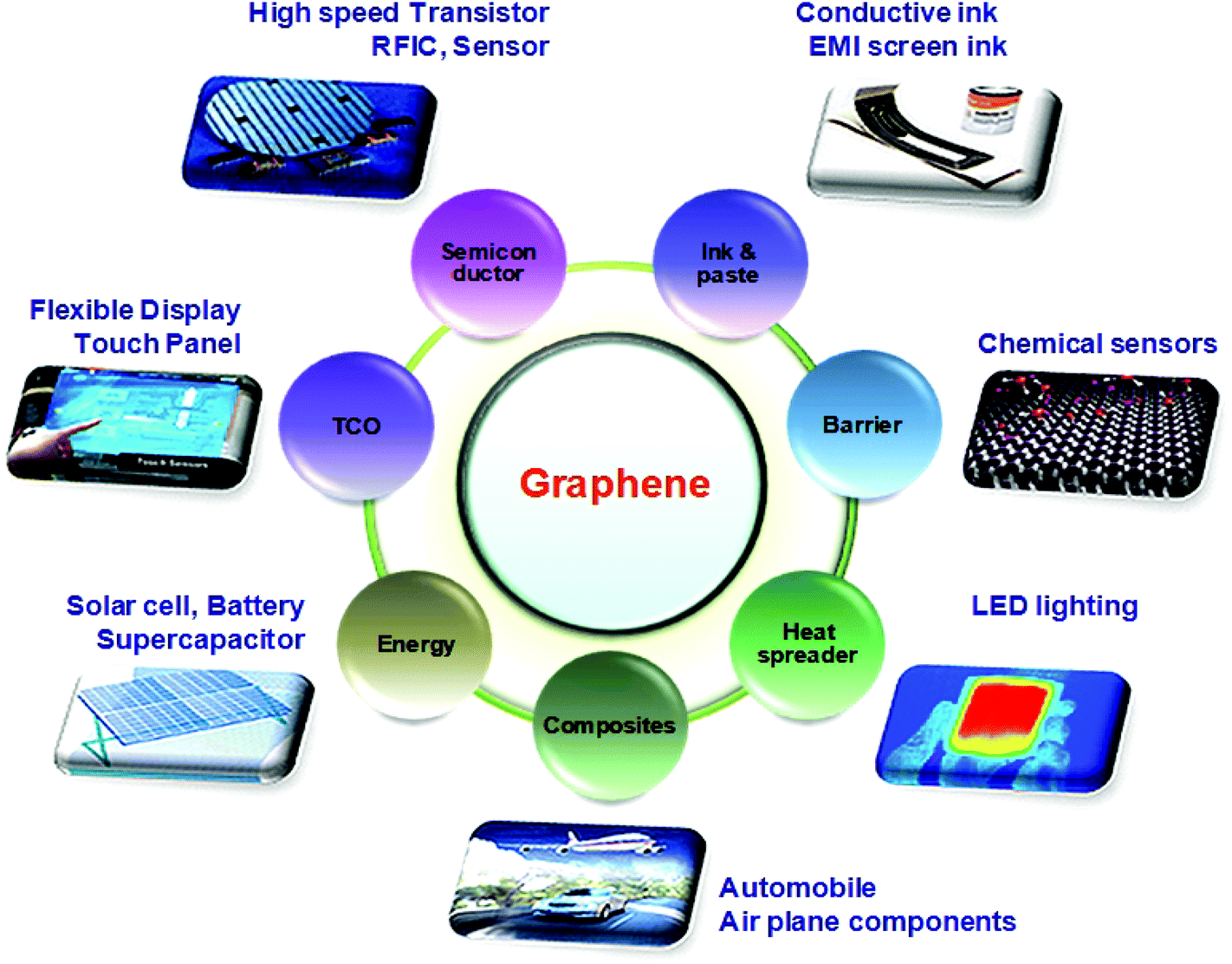 | ||
| Fig. 3 Overview of Applications of Graphene in different sectors ranging from conductive ink to chemical sensors, light emitting devices, composites, energy, touch panels and high frequency electronics. | ||
1.1. Graphene-based disruptive technologies: overview
Technologies, and our economy in general, usually advance either by incremental developments (e.g. scaling the size and number of transistors on a chip) or by quantum leaps (transition from vacuum tubes to semiconductor technologies). Disruptive technologies, behind such revolutions, are usually characterised by universal, versatile applications, which change many aspects of our lives simultaneously, penetrating every corner of our existence. In order to become disruptive, a new technology needs to offer not incremental, but orders of magnitude improvements. Moreover, the more universal the technology, the better chances it has for broad base success. This can be summarized by the “Lemma of New Technology”, proposed by Herbert Kroemer, who received the Nobel Prize in Physics in 2000 for basic work in ICT: “The principal applications of any sufficiently new and innovative technology always have been – and will continue to be – applications created by that technology”.3 Graphene is no exception to this lemma. Does graphene have a chance to become the next disruptive technology? Can graphene be the material of the 21st century?In terms of its properties, it certainly has potential. The 2010 Nobel Prize in Physics already acknowledged the profound novelty of the physical properties that can be observed in graphene: different physics applies, compared with other electronic materials, such as common semiconductors. Consequently, a plethora of outstanding properties have arisen from this material. Many are unique and superior to those of other materials. More importantly, such combination of properties cannot be found in any other material or material system. So, it is not a question of if, but a question of how many applications will graphene be used for, and how pervasive will it become. There are indeed many examples of “wonder” materials that have not yet lived up to expectations, nor delivered the promised revolution, while more “ordinary” ones are now pervasively used. Are the properties of graphene so unique to overshadow the unavoidable inconveniences of switching to a new technology, a process usually accompanied by large research and development (R&D) and capital investments? The advancing R&D activity on GRMs has already shown a significant development aimed at making GRMs suitable for industrial applications.
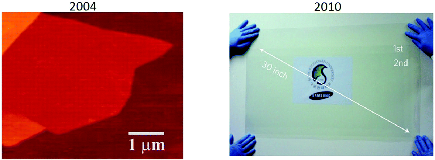
The production of graphene is one striking example of rapid development, with progress from random generation of micro-flakes in the laboratory5 to large-scale,6 roll-to-roll (R2R) processing of graphene sheets of sizes approaching the metre-scale7 (Fig. 4).
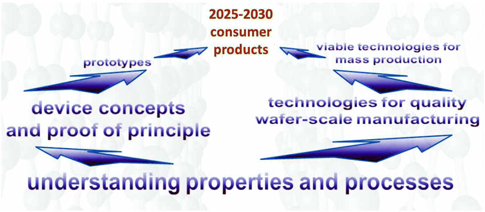
It is reasonable to expect a rapid clearing of further technological hurdles towards the development of a GRM-based industry in the coming years (Fig. 5).
 | ||
| Fig. 5 Towards GRM-based products. | ||
Therefore, in spite of the inherent novelty associated with GRMs and the lack of maturity of GRM technology, an initial roadmap can be envisaged, including short-term milestones, and some medium- to long-term targets, less detailed, but potentially more disruptive. This should guide the expected transition towards a technological platform underpinned by GRMs, with opportunities in many fields and benefits to society as a whole.
The upscaling of GRM production is steadily progressing, and challenges remain when it comes to maintaining the properties and performance upon up-scaling, which includes mass production for material/energy-oriented applications and wafer-scale integration for device/ICTs-oriented applications. Nevertheless, GRMs technology is expected to provide opportunities for the development of a novel platform, contributing to key technological fields with important social and economic impacts. The definition of “quality” of a GRM cannot be given in absolute terms, but strictly depends on the applications. E.g. the “quality” of graphene needed for high performance electronics is “the opposite” of that required for batteries or supercapacitors, in that the latter work better with materials having defects, voids and cavities, while the former require defect free, and flat material. This will be a challenge for standardization, since the materials properties will have to be defined in relation to a variety of possible applications.
1.1.1.1. New opportunities for electronics. The introduction of more functions in integrated electronic systems will enable applications in domotics (i.e. home automation by means of distributed sensors, actuators and controllers), environmental control, and office automation to meet the social request for better safety, health and comfort. An increase in automation should also consider the aging population and people at work, and the need of adequate facilities. Sensors or metrological devices based on GRMs can further extend functionalities of hybrid circuits. Three dimensional (3d) integration of GRMs-based devices may be conceivable in a Si flow, and could be the solution for low cost chips with extended functionalities.
Graphene has many record properties, see Fig. 6. It is transparent like (or better than) plastic, but conducts heat and electricity better than any metal, it is an elastic film, behaves as an impermeable membrane, and it is chemically inert and stable. Thus it seems ideal as the next generation transparent conductor. There is a real need to find a substitute for indium tin oxide (ITO) in the manufacturing of various types of displays and touch screens, due to the brittleness of indium that makes it difficult to use them when flexibility is a requirement.8 Graphene is an ideal candidate for such a task.9 Thus, coupled with carbon's abundance, this presents a more sustainable alternative to ITO. Prototypes of graphene-based displays have been produced7 and commercial products seem imminent.10
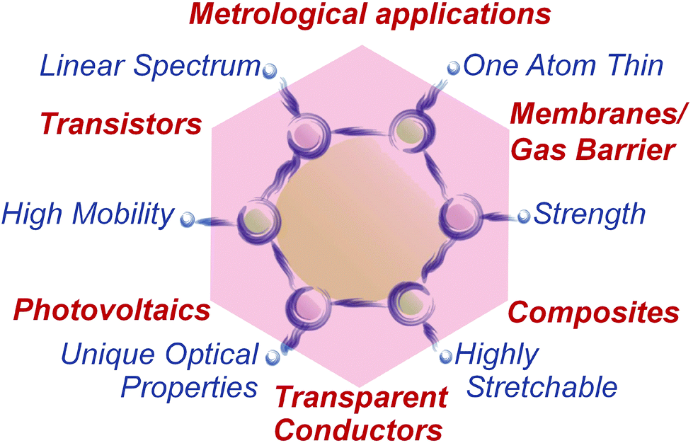 | ||
| Fig. 6 Graphene properties and application areas. | ||
In 2010, the first R2R production of 30-inch graphene transparent conductors (TC), with low sheet resistance (Rs) and 90% transmittance (Tr), competitive with commercial transparent electrodes, such as ITO, was reported.7 Graphene electrodes have been incorporated into fully functional touch-screens capable of withstanding high strain.10 Thus, one can envision the development of flexible, portable and reconfigurable electronics, such as the MORPH concept1 (Fig. 1 and 7).
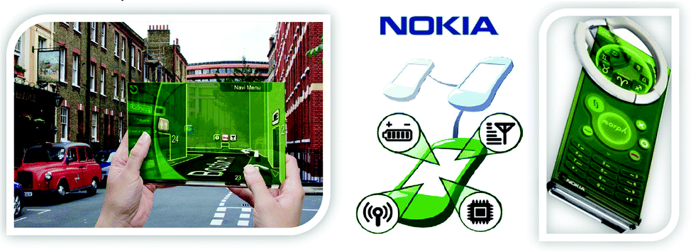 | ||
| Fig. 7 NOKIA Morph:1 the future mobile device will act as a gateway. It will connect users to local environment, as well as the global internet. It is an attentive device that shapes according to the context. It can change its form from rigid to flexible and stretchable.1 | ||
New horizons have opened with the demonstration of high-speed graphene circuits11 offering high-bandwidth, which might impact future low-cost smart phones and displays.
Complementary metal oxide semiconductor (CMOS) technology, as currently used in integrated circuits, is rapidly approaching the limits of downsizing transistors,12 and graphene is considered a possible candidate for post-Si electronics by the International Technology Roadmap for Semiconductors (ITRS).12 However, a graphene-based low power device meeting all of the requirements of CMOS technology has not been demonstrated yet. The technology needed to produce graphene circuits is still in its infancy, and growth of large area films with good electrical properties on flat dielectric surfaces has not yet been demonstrated. Novel architectures,13,14 not necessarily based on graphene ribbons,15 need to be developed.
In 2011 ref. 11 reported the first wafer-scale graphene circuit (broadband frequency mixer) in which all components, including graphene field-effect transistors (GFETs) and inductors, were integrated on a single SiC wafer. The circuit operated as a broadband Radio Frequency (RF) mixer at frequencies up to 10 GHz, with thermal stability and little reduction in performance (less than one decibel) in the temperature (T) range 300–400 K. This suggests that graphene devices with complex functionality and performance may be achieved.
Being just one atom thick, graphene appears as a suitable candidate to eventually realize a new generation of flexible electronic devices.14 Electronics on plastics or paper is low cost.16,17 It will offer the possibility to introduce more information on goods used on a daily basis, e.g. on food for safety and health, as well as on many other products. Bar codes may not be able to store all the required information. Magnetic strips or stand-alone memories do not offer the same opportunities as active electronics interacting in a wireless network. The possibility to develop passive components in GRMs (resistors, capacitors, antennas) as well as diodes (Schottky) or simple FETs, and the rapid growth of technology in this direction may enable RF flexible circuits in a wireless networked environment.
Thin and flexible GRMs-based electronic components might be obtained and modularly integrated, and thin portable devices might be assembled and distributed. Graphene can withstand mechanical deformation18 and can be folded without breaking.18 Such a feature provides a way to tune the electronic properties, through so-called “strain engineering”19 of the electronic band structure. Foldable devices can be imagined, together with a wealth of new device form factors, which could enable innovative concepts of integration and distribution.
By enabling flexible electronics, GRMs will allow the use of the existing knowledge base and infrastructures of various organizations working on organic electronics (organic LEDS as used in displays, conductive polymers, plastics, printable electronics), providing a synergistic framework for collecting and underpinning many distributed technical competences.
1.1.1.2. New energy solutions. GRMs could bring new solutions to the current challenges related to energy generation and storage, first in nano-enhanced products, then in new nano-enabled products. GRMs-based systems for energy production (photovoltaics, PV, fuel cells), energy storage (supercapacitors, batteries, and hydrogen storage) may be developed via relevant proof of concept demonstrators that will progress towards the targeted technology readiness levels (TRLs) required for industrial adoption. TRLs are used to assess the maturity of technologies during their development. The commonly used NASA scale,20,21 is shown in Fig. 8: 1. Basic principles observed and reported; 2. Technology concept and/or application formulated; 3. Analytical and experimental critical function and/or characteristic proof of concept; 4. Component and/or breadboard validation in laboratory environment; 5. Component and/or breadboard validation in relevant environment; 6. System/subsystem model or prototype demonstration in a relevant environment; 7. System prototype demonstration in an operational environment; 8. Actual system completed and qualified through test and demonstration. 9. Actual system proven through successful operations.
 | ||
| Fig. 8 TRL definitions, adapted from ref. 21. | ||
Furthermore, graphene technology may provide new power management solutions, key to allow efficient and safe use of energy. To date in Europe nearly the 60% of the energy is electrical (lighting, electronics, telecommunications, motor control).22 Of the remaining 40%, nearly all is used for transportation.22
1.1.1.3. New technologies and materials: towards a novel technological platform. GRMs may favour not only an improvement of existing technologies, such as electronics and optoelectronics, but may also enable the emergence of new technologies, currently hampered by intrinsic limitations. The GRMs' properties, with a qualitatively different physics with respect to the other commonly used materials, may enable technological concepts, thus far only theoretically possible, but not practically developed.
One example is that of spintronics,23 an emerging technology that exploits the spin rather than the charge of electrons as the degree of freedom for carrying information,24 with the primary advantage of consuming less power per computation.25 Although one spintronic effect – namely, giant magnetoresistance26 – is already a fundamental working principle in hard disk technology,27 the use of spintronic devices as a replacement for CMOS has not been realized yet. Scientific papers have highlighted graphene properties that are suitable for the development of spintronic devices,28–30 and many groups are now pursuing this.
Radically new technologies could be enabled by graphene, such as the so-called “valleytronics”,31 which exploits the peculiar “isospin”31 of charge carriers in graphene as a degree of freedom for carrying information. Further, there are some still not experimentally proven theoretical predictions, such as a “chiral superconductivity”,32 which may lead to completely new applications.
Taking just these few examples into account, we expect that the development of some new applications based on the salient properties of GRMs might happen in the coming years.
Graphene is also an ideal candidate for engineering new materials, and many examples have already been realised.33–36 The “all-surface” nature of graphene offers the opportunity to tailor its properties by surface treatments (e.g. by chemical functionalization33). E.g., graphene has been converted into a band-gap semiconductor (hydrogenated graphene, or “graphane”33) or into an insulator (fluorinated graphene, or “fluorographene”34). In addition, graphene flakes can be placed in dispersions.35 These retain many of its outstanding properties, and can be used for the realisation of composite materials (e.g. by embedding in a polymeric matrix36,37) with improved performance.35–37
Graphene is not only important for its own properties, but also because it is the paradigm for a new class of materials, which is likely to grow following the rise of graphene technology. Some examples have already been reported, such as hexagonal boron nitride (h-BN)5,38 and molybdenite monolayers5,38,39 The crystal structure of the latter was studied since 1923 by Dickinson and Pauling,40 with studies extended to a few layers in the sixties (a possible observation of monolayer MoS2 reported in the pioneering work of Frindt in Cambridge in 1963)41,42 and a definite identification of monolayer MoS2 in 1986.39 The assembly of such 2d crystals, i.e. by stacking different atomic planes (heterostructures43), or by varying the stacking order of homogeneous atomic planes,44 provides a rich toolset for new, customised materials. We expect that the lessons learnt developing graphene science and technology will drive the manufacturing of many other innovative materials.
At present, the realisation of an electronic device (such as, e.g., a mobile phone) requires the assembly of a variety of components obtained by many different technologies. GRMs, by including many properties, may offer the opportunity to build a comprehensive technological platform for different device components, including transistors, batteries, optoelectronic components, detectors, photovoltaic cells, photodetectors, ultrafast lasers, bio- and physicochemical sensors, etc. Such a change in the paradigm of device manufacturing may open big opportunities for the development of a new industry.
1.2. Scientific output
GRM research is an example of an emerging translational nanotechnology, where discoveries in laboratories are transferred to applications. This is evidenced, in part, by the rise in patenting activity since 2007 by corporations around the world.45 The concept of translational technology is typically associated with biomedicine,46 where it is a well-established link between basic research and clinical studies, but the principle can be applied more generally. A striking example is giant magnetoresistance,47 that moved from an academic discovery to a dominant information storage technology in a few years.48 Similarly, GRMs have the potential to make a profound impact: Integrating GRMs components with Si-based electronics, and gradually replacing Si in some applications, allows not only substantial performance improvements but, more importantly, new applications.Carbon has been the driving force behind several technological revolutions: in the 19th century, energy production by burning carbon was integral to the industrial revolution;49 in the 20th century, carbon-based plastics revolutionized the manufacturing industry;50 in the 21st century, graphitic carbon might be a key component in a third technological revolution.
The growth of publications on GRMs is shown in Fig. 9, with no sign of slowing down. The reasons for the growth of research on GRMs are manifold. First, graphene is a material with a unique set properties. Either separately or in combinations, these can be exploited in many areas of research and applications; new possibilities are being recognized all the time as the science of GRMs progresses. Second, graphene Science and Technology (ST) relies on one of the most abundant materials on earth,51 carbon. It is an inherently sustainable and economical technology. Thirdly, graphene is a planar material and, as such, compatible with the established production technologies in ICT, and integrable with conventional materials such as Si. Combined, these premises give realistic promise of creating a new, more powerful and versatile, sustainable and economically viable technology platform. As a result, graphene research has already emerged as the top research front in materials science.52 However, due to the unique structure of graphene, many of the possibilities it offers are still poorly understood, and their analysis requires highly sophisticated methods; To quote the Nobel Laureate Frank Wilczek: «graphene is probably the only system where ideas from quantum field theory can lead to patentable innovations».46
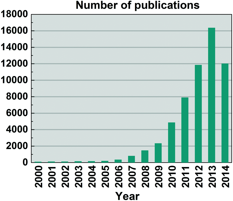 | ||
| Fig. 9 Publications on graphene from 2000 to Aug. 2014 (thus, well over 18000 are expected by end 2014). Source ISI Web of Science (search: Topic = Graphene). Publications on graphene prior to 2000 are not plotted. | ||
Overall, the graphene patent landscape is growing rapidly and already resembles that of sub-segments of the semiconductor and biotechnology industries,56 which experience high levels of patent activity. The patent strategies of the businesses active in such sub-sectors frequently include ‘portfolio maximization’56 and ‘portfolio optimization’56 strategies, and the sub-sectors experience the development of what commentators term ‘patent thickets’56, or multiple overlapping granted patent rights.56 A range of policies, regulatory and business strategies have been developed to limit such patent practices.57 In such circumstances, accurate patent landscaping may provide critical information to policy-makers, investors and individual industry participants, underpinning the development of sound policies, business strategies and research commercialisation plans.
The analysis of the top graphene patent owners (patent assignees) and their patent applications, illustrates the broad relevance of graphene to diverse industry sectors, such as automotive, computing and industrial chemicals.58 The uses of patents between and within these industry sectors and over time can vary widely, adding to the navigational challenges that face readers of even the most accurate graphene IP maps.
Understanding and correctly navigating the rapidly growing patent landscape will be crucial to those who seek to secure future value from GRM research. Patents may be particularly important to the realisation of future commercial value, as patents are a form of IP important to the business models and business practices observed in many of the technology sectors in which GRM research is and will be deployed.56
The IP analysis and discussion in section 1.2.2 highlights the disparity between graphene-related scientific production (represented by publications), see Fig. 9, 10, and graphene-related patent applications (associated with technical exploitation), providing additional evidence of the need for a large scale, concentrated action to bring together leading players in academia (who are, broadly, responsible for scientific production) and industrial leaders (who are, broadly, responsible for patent applications).
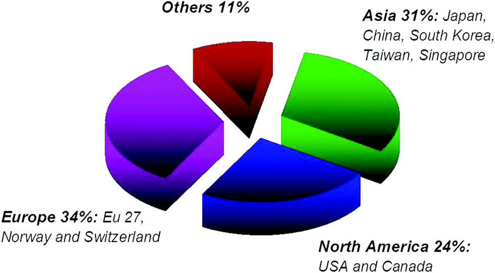 | ||
| Fig. 10 Geographical distribution of scientific papers on graphene as of December 2013. | ||
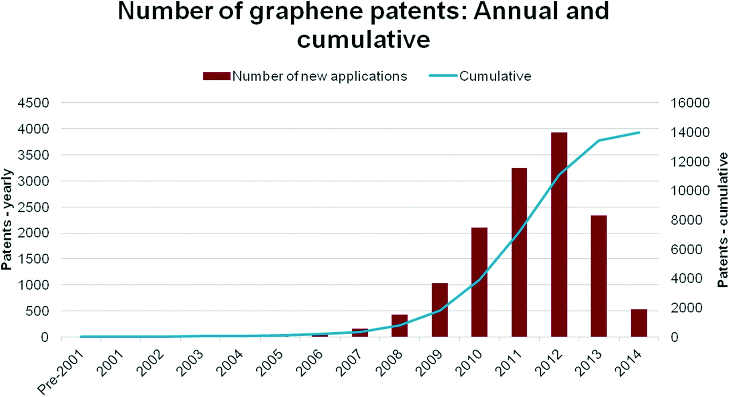 | ||
| Fig. 11 Patent applications on graphene as a function of application year. Note: patents remain unpublished for up to 18 months from their filing. Accordingly, 2013 and 2014 are under-represented. Data updated as of July 2014. | ||
The patent space prior to 2006 is dominated by US research institutions and start ups, with a significant volume of filings starting after 2006. The surge in filings from 2007 has been driven heavily by innovations from South Korean multinationals, especially Samsung, as well as research institutes with Samsung connections.
A detailed review of the patent dataset reveals that patents have been filed for a very diverse range of applications including characterization,60 polymer composites,61 transparent displays,62 transistors,63 capacitors,64 solar cells,65 biosensors,66 conductive inks,67–69 windows,70 saturable absorbers,71 photodetectors,72 tennis rackets.73 However, overall, the graphene patent space comprises patent filings in two main sectors: synthesis (e.g. production of graphene by chemical vapour deposition – CVD, exfoliation, etc.,) and electronics (e.g. use of graphene for displays, transistors and computer chips), each ∼30% of the total space, as for Fig. 12, although there is some overlap between sectors. Such overlapping filings can be the result of cross-disciplinary research and can provide evidence of ‘transformational’ and ‘disruptive’ technologies.
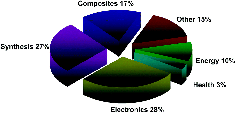 | ||
| Fig. 12 Proportion of overall graphene patents, by sector as of July 2014. | ||
Considering the wide range of potential graphene applications, indicative of crossing vertical technology ‘silos’ (with applications in sectors as diverse as electronics, ICT, energy, consumer goods, polymers, automotive industry, medicine, and industrial chemicals/catalysis), the dominance of synthesis and electronics alone suggests this is an early stage space with plenty of scope for development.
Additionally, given the relatively young age of this space and the demands for mass-production, the strong drive toward synthesis observed in the patent data is unsurprising.74 As the underlying graphene technology space develops and the patent space matures, re-distribution seems inevitable, probably away from synthesis and towards the currently less well-established (or not yet conceived) end-use applications.
Our analysis of filing geography gives an indication of the key innovation locations and potential markets. This interpretation is further supported by noticing that the patenting trend closely follows the standard technology evolution pattern as discussed in ref. 75.
Fig. 13 plots the geographical breakdown of graphene patent filings by filing jurisdiction. Companies tend to file first in their home jurisdiction. The second filing location (other than in the case of an international Patent Cooperation Treaty – PCT – application) is likely to be a key market or a key manufacturing location.
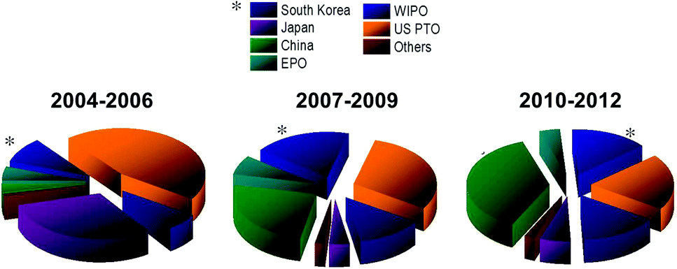 | ||
| Fig. 13 Graphene patent filing authorities. EPO, European patents office; WIPO, World Intellectual Property Organization; US PTO United States Patent and Trademark Office. | ||
Fig. 13 provides evidence of a relative increase in graphene patent filings in South Korea from 2007 to 2009 compared to 2004–2006. This could indicate increased commercial interest in graphene technology from around 2007. The period 2010 to 2012 shows a marked relative increase in graphene patent filings in China. It should be noted that a general increase in Chinese patent filings across many ST domains in this period is observed.76 Notwithstanding this general increase in Chinese patent activity, there does appear to be increased commercial interest in graphene in China. It is notable that the European Patent Office contribution as a percentage of all graphene patent filings globally falls from a 8% in the period 2007 to 2009 to 4% in the period 2010 to 2012.
The importance of the US, China and South Korea is emphasised by the top assignees, shown in Fig. 14. The corporation with most graphene patent applications is the Korean multinational Samsung, with over three times as many filings as its nearest rival. It has also patented an unrivalled range of graphene-technology applications, including synthesis procedures,77 transparent display devices,78 composite materials,79 transistors,80 batteries and solar cells.81 Samsung's patent applications indicate a sustained and heavy investment in graphene R&D, as well as collaboration (co-assignment of patents) with a wide range of academic institutions.82,83
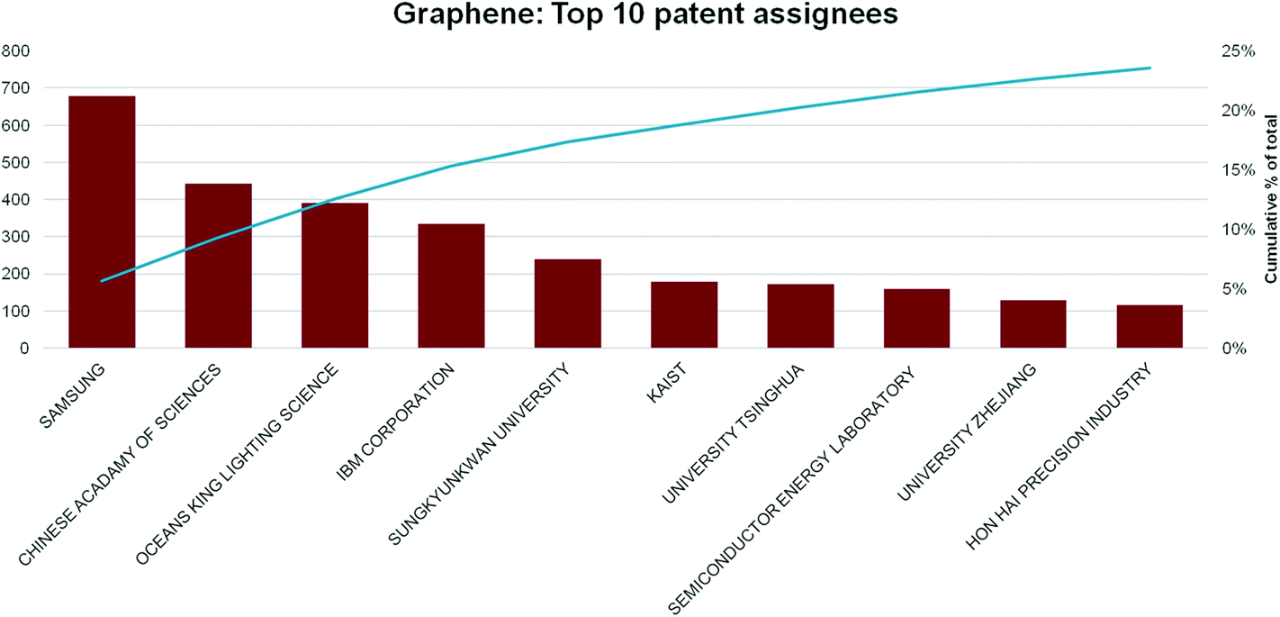 | ||
| Fig. 14 Top 10 graphene patent assignees by number and cumulative over all time as of end-July 2014. Number of patents are indicated in the red histograms referred to the left Y axis, while the cumulative percentage is the blue line, referred to the right Y axis. | ||
It is also interesting to note that patent filings by universities and research institutions make up a significant proportion (∼50%) of total patent filings: the other half comprises contributions from small and medium-sized enterprises (SMEs) and multinationals.
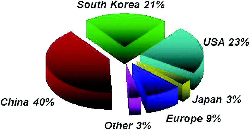
Europe's position is shown in Fig. 10, 12 and 14. While Europe makes a good showing in the geographical distribution of publications, it lags behind in patent applications, with only 7% of patent filings as compared to 30% in the US, 25% in China, and 13% in South Korea (Fig. 13) and only 9% of filings by academic institutions assigned in Europe (Fig. 15).
 | ||
| Fig. 15 Geographical breakdown of academic patent holders as of July 2014. | ||
While Europe is trailing other regions in terms of number of patent filings, it nevertheless has a significant foothold in the patent landscape. Currently, the top European patent holder is Finland's Nokia, primarily around incorporation of graphene into electrical devices, including resonators and electrodes.72,84,85
European Universities also show promise in the graphene patent landscape. We also find evidence of corporate-academic collaborations in Europe, including e.g. co-assignments filed with European research institutions and Germany's AMO GmbH,86 and chemical giant BASF.87,88 Finally, Europe sees significant patent filings from a number of international corporate and university players including Samsung,77 Vorbeck Materials,89 Princeton University,90–92 and Rice University,93–95 perhaps reflecting the quality of the European ST base around graphene, and its importance as a market for graphene technologies.
There are a number of features in the graphene patent landscape which may lead to a risk of patent thickets96 or ‘multiple overlapping granted patents’ existing around aspects of graphene technology systems. There is a relatively high volume of patent activity around graphene, which is an early stage technology space, with applications in patent intensive industry sectors. Often patents claim carbon nano structures other than graphene in graphene patent landscapes, illustrating difficulties around defining ‘graphene’ and mapping the graphene patent landscape. Additionally, the graphene patent nomenclature is not entirely settled. Different patent examiners might grant patents over the same components which the different experts and industry players call by different names. Use of a variety of names for the same components could be a deliberate attempt at obfuscation. There is some support for this view in the relevant academic literature. E.g., ref. 97 suggested that where patent assessment quality is low (e.g. due to inadequate expertise by patent examiners of a particular technology space), leading players might engage in high-volume patenting to deliberately create a ‘patent thicket’, with a range of possible negative effects on innovation.98
Despite the challenges described above, there are a number of important opportunities of which academics, SMEs and multinationals should take advantage, including increased occurrences of academia-industry collaboration (following the lead of South Korea and the US); preparing for the inevitable re-distribution of the graphene patent space as it matures and, most likely, moves away from synthesis, towards the currently less well-established (or not yet conceived) end-use applications.
2. Fundamental research
One of the reasons for the fast progress of graphene research is the wealth of its unique properties. However, what makes it really special, and gives it a disruptive value, is that all those properties are combined in a single material. Transparency–conductivity–elasticity can find use in flexible electronics, high mobility (μ)-ultimate thinness in efficient transistors for RF applications, while transparency–impermeability–conductivity can be exploited for transparent protective coatings. The list of such combinations is ever growing. The most important are probably those not yet explored, as they might lead to new applications.Currently, several record high characteristics have been achieved with graphene, some of them reaching theoretically predicted limits: room temperature (RT) μ of 2.5 × 105 cm2 V−1 s−1 (ref. 99) and μ ∼ 6 × 106 cm2 V−1 s−1 at 4 K,100 a Young modulus of 1 TPa and intrinsic strength of 130 GPa;18 impermeability for gases101 and so on. Graphene also has record high thermal conductivity κ (∼2000 to 5300 W m−1 K−1 (ref. 102) and can withstand high current densities (million times higher than copper).103
The surge in graphene research also paved the way for experiments on many other 2d crystals.5 One can use similar strategies to graphene to get new materials by mechanical5 and liquid phase exfoliation of LMs38 or CVD. An alternative strategy to create new 2d crystals is to start with existing ones (e.g. graphene) and use them as atomic scaffolding for modification by chemical means (graphane33 or fluorographene34). The resulting pool of 2d crystals is huge, and covers a range of properties: from the most insulating to the best conductors, from the strongest to the softest. Suitable properties may be used depending on the targeted application. E.g., to cover a range of various conductance properties (but keeping the strength) one might use combinations of graphene and fluorographene, the latter being insulating, but almost as strong as the former.
For the long-term future, opportunities can be envisioned, combining conducting graphene with semiconducting and optically active 2d crystals, to create hybrid multilayer superstructures. If 2d crystals hold a wide variety of properties, the sandwiched structures of 2, 3, 4… layers of such materials can further offer longer term prospectives. By assembling 2d structures, one can engineer artificial 3d crystals, displaying tailored properties. Since such 2d based heterostructures104,105 can be assembled with atomic precision and individual layers of very different identity can be combined together, the properties could in principle be tuned to fit any application. Furthermore, the functionality of those stacks is embedded in the design of such heterostructures. First proof of principle devices are already available,106 such as vertical tunnelling transistors106 which show promising electrical characteristics.107,108 Starting with fundamental studies, the aim is to learn how to tune properties of such hetero- or hybrid systems in order to target a specific functionality.
Exploiting the full potential offered by the electronic and mechanical properties of GRMs in applications requires extensive fundamental studies. Graphene transistors and interconnects have an opportunity to complement and extend current Si technology. One route towards the use of graphene transistors for logic devices relies on creating a controllable band gap. The limited on/off current ratio (ION/IOFF) may be resolved in new transistor designs, which exploit the modulation of the work function of graphene,109 or carrier injection from graphene into a fully-gapped semiconductor,110 by gaining control over vertical (rather than planar) transport through various barriers,106 or using graphene as a gate, electrode, or interconnect. For the latter application of graphene, its electrical and thermal conductivities play an important role, so that studies of those properties should be intensified, especially in polycrystalline CVD-material.
Nature offers a very broad class of 2d crystals. There are several LMs which retain their stability in the form of monolayer and whose properties are complementary to those of graphene. Transition metal oxides (TMOs) and transition metal dichalcogenides (TMDs) also have a layered structure.111 Atoms within each layer are held together by covalent bonds, while van der Waals (vdW) interactions hold the layers together.111 LMs include a large number of systems with interesting properties.111E.g., NiTe2 and VSe2 are semi-metals,111 WS2, WSe2, MoS2, MoSe2, MoTe2, TaS2, RhTe2, PdTe2 are semiconductors,111 h-BN, and HfS2 are insulators, NbS2, NbSe2, NbTe2, and TaSe2 are superconductors.111 Moreover, there are other LMs such as Bi2Se3, Bi2Te3 that show thermoelectric properties111 and may behave as topological insulators (TIs).112 Atomic layers of these materials can be produced,5 using mechanical or liquid-phase exfoliation, see section 4 for more details on production.
A wider variety of 2d materials are also being explored, such as the graphene analogue of silicon (i.e., silicene),113,114 germanium (i.e., germanene),115 phosphorus (i.e., phosphorene)116 and tin (i.e., stanene).117,118 Another large LM class is that comprising the MXenes.119,120 These are derived by exfoliating the so called MAX Phases, i.e. layered, hexagonal carbides and nitrides having the general formula: Mn+1AXn, (MAX) where n = 1 to 3, M is an early transition metal, A is an A-group (mostly IIIA and IVA, or groups 13 and 14) element and X is either carbon and/or nitrogen.
Chemical modification of graphene33 allows the creation of another class of 2d crystals with a non-zero bandgap, such as graphane33 and fluorographene.34 Modification of these materials is interesting, e.g. p-doped graphane could be an electron–phonon superconductor121 with a critical temperature (Tc) above 77 K.121
There is also a growing number of graphane analogues, such as germanane,122 and stanane.123Ref. 122 synthesized mm-scale crystals of hydrogen-terminated germanane from the topochemical deintercalation (i.e., selective for a specific chemical element) of CaGe2 resulting in a lattice of Ge atoms with an analogous geometry to the sp3-hybridized graphane surface, in which every Ge atom is terminated with either H or OH above or below the layer.124 Germanane is thermally stable up to 75 °C.122 Above this T, dehydrogenation and amorphization begin to occur.122
2.1. Electronic transport
Graphene's promise to complement or even replace semiconductors in micro- and nanoelectronics is determined by several factors. These include its 2d nature, enabling easy processing and direct control of the charge carriers, fast moving (quasi-relativistic) electronic excitations yielding a high μ (almost equal between electrons and holes) – both at RT and low T, and high κ. Graphene crystals have two well-established allotropes, single layer graphene (SLG), where charge carriers resemble relativistic Dirac particles,125 and bilayer graphene (BLG), where electrons also have some Dirac-like properties, but have a parabolic dispersion.125 However, unlike SLG, where the absence of a gap is protected by the high symmetry of the honeycomb lattice, BLG is more versatile: a transverse electric field can open a gap126–128 and its low-energy band structure can be qualitatively changed by strain.129 Each of these has advantages and disadvantages for a given application, and one has to learn how to control and exploit them to create functional devices.Concerning μ, further research is needed to understand the effects of defects and charge inhomogeneities, as well as development of doping techniques. The influence of various dielectric substrates or overgrown insulators also needs further basic understanding in order to optimize device performance. Further studies of transport regimes and optoelectronic effects in gapped BLG are needed for FET applications. Considering the possible use of an electrically induced gap in BLGs for quantum dots (QDs) and engineered QDs-based circuits (e.g., for quantum information processing130), a detailed understanding of the influence of disorder and Coulomb interaction on the T dependence of conductivity is required, including the nature of variable range hopping in gapped BLGs, which can be generically described by an exponential increase of resistance following R ∼ exp[(T0/T)p] (ref. 131) with T0 a constant depending on the localization length and density of states, whereas the exponent is given by p = 1/2 for the Efros–Shklovskii mechanism132 and p = 1/3 for the Mott hopping regime;131 the dominating regime depending on the material.133
Besides the studies of sample-average graphene parameters, such as, Rs, it is highly desirable to get insights into local properties of graphene used in devices. This can be achieved by means of several non-destructive techniques: Raman spectroscopy,134–136 Kelvin probe microscopy,137 local compressibility measurements,138 and non-contact conductivity, using capacitive coupling of a probe operated at high frequency.139 The application of such techniques to graphene is natural, due to its 2d nature. These techniques can be used to study GRMs to reveal the role of inhomogeneity in carrier density, the role of particular substrates, and can shed light on the role of structural defects and adsorbents in limiting device performance.
The peculiar properties of electrons in SLG (their similarity to relativistic Dirac particles) make a p–n junction in graphene transparent to electrons arriving at normal incidence.140,141 On one hand, this effect, known as Klein tunneling,141 makes it difficult to achieve a complete pinch-off of electric current, without chemical modification or patterning.142 On the other hand, it offers a unique possibility to create ballistic devices and circuits where electrons experience focusing by one or several p–n interfaces.143 The development of such devices requires techniques of non-invasive gating [see, e.g., ref. 144]. Another method to improve quality of graphene is to suspend it over electrodes (also used as support) and then clean it by current annealing.144,145 This enables one to achieve highly homogeneous carrier density, and micron-long mean free paths, enabling a detailed investigation of electronic properties at very low excitation energies.145
Understanding the transport properties of graphene also includes its behaviour in the presence of a strong – quantising – magnetic field. As a truly 2d electron system, graphene displays the fundamental phenomenon of quantum Hall effect (QHE),146–150 which consists in the precise quantisation of Hall resistance of the device.150 Both integer and several fractional QHE (FQHE) states have been observed,151,146,148 the latter requiring very high crystalline quality and pure material,151 where the Coulomb interactions between electrons can become very strong, leading to the formation of correlated states of matter.152 The QHE robustness in SLG opens a possibility to explore one, up to now, impossible regime of quantum transport in solid-state materials: the interplay between QHE and superconductivity in one hybrid device made of graphene and a superconductor with a high critical magnetic field (e.g., a NbTi alloy153). Moreover, the particular robustness of QHE in graphene on the Si face of SiC154 (still waiting for a complete understanding155) makes it a suitable platform for a new type of resistance standard.154
One of the issues in the fabrication of GFETs is electrostatic gating. Atomic Layer Deposition (ALD) of high- [where is the dielectric constant] dielectrics (Al2O3, HfO2) is one possibility worth further exploration, due its accurate control of layer thickness.156 After such processing, graphene can be transferred to a Si substrate in which deep trenches previously filled with metal (e.g., W) form the back-gate, and the source and drain are subsequently deposited on the graphene itself. Such an approach offers a possibility to build devices with complex architectures. However, ALD uses alternating pulses of water and precursor materials157 and, since graphene is hydrophobic,158 the deposition of a uniform, defect-free dielectric layer is difficult,159 and requires further optimization. Another promising technological advance is offered by photochemical gating.160 There are several polymers where UV light converts Cl atoms into acceptors, whereas thermal annealing returns them into a covalently bound state.161 Due to easy charge transfer between graphene and environment, UV illumination can modulate carrier density in graphene covered by such polymers, enabling non-volatile memory cells.162
For device applications, graphene contacts with metals and semiconductors require further studies: charge transfer between materials, formation of Schottky barriers, and graphene p–n junctions. The contacts play a crucial role for several devices: for superconducting proximity effect transistors,163 where they determine how Cooper pairs penetrate graphene, and for transistors used to develop quantum resistance standard, also needing very low resistance contacts to reduce overheating at the high-current performance of the resistance standard. Chosen to match the work functions of graphite and metals, the most common combinations are Cr/Au,164 Ti/Au164,165, Ti/Pt,166 and Ti/Pd/Au,167 the latter exhibiting lower contact resistances in the 10−6 Ω cm−2 range.167 The best results to date, down to 10−7 Ω cm−2, were obtained for Au/Ti metallization with a 90 s O2 plasma cleaning prior to the metallization, and a post-annealing at ∼460 °C for 15 min.168
2.2. Spectroscopic characterization
Spectroscopy is an extremely powerful non-invasive tool in graphene studies. Optical visibility of graphene, enhanced by an appropriately chosen substrate structure,169–171 makes it possible to find flakes by inspection in an optical microscope. While a trained person can distinguish SLG from FLG by “naked eye” with high fidelity, Raman spectroscopy has become the method of choice for a more systematic analysis.134–136The Raman spectrum of graphite was measured 44 years ago.172 Since then, Raman spectroscopy has become a commonly used characterisation technique in carbon ST, as a method of choice to probe disordered and amorphous carbons, fullerenes, nanotubes, diamonds, carbon chains, and poly-conjugated molecules.173 The Raman spectrum of graphene was first reported in 2006.134 This triggered a huge effort to understand phonons,134,136 electron–phonon,134,136,174 magneto-phonon,175–177 and electron–electron178 interactions, and the influence on the Raman process of number134 and orientation134,136 of layers, electric179–181 or magnetic182,183 fields, strain,129,184 doping,179,185 disorder,136 defects,186 quality187 and types187 of edges, functional groups.188 The graphene electronic structure is captured in its Raman spectrum that evolves with the number of graphene layers (N).134 The 2D peak changes in shape, width, and position for increasing N (see Fig. 16), reflecting the change in the electron bands. The 2D peak is a single band in SLG, whereas it splits in four in BLG.134 Since the 2D shape reflects the electronic structure, twisted multi-layers can have 2D peaks resembling SLG.134 FLGs can also be characterized by the interlayer shear mode189 (see Fig. 17), i.e. the C peak that probes the interlayer coupling.190 This peak scales from ∼44 cm−1 in bulk graphite to ∼31 cm−1 in BLG (see Fig. 17).190 Layer breathing modes (LBMs) can also be observed in the Raman spectra of FLGs, via their resonant overtones in the range 80–300 cm−1.191 They can also be addresses through the stokes and anti-stokes combinations with the D' peak,134,196 or in twisted samples.2335
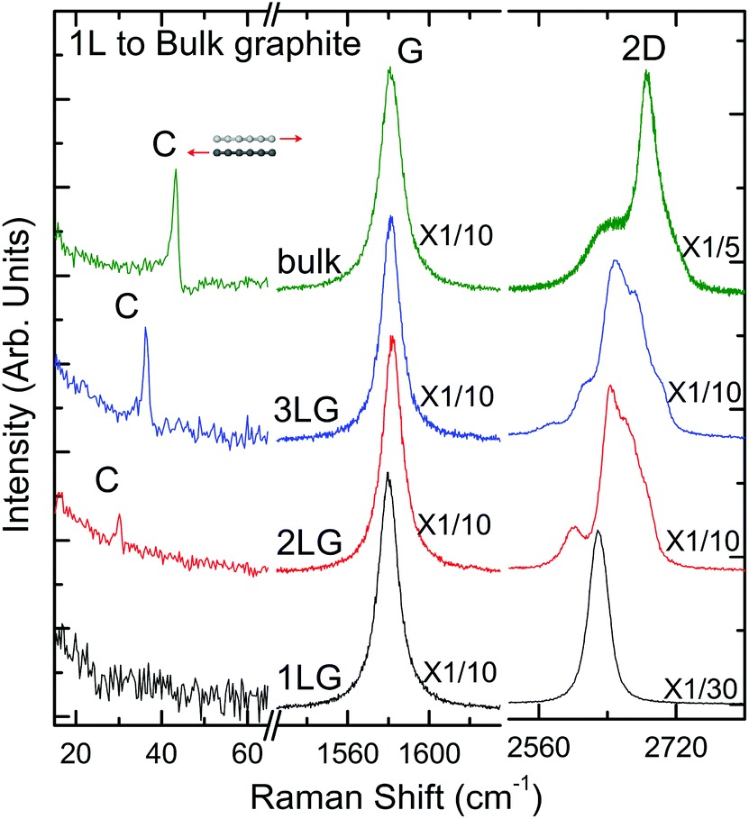 | ||
| Fig. 16 Raman spectra of SLG (1LG), BLG (2LG), TLG (3LG), and bulk graphite measured at 633 nm. Adapted from ref. 204. | ||
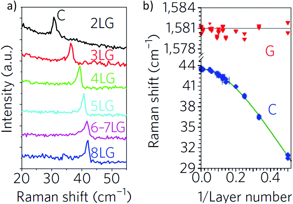 | ||
| Fig. 17 (a) C peak as a function of number of layers. (b) Fitted C- and G-peak position as a function of inverse number of layers. Adapted from ref. 134. | ||
It is important to note that, although being an in-plane mode, the 2D peak is sensitive to N because the resonant Raman mechanism that gives rise to it is closely linked to the details of the electronic band structure,135,136 the latter changing with N, and the layers relative orientation.192 On the other hand, the C peak and LBMs are a direct probe of N,190,191,193–196 as the vibrations themselves are out of plane, thus directly sensitive to N. Raman spectroscopy has provided key insights in the related properties of all sp2 carbon allotropes, graphene being their fundamental building block, and other carbon-based materials, such as amorphous, nanostructured and diamond-like carbons173,188,197–203 Raman spectroscopy has also huge potential for LMs,204,205 other than graphene, see section 2.8.1.
Studies of the magneto-phonon resonances206,207 enable to directly measure the electron–phonon coupling in SLG, BLG, and multilayers.177,206–208,209–211 Optical spectroscopy allows to study the split-bands in BLG,212,213 and the analysis of disorder-induced phonon-related Raman peaks134 provides information on sample quality complementary to that extracted from transport measurements.
Angle-resolved photoemission spectroscopy (ARPES) directly probes band dispersions and lattice composition of electron states, which determine the pseudospin symmetry of electronic states.214,215
Further improvement of the above-mentioned optical characterisation techniques and development of new approaches are critically important for in situ monitoring. Outside the visible-range and Infra-Red (IR) optical spectroscopy, detailed studies of defects in graphene can be addressed using scanning transmission electron microscopy (STEM), energy loss spectroscopy, low-angle X-ray spectroscopy, and resonant inelastic X-ray scattering (RIXS). The development of a standardised optical characterisation toolkit with the capability to monitor N, as well as quality and doping level, is one of the key needs for the progress in graphene mass manufacturing. Since there are several routes towards viable mass production, described in section 4, the suitable energy/wavelength range for the standardised spectroscopic characterisation toolkit is not known yet, thus spectroscopic studies of graphene need to be carried out over a broad energy range, from microwaves and far IR to UV and X-ray.
Scanning tunnelling microscopy (STM) is another important tool. Since electronic states in graphene can be directly addressed by a metallic tip,216 STM studies may be instrumental for understanding the morphology and electronic structure of defects: vacancies, grain boundaries (GBs), functionalised faults, and strongly deformed regions (‘bubbles’) resulting from processing or transfer. Such studies will be necessary for materials manufactured using each of the methods discussed in section 4, and to investigate the result of subjecting graphene to various gases. The use of STM under extreme conditions, such as strong magnetic fields, can probe local properties of electrons in Landau levels, and their structure close to defects.
2.3. Magnetism and spin transport
The control and manipulation of spins in graphene may lead to a number of novel applications and to the design of new devices, such as spin-based memories217 or spin logic chips.218 Graphene is uniquely suitable for such applications, since it does not show sizeable spin–orbit coupling,74 and is almost free of nuclear magnetic moments.219 Graphene currently holds the record for the longest spin relaxation length at RT, initially evaluated to be ∼5 μm,219 with promise for applications.220–222 At lower T, there are indications that the spin relaxation length could approach ∼100 μm.223 Further studies require the investigation of spin injection, diffusion, relaxation and of the interfaces between graphene and magnetic materials.The magnetic properties of graphene are connected to the defects. As a 2d electronic system, graphene is intrinsically diamagnetic.224 However, defects in graphene, as well as localisation of electrons in or around defects (vacancies, edges and covalently bonded dopants) can generate localised magnetic moments which directly modulate the spin current, as it has been proven in the cases of hydrogen adatoms and lattice vacancies.225,226
Edge magnetism has been predicted in graphene nanoribbons (GNRs) for certain edge geometries;227 the structure of graphene nanomesh, obtained by using block-copolymer nanopatterning of graphene, was also theoretically shown to yield RT magnetic states affecting spin transport.228
An enhanced paramagnetic signal was measured in graphene crystallites,229 and it was found that magnetism is enhanced in irradiated samples,229 similar to graphite.230 Strong enhancement of paramagnetism was also observed in fluorographene.231
An unambiguous assessment of the nature and the formation of magnetic moments in graphene and in FLG, and the resulting control of their properties would be a major advance and would significantly expand graphene applications.
The necessary steps towards a full portrait of graphene's magnetic properties are a complete understanding of disorder as well as (quantum) confinement (as for graphene quantum dots, GQDs, and GNRs) on spin relaxation and dephasing. This requires the investigation of the limits of conventional spin relaxation mechanisms common to metals and small gap semiconductors, i.e. Elliot–Yafet (EY)232,233 and Dyakonov–Perel234 (DP). EY was originally232,233 derived for spin relaxation in metals, and relates the spin dynamics with electron scattering off impurities or phonons.232,233 Each scattering event changes the momentum, with a finite spin-flip probability, that can be derived by perturbation theory (assuming weak spin–orbit scattering). This gives rise to a typical scaling behaviour of the spin relaxation time proportional to the momentum scattering time. DP234 is an efficient mechanism of spin relaxation due to spin orbit coupling in systems lacking inversion symmetry.234 Electron spins precess along a magnetic field which depends on the momentum.234 At each scattering event, the direction and frequency of the precession change randomly. The scaling behaviour is opposite to EY, with a spin relaxation time which is inversely proportional to the momentum scattering time.235
Two other mechanisms of spin relaxation in graphene have been proposed.236,237 One involves local magnetic moments which produce resonances and fast spin relaxation based on the resonant scattering of electrons off magnetic moments, which can be due to nonmagnetic adatoms, organic molecules, or vacancies.236 The other is related to the interplay between spin and pseudospin quantum degrees of freedom when disorder does not mix valleys.237 Such strong contribution of spin/pseudospin entanglement is particularly important when defects or impurities at the origin of local Rashba spin–orbit coupling (i.e. a momentum-dependent splitting of spin bands in 2d systems)238 preserve the pseudospin symmetry and lead to very long mean free path.
The role of edges on spin scattering and relaxation has yet to be clarified, as well as the case when the injected spin-polarized charges flow in close proximity (and interact) with other extrinsic spins (in localized or more extended charged states, located below or on top of the graphene).
The role of the substrate, contacts and environmental conditions on spin relaxation needs to be clarified. A detailed comparison between exfoliated graphene on SiO2, graphene on BN, and graphene grown on SiC is still missing. This would allow the classification of materials and devices' parameters, which have, to date, shown limited spin transport. These results could be compared with spin transport and relaxation in suspended graphene devices, which would provide the reference clean system. This is of fundamental importance for further exploration of more complex uses of the spin degree of freedom inside technology.
A systematic comparison of spintronic systems based on SLG, BLG and FLG still needs to be carried out. With a focus on spin ensembles, the RT capability of graphene devices has to be ascertained.
The knowledge derived from these investigations could be exploited in multiple ways. E.g., novel studies could be carried out to induce (para-) magnetism by introducing localised defect states in a controlled way, or by decoration of the surface with magnetic atoms or molecules. In the search for fingerprints of local magnetic ordering states and magnetoresistance profiles, chemically modified graphene (CMG)-based materials should be produced to investigate the potential of new physical phenomena. Other topics include studying electronic transport in graphene in proximity of ferromagnetic materials or ferromagnetic insulators (magnetic oxides as EuO, EuS, high-Curie T (above which the magnetic state of the system is lost) Yttrium Iron Garnet (YIG), NiO, CoFe2O4). This may induce spin polarization, which could be exploited to demonstrate spin filtering effects.239 Related issues focus on the existence of nanomagnetism of magnetic materials deposited on graphene, and the understanding of the interfacial electronic structure of such contacts.
2.4. Polycrystalline graphene
The GB role in transport and optical properties240 needs to be fully investigated, especially in view of large-scale production. The theoretical exploration of the properties of large size realistic models is crucial for guiding experiments.Microscopic studies of grain boundaries are needed to determine their precise lattice structure and morphology, as well as the related functionalization of broken carbon bonds by atoms/molecules acquired from environment. Grain boundaries in the 2d graphene lattice are topological line-defects consisting of non-hexagonal carbon rings, as evidenced by aberration corrected high resolution TEM investigations.241 Although they are expected to substantially alter the electronic properties of the unperturbed graphene lattice,242 so far little experimental insight into the underlying mechanisms is available. GB introduce tension in graphene nanocrystals,243 which, in turn, bears influence on the electronic properties, including local doping. From the point of view of electronic transport, GB generate scattering, possibly with a strongly nonlinear behaviour, but present knowledge on the precise effects is incomplete. Ref. 244 suggested a scaling behaviour of polycrystalline graphene,244 which gives μ ∼ 300![[thin space (1/6-em)]](https://www.rsc.org/images/entities/char_2009.gif) 000 cm2 V−1 s−1 at RT for an average grain size of 1 μm and clean GB. This also shows the need for a more detailed GB chemical characterization, since these are more chemically reactive and could drive an essential part of the resistance of the material. Indeed, e.g., CVD grown samples fall behind by about an order of magnitude compared to mechanically exfoliated ones.9 The internal GB structure, and the resulting broken electron-hole (e–h) and inversion symmetry may generate thermo-power245 and local rectification,246 which may affect high current performance. Depending on their structure, GBs have been initially theoretically predicted to be highly transparent,247 or perfectly reflective,247 while other studies suggest GB act as molecular metallic wires248 or filter propagating carriers based on valley-index.249
000 cm2 V−1 s−1 at RT for an average grain size of 1 μm and clean GB. This also shows the need for a more detailed GB chemical characterization, since these are more chemically reactive and could drive an essential part of the resistance of the material. Indeed, e.g., CVD grown samples fall behind by about an order of magnitude compared to mechanically exfoliated ones.9 The internal GB structure, and the resulting broken electron-hole (e–h) and inversion symmetry may generate thermo-power245 and local rectification,246 which may affect high current performance. Depending on their structure, GBs have been initially theoretically predicted to be highly transparent,247 or perfectly reflective,247 while other studies suggest GB act as molecular metallic wires248 or filter propagating carriers based on valley-index.249
A comprehensive picture of GBs’ spectral properties is thus missing, and should be established using STM and atomic force microscopy (AFM), and local optical probes,250 given possible specific light absorption and emission,251,252 The use of graphene for energy applications, in solar cells, also requires understanding of the GB role in the charge transfer between graphene and environment. Moreover, optics, combined with electrochemistry, is needed to figure out ways to re-crystallize graphene poly-crystals, and to assess durability (i.e. until when the (opto)electronic and thermal properties are maintained without degradation). There is growing evidence that GBs degrade the electronic performance.253,254
2.5. Thermal and mechanical properties of graphene
Practical implementation of graphene requires the understanding of its performance in real devices, as well as its durability under ambient and extreme conditions. A specialised effort will be needed to study the reliability of graphene-based devices, such as electric or thermal stress tests, device lifetime, etc. To preserve performance, it is likely that some protection of the graphene and the metals will be needed to minimize environmental effects.Due to the sp2 hybridization, pristine SLG is very strong, and it takes 48000 kN m kg−1 of specific strength (i.e. strength (force per unit area at failure) divided by density) before breaking18 (compare this to steel's 154 kN m kg−1 (ref. 255)). This makes graphene a desirable addition to lightweight polymers, and the enforcer of their mechanical properties. Moreover, as ultrathin stretchable membrane, SLG is an ideal material for nonlinear tuneable electromechanical systems. However, for the practical implementation of realistic graphene systems, a detailed study of mechanical properties of polycrystalline graphene is needed in vacuum, ambient environment, and of graphene embedded in polymers. Studies of mechanical properties of GBs between graphene nano-crystals will require a further improvement of scanning techniques. The durability of graphene in various systems will also depend on its ability to recrystallize upon interaction with various chemical agents, as well under various types of radiation, from UV and soft X-rays to cosmic rays.
The application of graphene in the electronics and optoelectronics requires detailed understanding of its thermal and mechanical properties. Several early experiments,256,257 indicate that graphene is a very good heat conductor, due to the high speed of acoustic phonons in its tight and lightweight lattice. Detailed studies of heat transfer through graphene and the interfacial Kapitza thermal resistance258 (i.e. the measure of an interface's resistance to thermal flow) between graphene and other materials (metallic contacts, insulating substrates, polymer matrix) are needed. Graphene performance at high current may lead to overheating, and quantitative studies (both experimental and theoretical) are needed to compare its performance with the standards set in electronics industry. Moreover, overheating upon current annealing may lead to its destruction, so that studies of thermal and thermo-mechanical properties are needed to assess its durability in devices, and optimise its use in realistic and extreme conditions. In particular, in situ studies of kinetics and dynamics at the break point (use of HRTEM would be appropriate) are a challenging but necessary step towards practical implementation.
Experimental studies need to be complemented by ab initio and multiscale modelling of nanomechanical and heat transport properties, and modelling of graphene at strong non-equilibrium conditions (see Section 2.10.4).
2.6. Artificial graphene structures in condensed-matter systems
Advances in the design and fabrication of artificial honeycomb lattices or artificial graphene (AG) pave the way for the realization, investigation, and manipulation of a wide class of systems displaying massless Dirac quasiparticles, topological phases, and strong correlations. Such artificial structures are currently created by three approaches: atom-by-atom assembling by scanning probe methods,259 nanopatterning of ultra-high- μ two-dimensional electron gases (2DEGs) in semiconductors,260 and optical trapping of ultracold atoms in crystals of light.261 Examples of AG structures realized so far are shown in Fig. 18. The interplay between single-particle band-structure-engineering,262 cooperative effects and disorder263 can lead to interesting manifestations in tunnelling264 and optical spectroscopies.262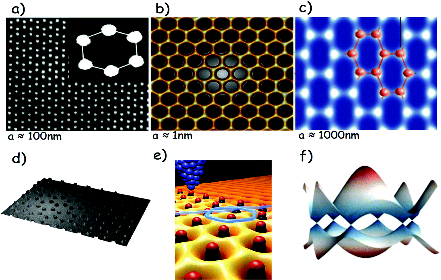 | ||
| Fig. 18 (a) SEM image of AG structure realized by e-beam lithography and reactive ion etching on a GaAs/AlGaAs heterostructure. Electrons localize underneath the nanopillars (white dots; also shown in (d).260 (b) STM topography of a molecular graphene lattice composed of 149 carbon monoxide molecules.259 (c) A honeycomb optical lattice for ultracold K atoms.261 (e) Electron moving under the prescription of the relativistic Dirac equation. The light blue line shows a quasi-classical path of one such electron as it enters the AG lattice made of carbon monoxide molecules (black/red atoms) positioned individually by an STM tip (comprised of Ir atoms, dark blue). (f) Tight-binding calculations of the Dirac Fermion miniband structure of the AGs in (a) and (d). | ||
One of the reasons for pursuing the study of AGs is that these systems offer the opportunity to reach regimes difficult to achieve in graphene, such as high magnetic fluxes, tuneable lattice constants, and precise manipulation of defects, edges, and strain. These can enable tests of several predictions for massless Dirac fermions,265,266 Studies of electrons confined in artificial semiconductor lattices, as well as studies of cold fermions and bosons in optical lattices, may provide a key perspective on strong correlation and the role of disorder in condensed matter science. AG systems might open new avenues of research on spin–orbit coupling, with impact on spintronics, and frontier issues related to novel topological phases.
These are centred on TIs,267–269 that have emerged as a promising class of materials in this regard.269 Strong spin–orbit coupling results in an insulating bulk and metallic edge or surface states (respectively for 2d and 3d systems). These states are “topological” in the sense that they are insensitive to smooth changes in material parameters, and also exhibit unique spin textures. One remarkable phenomenon is the Quantum Spin Hall Effect (QSHE), which for a 2d TI, consists of pairs of edge counter-propagating modes with opposite spins.112 Meanwhile, the surface state of a 3d TI exhibits spin-momentum locking, where the spin is perpendicular to the electron momentum. The spin texture of these states implies that backscattering by non-magnetic impurities is strongly suppressed, resulting in insensitivity to disorder and long coherence times. Due to this behaviour, TIs are promising for next-generation electronics, as well as for spintronics and quantum computing.270 The QSHE effect was first predicted in graphene,112 linked to the honeycomb topology of the lattice112 and to the contribution of a weak spin–orbit coupling.112 AG structures in systems properly engineered to display large spin–orbit coupling represent viable candidates to simulate TI states. There are further possibilities for research arising from the demonstration that single atoms can function as atomic-size gates of a 2d electron system at noble metal surfaces, whereby simple molecules, such as CO, function as repulsive potentials for surface electrons when shaped into open and closed quantum structures. Individual CO molecules arranged on Cu(111) were used as a tuneable gate array to transform a 2d gas of electrons moving through these lattices (Fig. 18).201
Control over every lattice position and potential would result in control of the spatial texture of the hopping parameter, ultimately allowing observation of electronic ordering into ground states, rarely encountered in natural systems. In AGs, molecular graphene, artificial lattices in semiconductors, and optical lattices of cold atoms, controlled densities of ‘artificial impurities’ can be introduced259 in otherwise perfect lattices. Studies of these artificial structures may provide insights on localization and μ degradation in graphene.
Semiconductor AG may also challenge current thinking in ICT, revealing new physics and applications of scalable quantum simulators for ICT based on semiconductor materials already used in real-life electronic and optoelectronic devices. Due to the embryonic nature of the field, any future activity will be high-risk, but has great potential for discoveries. In semiconductor materials the efforts should be directed to the realization of artificial lattices with small lattice constants and with tuneable amplitude, V0, of the potential modulation. The idea is that the energy range, Δ, in which the bands are linearly dispersing in AGs depends on the hopping energy, therefore this quantity is expected to exponentially increase as we reduce the lattice constant and/or decrease the amplitude of the potential modulation. One target could be the realization of AGs in the regime in which Δ approaches 1 meV. This requires lattice constants ∼20–40 nm (see Fig. 19).
 | ||
| Fig. 19 (a) AG Minibands (energy is in meV) with a lattice period a = 60 nm, r0 = 0.2a (r0 is the width of the potential well) and V0 = 5 meV. A dash-dotted line is drawn at the Dirac-point energy. (b) Energy width, Δ, of the linear part of the spectrum near the Dirac point as a function of a. V0 is varied correspondingly (see the right vertical axis) in order to obtain an isolated Dirac point, i.e. without any other state inside the bulk BZ at the Dirac-point energy. Inset: magnification of the energy bands in panel (a) around the Dirac point energy. The blue dashed lines mark the energy limits of the linear dispersion approximation. Adapted from ref. 260. | ||
One ambitious goal is to observe the dispersive intrasubband plasmon mode of the AG lattice by resonant inelastic light scattering or far-IR spectroscopy. Peculiar to plasmon modes in graphene, in fact, is the specific dependence of energy on electron density: ωplasmon(q) ∝ n1/4q1/2, where q is the in-plane wavevector.272 The difference with the classical square-root dependence n1/2q1/2 of 2d parabolic-band systems is a consequence of the ‘relativistic’ linear dispersion of Dirac fermions,273,274 The manifestations of Dirac fermions are particularly striking under the application of a perpendicular magnetic field.275 In AGs with lattice constant much smaller than the magnetic length (a ≪ lB = ħc/eB) this is expected to lead to graphene-like Landau levels.
Such peculiar energy level structure, and the resulting anomalies in QHE experiments,145,146,148 have been largely explored in graphene276 where the lattice constant is a = 0.14 nm (lB ≈ 25 nm at 1 Tesla). Tight-binding calculations show that the Dirac Fermion physics occurs when lB/a > 1.275 In AGs with a ∼ 10–20 nm, a Dirac-Fermion Landau level structure is expected for magnetic fields of several Tesla. In molecular AG structures with a ∼ 1 nm, Dirac Fermion physics should emerge at much smaller magnetic fields. The occurrence of such phenomena can be investigated by conventional QHE and by optical spectroscopy. For lB/a < 1, commensurability effects, such as the Hofstadter butterfly,277–279i.e. a fragmentation of the Landau levels structure, begin to emerge and compete with the Dirac-Fermion physics of the honeycomb lattice.280 These effects prevail when lB ≪ a. The impact of the Hofstadter physics on the energy spectrum of a 2DEG in semiconductor heterostructures was studied in magneto-transport in a lateral superlattice of anti-dots arranged in a square geometry.280 Moiré superlattices arising in SLG and BLG coupled to h-BN provide a periodic modulation with length scales ∼10 nm enabling experimental access to the fractal Hofstadter butterfly spectrum.278,279,281 If met, these demanding limits will enable the occurrence of the physics linked to artificial massless Dirac fermions at T above liquid He. Finally, the impact of e–e interaction can be studied theoretically by exploiting advanced methods such as density-functional theory (DFT) and developing a Kohn–Sham DFT coded for 2d electrons moving in a model periodic potential (see Fig. 20)282 and experimentally by optical, transport and scanning probe methods. Additionally artificial topological order and spin-split counter-propagating edge channels can be pursued by creating honeycomb lattices in 2DEGs confined in InSb and InAs heterostructures, with a large spin–orbit coupling. In this area, the long-term vision is the establishment of a new field of quantum information processing and scalable quantum simulations based on nanofabricated AGs in high-μ semiconductor heterostructures.
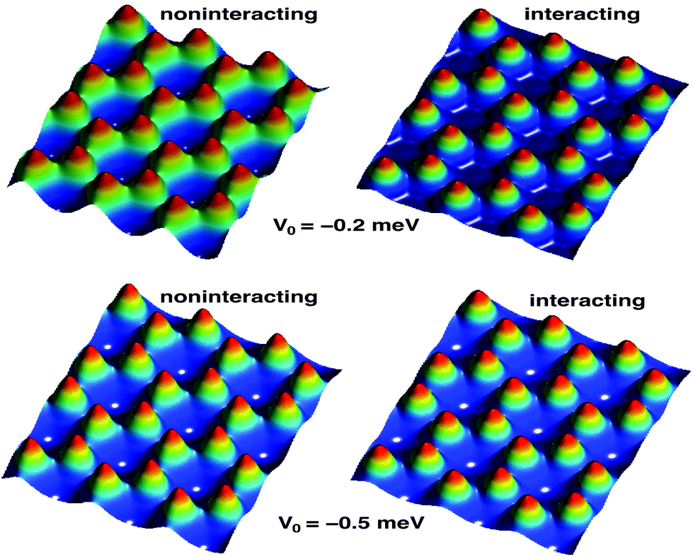 | ||
| Fig. 20 Spatial distribution of electrons in AG (with one electron per pillar) calculated for two values of the potential well representing the pillar. The left and right panels show the results without and with e–e interactions.282 | ||
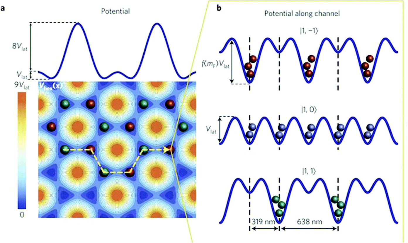 | ||
| Fig. 21 (a) Lattice potential with alternating π+ (green spheres) and π− (red spheres) polarization. The upper plot shows a cut through the 2d potential. (b) 1d potential along the channel of the orange dashed line in (a) for particles in different Zeeman states.284 | ||
A system of spin-polarised fermionic 40K atoms in honeycomb optical lattices was realized in ref. 261, where the presence of Dirac points in the energy spectrum was measured by momentum-resolved detection of the energy gap between bands. A controlled deformation of the hexagonal lattice was used to control the Dirac cones, moving them inside the Brillouin zone (BZ) and eventually merging them.
Besides the perfect knowledge of the potential landscape, this “atomic” approach to the simulation of AG has several additional advantages. Tuning interactions between particles with an appropriate choice of atoms or with Feshbach resonances285 (i.e. scattering resonances that occur when the energy of an unbound state of a two-body system matches that of an excited state of the compound system, see e.g.ref. 282,285,286), allows studying different interaction regimes, from ideal Dirac Fermion physics to strongly-interacting Mott–Hubbard physics. Multi-layer systems can be produced with an additional optical lattice in the orthogonal direction to the 2d honeycomb plane, with an adjustable tunnel coupling between the layers, which could allow the investigation of artificial BLG/FLG. Other interesting perspectives arise from the introduction of artificial magnetic fields for effectively-charged neutral atoms and spin–orbit coupling, which enrich the possibilities of Hamiltonian engineering in ultracold atomic systems.266
Several detection techniques can be used to probe the properties of atomic AG, including measuring transport of atoms across the lattice, even with single-atom (electron) imaging resolution. The excitation spectrum of the system can be directly measured with inelastic light scattering (Bragg spectroscopy),287 which gives access to the dynamical structure factor, while correlation functions of different order (1st order: phase correlations, 2nd order: density–density correlations) can be probed in time-of-flight experiments.286
In addition, a unique feature of ultracold atom experiments is the possibility of changing the lattice and interaction parameters from one experiment to the other, and even modifying them in real time, inducing rapid changes in the AG Hamiltonian enabling the investigation of non-equilibrium dynamics, which can give important information on the system properties.
Of particular relevance is the possibility to study the impact of disorder, which can be introduced in a controlled way by using additional inhomogeneous optical potentials, created e.g. with optical speckles or multi-chromatic optical lattices,288 see Fig. 22. This allows the investigation of the interplay between disorder and Dirac Fermion physics. An example related to 1d optical lattices is shown in Fig. 23, where the different images show the size of an ultracold cloud of non-interacting 39K Bose-condensed atoms for different evolution times and Δ: as Δ increases, the atom cloud stops expanding, becoming Anderson-localized.263
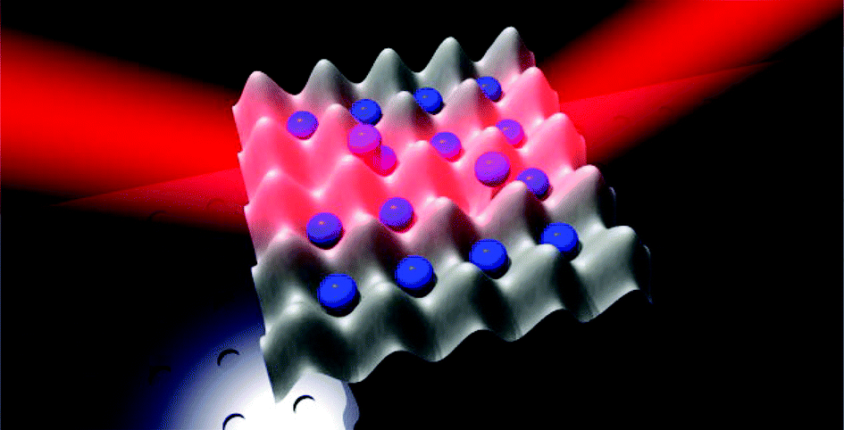 | ||
| Fig. 22 Schematic depiction of ultracold atoms trapped in artificial crystals produced by the interference of laser beams (optical lattices). | ||
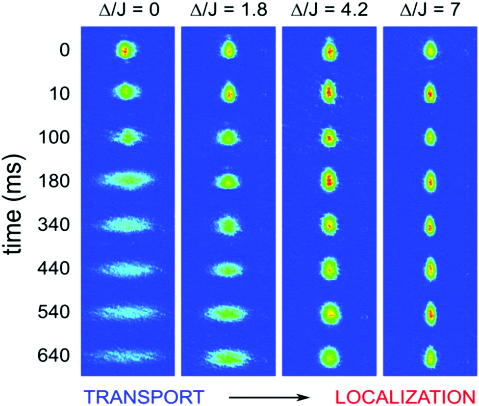 | ||
| Fig. 23 Localization transition for 39 K ultracold atoms in a quasiperiodic bichromatic lattice: as Δ is increased the atomic cloud becomes Anderson-localized.263 | ||
2.7. Atomic scale technology in graphene and patterned graphene
Tailoring electronic and optical properties in graphene can be achieved by lateral confinement of its 2d electron gas from the mesoscopic regime down to the molecular scale,289–295 The dominant approach consists in using inorganic resist to lithographically define GNRs,296,110,297,298 A resist-free approach can be achieved by focused ion beam lithography,299,300 However, the transport in ion-etched GNRs is strongly dominated by edge disorder and amorphization299–302 which calls for alternative approaches. Ultrasonically shredded graphene,303 carbon nanotube opening,304,305 AFM and STM tip-induced oxidation,306,307 and catalytic particle cutting,308–310 offer promising routes to 50–500 Å wide GNRs, but only the former has so far led to functional devices. 40 nm-wide GNRs grown on SiC have shown ballistic conductance on a length scales >10 μm,100 see section 2.7.1.The ultimate goal of graphene-based nanotechnology is to achieve atomic-scale fabrication through techniques that are rapid enough to bridge the gap with standard nanofabricated features. A promising strategy should probably exploit electron and/or scanning probe microscopy techniques. A challenging objective is to investigate the suspended vs. supported cases and, in the latter, define the most suitable atomically flat substrate. However, chemical approaches should also be considered, either from the molecular synthetic or colloidal etching viewpoint. Next, atomic-scale imaging, such as STM, non-contact AFM, aberration-corrected HRTEM, should be developed in the specific realm of atomic-scale graphene devices. Electron transport, optical measurements and local, near-field measurements should be pushed to the limits to assess the properties in atomic-scale devices and identify the degrees of freedom able to control graphene behaviour, such as magnetic field, gate effects, optical excitations, near-field coupling to metallic surfaces, etc. These experimental issues should be guided by a theoretical description and simulations, in particular regarding the bridging between atomic/molecular scale and the mesoscopic regime.
To achieve patterning of GNRs and bent junctions with nm precision, well-defined widths and predetermined crystallographic orientations, STM lithography should be further improved. The latter can be used only for the demonstration of operational principles of new devices, since it should be difficult to incorporate it into a production line, despite the good stability and reproducibility even under ambient conditions307,321 The short de Broglie wavelength [∼0.5 nm] of He ions300,322 gives He ion lithography an ultimate resolution better than 0.5 nm,322 very attractive for GNRs300,323 Using 30 kV He ions, clean etching and sharp edge profiles, ∼15 nm GNRs were obtained, with little damage or doping,323 so that He-techniques may be considered further for GNR production. While many of the promising applications of graphene do not require precise nanoscale processing, there exist numerous applications, e.g. in digital nanoelectronics and spintronics, for which the precise engineering of GNRs307 or antidot lattices324 is mandatory. This is a challenging task, as the properties of GNRs and other graphene nano-architectures depend strongly on the crystallographic orientation of edges,142 the width,325 and the edges atomic structure,326 including edge disorder.142 Precise, reproducible and fast patterning is fundamental for mass production of devices.
Patterning of graphene not only concerns the removal of material (anti-dot lattices, nanomesh, and GNRs) but also suspending it on supports, holes or gates. To date, only few nano-processing methods327,328 have been reported to meet the very strict criteria for nanopatterning, i.e. crystallographic orientation control and atomic scale precision, see Fig. 24. These rely on local probes (STM, AFM) see Fig. 24, or crystallographically selective chemical reactions, or their combinations.
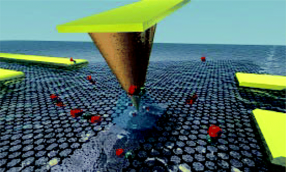 | ||
| Fig. 24 AFM lithography of graphene.306 | ||
The usual method for the production of patterns on the 10–100 nm scale is e-beam lithography, followed by plasma etching. Several groups have used this technique to make GNRs,206 single electron transistors (SET)329 and FETs.330 To open a practically relevant band gap, graphene must be patterned to critical dimensions in the range of a few nm. However, 20 nm is on the threshold of what can easily be achieved using conventional e-beam lithography, due to known electron scattering effects in common e-beam resists.331 Other top-down approaches, such as reduction of graphite oxide,681 unzipping of carbon nanotubes (CNTs)304,332Fig. 25a, or liquid-phase exfoliation (LPE)303 of graphite (Fig. 25d,e), have so far lacked control over the size and edge structure.
 | ||
| Fig. 25 Top-down fabrication of GNRs via (a) CNT unzipping332 (b) STM lithography (adapted from ref. 307), (c) catalytic hydrogenation, using thermally activated nickel nanoparticles, (d) exfoliation of chemically modified328 and (e) expanded graphite662 (i.e. with larger interlayer distance than graphite due to intercalation of nitric337 and sulfuric acid338). Bottom-up fabrication: (f) chemical synthesis336 (g) schematic diagram of GNRs grown on SiC.100 (h) STM image of GNR edge showing helical edge structure.100 | ||
A high precision control of graphene edges could create narrow constrictions, down to the atomic size contacts,333,334 and this enables one to operate a GNR as a quantum wire,335 for use in quantum information processing, in conjunction with QDs. Simultaneously, bottom-up synthesis offers an alternative route towards the production of GNRs (see Fig. 25f): GNRs with lengths of 40 nm were reported.336 40nm wide GNR have been achieved on SiC,100 see Fig. 25g,h. In these GNRs, the transport is dominated by two modes.100 One is thermally activated, while the other is ballistic and T independent.100 At RT, the resistance of both modes is found to increase abruptly at a particular GNR length—the ballistic mode at 16 μm and the thermally activated one at 160 nm.100
Another goal is to investigate the effects of patterning on graphene, to fully control the balance between engineering of desirable properties, against introduction of performance inhibiting defects and artefacts. High-resolution (few nm-scale) lithography enables periodic patterns of voids (‘antidots’) and networks of GNRs.339 The transport, microwave, and far infrared (FIR) properties of such systems require a dedicated investigation. While the study of GNR devices and the optimization of their performance will contribute much to the development of graphene-based nanoelectronics (see section 5) and THz plasmonics, progress made towards atomic-scale technology would make graphene a strong platform for non-CMOS approaches to Boolean information processing, by inspiration of the mono-molecular electronics paradigm.340 Transport measurements may suggest new ways to implement Boolean logic into designed, atomically-defined graphene nanostructures.
The advantage of graphene as QD material lies in its reduced dimensionality, therefore large charging energy, which protects the quantised charged state of the dot. This enables SET operation at high T.342 Coulomb blockade effects and size quantization have been observed in GQDs.329,343,344 It is now necessary to achieve full control on GQD-based circuits. Besides a further development of atomic scale technologies on graphene, this also requires understanding of the properties of electronic states on graphene edges (functionalised and with dangling bonds).
An additional possibility to create GQDs130 is related to the unique properties of BLG.126–128,149 In BLG, one can use a transverse electric field created by external electrostatic gates to open a gap, reaching up to 200 meV.126 It has been demonstrated that one can confine electrons in small regions of BLGs using a combination of top/bottom gates, and then operate the charging states of such QDs electrostatically.345,346 Since spin relaxation in high-quality graphene is slow, in the order of 1 ns, see ref. 219, further studies of gap control and electron confinement in gapped BLGs are needed.
Large-scale periodic patterning of graphene may also be done using deposition of nanoparticles, and this would change the high-frequency response of the system, up to the THz range. A superlattice potential can modify the properties of graphene,355–359 The block-copolymer (BC, i.e. a polymer derived from two (or more) monomeric species), technology360 can be used to create “soft” modulations of graphene, in contrast to “hard” modulations caused by the antidots. In particular, we envisage graphene sheets gently suspended on a regular array of “needles”, fabricated with the BC technology. These novel structures may lead to new phenomena arising from the nature of the modulation, and its tunability. Manufacturing and characterisation of patterned graphene flakes is both a challenging and promising direction of fundamental research, requiring a combination of graphene-specific techniques with methods developed for more conventional materials.
2.8. 2d crystals beyond graphene
There are many examples of 2d crystals. A number of studies5,38 have reported exfoliation of LMs to atomically thin layers. These include h-BN, TMDs,111,361–375 and possible TIs such as (bismuth telluride) Bi2Te3, (bismuth selenide) Bi2Se3 or antimony telluride (Sb2Te3).269,376 Other classes of layered material exist. Examples are transition metal oxides (LaVO3, LaMnO3) transition metal trichalcogenides (NbSe3, TaSe3), transition metal chalcogenide phosphides (Li7MnP4, MnP4), and many others. Each class consists of a range of material types, with its own set of properties. Monolayer MoS2 (1L-MoS2) has a direct band gap377 (while bulk 2H-MoS2 has indirect band gap378) that allows optical applications and, when used in a lateral FETs,379 ION/IOFF up to 108.379 This material has excellent electrostatic integrity that allows flexible electronics,380 and may enable 100000 times less power consumption in standby state than traditional Si transistors.379
Concerning digital electronics Mo and W-based dichalcogenides are 2d semiconductors with band gaps ranging from the visible to the near-infrared (NIR), offering serious perspectives for performant FETs.
The fabrication of the first top-gated SL-MoS2 FETs with RT mobilities ∼60–70 cm2 V−1 s−1, large ION/IOFF (∼108) and low sub-threshold swings (74 mV dec−1) were reported in 2011.379 This was followed by studies focussed on understanding381,382 the charge transport regime (mainly variable range hopping) and band transport regime,383 as well as further optimizing the performances of the devices, with the finding that few-layer samples display the best RT μ > 100 cm2 V−1 s−1.384–386 Still, improvement of the device characteristics are needed, as well as improvement on the overall quality of the 2d materials, together with environmental conditions for achieving non-invasive contact and gating, aspects that are strongly driving the current flow and dissipation.387
However, progress towards realization of functional devices is being made with advances in low power electronics,388 photodetectors,389 low frequency noise devices390 and spintronics391 (see also ref. 392 for an additional discussion).
Reduced dimensionality is a great advantage for electronic applications. Quantum-mechanical confinement usually translates into different electronic and optical properties from the bulk. Mechanical properties are also tuned by ultra-thin thickness, and the large surface–volume ratio would certainly affect chemical reactivity. With this in mind, we foresee potential applications in optoelectronics,393 catalysis,394 batteries,395,396 or supercapacitors,397,398 ultrasensitive sensors for pressure changes,399 gas storage or separation, lubricants,400 and many others. Titania nanosheets could be ideal for ultrathin high- dielectrics, with maximum values of ε ≈ 125 for thickness of a few nm,401 better than conventional dielectric oxides,402,403 TMOs, in particular MnO2 flakes, have excellent properties for batteries404 and supercapacitors.405,406 They also have photoelectrochemical properties,407 with photon-to-electron conversion efficiencies comparable to those of dye-sensitized solar cells (DSSCs).408 The small thickness may facilitate charge separation of excited e–h pairs, although the low conductivity could favour recombination, if longer migration distances are required. Electrical conductivity can be enhanced by combination with graphene, which could enable high-performance energy storage flexible devices. Moreover, the good mechanical properties,409,410 of some 2d crystals (i.e. BN and MoS2) make them attractive as fillers to reinforce plastics.411 Thin films prepared from the exfoliation of layered compounds may lead to efficient thermoelectric devices.38,396
Ultrathin films of tin (stanene)117,118,123 and phosphorus (phosphorene),116 see Fig. 26, are gaining attention because they have properties of potential interest for the engineering of new concept nanodevices.412
 | ||
| Fig. 26 Crystal structure of few-layer phosphorene. (a) Side view of few-layer phosphorene. b,c, Side and top views of 1L phosphorene. Adapted from ref. 116. | ||
Calculations have shown that a phosphorene monolayer is a semiconductor with a direct band gap of 0.9 eV,116 with a strong band gap dependence on N.116 Phosphorene has promise for electronics. μ ∼ 286 cm2 V−1 s−1 at RT was reported in Ref. 116. This is lower than its bulk counterpart (black phosphorus) where the e and h μ are ∼1000 cm2 V−1 s−1 at RT413 and could exceed 15000 cm2 V−1 s−1 for e and 50000 cm2 V−1 s−1 for h at low T.413μ could increase significantly upon surface passivation, in a high- dielectric environment.414
The electronic properties of silicene and germanene (the Si and Ge equivalent of graphene) have also been studied theoretically412,415–417 both materials being predicted to be gapless semiconductors with linear energy dispersion relations near the K points, like graphene. Structural, vibrational and electronic structure of silicene and germanene grown on various substrates have been studied using DFT, and found to be influenced by their interaction with the underlying substrate.418 See section 4.14 for the production and processing of these compounds.
The newly found/produced 2d crystals must be subjected to the same exhaustive studies as graphene. Their structure must be tested using TEM and grazing incidence XRD. Some of these techniques require improvements to get molecular-scale information. Of particular interest would be the development of tools sensible to light elements, enabling chemical differentiation. In this sense, recent developments on annular dark-field TEM419 are very promising. It is most natural to determine the electronic band structure of 2d crystals using ARPES. There are several European facilities with capacity to perform such studies, on a massive scale: BESSY (Berliner Elektronen-Speicherring Gesellschaft für Synchrotronstrahlung) in Germany, Diamond Light Source in the UK, SOLEIL in France, DAFNE (Double Annular Factory For Nice Experiments) in Italy, and several others. Since electronic states in transition metal compounds may feature strong spin–orbit coupling, some of the studies will involve spin-resolved ARPES. Moreover, the development of a scanning ARPES instrument with submicron-resolution is highly desirable for speeding up such studies: this will enable the investigation of free-standing monolayers left upon lift-off of a bulk layered crystal, without the necessity to transfer those onto a substrate.
The studies of individual flakes need to be performed using a broad range of optical techniques, in particular, absorption, reflectivity, ellipsometry and luminescence. Raman scattering can probe phonons,204,205 as well as electronic excitations,204,205 and can be used to determine the N.205E.g., the Raman spectrum of bulk MoS2 consists of two main peaks at ∼382 and ∼407 cm−1 (Fig. 27)204 assigned to E12g in-plane and A1g out of-plane modes, respectively.420 The former red shifts, while the latter blue shifts with the number of layers.421 Moreover, they have opposite trends when going from bulk MoS2 to 1L-MoS2, so that their difference can be used to monitor N.421 However, the trends are not fully understood, and more work is needed to clarify the changes with N. Raman spectroscopy of C and LB modes is also a useful tool to probe these materials.2336 These modes change with N, with different scaling for odd and even N.205 With the increase of N, the frequency of the observed C mode of multilayer MoS2 blue shifts, while that of LBMs red shifts,204 as shown in Fig. 27. The C and LB frequencies, ω(N), of a LM with N layers depend on N as follows: (N ≥ 2N0, and N0 is an integer: 1, 2, 3, 4…). This formula can be generally applied to any LM.205
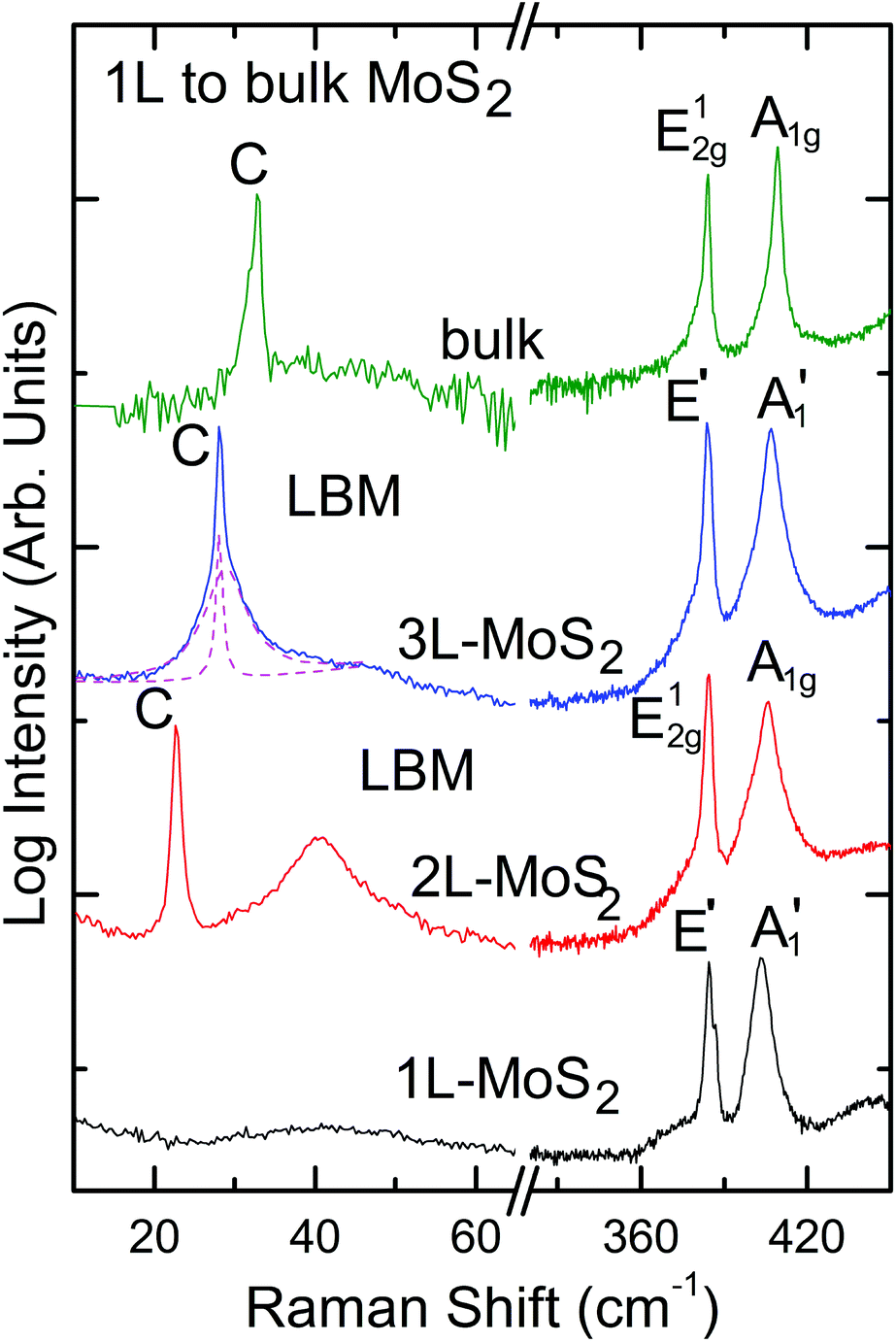 | ||
| Fig. 27 Raman spectra of 1L-MoS2, 2L-MoS2, 3L-MoS2, and bulk MoS2 measured at 532 nm. Adapted from ref. 204. | ||
Metallic NbSe2 and NiTe2 can be studied using FIR and microwaves. Doped LMs can be subjected to FIR magneto-spectroscopy,422,423 to characterise the effective masses and to develop non-contact methods for quality assessment.
Transport measurements (T dependent resistivity, Hall effect) of individual flakes will require the development of methods for non-destructive deposition of metallic contacts and the implementation of the 2d crystals in FET-type devices. These studies may appear to be material sensitive and will require the development of low-T deposition processes: some of the dichalcogenides start losing Se and Te already at few hundred °C.424 Semiconducting 2d crystals, such as MoS2, offer opportunities for low-power electronics. Because of their atomic-scale thickness and lower dielectric constant than in Si, 2d semiconductors offer higher electrostatic control and could overcome issues related to short-channel effects in Si.425
All of the new 2d crystals will need to be investigated using surface scanning techniques, such as AFM and STM. STM studies can shed light onto the spatial structure of the electronic states near the Fermi level, as well as their accessibility from the environment. STM can also provide information on the electronic structure of defects in dichalcogenides (such as S, Se, or Te vacancies) and on the influence of oxygen on these compounds.
2.9. Hybrids of graphene and other 2d crystals
The concept of “materials on demand”: an assembly of graphene and other 2d crystals into hybrid super-structures, Fig. 28, needs to be explored. This would allow the creation of a large number of different multilayers with properties tailored for novel, multitasking applications. From the simulation point of view, there is a need for development of new models of electronic interactions for modelling transport at the mesoscale, effects of disorder, and device simulation. DFT and quantum Monte Carlo simulations can determine the band structure and microscopic charge distribution in monolayers of various TMDs, and CMG. Developments may enable to predict optical properties, electronic correlations, and photochemical reactions, as well as to interpret the experimental findings. Multi-scale approaches such as quantum mechanics/molecular mechanics (QM/MM) can be applied for 2d crystals in solution, or interactions with macromolecules (e.g. for lab-on-a-chip applications that require control on decoration with molecular sensors). New possibilities to find stable TMDs with ferro- and antiferromagnetic properties need to be tested. The electronic properties of monolayers and bilayer of ternary compounds BxNyC1−x−y need to be modelled. This can be done both ab initio, and by developing phenomenological models for the alloy properties. Using the input from the ab initio band structure, minimal tight binding models can be developed for each particular compound, and used to describe their optical properties (see section 2.5). Effective Fermi liquid theories for electrons at low excitation energies for each 2d compounds need to be developed and used to analyse transport and correlation properties, including the Landau level spectrum and transport in the QHE regime. Using DFT and effective low-energy theories, the electronic properties of the edges of the layers and states formed around defects can be studied. These low-energy models, in conjunction with group theory can also be used to model the electron–phonon coupling.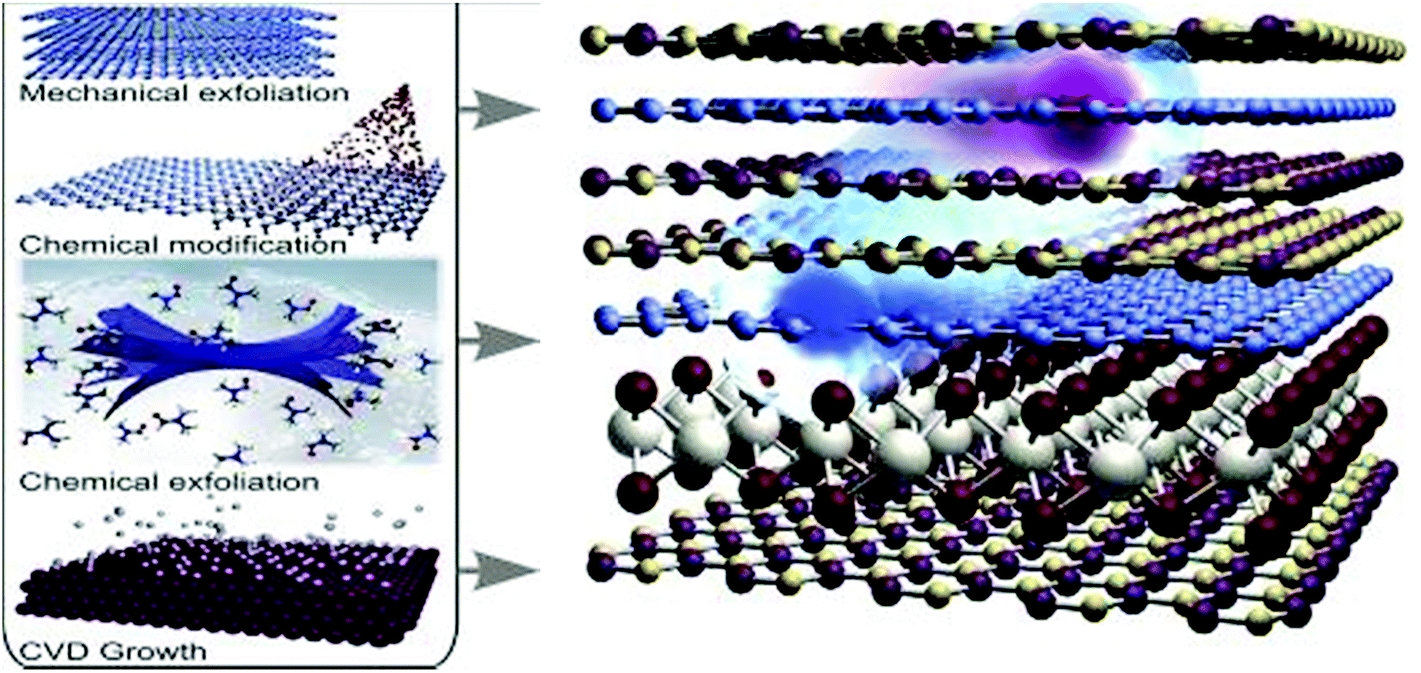 | ||
| Fig. 28 From 2d crystals to superstructures. | ||
2.9.1.1. Tunnelling and resonant tunnelling devices. The feasibility of using multilayer structures for tunnelling devices was demonstrated106 (Fig. 29) showing that BN can act as an excellent defect-free tunnel barrier.106 1L-BN separating two graphene electrodes provides a high-quality tunnel barrier and allows biases as large as 1 V without electrical breakdown.106 The first experiments on exfoliated SLG/BN/SLG structures showed non-linear tunnelling I–V curves,106 see Fig. 30. Several other architectures have been realized with modulated tunnel barriers.434–440
 | ||
| Fig. 29 I(V) characteristics of a SLG/4L-BN/SLG device. Adapted from ref. 106. | ||
 | ||
| Fig. 30 Graphene field-effect tunnelling transistor. (a) Schematic of the proposed devices. (b) The corresponding band structure with Vg = 0. (c) The same band structure for a finite Vg and zero Vb. (d) Both Vg and Vb are finite. The cones illustrate graphene's Dirac-like spectrum. Adapted from ref. 106. | ||
Theoretical understanding of transport properties of such vertical FETs, leading to the full control of their operation, will require a substantial dedicated effort. One challenge is to develop a quantitative microscopic description of single-particle tunnelling processes, based on atomistic approaches. The other is to take into account several factors important for different parts of the I(V) spectrum: orientation mismatch of SLG flakes, contribution of phonon-assisted inelastic tunnelling, and defect-assisted tunnelling.
Aiming at practical applications, further investigations are needed to explore vertical tunnelling structures of graphene, h-BN and materials from the TMD family in various nonlinear electronic elements, such as frequency multipliers. Tunnelling experiments are the first steps towards the production of other devices, as they will allow finding optimum thickness and learning about achievable quality of one-atom-thick barriers.
There are various types of devices where quantum tunnelling may be used (e.g. tunnelling magnetoresistance devices or resonant tunnelling diodes). Atomically thin, smooth and continuous barriers offered by the use of 2d crystals can improve quality and characteristics of any existing or considered scheme involving quantum tunnelling. Investigation of resonant tunnelling is a logical continuation of the tunnelling experiments. Modulating the tunnelling barrier height by using different materials (e.g. heterostructures like SLG/h-BN/MoS2/BN/SLG or SLG/h-BN/SLG/BN/SLG) may create additional states in the barrier, which would allow resonant tunnelling, see ref. 106. Such devices are most interesting to get negative differential resistance conditions, useful for various non-linear components. Resonant tunnelling through impurities and defects enables to map the wavefunction of the latter.441
Vertical graphene-based structures represent a new approach to develop functional electronics. Rapid response and ultra-small sizes could be achieved in vertical transistors. Indeed, electron transfer through nm thick barriers can be extremely fast (and, possibly, coherent). Ballistic tunnelling transistors may allow one to overcome the most significant drawback of GFETs: the low ION/IOFF. However, performances achieved to date are poor: ION/IOFF is smaller than 20, while the delay time is four orders of magnitude larger than that expected from ITRS.12 The tunnelling devices would have a highly insulated off state with no dissipation, which should allow not only individual transistors but integrated circuits at RT.442 The latter is difficult to achieve for horizontal transport in graphene and remains a distant goal. The ideas currently under consideration include several architectures for tunnelling/hot electron transistors. The simplest is metal/h-BN/SLG/h-BN/SLG, where the metal contact (separated from the bottom graphene by thick, tunnelling non-transparent h-BN) serves as a gate and two SLG (acting as emitter and collector) are separated by thin h-BN layer. The operation of the device relies on the voltage tunability of the tunnelling density of states in graphene, and of the effective height of the tunnel barrier adjacent to the graphene electrode. It is interesting to experiment with several different dielectrics in heterostructures, such as metal/h-BN/SLG/MoS2/SLG. Higher quality heterostructures and dielectrics with smaller tunnelling barrier might bring ION/IOFF to 105–106, as required by modern electronics.
Another interesting idea is to attempt the development of a hot electron transistor, similar to those discussed in semiconductor electronics.443 Few-atom-thick transistors based on a 2d tunnelling barrier and graphene may allow much better quality, and become more successful in applications. The transit time through such sandwiches is expected to be ≪1 ps,443 whereas there are no limits for scaling down in the lateral dimension to true nm sizes. In a metal/h-BN/SLG/h-BN/SLG system, the thickness of the active part of the devices would be less than 10 atoms (∼3 nm) and should allow a ballistic current controlled by the central graphene electrode. The assembly of 2d crystals into superstructures may allow stacks of several transistors in series (metal/h-BN/SLG/h-BN/SLG)N in a vertical integrated architecture.
2.9.1.2. Light emission and photovoltaics. Superstructures of 2d crystals can be used to develop tunnelling LEDs and photovoltaic cells. Here, we refer to superstructures composed of two conducting layers separated by a barrier with a modulated profile. Quantum wells are one example of heterostructures made by joining, directly at the atomic level, different materials, usually in layers.444,445 A fundamental experimental quantity is the “band offset ratio”, i.e. the ratio of the difference in conduction band energies to the difference in valence band energies.444,445 Heterostructures for which the difference in the band gap energies is largely dominated by the conduction band offset are called “Type I” quantum wells.444,445 Those where e and h have their lowest energies in different materials are called “Type II” quantum wells.444,445 Type-I quantum wells (Fig. 31) can be used for injecting e/h, with subsequent recombination leading to light emission.
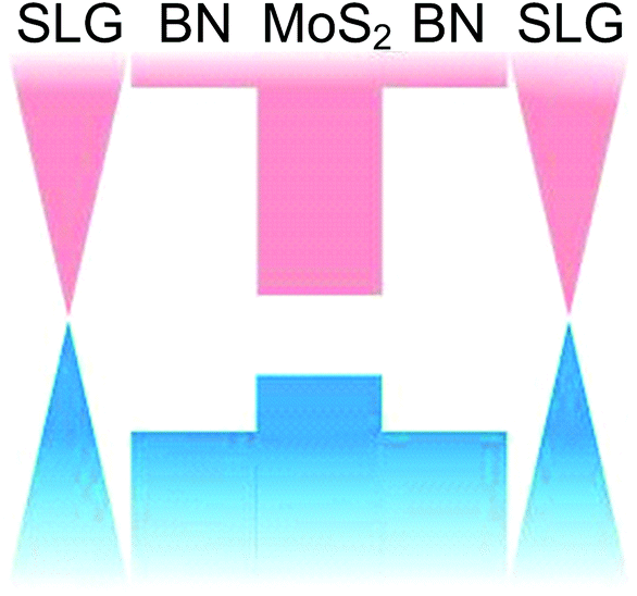 | ||
| Fig. 31 SLG/h-BN/MoS2/h-BN/SLG structure: blue is the valence band and pink is the conduction band. Adapted from ref. 106. | ||
Using more complicated structures, both type-I and type-II quantum wells of various configurations can be created. As the band-structure of 2d crystals depends on N, by changing the thickness of one component, one could tune the optical properties. Using various thicknesses of different materials one can target LEDs of different colours. As individual heterostructures can be combined in one stack with individually contacted layers, LED at different wavelengths could be combined in one structure.
Similarly, PV devices may be created by placing two metallic 2d crystals (e.g. graphene) within tunnelling proximity of each other. By applying a bias (or by exploiting the proximity effect of other metallic 2d crystals) electric field could be created inside the barrier. Any e–h pair excited by light will be separated and contribute to photocurrent.106 Similarly to the case of LED, it should be possible to create heterostructures with various band gaps, sensitive to photons of different energies. Moreover, plasmonic nanostructures can improve the performance of graphene photovoltaic devices.446
2.9.1.3. In situ characterization methods. Hybrid systems will require advanced characterization, which should involve both high spatial and/or point resolutions and coupling, preferentially in situ. This will limit the contact with air, preventing contamination. Two kinds of in situ coupling are worth considering: (i) coupling several characterization methods to investigate a single object, e.g. HRTEM + Raman spectroscopy + electrical measurements, in order to accurately correlate the structural features and the physical behaviour. (ii) Coupling one or several characterization methods (e.g., HRTEM imaging and electrical measurements) with one or several treatment methods (e.g., mechanical and/or thermal stresses) in order to correlate the variation of the behaviours with the structure changes. Considering in situ TEM experiments, the above could be achieved by using sample holders equipped with various facilities (e.g., able to apply thermal or mechanical stresses). However, there is the need to develop other sample holders that will allow a larger panel of possible tests to be applied to the samples under study. When the in situ coupling is technically difficult (e.g., coupling TEM and UV-Raman, which cannot be done through an optical fiber, or coupling TEM and high magnetic field inducer), a chip-based sample holder technology will be highly preferred. Indeed, the latter will allow the chip to be transferred from a characterization system to another, each of them equipped with the appropriate sample holder bearing the same in situ treatment methods. This will allow various investigations on the same samples under the same conditions.
The chemical functionalization of graphene with reactive molecules and the deposition of supramolecular assemblies require studying the self-organization process and the molecule/graphene interface in several conditions: At the liquid–solid interface, by wetting–dewetting processes, but also in connection with ultra-high vacuum (UHV) conditions. This is already possible with UHV systems combining several sources of molecule deposition (sublimation, liquid-valve injection), with surfaces characterization techniques such as STM and X-ray and UV Photoelectron Spectroscopy. Several STM techniques are currently used: low temperature STS, Spin-polarized STM and Fourier-Transform Scanning Tunnelling Spectroscopy (STS), which can allow a local dispersion and surface Fermi measurement. Synchrotron sources can be used for high resolution ARPES, X-ray magnetic circular dichroism (XMCD) and also spin-polarized low-energy electron microscopy, particularly useful for the ferromagnet/graphene interfaces.
2.9.1.4. Hybrid structures for active plasmonics. Combinations of 2d heterostructures with plasmonics would allow for creation of active optical elements. 2d heterostructures are ideally suited to be used with plasmonic structures, as they can be positioned exactly at the maximum of electric field. Such elements are of great importance in different areas of science and technology: from displays, to frequency modulators. Despite great progress, active optics still relies heavily on either liquid crystals,447 which guarantee deep modulation in inexpensive and small cells, but are quite slow,448 or non-linear optical crystals,449 which are fast,450 but bulky and expensive.450 Thus, inexpensive, fast and small active optical elements would be of considerable interest.
The target is the design and fabrication of a new generation of active plasmonic metamaterials with optical properties electrically controlled by 2d heterostructures. Plasmonic metamaterials of various configurations could be achieved by sandwiching between SLG/h-BN heterostructures (see Fig. 32). The conductivity of graphene can be changed by at least two orders of magnitude with electrostatic doping.451 This could modulate the optical properties of the under-lying plasmonic structure. The combination of 2d heterostructures with plasmonics could result in fast, cheap and small active optical elements.
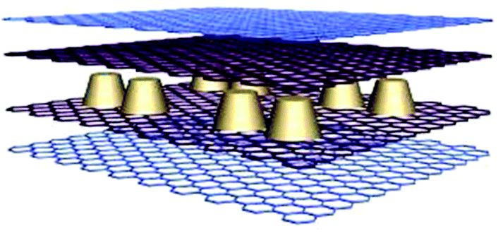 | ||
| Fig. 32 Active plasmonic structure: Au dots sandwiched between SLG/h-BN layers. | ||
2.10. Multiscale modelling of graphene-based structures and new 2d crystals
The optimisation of active plasmonic materials will require multiscale modelling of their properties, taking into account plasma modes and single-particle excitations, as well as their coupling with flexural vibrations of individual layers. Further studies should include modelling of heating of superstructures and their cooling by lateral and vertical heat transfer.Modelling of physical properties of new 2d crystals and hybrid devices constitutes an important research direction. A specialised effort is needed to provide timely interpretation of the characterisation of new 2d crystals, assessment/prediction of functional properties, and guidance of technological effort in creation of hybrid structures (‘materials on demand’, see section 4.15). This will require the implementation of a multiscale modelling approach, in which the materials band structure and local microscopic parameters computed using ab initio simulations are incorporated in the mesoscale description of electronic transport, thermal, mechanical, and optical characteristics, which then enter into the finite-element modelling of operational devices or technological processes.
Many fundamental questions are open in the field of nano-electronics and new materials. Due to the complexity of both, these cannot be answered by conventional simplified approaches. The research of novel functional materials is highly interdisciplinary covering the domains of chemistry, material science, physics, and engineering with their methods and scope of length scales. Advanced knowledge of such fields has necessarily to be combined. In addition, the complexity of quantum laws in nano-electronics complicates upscaling attempts to the point that, at the cross-road of new materials and nanoelectronics (especially for beyond-CMOS applications), only multiscale modelling approaches can progress knowledge sufficiently fast in the near future. The development of the necessary theoretical and computational methods, as well as improvement of the existing technologies, is therefore needed and critical to the STR.
We provide a brief description of the general contours of the various levels of approximations to deal with electron correlations, together with a list of useful codes and a brief technical description of their respective capabilities, in the context of GRM studies. Most common ab initio methodologies encompass the following approaches, all of which will require further development: Hartree–Fock theory (H–F)454 and Post-Hartree–Fock (PH–F)455 quantum chemistry methods. Usually, H–F has insufficient accuracy for most purposes, but it provides a good starting point for quantum chemistry configuration interaction methods, Møller–Plesset456 perturbation theory and coupled-cluster457 methods. PH–F is highly accurate, but scales poorly with system size.458 Such codes generally allow optimisation of geometry and calculation of a wide range of other properties.
DFT is the most “standard” ab initio approach, its main limitation being band gap underestimation.459 Either plane-wave or localised basis sets can be used, but this choice determines the system size that can be simulated. The computational cost of conventional DFT calculations scales with the cubic power of the number of atoms, O(N3), but linear-scaling [O(N)] DFT methods have been developed for insulators.460 DFT results can be mapped to tight-binding, to enable transport calculations (see, e.g., ref. 461, 462). Most DFT codes allow molecular and lattice dynamics calculations. The long standing difficulty to deal with vdW forces463 was recently overcome,464 and several codes, such as AB-INIT or SIESTA (described below) now offer functionals that allow for an accurate description of vdW, a critical issue when dealing with electronic properties of LMs (such as BN/graphene, graphene/graphene, etc.).
GW is the approximation to the self-energy of quasi-particles in a many-body system, to obtain accurate excitation energies.465 The methods generally scale as O(N4) but ref. 466 reported a O(N3) implementation.467 GW can use the Bethe–Salpeter equation468 to describe excitonic effects,469,470 but scaling is O(N6).
TDDFT is the time-dependent formulation of the Kohn–Sham,471,472 equations, to calculate response functions.472 Poles of density–density response function correspond to excited states. TDDFT is cheaper, but less accurate than GW, for determining excited-state energies.
Quantum Monte Carlo (QMC) is the most accurate total energy method for condensed matter physics.473 Scaling is O(N3), like standard DFT, but with a much greater prefactor.473 QMC is able to exploit massively parallel computers. Excitation energies are accurate, but must be calculated one by one as differences of total energy. QMC molecular and lattice dynamics will be available in the near future.
There is a manifold of codes suitable for the study of structures and electronic features of GRMs. Among the most accurate DFT methods, usually based on plane-waves basis set, one can consider AB-INIT, CASTEP, VASP or ADF described below.
AB INITio (ABINIT):474 A package that allows to calculate a broad number of molecular and periodic solids’ properties as total energy, electronic structure and charge density, optimized geometries and dynamic simulations using calculated DFT forces and stresses, dynamical matrices, Born effective charges, dielectric tensors, excited states etc. The programs use codes based on DFT, Density-Functional Perturbation Theory(DFPT), Many Body Perturbation Theory (GW approximation and Bethe–Salpeter equation) and TDDFT.
CAmbridge Serial Total Energy Package (CASTEP):475 a full-featured code based on a first-principles quantum mechanical description of electrons and nuclei. It uses the robust methods of a plane-wave basis set and pseudopotentials.
Vienna Ab initio Simulation Package (VASP):476 a plane-wave all-electron code using the projector-augmented wave method to describe the electron–core interaction. The code uses fast iterative techniques for the diagonalization of the DFT Hamiltonian and allows total-energy calculations and structural optimizations for systems with thousands of atoms and ab initio molecular dynamics simulations for ensembles with a few hundred atoms extending over several tens of ps.
Amsterdam Density Functional (ADF):477,478 A suite based on DFT that uses Slater-type orbitals479 as basic functions to make electronic structure calculations, also able to perform TDDFT. ADF can calculate various molecular properties like IR, Raman, VCD (vibrational circular dichroism), UV and XAS (X-ray absorption spectroscopy) spectra, NMR and EPR (electric paramagnetic resonance) parameters, solvent and environmental effects.
Such methods are limited in terms of system size, and mainly restrict the exploration of material models few hundreds of atoms large. O(N) methods are implemented using localized basis sets, gaining in upscalability but at the cost of a reduced accuracy. Among the most useful: SIESTA, CONQUEST, ONETEP, QUANTUM ESPRESSO, FLEUR, OCTOPUS.
Spanish Initiative for Electronic Simulations with Thousands of Atoms (SIESTA):480 a method and its computer program implementation, to perform efficient electronic structure calculations and ab initio molecular dynamics simulations of molecules and solids. SIESTA's efficiency stems from the use of strictly localized basis sets and from the implementation of linear-scaling algorithms which can be applied to suitable systems. Its accuracy and cost can be tuned in a wide range, from quick exploratory calculations to highly accurate simulations matching the quality of other approaches, such as plane-wave and all-electron methods. VdW interaction has been recently implemented.481
Concurrent O(N) QUantum Electronic Simulation Technique (CONQUEST):482 A linear-scaling code based on DFT, to perform electronic structure calculations on very large systems, up to millions of atoms, with the possibility of choosing different levels of accuracy.
Order-N Electronic Total Energy Package (ONETEP):483 a linear-scaling code for quantum-mechanical calculations based on non-orthogonal generalized Wannier functions,484,485 expressed in terms of periodic cardinal sine functions, in turn equivalent to a basis of plane-waves. ONETEP combines the advantages of the plane-wave approach (controllable accuracy and variational convergence of the total energy with respect to the size of the basis) with computational effort linear with the size of the system.486
QUANTUM opEn Source Package for Research in Electronic Structure, Simulation, and Optimization (QUANTUM ESPRESSO487): an integrated suite of codes for electronic-structure calculations and materials modelling, based on density-functional theory, plane waves, and pseudopotentials (norm-conserving, ultrasoft, and projector-augmented wave). QUANTUM ESPRESSO builds upon electronic-structure codes developed and tested by the original authors of novel electronic-structure algorithms, and applied over twenty years by some of the leading materials modelling groups worldwide.
Jülich FLAPW code family (FLEUR):488 A code designed to calculate properties of solids, based on the Full-potential Linearized Augmented Plane-Wave (FLAPW) method.489
General Atomic and Molecular Electronic Structure System (GAMESS-UK):490 Gaussian-basis quantum chemistry code, with a variety of techniques for PH–F calculations.
OCTOPUS:491 A program aimed at the ab initio virtual experimentation on, in principle, and ever-increasing range of system types. Electrons are described quantum-mechanically within DFT, or TDDFT, when doing simulations in time. Nuclei are described classically as point particles. Electron–nucleus interaction is described within the pseudopotential approximation.
Other methods are more suitable for dealing with dynamical properties of materials, including the formation of stable structures and or the highly accurate description of electron–electron correlations. Those include:
Cambridge quantum Monte Carlo computer program system (CASINO):492 A code based on QMC algorithms for continuum electronic structures calculations using Slater–Jastrow493 pairing, and backflow wavefunctions or combinations of them. It is also possible to extend the range of wavefunctions available.
Cornell-Holland Ab-initio Materials Package (CHAMP):494 A based on QMC algorithms designed to perform electronic structure calculations on a wide variety of systems, such as atoms, clusters, solids, nanostructures and molecules.
Car–Parrinello Molecular Dynamics (CPMD):495 A plane-wave and pseudopotential DFT code designed for performing molecular dynamics simulations, which can be used to perform TDDFT calculations.
CRYSTAL:496 A code designed to compute the electronic structures of periodic systems based on H–F, DFT or hybrid approximations. Atom centred Gaussian functions form the basis set that is linearly expanded into Bloch functions.
The characteristics and fundamental properties of interest for functional materials are co-defined on a larger length scale beyond the ab initio scope. This is because they are additionally influenced by other facts governing properties on such length scales, such as low concentration dopants, impurities or structural defects, or simply because the relevant structures may reach these dimensions themselves. Special attention has to be paid to the interfaces or interaction of layers in multilayer systems.
Multiscale modelling497 is capable of bridging length scales. The concept is based on the observation that not all interactions must necessarily be treated within the first principles framework. This allows one to introduce a hierarchy of interactions, which might be founded either on very general considerations or just adapted and valid for the presently studied properties. Based on this, a hierarchy of levels of treatment may be introduced. The lowest (microscopic) level deals with the smallest objects at the highest accuracy. It can be identified with the full ab initio level. Multiscale modelling defines first the models on each level and second the interfaces for transferring relevant information to the respective upper (or even lower for feedback loop) level, where they are further processed. The advantage is that not all information available on the computationally heavy lower level enters the upper-level modelling, but only relevant condensed information, which is precisely where multiscale modelling benefits from. In addition, modelling of interactions on the upper macroscopic level replaces respective couplings on the more refined lower level. This allows one to reduce the work at the lower level by treating smaller parts (non-interacting subsystems) there. E.g., a finite range impact on electrostatics and on electronic properties can be expected from impurities or dopants depending on the local surrounding of a host crystal. Additional long-range parts such as the Coulomb interaction might be separable and can be treated on the upper level. The information on local electronic properties can still be obtained with massively parallel ab initio methods using large supercells. On the other hand, the evolution of a system as a whole, composed of millions of atoms, including a certain distribution of such dopants, is unpredictable by ab initio methods when the whole system is included at the same level. The problem is solved by combining local ab initio codes with specialised solvers addressing mesoscale range of distances. Such combined codes include:
Learn on the Fly [LOTF]:498 hybrid quantum/classical molecular dynamics which combines quantum-mechanical embedding and classical force model optimization into a unified scheme free of the boundary region, and the transferability problems which these techniques, taken separately, involve. It is based on the idea of augmenting a unique, simple parametrized force model by incorporating in it, at run time, the quantum-mechanical information necessary to ensure accurate trajectories. The scheme was tested on a number of Si systems composed of up to approximately 200000 atoms.499
SMEAGOL:500 DFT-based transport code which calculates transport properties of atomic scale devices, using state of the art electronic structure calculation schemes.
Transport-Spanish Initiative for Electronic Simulations with Thousands of Atoms [TranSiesta]:480 Extension of SIESTA with recursive Green functions solver. The TranSiesta method is a procedure to solve the electronic structure of an open system formed by a finite structure sandwiched between two semi-infinite metallic leads. A finite bias can be applied between both leads, to drive a finite current.
Tight-Binding Simulation [TB_sim]:501,502 tight-binding code which can be interfaced with SIESTA for more realistic descriptions of structures and disorder.503 It is able to compute the structural, electronic, optical and transport properties of various nanostructures.
For a broader range of applications, including electronic and heat transport, optics, optoelectronics, thermomechanics, etc., alternative hybrid codes will need to be developed.
The treatment of disorder deserves particular attention. Indeed, to design a realistic scenario of the influence of disorder on transport properties of materials and devices one has to consider different length scales and modelling strategies simultaneously. First, a microscopic picture of the atomic structure is necessary to access electronic properties. This can only be provided with state-of-the-art first principles simulations. These can be carried out using simple unit cells in clean systems. When considering crystal imperfections or dopants, larger supercells with few impurity atoms or defect sites are necessary.
The interface part is an essential ingredient of the modelling. It defines which information is exchanged, i.e. which features of the ab initio-simulation are strong enough to be important on the macroscopic length scale. From these simulations one extracts electronic structure parameters which represent at best the interactions at this level. For the efficiency of the multiscale approach it is very advantageous if the extracted parameters are generic. This should be considered when setting up the modelling strategy to reduce or, at best, avoid feedback effects. Quantum transport in chemically modified and disordered graphene-based materials can be successfully simulated by means of novel types of O(N) algorithms implemented in the Landauer–Büttiker504 or Kubo–Greenwood505 formalisms (see, e.g., ref. 503, 506, 507). New directions of work should include the effect of spin–orbit coupling, T effects or high bias regimes.
GRM research will greatly benefit from a connection to supercomputers facilities, especially for material simulation to serve as guidance applications. Improvements are required for multiscale modelling and reverse engineering, such as decreasing the problem complexity, ideally to O(N). In DFT this has already been achieved for insulators with the advent of O(N) codes.508 For other methods it is a far greater challenge. Furthermore, it is essential to add functionality (the ability to calculate a range of properties) to these codes, whilst retaining the favourable scaling.
Other improvements include increasing the ease of use (availability of documentation, support, examples, well-designed and clear input and output, ease of installation, etc.), robustness (lack of bugs and numerical reliability), and “reverse engineering” tools to discover the technological principles of a device, object, or system through analysis of its structure, function, and operation.509
Broad cooperation between groups authoring the existing codes is needed, for comparison between codes, for testing and optimisation purposes, development of better interfaces between codes, including better data standards, developments of methods that can exploit massively parallel computer facilities, development of “code libraries” and allowing problems to be distributed among members of a community.
Developments made to first-principles algorithms and codes will be equally useful in other areas of physics, chemistry and materials science. First-principles codes and algorithms aim to be general.
The effects of e–e correlations, as well as the interplay between e–e interaction and disorder can be efficiently addressed using the renormalisation group approach.510 The latter enables one to follow non-trivial (non-linear) scaling of materials parameters upon variation of the length scales at which the electron system is studied. It is based upon the microscopic input (phenomenological or provided by DFT modelling), permitting one to formulate a medium-energy effective field theory describing the physical system, and it is followed by the analysis of the renormalisation flow of essential constants in the theory, which may (or may not) be length scale dependent. The renormalisation group approach can be applied to the studies of both quantum effects, like localisation in graphene, the interactions-driven phase transitions into states with spontaneously broken symmetry, and to studies of classical problems related to the renormalisation of flexural deformations.
The development of efficient methods of kinetic theory is also necessary, in order to treat graphene in strongly non-equilibrium conditions. As a thin material with a weak coupling to the substrate/environment, graphene may easily overheat.511 Moreover, the energy relaxation of non-equilibrium carriers in graphene (photoexcited or injected by tunnelling) requires extensive modelling effort.512,513 Tackling graphene at high current, reaching breakdown, is a more challenging theoretical problem, which requires the use of a combination of the microscopic dynamics computation with the mesoscale kinetic theory.
Apart from fundamental questions, a deeper understanding is relevant for potential applications, because of possible bandgaps induced by correlations that may compete with gaps in graphene nanostructures due to their spatial confinement.
The role of electronic correlations in GRMs is still poorly understood, and its full investigation will thus be a major challenge over the next years. e–e interactions might lead to novel, yet unexplored phases, with possible magnetic order or unusual topological properties, due to an expected time reversal symmetry breaking. The interplay between topology and interactions opens a new research field in theory (advanced analytical and numerical techniques, such as Dynamic Mean Field Theory-DMFT-extensions)516 and experimental physics, where novel experimental techniques are required for probing these phases (e.g. Kerr rotation measurements517).
2.11. Graphene for high-end instrumentation
519,520), the sparkling wavelengths for Xe521 when a charge particle passes through, and it is an excellent conductor, which enables the container itself to act as detector.
Another option is to the substitution of graphite as first wall in nuclear fusion reactors (as the Tokamak ITER -International Thermonuclear Experimental Reactor-,522 presently under construction). Graphite is used to prevent the injection of heavy ions523 with a large number of electrons, as impurities into the plasma. These ions are the result of sputtering processes at the reactor walls. Graphite can only provide light C ions as impurities, which translate into lower losses of the plasma energy. Graphite-based thin films, with low Secondary Electron Yield (SEY), a limiting factor for the achievement of high luminosity in accelerators for positively charged particles, have been developed at CERN.524
2.11.2.1. Quantum resistance. Electric resistance measurements in metrology are always referred to the von Klitzing constant (25
812.807449 Ω),150,525 measured in QHE experiments of semiconductors.150 The fact that graphene is an ideal 2d electron system and not only a quasi-2d system, such as that realized in semiconductor quantum wells and heterostructures, paves the way for new applications of QHE phenomena. The existence of a RT QHE in graphene276 demonstrates that the cyclotron gap can be larger than in any other material, since this gap is not limited by higher electric subbands. The combination with ferromagnetic materials may allow RT applications of quantum Hall phenomena, like quantum resistors or dissipationless current transport.526 The peculiarity of graphene that simultaneously p- and n-type regions can be present in one device allows new designs for quantum Hall resistance standards.527
The QHE is observed in graphene at lower magnetic fields and higher currents than semiconductor QHE devices.150 This may enable a new, simpler and cheaper QHE standard of resistance, that would spread to any metrology institutions and calibration benches (Fig. 33). The von Klitzing constant could be measured in graphene and compared to semiconductors, enabling validation of the von Klitzing relation150 with a quantum Wheatstone bridge,528 a circuit made of two series arrays of two Hall bars parallel to each other.
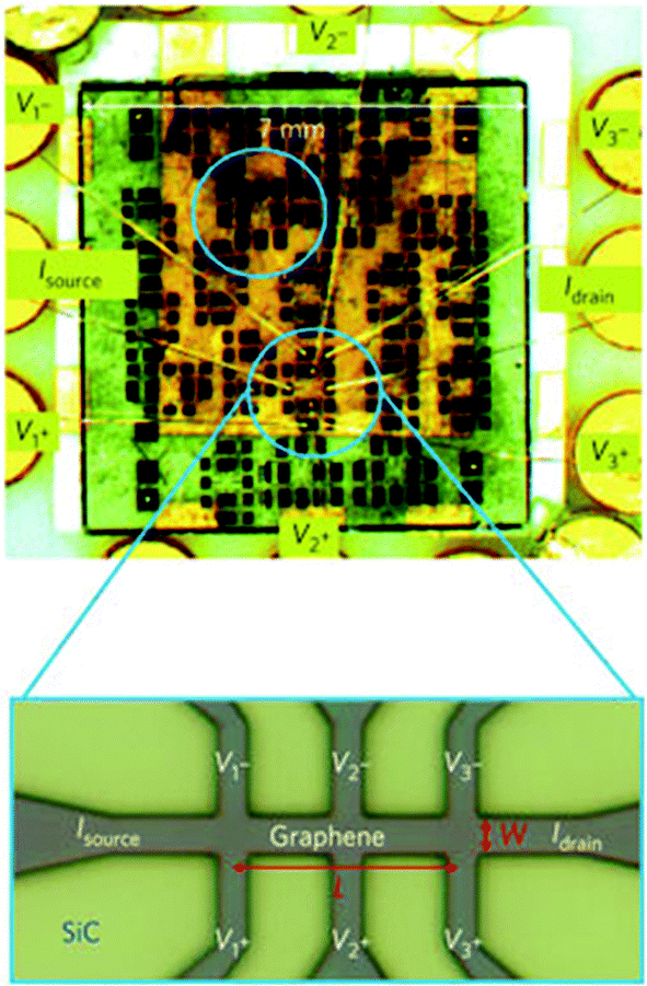 | ||
| Fig. 33 7 × 7 mm2 wafer of SiC with 20 Hall bar devices. The contact configuration for the smaller device is shown in the enlarged image.154 | ||
2.11.2.2. Quantum current standard. Due to the robust Coulomb blockade in GQDs, those can be used in SET nano-circuits.329,343,344 When driven at high-frequency, such SETs can be operated as single electron turnstiles,529 which pass exactly one electron charge per each external field cycle. This enables a fundamental current standard based on charge quantization.329,343,344
2.11.2.3. Standard for optical absorption coefficient. Another use of graphene in metrology is as a standard for the optical absorption coefficient (≈2.3% for SLG in visible light990). It is for some time now that CNTs are used in radiometry530 and photometry.531 The useful property in photometry is the high absorption in a broad spectral range, from UV to IR and THz. CNTs are, therefore, interesting as coating in thermal detectors, and this enables the measurement of optical power in spectral regions where there are no detectors based on semiconductors.532 The extension of these applications to graphene is the next step.
2.12. Perspectives
Fundamental and blue-sky studies of GRMs have a twofold aim. First, the fundamental mechanisms that determine and may limit their potential in already foreseen electronic and optoelectronics applications should be uncovered. Second, the next generation of GRM-based nanostructures for the development of electronic devices beyond CMOS needs to be developed. Research is needed to gain in-depth understanding of microscopic properties of defects in crystal graphene, GBs in polycrystalline graphene, or the influence of environment (such as various substrates), all factors jeopardizing the performances of mass-produced devices. The engineering of electrical circuits incorporating GNRs and GQDs will be essential to exploit the new functionalities of graphene in high-end instrumentation and metrology.154 The study of 2d crystals beyond graphene5,38 is also key to enhance graphene's properties by combining this material with monolayers of 2d crystals in superstructures, which will allow broadening of the range of functional applications of graphene and hybrid superstructures in post-CMOS electronics.The objectives foreseen in the next few years are:
• To establish the fundamental limits for functional graphene nanostructures in electronics beyond CMOS.
This can be achieved via microscopic characterisation of single- and poly-crystalline graphene and graphene-based nanostructures, studies of kinetic processes, influence of defects, disorder, and influence of substrate/environment on electronic properties.
• To explore the use of LMs in electronics.
This will include microscopic characterisation of electronic properties of 2d crystals, studies of their transport and vertical tunnelling properties, and multi-scale modelling of graphene-based and hybrid structures.
The long-term objectives are:
• To exploit graphene for both classical and quantum information processing in the post-CMOS era.
For classical information processing, the development of vertical transistors and atomic scale metal–semiconductor field effect transistor (MESFETs) where graphene is used as active component, as interconnect, or transparent gate is a key objective. For quantum information processing, the exploitation of the long-lived spin coherence of electrons in graphene is needed to develop monolayer and bilayer QD qubits, readouts, and their scalable circuits.
• To build graphene-based metrological applications and high-end electronic instrumentation.
For metrology and standardisation, it is fundamental to develop transferable table-top quantum resistance standards based on the quantum Hall effect, and stable quantised current sources. High-end instrumentations will include highly sensitive bolometers, ultra-sensitive Hall probes, and new types of scanning probes.
• To produce new inorganic 2d crystals, systematically investigate their physical properties, and evaluate the potential for optoelectronic applications.
Using the experience developed with graphene, the long-term vision is to explore a broad range of LMs beyond graphene. The issues that need to be addressed will include material stability, compatibility with nanofabrication processes, and the entire range of structural, optical and electrical characterisation.
• To study electronic, optical, and thermo-mechanical properties of hybrids combining graphene with various 2d crystals.
The microscopic charge transfer and transport in multilayer hybrid structures, optical processes and hot carrier dynamics, electron spin memory and relaxation need to be studied. Understanding these processes will enable the development of devices such as transistors and switches, LEDs, PV cells and photo-detectors.
The timeline is shown in Fig. 34. Timescales: 2–3 years: understanding fundamental kinetic processes and influence of defects. 4–7 years: Understanding of electronic, optical, and thermo-mechanical properties of hybrid structure combining graphene with various 2d crystals that have electronic bandgaps and establishing their fundamental limitation. 7–10 years: Integration of vertical hybrid devices and development of graphene-based metrological systems and high-end electronic instrumentation.
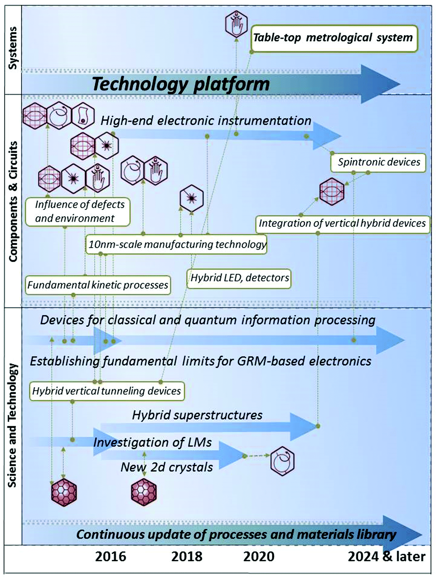 | ||
| Fig. 34 Timeline for fundamental research and development of materials and components. Key technological targets for the three main areas: Science and Technology, Components & Circuits and Systems (reported on Y axis). The forecasts for when the targets are predicted to be met can be read on the X axis. The horizontal arrows indicate the time evolution of each specific target, while the dotted lines indicate how specific targets are linked or are necessary for others inside the same or different STR area. The symbols indicate the involvement and/or the benefits of/for other themes and/or applications. | ||
3. Health and environment
Nanosafety, defined as all the safety issues associated with nanotechnology, is crucially required to translate any future development of new nanotechnologies into action, from industrial applications to health care approaches.533–536 GRMs are not devoid of possible risks on health or environment, and cannot be excluded from these two domains of investigation. It is of fundamental importance to explore the level of toxicity and to establish, if required, constrains for safety of use.537–542The GRM small size and unique physico-chemical properties may pose potential health and environment risks. Determining and resolving safety and toxicity issues will not only be beneficial for integration into devices, but also in light of possible biomedical applications, such as direct nano-interfacing devices with cells and tissues.
Initial studies have assessed the in vitro and in vivo toxicity of graphene and graphene oxide (GO), while for other 2d crystals very little has been done to date. Some of these studies showed that there are no particular risks for using GRMs, conversely others have evidenced that some forms might become a health hazard.537–542 When manipulating a nanomaterial, inhalation is one of the possible ways of contact. Some GRMs have aerodynamic size that may lead to inhalation and deposition into the respiratory apparatus with implications on the formation of granulomas and lung fibrosis.543 On the other hand, the possible biological effects and responses can differ depending on the chemico-physical properties (i.e. N, lateral size, stiffness, hydrophobicity, and surface functionalization), the administered dose and the purity. Limited data542 are available on the difference in biological behaviour between large (few micron lateral size) and small (few hundred nanometer later size) sheets of graphene, or SLG versus FLG. These aspects certainly deserve thorough studies.
3.1. In vitro impact
Ref. 544 reported that graphene induces stronger metabolic activity than single-wall carbon nanotubes (SWNTs) on neuronal cells. Signs of cell membrane damage associated to necrosis (i.e. damage resulting in the premature death of cells in living tissues and organs),545 apoptosis (i.e. programmed cell death induced by biochemical events that lead to changes on cell morphology)546 and reactive oxygen species (ROS), generated in a concentration and time dependent manner, were measured.544 The comparison between graphene and CNTs indicates544 that the shape of the material plays a primary role in determining its biological effects. Ref. 547 tested GO and carboxylated GO (i.e. GO after acid treatment to generate more COOH groups) on monkey kidney cells. At a concentration of 25 μg ml−1, GO accumulated mainly at the cell surface provoking significant destabilization of the cytoskeleton (i.e. the cellular scaffolding contained into the cytoplasms that plays an important role in intracellular and cellular division).547 Carboxylated GO was instead internalized by the cells, accumulating in the perinuclear region, without affecting the morphology of F-actin filaments (a protein, found in all eukaryotic cells, that forms microfilaments).547 GO affected the cell viability at 50 μg ml−1, while carboxylated hydrophilic GO was not toxic up to 300 μg ml−1.547 The lack of a careful definition of the materials (e.g. calling pristine graphene what is instead GO) creates confusion when cytotoxic profiles of different nanocarbons are to be compared. Other studies on different cell lines reported dose and time dependent GO effects on cell viability only at concentration above 80 μg ml−1,548–550 and changes in cell morphology only after long time culturing.551Ref. 552, 553 reported that GO induced time and concentration dependent cell mortality, as documented by the early and late presence of apoptotic cells.To expand the analysis of the cellular responses induced by GO, sheets of different lateral sizes (i.e. 350 nm and 2 μm) were tested.554 Two phagocytic cell lines (i.e. with the capacity of engulfing solid particles) were able to internalize nano-sized and micro-sized GO.554 Little differences on cell viability were observed up to 20 μg ml−1.554 However, the presence of manganese as contaminant, due to inaccurate purification procedures during the oxidative process to prepare GO, induced a GO-independent high cell death.554 This shows how accurate purification steps are relevant in avoiding false positives, that might be erroneously associated to an undesired effect of the nanomaterial itself. In addition, in the phagocytes tested, the uptake and sub-cellular localizations of the two GOs of 350 nm and of 2 μm, were different. The larger GO sheets induced also a stronger inflammatory response. The different behaviours of the two types of GOs can be exploited on different biomedical contexts. The high inflammatory responses of micro-sized GO (2 μm) can be used to promote adjuvant effects (that modify the effect of other agents) in vaccine systems to strengthen weak immune responses. The low inflammatory profiles associated to nano-sized GO (350 nm) can be useful for applications in cancer therapy, where improved biocompatibility is necessary. The study of the effects on macrophages (i.e. cells of the immune system capable to phagocytose, i.e. engulf and digest, cellular debris and pathogens555) was then extended to graphene dispersed in 1% surfactant (Pluronic F108).555 In this experiment, murine macrophages underwent apoptosis through decrease of mitochondrial potential and ROS increase. To identify the mechanisms that trigger macrophage apoptosis is important as it provides information to develop strategies to control cell death induced by graphene. Besides Pluronic, other polymers were shown to improve the biocompatibility of GO and RGO.556
In developing graphene and GO as therapeutic delivery systems of molecules via systemic administration, it is important to evaluate their interaction with blood cells.557,558 When tested, both graphene and GO showed little haemolysis (i.e. rupturing of red blood cells) (max. dose of 75 μg ml−1).557 Haemolytic activity was completely suppressed by coating GO with the polysaccharide chitosan.558 In addition, platelets exhibited normal morphology and were not activated or aggregated. The coagulation pathways were also not influenced, predictive of low risk of thrombosis once intravenously administered. However, two additional studies reported opposite results and evidenced potential thrombotoxicity risks of GO.559,560 These cytotoxic effects were modulated by reducing the carboxylic functions of GO with thermal annealing,559 or by transforming them into ammonium groups.560 This second transformation led to a new modified GO with no effect on platelet stimulation, nor lysis of erythrocytes (i.e. red blood cells) and absence of thromboembolysis (i.e. embolisms due to blood coagulation). What is unclear is the efficiency of the transformation of the carboxylic groups into amines as GO contains also other types of oxygenated functions that should not undergo the chemical transformation following the Curtius rearrangement (i.e. transformation of the carboxylic groups into amines),561,562 applied to GO. When GO was treated with hydrazine to generate RGO, it was highly cytotoxic, lowering cell viability.549
Alternatively to the reduction with hydrazine, other chemical strategies were used to modify GO. Covalent modification with polyethylene glycol (PEG) chains (PEGylation) had the effect to modulate the cytotoxic effect on a series of cell lines, without affecting cell viability up to 100 μg ml−1.563,564 Cytotoxicity of GO was also reduced by functionalization with dextran, a biocompatible polymer widely used for surface coating of biomaterials.565
Ref. 566 carried out a biocompatibility assessment of both CVD and LPE graphene using cultured human lung epithelial cell line A549. No detectable changes in the cellular morphology of A549 cells growing on graphene thin films or cells exposed to graphene flakes (0.1 to 5 μg mL−1) for 4 to 72 h was observed.566 In contrast, the same work outlined how carbon black is significantly more toxic than graphene.566
This set of results represents a significant first step towards the experimental assessment of the in vitro toxicity of graphene and GO. However, to avoid the generalization often found for other carbon-based nanomaterials, such as CNTs,539 it is necessary to take into consideration the great variability of the materials tested. It is essential to compare graphene and GO as well as other GRMs and correlate their impact on cells to their physico-chemical characteristics and, in case, to the chemical changes introduced.
3.2. Cytotoxicity effects on graphene-coated surfaces
The evaluation of the cytotoxic effects of graphene and GO has also important implications on their use as support for tissue regeneration, cell growth, cell differentiation, and for the development of implantable devices (Fig. 35).567,568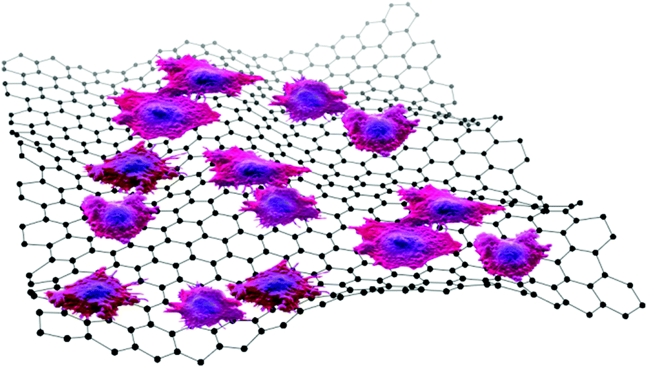 | ||
| Fig. 35 Schematic representation of cells (coloured in purple and with their nucleus in blue) in contact with a surface of graphene (represented as black balls and sticks). | ||
Preliminary studies already explored graphene ability to interface neurons.569 Mouse hippocampal cells were cultured on a graphene substrate to test if the neural functions were affected during their development and maturation in vitro.569 The results revealed high biocompatibility of such growth surface, with low toxicity in the absence of morphological changes.569 The potential use of graphene in neuronal interfacing thus represents a promising approach in future developments of neural prosthesis. Similarly, different surfaces covered by graphene were also able to induce progenitor cell differentiation.570 In particular, graphene allowed to control and to accelerate the proliferation of human mesenchymal stem cells (i.e. multipotent connective tissue cells that can differentiate into a variety of cell types). Cell viability was maintained and no change in cell morphology was observed during the differentiation process, which was enhanced in the case of the cells in direct contact with graphene in comparison to other types of surfaces, like glass or Si wafers.570 This study represents an interesting example where bone regeneration can be achieved in the absence of growth factors, usually required to boost this process.570 It also hints at the safety of graphene when it remains intact after cell growth. This opens the possibility of actively integrating it into devices design to favour tissue regeneration or repair.
3.3. In vivo impact, biodistribution and pharmacokinetics
Additional studies investigating toxicity in vivo,559,560 complemented those in vitro,559,560 directed to assess the impact of GO at the cellular level. Intravenous administration of GO in mice elicited blood platelets aggregation and extensive pulmonary thromboembolism.559,560 This behaviour was associated to the presence of charged functional groups on GO, as the aggregation properties were significantly lowered, when it was chemically transformed into RGO.560In vivo toxicity of GO was evaluated in mice and rats following intravenous administration after labelling with a radiotracer.571 Significant pathological changes, including inflammatory cell infiltration, pulmonary aedema and formation of granulomas were found at a dose of 10 mg kg−1.571 These results were confirmed by another study in which GO, injected in mice, induced granulomas in lungs, spleen and liver.553Pulmonary toxicity is a major concern in the industrial production of nanomaterials, as their volatile nature favours inhalation and might directly cause acute damages and long term diseases. It was reported572 that GO provokes severe and persistent injury in mice lungs following direct injection into the organs.572 However, this form of toxicity was reduced when graphene was dispersed in a surfactant (i.e. Pluronic).572 In another study,543 the exposure risks of the respiratory system were also suggested for graphene nanoplatelets (25 μm lateral size) dispersed in bovine serum albumin.543 Following the inhalation, the nanoplatelets were found to deposit beyond the respiratory tract. Acute inflammatory responses in mice, inflammation and frustrated macrophage phagocytosis (occurring when a phagocyte is unable to engulf its target because it is physically too large) were reported.543 The inflammogenicity (i.e. the ability to sustain long-term inflammatory activity) was attributed to the inhalable aerodynamic diameter,543 an index that determines the respirability of a particle and the site of deposition. The differences in these two studies, both testing graphene dispersed in surfactants, are likely due to the different morphology of the materials used, in terms of N, surface area, dispersion procedures, and/or the presence of contaminants. These parameters can favour variable toxicity profiles. The ability to manipulate graphene's toxicity profile is supported by the evidence that extensively purified GO does not affect polymorphonuclear leukocytes (i.e. white blood cells containing segmented lobular nucleus) even after 7 days of peritoneal administration.573 No giant cells, inflammatory response and granuloma were observed in comparison to pristine multi wall nanotubes (MWNTs).574 The modulation of toxicity in vivo can also be achieved through functionalization. It was reported that GO PEGylation can reduce toxic effects in mice.564
The study of the biodistribution, accumulation and elimination of graphene and GO in vivo is another key step to predict and avoid any user's risk.574,575 Biodistribution studies have shown that GO accumulates predominantly in the lungs,571,574 while low uptake was observed in the reticuloendothelial system – RES (i.e. the part of the immune system that consists of the phagocytic cells located in reticular connective tissue. The cells are primarily monocytes and macrophages, and they accumulate in lymph nodes and the spleen. The Kupffer cells of the liver are also part of the RES).571,574 GO exhibited long circulation time (several hours) in comparison to other carbon forms like CNTs.571,574 While no pathological modifications in the organs were reported after 14 days following the injection of 1 mg per kg of body weight,571,574 significant changes were observed in the lungs at a dose of 10 mg kg−1. PEGylated GO instead accumulated mainly in the tumour of tumour-bearing animals, with lower uptake by RES, without significant toxic effects.574 The same type of material was intravenously injected, after being radiolabelled, to better elucidate the organ biodistribution and the excretion routes.575 Following an initial accumulation in the RES, a gradual elimination was observed between 3 and 15 days.575 After three months, the GO sheets were completely eliminated without toxic effects.575 No signs of abnormality were observed in kidney, liver, spleen, heart and lung.575 This GO was further studied to evaluate more thoroughly the pharmacokinetics and the long-term biodistribution. These parameters were analyzed by radiolabelling the GO with 125I.575 After intravenous administration, the GO sheets were found to accumulate into the RES including spleen and liver.575 They were gradually cleared by both renal and faecal elimination.575 A dose of 20 mg kg−1 did not provoke toxicity in a period of 3 months, as proved by measuring the biochemical parameters in blood, and the haematological markers.575 Histological examination of the different organs did not show damage or lesions, with the exception of an increase in spleen and liver colour intensity due to the accumulation of brown material.575
Similarly to the in vitro tests, many parameters may affect graphene and GO toxicity measures in vivo. The variability of the samples thus far studied is high. Thus, good practice requires to report the morphological and physico-chemical characteristics of each type of tested samples, avoiding generalization, which may introduce strong biases in the final statements on “toxicity” or “non-toxicity”. In essence, toxicity of graphene seems to be associated to its surface functionalization. However, it is necessary to use animal models, and to explore higher doses of material and other routes of administration. These studies will allow understanding the effects of graphene and GO when deliberately administered for therapeutic strategies, or when accidental exposure occurs.
3.4. Bacterial toxicity
Another issue is the toxicity of graphene, GO and RGO towards microorganisms. In ref. 541, 576, 577 different types of bacterial and fungal strains were tested, since any antibacterial activity may be translated into interesting applications in the development of antimicrobial products (see Fig. 36).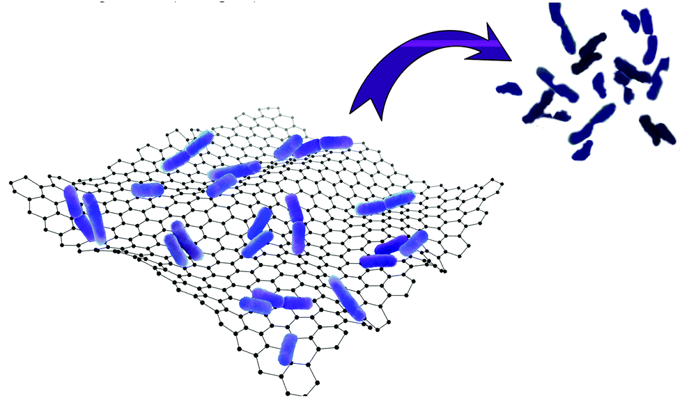 | ||
| Fig. 36 Bacteria (light blue) when in contact with a graphene surface (represented as black balls and sticks) are inactivated (i.e. they lose disease-producing capacity),576 leading to their detachment from the surface, as indicated by the arrow pointing towards the dead bacteria (represented in dark blue).576 | ||
GO and RGO showed antimicrobial activity when tested against Gram-negative E. coli576 (i.e. bacteria that do not retain crystal violet dye in the Gram staining protocol,578 (a procedure named after H. G. Gram in which organisms -bacteria- are differentiated according to cell wall composition, exploiting staining, a technique used to enhance contrast in microscopic images), due to structural properties of their cell walls) and Gram-positive S. aureus577 (i.e. bacteria stained dark blue or violet by Gram staining),576 although RGO was more efficient in inactivating both types of pathogens.577 However, Gram-negative bacteria were more resistant.577 Similar behaviours were observed on E. coli, with GO showing more bactericidal activity.541 Effects on the metabolic activity at different concentrations were complemented by the damage of the microorganism cell membrane, as assessed by TEM.577
To expand further these studies, the antimicrobial mechanism was analyzed using different materials, such as graphite, graphite oxide, GO and RGO.579,580 The higher antibacterial activity was measured for GO,579,580 which had the smallest average lateral size amongst the different types of graphenes.579,580 Direct contact of bacteria with graphene sheets induced a loss of membrane integrity. No ROS generated by superoxide anions (O2−) were detected.579,580 But oxidation of glutathione, a redox state mediator in bacteria, was observed.579,580 These results suggest that the GO antimicrobial action contributes to both membrane disruption and oxidative stress. The physico-chemical characteristics of GRMs seem to play an important role in the efficiency of bacterial killing. These results were questioned by ref. 581 where GO was added to E. coli: bacteria grew faster by forming dense biofilms around GO. Only the combination with Ag nanoparticles induced cell death.581 In view of these results, the bacteriostatic properties (i.e. the ability to stop bacteria from reproducing) of graphene, GO and RGO certainly need further studies. Comparison between the available data is difficult, as the conditions of cell cultures and type of starting materials differ in the various experiments. New studies are thus needed to assess the antimicrobial role as a function of physico-chemical characteristics.
3.5. Biodegradation
The assessment of the bioaccumulation and biodegradation of novel nanomaterials is another fundamental aspect for their safe implementation. The study of the biodegradability of carbon-based materials is of paramount importance to translate their use into new biomedical devices or therapeutic tools, and, in parallel, to anticipate the possible risks when integrated into novel devices. A careful characterization will allow elucidating and clarifying the role of surface modification and its biological impact, eventually proposing solutions for the treatment and use of graphene, improving the knowledge on toxicology, and prospecting it into clinical applications, including therapy, diagnostics and imaging. As recently demonstrated for CNTs,582 GO can undergo degradation by the enzyme horseradish peroxidase in the presence of hydrogen peroxide.583 RGO seems instead more resistant to this enzyme. This has important implications on the design of safer graphene derivatives to minimize the risks for human health and environment.Some microorganisms are also able to modify GO.584 The family of bacteria called Shewanella, which consists of metal-reducing bacteria, was reported to affect GO.584E. coli585 and S. aureus were not inhibited,585 but they were able to reduce GO585 by microbial respiration, providing a unique nontoxic approach to the synthesis and modification of graphene flakes. The mechanism of reduction involved both direct extracellular electron transfer and electron mediators at the interface between cells and flakes. This work should be extended to other microorganisms, not only to modify, but eventually to degrade graphene.
3.6. Environmental impact
To our knowledge, to date there are almost no studies that focus on the ecotoxicity and environmental impact of graphene, GO and RGO.541 The majority of data in literature concerns fullerenes.586 These studies highlight the effect of fullerene ingestion and its associated toxicity in several model organisms: fresh water crustaceans,586 marine copepods586 and fish.586 Several data are also currently available on the ecotoxicological effects of CNTs in various organisms.587 Most studies on CNT ecotoxicity were conducted on representative species of the aquatic environment,588–590 and, to a lesser extent, on terrestrial organisms.591,592 Based on the experience acquired with these carbons, it is mandatory to explore the impact of GRMs on the environment. It is necessary to develop and broaden our knowledge in this area in order to better understand the potential effects on the environment in the short or long term, and to adopt adequate disposal procedures. With the development of graphene technology, it is essential to assess exposure in real-life conditions and to fully understand the graphene life-cycle, otherwise any assessment of occupational or environmental effects will remain uncertain.Thus far, only few studies addressed the influence of graphene on terrestrial plants.593 Phytotoxicity (i.e. toxic effects on plant growth) at concentrations of GO between 500 and 2000 μg ml−1 was studied in cabbage, tomato, red spinach and lettuce.593 Root and shoot growth, biomass, shape, cell death and generation of ROS were evaluated.593 After 20 days of exposure, the plants treated with GO displayed a reduced number of leaves.593 The growth and biomass were inhibited with visible symptoms of necrosis and increased ROS.593 The only exception was lettuce seedlings.593 These effects were dose and time dependent.593 Particular attention needs to be devoted to possible adverse effects of graphene on plant cells. Similarly, GO sheets were tested on the germination of rice seeds in comparison to other carbon nanomaterials such as CNTs and fullerenes.594 While, e.g., CNTs were found to favour an increase in water content during germination,594 GO retarded the development and reduced the water content.594 A possible blockage of the pore seeds by micro-sized GO layers likely caused less water uptake and inhibited germination. This was reflected by a reduced growth of rice seedlings, shorter roots and shoots. The dimensions and form of carbon nanomaterials influence the development of the plants, thus can be of concern during the processes of handling and disposal. In vivo cytotoxicity studies of functionalized GO were performed on zebrafish.594 Zebrafish is one of the model animals for screening the impact of nanomaterials in the environment (since it is a vertebrate, it has a high genetic homology with humans, and the assays can be automated to provide high-throughput along with high-content analysis). Besides analyzing the GO biodistribution and demonstrating the possibility of its use for whole-body imaging, biocompatibility was also assessed.594 Functionalized GO did not induce any significant abnormality on embryonic development,594 nor affected the survival rate, neither provoked malformations.594 To our knowledge, ref. 594 is the first example of evaluation of GO using a relevant model in an environmental context. Although a generalization is impossible at this stage, this can be considered the starting point to intensify the studies in this direction.
3.7. 2d crystals and hybrids
To our knowledge, there are no studies on health and environment impact of other 2d crystals and their hybrids with graphene or other materials. Some studies are available on BN nanotubes595 or cubic-BN.596 BN nanotubes coated with polylysine were tested on a model of muscle cells595 (C2C12 mouse myoblast – an embryonic cell which becomes a muscle cell or fiber-cell line). The tubes are able to penetrate these cells without affecting their viability,595 nor interfering with the formation of myotubes (i.e. multinucleated fibres that form muscle fibres), during cell differentiation.595,596 Alternatively, BN nanotubes were functionalized with dendritic structures bearing carbohydrate ligands to their periphery by non-covalent adsorption.597 The generated complexes interacted with proteins and cells without modifying cell proliferation and viability.597 Morphological alterations in different cell populations exposed to BN nanotubes are cell-type dependent.5983.8. Perspective
Research is necessary to explore the biological responses and the potential toxicity of GRMs looking at their interactions with living systems. This will allow better understanding of the differences between GRMs, eventually establishing a correlation of their impact on health and environment with their physico-chemical characteristics. These studies could guide the safe design, production and manufacturing of GRMs, minimizing health and environment risks. To date, only a few studies focus on the ecotoxicology and environmental impact of GRMs. It is imperative to broaden our knowledge in this area in order to better identify the potential effects in the short and long term. With the development of large-scale production and the arrival on the marketplace, it is essential to assess exposure in real conditions and fully understand the GRM life-cycle. Without this, any assessment of health risks due to occupational or environmental exposure will remain uncertain.The activities on health and environment need to focus on a thorough exploration of the biological responses and the toxicity effects of GRMs by taking into consideration their physico-chemical properties and bio-nano-interactions. The variability between the samples is currently high. The toxicity of GRMs seems to be closely associated to their surface functionalization. In relation to surface characteristics, size is a second important parameter. Other key factors can be also associated to the toxicity of new nanomaterials, such as generation of reactive oxygen species, indirect toxicity because of adsorption of biomolecules or signalling from cells that accumulate nanoparticles to adjacent non-exposed cells (e.g. paracrine signalling599 – a form of cell–cell communication in which a cell produces a signal to induce changes in nearby cells, altering the behaviour or differentiation of those cells), and physical toxicity associated with GRMs interaction with lipids (and other molecules) constituting cell membranes, tissues and organs. In addition, the study of cellular and tissue uptake as a function of GRM size and chemical functionalization is very important. Lateral dimensions of GRMs might affect the population of the receptors involved in the mechanisms of penetration dependent on energy (e.g. endocytosis, an energy dependent process by which cells absorb molecules or nanoparticles by engulfing them, or phagocytosis). If passive processes, as in CNTs,600 happen, it is necessary to understand how the 2d form affects membrane organization (e.g. membrane disruption or sliding between lipid bilayers).601
At the environmental level, the impact on organisms widely used as natural biosensors, such as lichens, and on a certain number of aquatic species, or microorganisms, specifically sentinel species that can be affected once 2d crystals are released, need to be assessed. New living organism models need to be applied to investigate the water/sediment interface and terrestrial behaviour of 2d crystals. All these studies will offer a safer design, production and manufacturing of 2d crystals in order to minimize health and environment risks, Fig. 37.
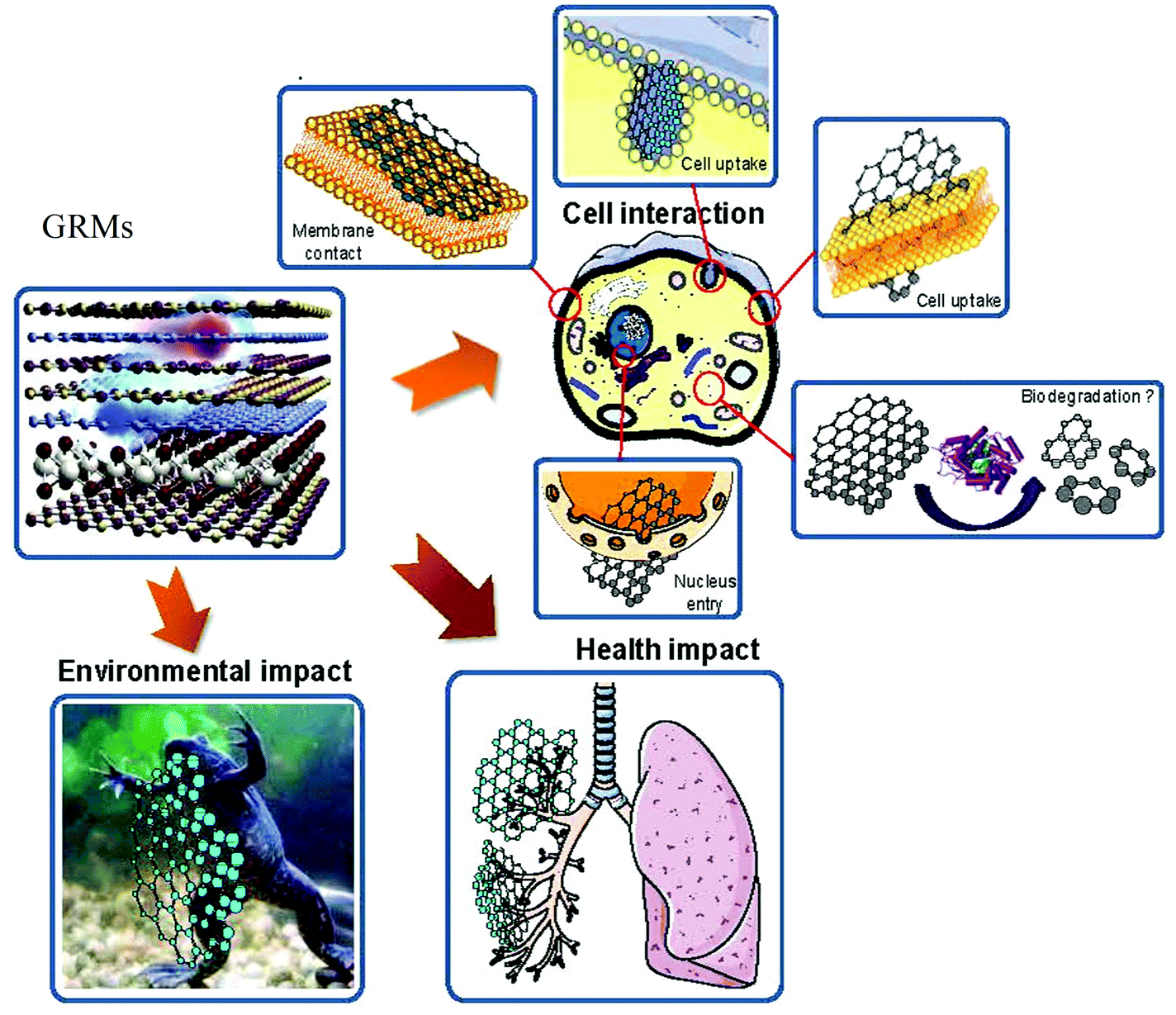 | ||
| Fig. 37 Possible interactions of GRMs with cells, organs (i.e. lung) and living organisms (i.e. amphibian). GRMs can have an environmental impact on living organisms like amphibians as indicated by the left arrow pointing to the frog on the bottom left panel. GRMs can have an impact on human health leading to disease related to respiration, as illustrated by the arrow pointing to the lung (bottom right panel). GRMs can interact at the cellular level as indicated by the top arrow pointing to a cell represented with its subcellular components. Possible interactions of GRMs at the cellular level can occur, following a clockwise direction from the top left panel, at the plasma membrane level (membrane contact), during cell uptake at the cellular membrane (cell uptake), in the cytoplasm where degradation may occur (biodegradation), and at the nuclear membrane (nucleus entry). Adapted from ref. 542. | ||
In this context, several interconnected targets should be pursued: (i) elucidation of how GRMs interact with cells at the cellular and molecular level, with the assessment of the role of the bio-corona (i.e. proteins surrounding a nanomaterial when in contact with a biological fluid); (ii) addressing GRM effects on specific tissues, such as the immune system, nervous system or placenta, and determination of biomarkers for possible pathogenic risks; (iii) identification of any possible GRM hazard in relation to their physico-chemical properties, with a particular focus on the most important exposure routes (i.e. lung, skin); (iv) understanding the processes that control GRM biostability and biodegradation, key to pave the way to nano-interfacing devices; (v) investigation of GRM's potential impact on aquatic species (i.e. amphibians), terrestrial organisms and microorganisms; (vi) development of a standardized and validated GRM testing strategy, to enable regulation.
In the long term, knowledge of GRMs’ biotoxicity and environmental risk will favour: (i) manufacturing, development and applications, (ii) assessment of technological risk versus risk perception to harmonize technical/social visions; (iii) development of tools for the governance of key changes in social landscape for new technology; (iv) converging technologies, i.e. integrative process of orienting S&T capabilities towards societal needs.
The timeline is shown in Fig. 38. Timescales: 2–3 years: Investigation and understanding the effect of GRMs on different cells and identifying possible hazard. 4–7 years: Development of GRMs regulation. 7–10 years: Assessing the impact of GRMs and validation of safety issues for technological development.
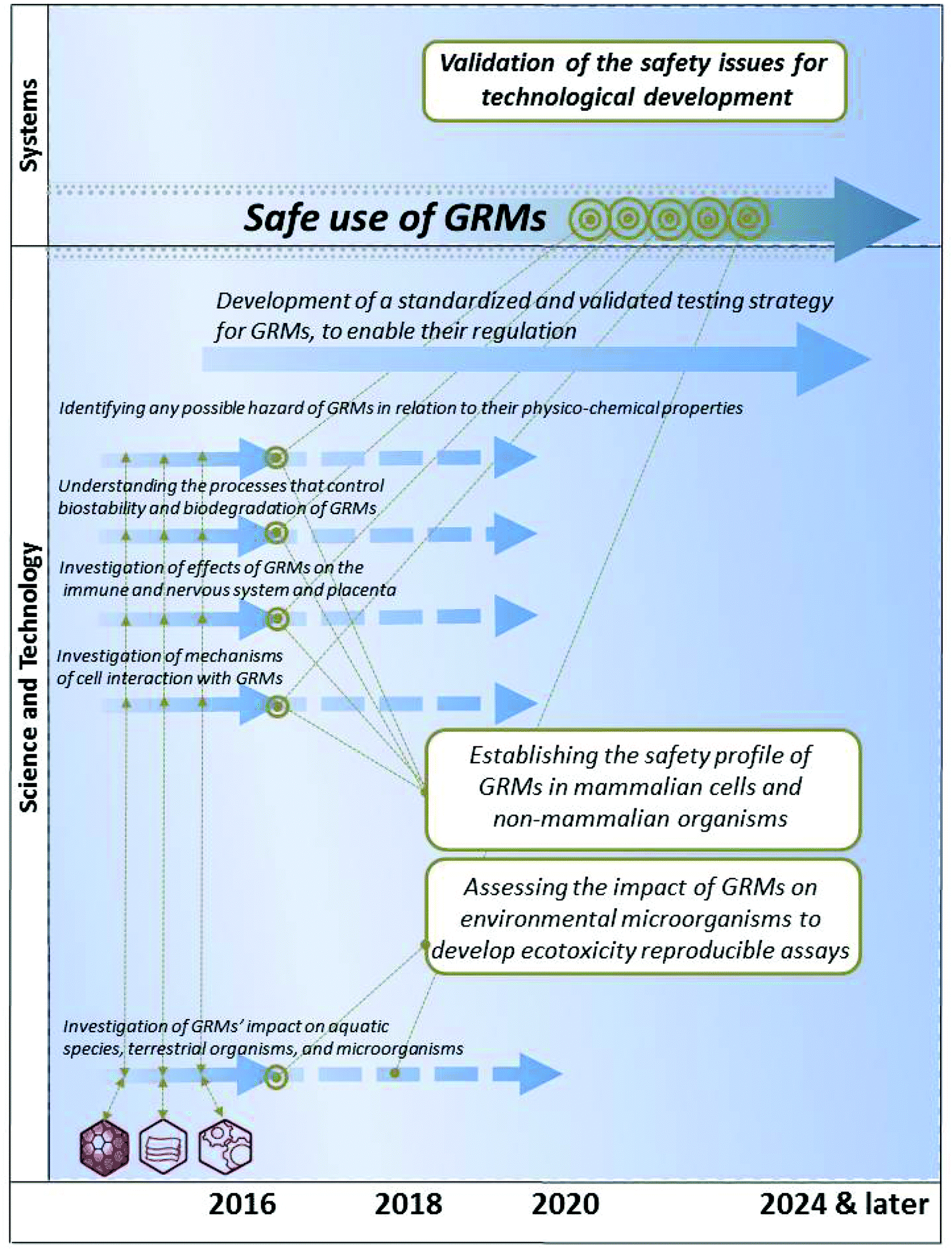 | ||
| Fig. 38 Timeline for the study of impact on health and environment of GRMs. | ||
4. Production
The industrial use of GRMs will require large scale and cost-effective production methods, while providing a balance between ease of fabrication and final material quality, defined as on-demand tailored properties according to the final use. One advantage of graphene is that, unlike other nano-materials, it can be made on large and cost-effective scale by bottom up (atom by atom growth) or top-down (exfoliation from bulk) techniques,602 see Fig. 39. Prior to large-scale production, developing laboratory scale protocols for synthesis with targeted properties is essential.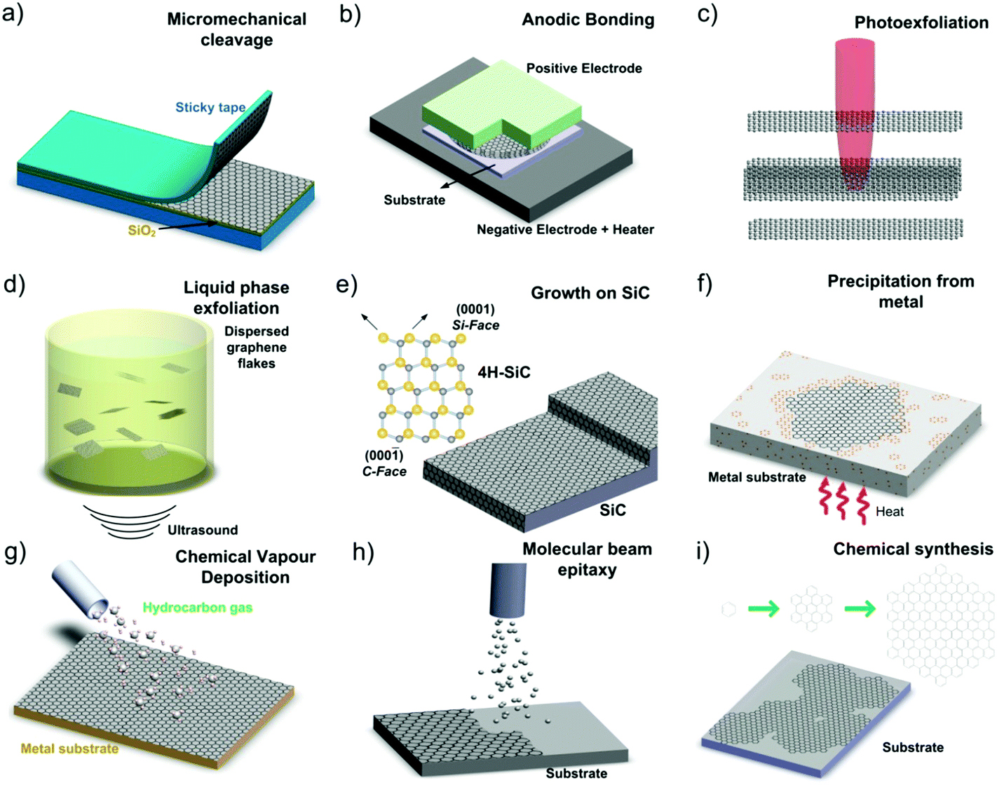 | ||
| Fig. 39 Schematic illustration of the main experimental setups for graphene production. (a) Micromechanical cleavage (b) Anodic bonding (c) Photoexfoliation. (d) Liquid phase exfoliation. (e) Growth from SiC. Schematic structure of 4H-SiC and the growth of graphene on SiC substrate. Gold and grey spheres represent Si and C atoms, respectively. At elevated temperatures, Si atoms evaporate (arrows), leaving a C-rich surface that forms graphene. (f) Precipitation from carbon containing metal substrate. (g) CVD process. (h) Molecular beam epitaxy. Different carbon sources and substrates (i.e. SiC, Si, etc.) can be exploited. (i) Chemical synthesis using benzene as building blocks. Adapted from ref. 602. | ||
The combination of graphene with other materials in heterostructures, as well as functionalization, will play a key role in validating GRMs as a disruptive nanotechnology platform for real-world devices. Table 2 summarize the state of the art in term of size and μ for some of the production strategies presented in Fig. 39, together with targets applications.
| Method | Crystallites Size, μm | Sample Size, mm | μ | Applications |
|---|---|---|---|---|
| Micromechanical cleavage | 1000 | 1 | 2 × 105 cm2 V−1 s−1 | Fundamental research and proof of principle devices |
| 106 cm2 V−1 s−1 | ||||
| (@T = 4 K) | ||||
| 2 × 104 cm2 V−1 s−1 | ||||
| @RT | ||||
| LPE of graphite | 0.01–1 | 0.1–1 | 100 cm2 V−1 s−1 | Inks, coatings, paints, batteries, supercaps, solar cells, fuel cells, composites, sensors, TCs, photonics, flexible electronics and optoelectronics, bio-applications |
| (∞ as overlapping flakes) | (for a layer of overlapping flakes) | |||
| @RT | ||||
| LPE of GO | >1 | >1 | 1 cm2 V−1 s−1 | Inks, coatings, paints, batteries, supercap, solar cells, fuel cells, composites sensors, TCs, photonics, flexible electronics and optoelectronics, bio-applications |
| (∞ as overlapping flakes) | (for a layer of overlapping flakes) | |||
| @RT | ||||
| Growth on SiC | 100 | 100 | 6 × 106 cm2 V−1 s−1 | RF transistors |
| (6′′) | @T = 4 K | other electronic devices | ||
| CVD | 50000 |
1000 | 6.5 × 104 cm2 V−1 s−1 | Photonics, nanoelectronics, TCs, sensors, bio-applications, flexible electronics |
| @T = 1.7 K | ||||
| 3 × 104 cm2 V−1 s−1 | ||||
| @RT |
The main targets are:
• Development of scalable synthesis protocols that enable tuning of electronic, structural and optical properties for different applications.
• Enlargement of scope of GRMs applications by adding new functionalities. This implies developing a strategy for covalent and non-covalent functionalization with molecules, clusters and nanocrystals.
• Systematic exploration of 2d crystals. Hundreds of LMs have not yet been exfoliated and could exhibit interesting properties that would be useful in a range of applications.
• Development of hybrid structures combining graphene and other 2d crystals.
In the short term, it is imperative to meet graphene specifications required by the targeted applications and develop scalable strategies to build graphene heterostructures with improved functionalities. The main long-term goal is to achieve on-demand large-scale heterostructures of 2d hybrid systems, with control of growth, pattern formation, functionalisation and self-assembly, without compromising the quality of the layers.
The production effort should not be limited to lab-scale synthesis, but should also aim at recognizing and understanding the sources of differences in materials properties compared with mechanically exfoliated flakes, as well as improving properties, such as electrical and thermal conductivity, μ, carriers concentration, functionality and homogeneity.
In the short term, these objectives should be targeted:
• Development of scalable synthesis protocols for GRMs. This includes the development of functionalization processes that enable tuning of electronic, structural and optical properties for different applications. This will constitute a breakthrough in GRMs growth technology, paving the way for the production of 2d-based devices on an industrial scale.
• Development of scalable liquid exfoliation synthesis and functionalization of GRMs, optimizing their properties for different applications (energy, composites, electronics, optoelectronics, and bio-medicine). Processing of liquid exfoliated GRMs in ultrathin few layer films. Formulation and characterization of inks suitable for printings and coatings.
• Developing bottom up approaches to grow GRMs from molecular precursors on metals (CVD), (molecular beam epitaxy, MBE), etc., for energy, electronics, optoelectronics and spintronics. Cluster and nanoparticle decoration of graphene films. Optimization of reliable transfer techniques on different target substrates (flexible and non-flexible).
• Development of growth of graphene on commercial SiC wafers, both polarities and politypes, assessing the homogeneity of thickness, maximum carrier μ, concentration and functionalizations. Implementing surface engineering intercalation protocols leading to high μ through intercalation by hydrogen and/or other elements.
• Development of methods to build multistacked heterostructures formed by a few layers that can be the bases of new devices. Hybrids of BN/graphene and graphene/other 2d crystals.
The objectives to be pursued in longer time frames (∼10 years) are:
• Further optimization of specific graphene properties enabling additional applications, among them tailoring GNR bandgaps, increasing μ of graphene grown on metals and SiC, improving the synthetic processes to achieve larger areas. Also, as the synthetic methods progress and reach maturity, implementation of technological processes leading to in situ/ex-situ patterning, continuous growth/synthesis, on-line characterization and continuous, deterministic transfer.
• Production of other 2d crystals whose properties and applications are unknown today. This will determine many activities in the long term, not limited to graphene but enabling a complete exploration of the Flatland promise.
In the following sections we overview the production strategies and processing and placement methods of GRMs, starting with the historical development602 going through the analysis of the state of the art,602 and future goals.
4.1. Graphene production
4.1.1.1. Mechanical exfoliation for research purposes and new concept devices. Micromechanical cleavage (MC), also known as micromechanical exfoliation, has been used for decades by crystal growers and crystallographers.603,604 In 1999 ref. 605 reported a method of cleaving graphite, yielding films of several layers of graphene. Ref. 605 also suggested that “more extensive rubbing of the graphite surface against other flat surfaces might be a way to get multiple or even single atomic layers of graphite plates”. This was then firstly demonstrated, achieving SLG using an adhesive tape, by ref. 5, as for Fig. 39a).
MC is now optimized to yield high quality layers, with size limited by the single crystal grains in the starting graphite, of the order of millimeters.125 The number of layers can be readily identified by elastic (see Fig. 40a)171 and inelastic134 light scattering (Raman spectroscopy, see Fig. 40b). μ up to 107 cm2 V−1 s−1 at 25 K were reported for a decoupled SLG on the surface of bulk graphite,606 and up to 106 cm2 V−1 s−1 on current-annealed suspended SLGs,607 while RT μ up to ∼20000 cm2 V−1 s−1 was measured in as-prepared SLGs.608 Suspended SLGs, cleaned by current annealing, can reach μ of several 106 cm2 V−1 s−1 (ref. 609). μ > 105 cm2 V−1 s−1, with ballistic transport at the micron level, was reported for SLG encapsulated between exfoliated h-BN layers.99
 | ||
| Fig. 40 (a) Optical micrograph of MC flake, with regions of different thickness. (b) Evolution of Raman spectra with N.134 The spectra are normalized to have the same G peak intensity.602 | ||
Although MC is impractical for large-scale applications, it is still the method of choice for fundamental studies. Indeed, the vast majority of basic results and prototype devices were obtained using MC flakes. Thus, MC remains ideal to investigate both new physics and new device concepts.
4.1.1.2. Anodic bonding. Anodic bonding is widely used in the microelectronics industry to bond Si wafers to glass,610 to protect them from humidity or contaminations.611 When employing this technique to produce SLGs,612,613 graphite is first pressed onto a glass substrate, and a high voltage of few KVs (0.5–2 kV) is applied between it and a metal back contact (see Fig. 39b), and the glass substrate is then heated (∼200 °C for ∼10–20 min).612,613 If a positive voltage is applied to the top contact, a negative charge accumulates in the glass side facing the positive electrode, causing the decomposition of Na2O impurities in the glass into Na+ and O2− ions.612,613 Na+ moves towards the back contact, while O2− remains at the graphite–glass interface, establishing a high electric field at the interface. A few layers of graphite, including SLGs, stick to the glass by electrostatic interaction and can then be cleaved off;612,613T and applied voltage can be used to control N and their size.612,613 Anodic bonding was reported to produce flakes up to ∼1 mm width.613 This method may also be used for other LMs.
4.1.1.3. Laser ablation and photoexfoliation. Laser ablation is the use of a laser beam to removal of material, via evaporation and/or sublimation, from a solid surface614, Fig. 39c). In the case of LMs, such as graphite, if the laser beam irradiation does not induce evaporation and/or sublimation of the carbon atoms, but the detachment of an entire or a part of a layer, the process is called photoexfoliation.615
Laser pulses can in principle be used to ablate/exfoliate graphite flakes, Fig. 39c. Tuning the energy density permits the accurate patterning of graphene.616 The ablation of a defined N can be obtained exploiting the energy density windows required for ablating a SLG616 and N-layer graphene (NLGs).616Ref. 616 reported that energy density increases for decreasing N up to 7LG. Ref. 616 argued that the N dependence of the energy density is related to the coupling of heat with NLGs via phonons, with the specific heat scaling as 1/N. For N > 7 the ablation threshold saturates.616 Laser ablation is still in its infancy616,617 and needs further development. The process is best implemented in inert or vacuum conditions,618,619 since ablation in air tends to oxidize the graphene layers.616 Promising results were recently demonstrated also in liquids.620 Thus, photoexfoliation could be alternative and complementary technique to LPE.
Laser irradiation has room for further optimization. This technique was tested to produce flakes from direct laser irradiation of GO.621 New protocols are needed to prepare graphene flakes in liquid, overcoming the limitations of LPE, exploiting high boiling point solvents and surfactants. The laser irradiation approach is of general validity. It can be extended to other LMs with weak interlayer coupling, see section 4.12.2.
The LPE yield can be defined in different ways. The yield by weight, YW [%], is the ratio between the weight of dispersed graphitic material and that of the starting graphite flakes.35 The yield by SLG percentage, YM [%], is the ratio between the number of SLG and the total number of graphitic flakes in the dispersion.35 The Yield by SLG weight, YWM [%], is the ratio between the total mass of dispersed SLG and the total mass of all dispersed flakes. YW does not give information on the “quality” (i.e. the composition of the dispersion, e.g. the presence of SLG, BLG, etc.) of the dispersion, since it considers all the graphitic material (SLG, FLG and thicker flakes), thus it does not quantify the amount of SLG, but only the total amount of graphitic material in dispersion. YM [%], and YWM [%] are more suitable to quantify the amount of dispersed SLGs.
In order to determine YW it is necessary to calculate the concentration c [g L−1] of dispersed graphitic material. c is usually determined via optical absorption spectroscopy (OAS),35,58,624–627 exploiting the Beer–Lambert Law: A = αcl, where l [m] is the length of the optical path and α [L g−1 m−1] is the absorption coefficient. α can be experimentally determined by filtering a known volume of dispersion, e.g. via vacuum filtration, onto a filter of known mass,35,624–627 and measuring the resulting mass using a microbalance. The filtered material is made up of graphitic flakes, surfactants or solvents and residuals from the filter.35,624 Thermogravimetric analysis (TGA) is used to determine the weight percentage of graphitic material, thus enabling the measurement of c.58–61 However, different values of α have been estimated both for aqueous59,60 and non-aqueous-based dispersions.35,626Ref. 35 derived α ∼ 2460 m L mg−1 m−1 for a variety of solvents, i.e. N-methylpyrrolidone, NMP, dimethylformamide, DMF, benzyl benzoate, γ-butyrolactone, GBL, etc., while later ref. 626 reported α ∼ 3620 mL mg−1 m−1 for NMP. Ref. 624 gave α ∼ 1390 mL mg−1 m−1 for aqueous dispersions with sodium dodecylbenzene sulfonate (SDBS), while ref. 627 reported a higher value ∼6600 mL mg−1 m−1, still for aqueous dispersions but with sodium cholate (SC). Ref. 627 assigned this discrepancy to the difference in concentration of the two dispersions. However, α cannot be dependent on the concentration (indeed it is used for its determination), thus more work is needed to determine its exact value.602
Y
M is usually determined via TEM and AFM. In TEM, N can be counted both analyzing the edges134 of the flakes and by using electron diffraction patterns.134 AFM enables the estimation of N by measuring the height of the deposited flakes and dividing by the graphite interlayer distance, 0.34 nm.602 However, the estimation for the height of SLG via AFM is dependent on the substrate.602 Indeed, on SiO2, a SLG has a height of ∼1 nm,5 while on mica is ∼0.4 nm.628 Raman spectroscopy can be used for the determination of YM35,625,629 and to confirm the results obtained with TEM and/or AFM. YWM [%] requires the estimation of the SLGs area other than N.35 Although this is more accurate (giving quantitative and qualitative information on SLGs), with respect YW and YM, its determination is time consuming. However, for a semi-quantitative evaluation, YM and YW must be reported if YWM is not.
4.1.2.1. LPE of graphite. Ultrasound-assisted exfoliation is controlled by hydrodynamic shear-forces, associated with cavitation,630i.e. the formation, growth, and collapse of bubbles or voids in liquids due to pressure fluctuations.630 After exfoliation, the solvent–graphene interaction needs to balance the inter-sheet attractive forces.
Solvents ideal to disperse graphene are those that minimize the interfacial tension [N m−1]631 between the liquid and graphene flakes. In general, interfacial tension plays a key role when a solid surface is immersed in a liquid medium.631–633 If the interfacial tension between solid and liquid is high, there is poor dispersibility of the solid in the liquid.631 In the case of graphitic flakes in solution, if the interfacial tension is high, the flakes tend to adhere to each other and the cohesion (i.e. the energy per unit area required to separate two flat surfaces from contact631) between them is high, hindering their dispersion in liquid.602 Liquids with surface tension (i.e. the property of the surface of a liquid that allows it to resist an external force, due to the cohesive nature of its molecules631) γ ∼ 40 mN m−1 (ref. 35), are the “best” solvents for the dispersion of graphene and graphitic flakes, since they minimize the interfacial tension between solvent and graphene.602 The same solvents have been investigated for the debundling of CNTs.634–636
Ref. 637 determined via wettability and contact angle the surface energy, ϱ [mJ m−2], of different graphitic materials, finding ϱ ∼ 46 mJ m−2, ∼55 mJ m−2, ∼62 mJ m−2 for RGO, graphite and GO. The slight difference being due to the different surface structure of GO, RGO and graphite. Ref. 638 reported that the contact angle measurements are not affected by N.
The majority of solvents with γ ∼ 40 mN m−1 (i.e. NMP, DMF, Benzyl benzoate, GBL, etc.) [see ref. 35 for a more complete list] have some disadvantages. E.g., NMP may be toxic for reproductive organs,639 while DMF may have toxic effects on multiple organs.640 Moreover, all have high (>450 K) boiling points, making it difficult to remove the solvent after exfoliation. As an alternative, low boiling point solvents,641 such as acetone, chloroform, isopropanol, etc. can be used. Water, the “natural” solvent”, has γ ∼ 72 mN m−1,631 too high (30 mN m−1 higher than NMP) for the dispersion of graphene637 and graphite.637 In this case, the exfoliated flakes can be stabilized against re-aggregation by Coulomb repulsion using linear chain surfactants, e.g. SDBS,624 or bile salts, e.g. SC642 and sodium deoxycholate (SDC),250,625 or polymers, e.g. pluronic,643etc. However, depending on application, surfactants/polymers may be an issue, e.g. compromising, decreasing, inter-flake conductivity.644
Thick flakes can be removed following different strategies based on ultracentrifugation in a uniform645 or density gradient medium (DGM).646 The first is called differential ultracentrifugation (sedimentation based-separation, SBS),645 while the second density gradient ultracentrifugation (DGU).646 SBS separates various particles on the basis of their sedimentation rate645 in response to a centrifugal force acting on them. SBS is the most common separation strategy and, to date, flakes ranging from few nm to a few microns have been produced, with concentrations up to a few mg ml−1.626,647 High concentration is desirable for large-scale production of composites35 and inks.629YM up to ∼70% can be achieved by mild sonication in water with SDC followed by SBS,250 while YM ∼ 33% was reported with NMP.629 This YM difference is related to the difference in flake lateral size. In water-surfactant dispersions flakes are on average smaller (∼30 nm250 to ∼200 nm624) than in NMP (∼1 μm35,629), since the viscosity (ν) at RT of NMP (1.7 mPa s648) is higher than water (∼1 mPa s648). Larger flakes in a higher ν media experience a higher frictional force645,646 that reduces their sedimentation coefficient, making it more difficult for them to sediment. This decreases YM in NMP compared to water.
Control on N is achieved via DGU: graphitic flakes are ultracentrifuged in a preformed DGM646,649 see Fig. 41a,b. During this process, they move along the cuvette, dragged by the centrifugal force, until they reach the corresponding isopycnic point, i.e., the point where their buoyant density equals that of the surrounding DGM.646 The buoyant density is defined as the density (ρ) of the medium at the corresponding isopycnic point.649 Isopycnic separation has been used to sort CNTs by diameter,650 metallic vs. semiconducting nature651, and chirality.652 However, unlike CNTs of different diameter, graphitic flakes have the same density irrespective of N, so another approach is needed to induce a density difference: coverage of the flakes with a surfactant results in an increase of buoyant density with N, see Fig. 41c. Fig. 41d is a photograph of the cuvette after the isopycnic separation with Sodium Deoxycholate (SDC). To date, YM up to ∼80% was reported by using isopycnic separation.642
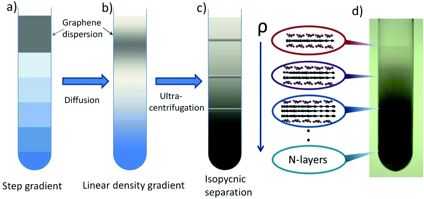 | ||
| Fig. 41 Sorting of graphite flakes via isopycnic separation. Formation of (a) step gradient and (b) linear density gradient. (c)The flake-surfactant complexes move along the cuvette, dragged by the centrifugal force, until they reach their corresponding isopycnic points. The buoyant density of the flake-surfactant complexes increases with N. (d) Photograph of a cuvette containing sorted flakes. Adapted from ref. 602. | ||
Another method is the so-called rate zonal separation (RZS).653,654 This exploits the difference in sedimentation rates of nanoparticles with different size654,655 shape656 and mass,654,655 instead of the difference in nanoparticle density, as in the case of isopycnic separation. RZS was used to separate flakes with different size653 (the larger the size, the larger the sedimentation rate).
Other routes based on wet chemical dispersion have been investigated, such as exfoliation in ionic liquids (ILs),657,658 1-hexyl-3-methylimidazolium hexafluorophosphate (HMIH)657 or 1-butyl-3-methylimidazolium bis(trifluoro-methane-sulfonyl)imide ([Bmim]-[Tf2N]).658 These are a class of purely ionic, salt-like materials,659 defined as salts in the liquid state (below 100 °C), largely made of ions.659Ref. 657 reported concentrations exceeding 5 mg mL−1 by grinding graphite in a mortar with ILs, followed by ultrasonication and centrifugation. The flakes had sizes up to ∼3–4 μm, however no YM data was shown. Ref. 657 used a long ultrasonication process (>24 hours), probably because of the IL high ν. In SBS ν plays a fundamental role. Flakes in a higher ν medium have a lower sedimentation coefficient with respect to water. The sedimentation coefficient is commonly measured in Svedberg (S) units (with 1S corresponding to 10−13 s), i.e. the time needed for particles to sediment out of the fluid, under a centrifugal force.79E.g., for a flake dispersed in [Bmim]-[Tf2N] (ρ = 1.43 g cm−3, ν = 32 mPa s), the sedimentation coefficient is ∼55 times smaller than in water.602 There are no reports to date showing that exfoliation via ultrasonication in ILs can have the same YM as in water,250 or organic solvents.629 Moreover, the resultant flakes contain oxygen functional groups,658 probably due strong non-covalent interactions, or covalent functionalization with [Bmim][Tf2N] itself.658 A step forward for the production of flakes without these functional groups was reported in ref. 660 where oxygen-free flakes were made by grinding graphite in 1-butyl-3-methylimidazolium hexafluorophosphate, [BMIMPF6]. ILs were then removed by mixing with Acetone and DMF.658 Controlling grinding time and IL quantity, ref. 658 reported GQDs with size from 9 to 20 nm and thickness between 1 and 5 nm.
Alternative processes rely on exfoliation of fluorinated graphite,661 expanded graphite,662 and non-covalent functionalization of graphite with 1-pyrenecarboxylic acid.663
LPE is cheap and easily scalable, and does not require expensive growth substrates. A range of applications for graphene lie in conducting inks629 (Fig. 42a), thin films35 (Fig. 42b) and composite materials624 (Fig. 42c). For these, graphene is best prepared as flakes, so that the active surface is maximised. The resulting material can be deposited on different substrates (rigid and flexible) following different strategies, such as drop and dip casting (Fig. 42d), rod (Fig. 42e) and spray coating (Fig. 42f), screen and ink-jet629 printing (Fig. 42g), vacuum filtration,35 Langmuir–Blodgett,662 and other techniques.
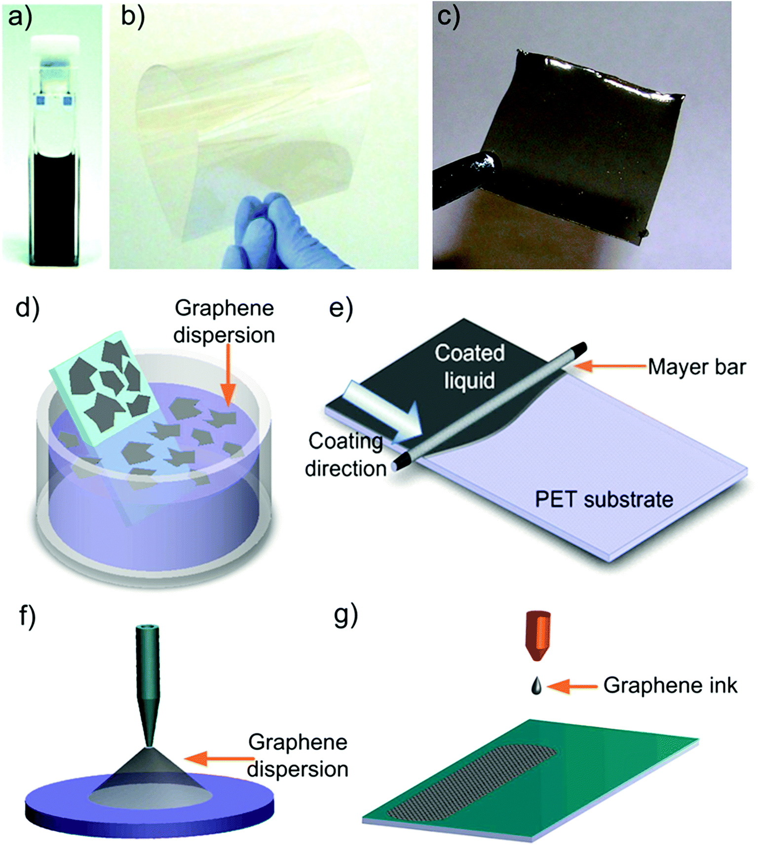 | ||
| Fig. 42 (a) Graphene ink. (b) Graphene-based TCF and (c) graphene polymer composite. (d) Dip casting, (e) rod coating, (f) spray and (g) inkjet printing of graphene inks.602 | ||
High quality graphene inks and ink-jet printed TFTs with μ ∼ 90 cm2 V−1 s−1 have been demonstrated,629 paving the way towards a fully graphene-based printable electronics.629
LPE flakes have limited size due to both the exfoliation procedure, that induces in-plane fracture, and the purification process, which separates large un-exfoliated flakes. To date, LPE-SLGs have area mostly below 1 μm2 (ref. 35, 250, 624–626, 629, 641).
LPE can also be optimized to produce GNRs, with widths <10 nm.303Ref. 303 ultrasonicated expanded graphite664 in a 1,2-dichloroethane solution of poly(m-phenylenevinylene-co-2,5-dioctoxy-p-phenylenevinylene), and ultracentrifuged, resulting in flakes and GNRs of different shapes. However, the GNR production mechanism via LPE is not well understood. Thus, more work is needed to improve it.
The goal is now to further develop LPE to get control on-demand of N, flake thickness and lateral size, as well as rheological (i.e., density, viscosity, and surface tension) properties of the resulting dispersions. A combination of theory and experiments is needed to fully understand the exfoliation process in different solvents, in order to optimise the separation of flakes in centrifugal fields, so to achieve SLG and FLG with well-defined morphological properties at a high rate.
A very desirable step is the development of techniques capable of manipulating individual flakes. Optical tweezers (OT) can trap, manipulate, control and assemble dielectric particles, single atoms, cells and nanostructures.250,665–669 These can be used to trap graphene layers and/or GNRs in liquid environments. The coupling of OT with a Raman spectrometer (Raman Tweezers250), can test solutions composition and sort N in optofluidic channels. The assessment of exfoliation yield is essential to allow further improvements. Detailed structural characterisation of the exfoliated sheets can be done by aberration-corrected HRTEM and STEM, electron energy loss spectroscopy (EELS) and in situ TEM. These can characterise the exfoliated materials down to the atomic level. The effect of structural defects on the electrical properties can also be investigated in situ.
Ref. 670 reported a scalable method, based on shear mixing of graphite, Fig. 43. During rotation, the shear mixer acts as a pump, pulling both liquid and solids into the mixing head where centrifugal forces drive them towards the edge of the rotor/stator (see Fig. 43b).670 This is accompanied by intense (power density of ∼100 W l−1) shear as the materials are driven between the rotor and screen and then out through the perforations in the stator and into the main volume of the liquid. This method can produce ∼1.4 g h−1 of mostly FLG with YW = 3.35% and could be applied to other LMs.670
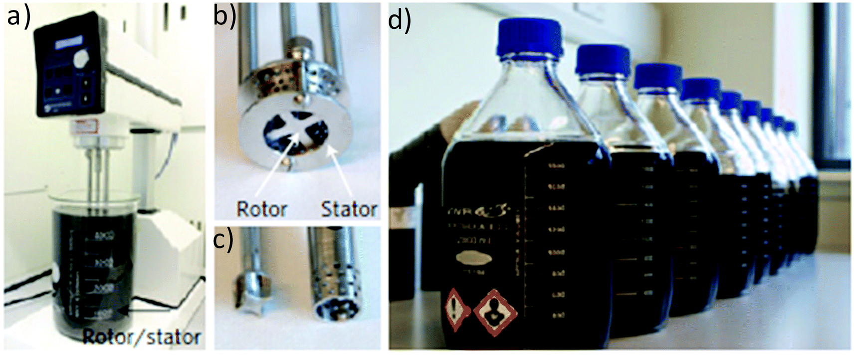 | ||
| Fig. 43 (a) Silverson model L5M high-shear mixer with mixing head in a 5 liters beaker of dispersion containing graphitic flakes. Close-up view of (b) mixing head (diameter = 32 mm) and (c) mixing head (diameter = 16 mm) with rotor (left) separated from stator. (d), bottles containing the final dispersions. Adapted from ref. 670. | ||
4.1.2.2. LPE of graphite oxide. LPE is a versatile technique and can be exploited not only for the exfoliation of pristine graphite, as reported in section 4.1.2.1, but also for the exfoliation of graphite oxide and graphite intercalated compounds (GICs), which have different properties with respect to pristine graphite,602 as discussed in this and the next section.
The oxidation of graphite in the presence of potassium chlorate (KClO3) and fuming nitric acid was developed by Brodie in 1859 while investigating the reactivity of graphite flakes.671 This process involved successive oxidative treatments of graphite in different reactors.671 In 1898, Staudenmaier modified Brodie's process by using concentrated sulphuric acid and adding KClO3 in successive steps during the reaction.672 This allowed carrying out the reaction in a single vessel, streamlining the production process.673 However, both methods were time consuming and hazardous, as they also yielded chlorine dioxide (ClO2) gas,104 which can explosively decompose into oxygen and chlorine.674 Graphite oxide (GrO) flakes were already investigated by Kohlschtter and Haenni in 1918,675 and the first TEM images reported in 1948 by Ruess and Vogt676 showed the presence of single sheets of GO.
In 1958, Hummers modified the process using a mixture of sulphuric acid, sodium nitrate and potassium permanganate.677 Avoiding KClO3 made the process safer and quicker with no explosive byproducts.677 These aggressive chemical processes disrupt the sp2-bonded network and introduce hydroxyl or epoxide groups,678–680 in the basal plane, while carbonyl and carboxylic groups, together with lactone, phenol and quinone attach to the edges (see Fig. 44). However, the introduction of these functional groups is essential for the GO production and subsequent liquid dispersion.
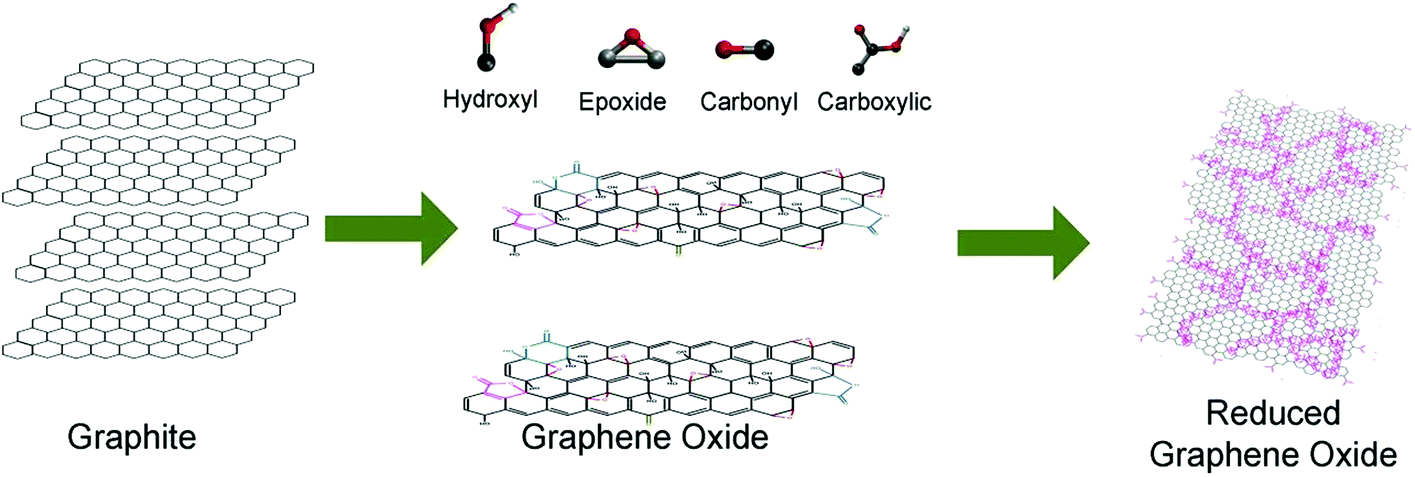 | ||
| Fig. 44 GO synthesis and reduction. Graphite can be oxidized with different procedures in the presence of strong acids. The GO flakes have the basal plane functionalized with epoxy and hydroxyl groups, both above and below it, and the edges with a variety of functional groups. This makes GO sheets defective. A partial restoration of the electronic properties is obtainable following different reduction strategies.602 | ||
GO flakes can be produced via sonication,303,681 stirring,682 thermal expansion,683etc., of GrO. The aforementioned functional groups make them strongly hydrophilic, allowing their dispersion in pure water,303,681 organic solvents,682,684 aqueous mixtures with methanol, acetone, acetonitrile685 or 1-propanol and ethylene glycol.686 However, although large GO flakes, up to several microns,687 can be produced, they are defective679 and insulating, with Rs ∼ 1012 Ω □−1(Ohm per square), or higher.688
GO is luminescent under continuous wave irradiation.689 Visible excitation gives a broad PL spectrum from visible to near-infrared,564 while blue emission690 is detected upon UV excitation. This makes GO an interesting material for lighting applications (e.g. light emitting devices691) and bio-imaging.564
Several processes have been developed to chemically “reduce” GO flakes, i.e. decrease the oxidation state of the oxygen-containing groups in order to re-establish σ and κ as close as possible to pristine graphene.602 In 1962, the reduction of GrO in alkaline dispersions was proposed for the production of thin (down to single layer) graphite lamellaes.680,692 Other methods involve treatments by hydrazine,303,693 hydrides,686,694p-phynylene,695 hydroquinone694etc., as well as dehydration696 or thermal reduction.679,684,697 UV-assisted photocatalyst reduction of GO was proposed,698 whereby GO reduces as it accepts electrons from UV irradiated TiO2 nanoparticles.698
The charge transport in RGO is believed to take place via variable-range hopping (VRH).690,699 Individual RGO sheets have been prepared with σ ∼ 350 S cm−1,700 while higher values (1314 S cm−1) were achieved in thin films,701 because in the latter RGO flakes are equivalent to resistors in parallel.693 These σ are much bigger than those of organic semiconductors (e.g. poly(β′-dodecyloxy(-α,α′-α′,α′′)terthienyl) (poly(DOT)) ∼ 10−3 S cm−1 for charge carriers, n ∼ 1021).702
It is important to differentiate between dispersion-processed flakes, retaining the graphene electronic properties, such as those reported in ref. 35, 250, 624–627, 629, and GO flakes, such as those in ref. 303, 681–684.
GO and RGO can be deposited on different substrates with the same techniques used for LPE graphene, discussed in section 4.1.2.1, 11.1. GO and RGO are ideal for composites,703 due the presence of functional groups, which can link polymers.703
Ref. 704 reported RGO sheets with σ ∼ 103 S m−1, high flexibility, and surface areas comparable to SLG, thus interesting for a range of electronic and optoelectronic applications. Thin films of RGO have been tested as FETs,705 transparent conducting films (TCFs),706 electro-active layers,707–709 solar cells,710 ultrafast lasers,711,712etc. Patterning has been used to create conductive RGO-based electrodes.690
Heating-driven reduction has the potential to produce good quality graphene structures. Laser heating in an oxygen-free environment (Ar or N2) can be done with a spatial resolution down to a few μm and T up to 1000 °C. This may enable graphene micro-patterns fabrication. This methodology could pave the way to large-scale production of patterned graphene.
Other strategies to create reactive dangling bonds directly on edges or GNRs have been developed.708 Thus, GO and CMG are also attractive for bio/medial applications, for the development of new biosensors, for bio-labelling and bio-imaging,564 for tissue engineering, for drug delivery and as antibacterial.
Another option is to induce magnetism by chemical functionalization. Theoretical studies predicted that defective graphene could be semiconducting and magnetic.713–715Ref. 716 reported a mixture of disordered magnetism regions (ferro, super-paramagnetic and antiferromagnetic) on graphene using nitrophenyl functionalization. The aim is to induce long-range ferromagnetic order by controlling the chemisorbed sites for spintronics.716
Functionalized graphene (FG) could be used as substrate for the deposition and organization of supramolecular layers and (or) enhance the local reactivity by inducing a curvature. Molecules are used either for doping,717,718 or can exploit graphene itself as substrate for the self-organization of supramolecular layers,719,720 and (or) Moiré patterns, e.g. in the case of graphene/Ru(0001).721,722
The outstanding issue is to understand the electronic interaction between molecules and graphene and the balance between molecule–molecule and molecule–substrate interaction for the realization of supramolecular networks.
A demonstration of the possibility to functionalize graphene with individual molecules is the molecular spin valve device reported in ref. 723, made by decorating a graphene nanoconstruction with TbPc2 magnetic molecules.723 These experiments open a wide research field and several intriguing questions on spintronics.
4.1.2.3. LPE of intercalated graphite. GICs are formed by periodic insertion of atomic or molecular species (intercalants) between graphene layers.724,725 GICs are typically characterized in terms of a ‘staging’ index m, i.e. the N between two adjacent intercalant layers. Thus, e.g., a stage 3 GIC (see Fig. 45) has each 3 adjacent graphene layers sandwiched by 2 intercalant layers726 (the latter can also be more than 1 atom thick).
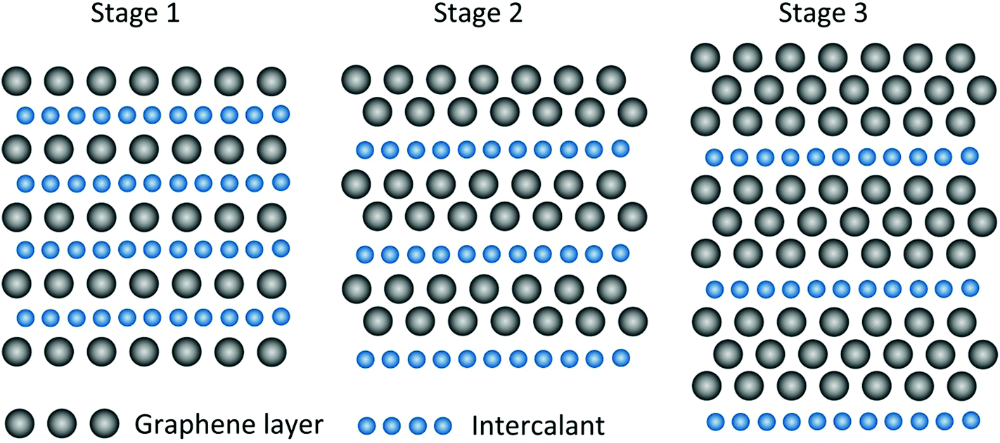 | ||
| Fig. 45 Graphite intercalation compounds. In stage 1, SLG alternate with intercalant layers. In stage 2, stage 3, etc., 2, 3, etc. graphene layers separate two intercalant layers. Adapted from ref. 602. | ||
GICs have a long history since the first recorded production by Schafhaeutl in 1840.724Ref. 726, 727 summarized the historical development of GICs. The first determination of stage index by X-ray diffraction was done in 1931 by Hoffman and Fenzel.728 Systematic studies started in the late 1970s.
Intercalation of atoms or molecules with different m gives rise to a wide variety of electrical,726 thermal726 and magnetic properties.726 GICs have potential as highly conductive materials.726,729–731 GICs with metal chloride or pentafluoride intercalants, such as antimony pentafluoride (SbF5) and Arsenic pentafluoride (AsF5), received much interest since the 1970s.726,729–731E.g., AsF5-GICs has slightly higher σ (6.3 × 10⁵ S cm−1)729 than bulk Cu730,731 (5.9 × 10⁵ S cm−1),729 while the graphite in plane σ is ∼4.5 × 10⁴ S cm−1.732 The σ increase is assigned to injection of carriers from the intercalate layer, with low μ, to the graphite layers, with high μ.726
GICs can be superconducting733 with transition temperatures up to 11.5 K for CaC6 GICs at ambient pressure,734 and higher with increasing pressure.735 Moreover, GICs are also promising for hydrogen storage, due to a larger interlayer spacing.736 GICs are already commercialized in batteries,737 in particular, in Li-ion batteries since the 1970s.738–740 GICs have also been used as negative electrodes (anode during discharge) in Li-ion batteries with the introduction of solid electrolytes.741,742
The most common production strategies include two-zone vapour transport726,743,744 exploiting T differences between graphite and intercalants745 and, sometimes, the presence of gases,745e.g. Cl2 for intercalation of AlCl3.726 GICs can be produced in single (for binary or ternary GICs) or multiple steps, the latter when direct intercalation is not possible.746 Hundreds of GICs with donor (alkali, alkali earth metals, lanthanides, metal alloys or ternary compounds, etc.) or acceptor intercalants (i.e. halogens, halogen mixtures, metal chlorides, acidic oxides, etc.) have been reported.726,744
The intercalation process increases the graphite interlayer spacing, especially for low stage index GICs,747,748E.g., K, Rb or Cs-GICs have interlayer distance ∼0.53–0.59 nm, while larger intercalants, such as dimethylsulfoxide, give an interlayer distance ∼0.9 nm,748i.e. 1.5 to ∼3 times larger than the ∼0.34 nm spacing in pristine graphite. This makes GICs promising to produce graphene via LPE, even without ultrasonication.628,747–750 However, although the exfoliation process is often called spontaneous,628,750 due to the absence of ultrasonication, it requires mechanical energy, often provided by stirring.628,750 To date it is possible to exfoliate GICs with lateral sizes ∼20 μm with YM ∼ 90%,749 and μ ∼ tens cm2 V−1 s−1.749
Note that many GICs tend to oxidize in air,726,751 and require a controlled ambient for their processing.726,751 This, coupled with the additional steps for GIC production, is one of the primary reasons why GICs are not yet extensively used to produce graphene via LPE. However, ref. 752 recently reported FeCl3 intercalated FLGs air-stable for up to one year.
Aspects of the intercalation mechanism, key for applications, still need to be clarified. This has implications for life duration of Li-ion batteries.753–755 The role of the solvent and the search for novel strategies for intercalation are also crucial, particularly to achieve large quantities of LPE graphene. Some GICs were shown to be spontaneously soluble in polar solvents without need of sonication or high shear mixing.628,750
Other open questions are: what is the role of the intercalant, the charge transfer to the graphene layer and the modification of the graphene band structure.
4.2. Growth on SiC
The production of graphite from SiC, Fig. 39e, was reported by Acheson as early as 1896 (ref. 59) for lubricant applications.59 The growth mechanism has been investigated since the 1960s.760 Both polar surfaces, the Si-terminated (0001) and the C-terminated (000![[1 with combining macron]](https://www.rsc.org/images/entities/char_0031_0304.gif) ) surface, annealed at high T under UHV tend to graphitize, because of Si evaporation.756,757Ref. 758–760 reported the production of graphene films by thermal decomposition of SiC above 1000 °C. This is not a self-limiting process and areas of different film thicknesses may exist.759
) surface, annealed at high T under UHV tend to graphitize, because of Si evaporation.756,757Ref. 758–760 reported the production of graphene films by thermal decomposition of SiC above 1000 °C. This is not a self-limiting process and areas of different film thicknesses may exist.759
On the (0001)-surface (see Fig. 46) the graphene layer is grown on top of a C-rich (6√3 × 6√3)R30° reconstruction with respect to the SiC surface, called the buffer layer.761 This consists of C atoms arranged in a graphene-like honeycomb structure,761 but without graphene-like electronic properties, because ∼30% are covalently bonded to Si.761
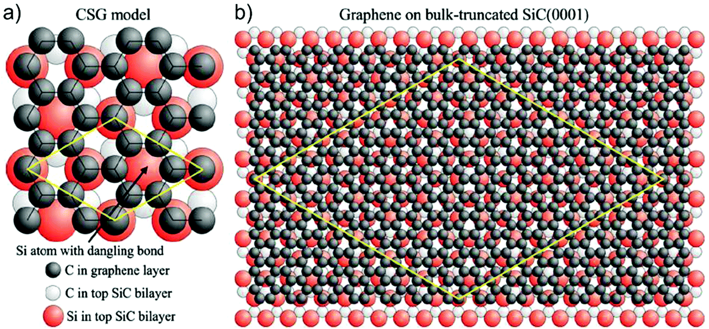 | ||
| Fig. 46 (a) Top view of covalently bound stretched graphene (CSG) model on SiC(0001). (b) graphene on bulk-truncated SiC(0001) surface, Adapted from ref. 761. | ||
The buffer layer can be decoupled from the Si(0001)-face by hydrogen intercalation,763 becoming a quasi-free-standing SLG with typical linear π bands.763 In contrast, the interaction between graphene and the C(000)-terminated face is much weaker.761
Growth of graphene on SiC is usually referred to as “epitaxial growth”,764 even though there is a large lattice mismatch between SiC (3.073 Å) and graphene (2.46 Å) and the carbon rearranges itself in a hexagonal structure as Si evaporates from the SiC substrate, rather than being deposited on the SiC surface, as would happen in a traditional epitaxial growth process. The term “epitaxy” derives from Greek, the prefix epi means “over” or “upon” and taxis means “order” or “arrangement”. In 1928 Royer765 used the term “epitaxy” referring to the “oriented growth of one substance on the crystal surface of a foreign substance”. If the growing crystal and the substrate have the same lattice constants these are lattice matched.766 The use of “epitaxial” as the adjectival form of epitaxy has been subjected to some criticism already in the sixties, because it is incorrect from the philological point of view.767 Epitactic is the correct form.767 In 1965 epitaxic was recommended by ref. 768. However, the word “epitaxial” is now widely used and any attempt to change it is unrealistic.602 We will thus use “epitaxial” as adjectival form of epitaxy. There are two general epitaxial growth processes depending on the substrate, homo- and hetero-epitaxy. In the case of homoepitaxy the substrate is of the same composition and structure as the growing film, whereas in the case of heteroepitaxy the substrate is of a different composition and may not be perfectly lattice matched.602
It would be desirable to grow graphene on a lattice matched isostructural substrate in order to minimize defects, like misfit dislocations, as in the case of traditional semiconductors.769 However, with the exception of graphite, where the growth would be referred to as homoepitaxy, and would not be very useful for obvious reasons, there are few substrates that are isostructural and nearly lattice matched to graphene. There are two potential substrates that might meet the aforementioned requirement, h-BN and hexagonal closed packed (hcp) Co.602 H-BN has the lowest lattice mismatch ∼1.7%. Cobalt metal (hcp at T < 400 °C) also has a small lattice mismatch ∼2%.602 There are other hcp metals like Ru, Hf, Ti, Zr, but these have much larger lattice mismatch770 than that between Co and graphene, and there are face centre cubic metals like Ni, Cu, Pd, Rh, Ag, Au, Pt and Ir that have a range of lattice mismatch on the (111) planes.602 Therefore, from an epitaxial growth perspective, it would be desirable to grow on oriented single crystal Co (see section 4.3, 4.4) as performed by ref. 771. Growth on Co would also require transfer to other non-metallic substrates, discussed later. SiC substrates could be a natural substrate were if not for the fact that the lattice mismatch between graphene and SiC is also very large, ∼25% for both 4H-SiC (Si-face) and 6H-SiC (C-face). There have been reports of growth of LMs on highly non-lattice-matched substrates as buffer layers, due to their weak bonding to the underlying substrates,772–774 In this case, the films grow parallel to the substrate because of the anisotropic nature of their chemical bonds. Growth of graphene on SiC might be described in a similar manner.772–774
The growth rate of graphene on SiC depends on the specific polar SiC crystal face.775,776 Graphene forms much faster on the C-face than on the Si-face.775,776 On the C-face, larger domains (∼200 nm) of multilayered, rotationally disordered graphene are produced.777,778 On the Si-face, UHV annealing leads to small domains, ∼30–100 nm.778 The small-grain structure is attributed to morphological changes of the surface in the course of high-T UHV annealing.759 Indeed, ref. 779, via energy-resolved maps of the local density of states of graphene grown on Si-face, revealed modulations on two different length scales, reflecting both intra-valley and inter-valley scattering due to in-plane atomic defects. These defects in UHV annealed SiC are related to the relatively low growth T and the high graphitization rates in the out of equilibrium UHV Si sublimation process.775
Different strategies were proposed to control the Si sublimation rate. Ref. 780 used Si in a vapour phase establishing thermodynamic equilibrium between the SiC sample and the external Si vapour pressure to vary the T of the phase transition from the Si-rich (3 × 3) to the C-rich (6√3 × 6√3)R30° structure, the buffer layer, and the final graphene layer. The resulting domains were an order of magnitude larger than those grown under UHV.762
Ref. 759 used the “light bulb method” to grow graphene, exploiting a 80-year old process first developed to extend the lifetime of incandescent light bulb filaments.781 This uses Ar in a furnace at near ambient pressure (1 bar) to reduce the Si sublimation rate.759 Indeed, in Ar no sublimation was observed until 1500 °C,759 whereas Si desorption started at 1150 °C in UHV,759 thus enhancing surface diffusion, with complete surface restructuring before graphene formation.759 The resulting films on the Si-face have ∼50 μm domains,759 almost 3 orders of magnitude larger than in UHV annealing.777,778
Si sublimation can also be controlled by confining SiC in a graphite enclosure (either in vacuum775 or in an inert gas775) limiting the Si escape, maintaining a high Si vapour pressure. This keeps the process close to thermodynamic equilibrium, producing either SLG775 or FLG775 films over large (cm scale) areas, both on Si- and C-face. High T annealing can also give GNRs and GQDs.782,783
To date, graphene grown on the Si-face has a RT μ up to ∼500–2000 cm2 V−1 s−1 (ref. 775), with higher values on the C-face (∼10000–30000 cm2 V−1 s−1).775–777 For near-intrinsic samples (8.5 × 1010 cm−2)784 RT mobilities up to ∼150000 cm2 V−1 s−1 on C-face785 and ∼5800 cm2 V−1 s−1 on Si-face785 were reported. Ref. 100 reported an exceptionally high μ in a 40-nanometre-wide GNR grown on the (0001) face of SiC. These GNRs have shown ballistic conductance (at 4 K) on a length scale greater than ten micrometres with μ ∼ 6 × 106 cm2 V−1 s−1.100 This is equivalent to Rs ∼ 1 Ω □−1 (ref. 100).
Graphene on SiC has the benefit that SiC is an established substrate for power electronics.786 Top gated transistors have been fabricated from graphene on SiC on a wafer scale.787 High frequency transistors have also been demonstrated with 100 GHz cut-off frequency788 higher than state-of-the-art Si transistors of the same gate length.433 Graphene on SiC has been developed as a resistance standard based on QHE.146,148,151
A drawback for this technology for large scale production is the SiC wafers cost (∼$150–250 for 2′′ wafer789 at 2011 prices, compared to ∼$5–10 for same size Si wafers) and their smaller size (usually no larger than 4′′) compared to Si wafers. One approach to reduce substrate costs is to grow thin SiC layers on sapphire, the latter costing less than ∼$10 for 2′′ wafer,790 and subsequently perform thermal decomposition to yield FLG.791 Thus far, FLGs produced in this way have inferior structural and electronic quality compared to bulk SiC. Another approach is to grow SiC on Si.792 However SiC on Si is usually cubic,793–795 making it challenging to achieve continuous high quality graphene, due to bowing and film cracking as a consequence of high residual stress.219,220,796,797Ref. 798 grew SLG on 3C–SiC(111) with domains ∼100 μm2, combining atmospheric pressure growth759 with hydrogen intercalation,763 demonstrating that large domains can grow on 3C–SiC(111).
Future challenges are the control on the layer thickness homogeneity (currently not 100% monolayer)602 probably via better control of unintentional mis-cut angles, understanding and control of unintentional doping caused by the substrate, together with a better understanding of the effect of structural in-homogeneities (e.g. steps, wrinkles, BLG inclusions) on transport, and the mechanisms limiting μ. Other targets are the growth of graphene on pre-patterned SiC substrates, and a better control of growth on the SiC C-face, so to have SLG also on this face. The aim is also to tune the properties of graphene grown on SiC via interface engineering (e.g. SiC surface hydrogenation, etc.) and better understanding of defects generated during growth and/or interface manipulation and identification of methods to heal them. Doping of graphene by insertion of heteroatoms needs also to be addressed, with the aim to have control on the procedures and consequently on the properties of the graphene flakes. The achievement of many of the aforementioned goals will require a careful investigation and improvement of the substrates. A critical point to be addressed is the transfer of SLG directly from a SiC surface to a target substrate, where the difficulty arises from the strong binding of graphene to the SiC surface.761,775,776 This issue was addressed by ref. 799 that developed a method in which a film consisting of SLG or BLG grown on SiC is exfoliated via the stress induced with a Ni film and transferred to another substrate. Other points to be addressed are routes to improve growth of cubic SiC as substrate, and the growth of insulating SiC layers on cheap on-axis n-type substrates, in order to replace expensive semi-insulating substrate materials.
The graphene quality and N are strongly dependent on the growth and annealing conditions. The advantage over standard CVD is the graphene quality control achievable via tuning of carbon source thickness and annealing conditions. In addition, all the process steps occur in fully semiconductor compatible environment. Thus, industry can then take benefit of the versatility of this method to integrate graphene in their process flow. The long term goal is a totally controlled graphene nano-structuring, so to produce GNRs and GQDs on demand. This is motivated by the prospect of band gap creation in graphene.
4.3. Growth on metals by precipitation
Carbon can be deposited on a metal surface by a number of techniques, e.g.: flash evaporation, physical vapour deposition (PVD), CVD, and spin coating. The carbon source can be a solid,800,801 liquid,802,892,803 or gas.849 In the case of a pure carbon source, flash evaporation804 or PVD805 can be used to deposit carbon directly on the substrate of interest, if non-carbide forming but with a finite carbon solubility, before before diffusion at high T followed by precipitation of graphite (graphene) upon cooling. When the solid source is a polymer, it can be spun on the metal substrate at RT, followed by high T annealing and growth.801Segregation from carbon-containing metal and inorganic substrates is another approach to graphene growth,806–808 see Fig. 39f. The first reports of synthetic growth of graphite, i.e. not extracted from mined natural sources, on transition metals date back to the early 1940s.806–808 It was not until the 1970s, however, when the details of the growth process were elucidated. Ref. 809 identified, via a combination of Auger and low-energy electron diffraction (LEED), SLG formed from carbon precipitation, following high T annealing of Co, Pt, or Ni. This process exploits the T-dependent solubility of interstitial carbons in transition metals (i.e. Ni(111),810 Ru(001),811 Ir(111),812 Pt(111),813 Pd(100),813etc.) or inorganic chemical compounds (i.e. LaB6814 ) to achieve layer-by-layer growth of graphene on the surface. The amount of carbon that can be dissolved in most metals is up to a few atomic%.815
Materials for substrates are selected among those which do not form carbides, in order to eliminate the competition between forming a carbide and graphite/graphene growth. Elements like Ti, Ta, Hf, Zr and Si, etc. form thermally stable carbides, as shown by the phase diagram,816–820 thus are not “ideal” substrates for graphite/graphene growth. Moreover, all these have a large (>20%) lattice mismatch with graphene. The transition metal is first annealed to high T (>1000 °C) in UHV, where the bulk solubility of interstitial carbon is high, then cooled to decrease solubility, resulting in its segregation as a graphene film.821
Graphite can also be obtained from carbon saturated molten iron during the formation of steel.822 In accordance to the process just described, Fe is supersaturated with carbon, and the excess carbon precipitates.822 This is usually referred to as “Kish graphite”,823 derived from the German “Kies”, used by steel workers to refer to the “mixture of graphite and slag separated from and floating on the surface of molten pig iron or cast iron as it cools”.227
Significant attention has been devoted to the use of inexpensive metals such as Ni,824–826 and Co.827 Growth on noble metals such as Ir,812 Pt,813 Ru,811 and Pd,813 aimed at a better understanding of the growth mechanisms and/or at obtaining samples suitable for fundamental studies, e.g. for STM,828 that require a conductive substrate. It would be desirable in any case to have a stable metal that can promote graphene single crystal growth, and the use of (111) oriented Ni or Co could help in this sense, since they facilitate the hexagonal arrangement of carbon atoms.
The monolayer-graphite/graphite growth process on Ni was first investigated in 1974 in ref. 809. SLG on Ni(111) was observed at T > 1000 K by Auger analysis, followed by graphite formation upon cooling. During high T annealing, carbon diffuses into the metal until it reaches the solubility limit. Upon cooling, carbon precipitates forming first graphene, then graphite.809 The graphite film thickness depends on the metal, the solubility of carbon in that metal, the T at which the carbon is introduced, the thickness of the metal and the cooling rate.
To get large metal grains with crystalline orientation i.e. Ni(111),829 an annealing of the metal surface is often performed. Carbon segregation in Ni(111) was investigated in ref. 830, 831 with control of number of surface C atoms by adjusting the annealing T.831
The graphene–metal distance and its nano-rippling on the metallic substrate determine the so-called graphene–metal Moiré superstructure.812,832 The latter is due to a mismatch between substrate and graphene lattice, and depends on the metal substrate. For lattice mismatches between graphene and substrate below 1%, commensurate superstructures, where the resulting broken symmetry is a doubling of the unit cell along one axis (i.e. 1/2, 0, 0), are formed.833 This is the case for Ni(111)821 and Co(0001).834 On the other hand, larger mismatches yield incommensurate (total loss of symmetry in a particular direction, i.e. (0.528,0,0)) moiré superstructures, such as in Pt(111),835 Ir(111),836 or Ru(0001)832,837 Indeed, graphene grown on Ir(111) yields flakes of well-defined orientation with respect to the substrate.812 On the contrary, graphene obtained via high-T segregation of C on Ru(0001) has a spread of orientations.837 Moreover, the graphene/Ru lattice mismatch results in a distribution of tensile and compressive strains.838 This causes corrugation, due to buckling, and the formation of ∼1.7 Å humps.838 The Moiré superstructure could be eliminated by the adsorption of oxygen on the metal surface acting as intercalant.839
Growth of graphene by precipitation requires careful control of the metal thickness, T, annealing time, cooling rate, and metal microstructure. Ref. 840 reported growth on Ni, Co and Ru on sapphire. Through the suppression of grain boundaries, ref. 840 demonstrated uniform growth on Ru by a surface catalyzed reaction of hydrocarbons, but not on Ni and Co.840 Both SLG and FLG were observed on Ni and Co, presumably due to the higher solubility of carbon and incorporation kinetics in comparison to Ru at the same T.840 However, ref. 771 grew graphene on epitaxial Co on sapphire, achieving SLGs, in contrast to FLGs in ref. 840. An alternative strategy for SLG growth on high C solubility substrates was proposed by ref. 841 using a binary alloy (Ni–Mo). The Mo component of the alloy traps all the dissolved excess C atoms, forming molybdenum carbides and suppressing C precipitation.841 Graphene was also grown on Ru(0001) on sapphire.842
One of the shortcomings of the growth on metals is that most applications require graphene on an insulating substrate. Ref. 843 suggested that graphene can be grown directly on SiO2 by the precipitation of carbon from a Ni film deposited on the dielectric surface. This process has favourable perspectives but needs further refinement.
The aim of the work on graphene produced by carbon segregation is eventually to achieve a full control on graphene quality and N. These are strongly dependent on the growth and annealing conditions and a full control on the latter is still missing. Deeply connected with this first issue are the requirements to obtain high quality graphene, where defects such as grain boundaries, pentagon–heptagon pairs, point defects,844 wrinkles,845 or local deformations are avoided or minimized. A further open issue is the transfer of graphene produced via carbon segregation onto arbitrary substrates and a process optimized for the various graphene applications still requires significant effort.
4.4. Chemical vapour deposition
Chemical vapour deposition is a process widely used to deposit or grow thin films, crystalline or amorphous, from solid, liquid or gaseous precursors of many materials. CVD has been the workhorse for depositing materials used in semiconductor devices for decades.846The type of precursor is usually dictated by what is available, what yields the desired film, and what is cost-effective for the specific application. There are many different types of CVD processes: thermal, plasma enhanced (PECVD), cold wall, hot wall, reactive, and many more. Again, the type depends on the available precursors, the material quality, the thickness, and the structure needed; cost is also an essential part of selecting a specific process.
The main difference in the CVD equipment for the different precursor types is the gas delivery system.847 In the case of solid precursors, the solid can be either vaporized and then transported to the deposition chamber,847 or dissolved using an appropriate solvent,847 delivered to a vaporizer,847 and then transported to the deposition chamber.847 The transport of the precursor can also be aided by a carrier gas.847 Depending on the desired deposition temperature, precursor reactivity, or desired growth rate, it may be necessary to introduce an external energy source to aid precursor decomposition.
One of the most common and inexpensive production methods is PECVD. The creation of plasma of the reacting gaseous precursors allows deposition at lower T with respect to thermal CVD. However, since plasma can damage the growing material, one needs to design the equipment and select process regimes that minimize this damage. The details of the growth process are usually complex, and in many cases not all of the reactions are well understood. There are many different ways to perform plasma assisted CVD (see ref. 848 for an overview). It is however important to match the equipment design with the material one is trying to deposit and the precursor chemistry. Graphene should be simpler than multi-component systems, since it is a single element material. As with many other materials, graphene growth can be performed using a wide variety of precursors, liquids, gases, solids, growth chamber designs, thermal-CVD or PECVD, over a wide range of chamber pressures and substrate T.
In 1984 Kholin et al.852 grew graphene by CVD on Ir, to study the catalytic and thermionic properties of Ir in the presence of carbon.853 Since then, other groups exposed metals, such as single crystal Ir833,854 to carbon precursors and studied the formation of graphitic films in UHV systems.
The first studies of graphene growth on metals were primarily focused on the understanding of the catalytic and thermionic activities of the metal surfaces in the presence of carbon.855 After 2004, the focus shifted to the actual growth of graphene. Low pressure chemical vapour deposition (LPCVD) on Ir(111) using an ethylene precursor was found to yield graphene structurally coherent even over the Ir step edges.833 While Ir can certainly be used to grow graphene by CVD because of its low carbon solubility,815 it is difficult to transfer graphene to other substrates because of its chemical inertness. Ir is also expensive. Growth on Ni856 and Co827,857, metals compatible with Si processing since they have been used for silicides for over two decades,858–862 and less expensive than Ir, poses a different challenge, i.e. FLGs are usually formed,825–827,849,854 and SLGs are non-uniform. Therefore, while many papers claim CVD growth at high T on Ni and Co,825–827,849,854 the process is in fact carbon precipitation, not yielding uniform SLG, but rather FLG films. The shortcoming of high solubility or expensive and chemically unreactive metals motivated the search for a process and substrate that would be better suited to yield SLG.
The first CVD growth of uniform, large area (∼cm2) graphene on a metal surface was reported in 2009 by ref. 6 on polycrystalline Cu foils, exploiting thermal catalytic decomposition of methane and low carbon solubility. This process is almost self-limited, i.e. growth mostly ceases as soon as the Cu surface is fully covered with graphene, save ∼5% of the area, consisting of BLG and 3LG.6,863 Large area graphene growth was enabled principally by the low C solubility in Cu,864 and Cu mild catalytic activity.865
Growth of graphene on Cu by LPCVD was then scaled up in 2010 by ref. 7, increasing the Cu foil size (30 inches), producing films with μ ∼ 7350 cm2 V−1 s−1 at 6 K. Large grain, ∼20–500 μm, graphene on Cu with μ ranging from ∼16400 to ∼25000 cm2 V−1 s−1 at RT after transfer to SiO2 was reported in ref. 866 and from ∼27000 to ∼45000 cm2 V−1 s−1 on h-BN at 1.6 K in ref. 867. There is now a huge effort towards the optimization and the growth of high quality single crystal graphene by LPCVD. Ref. 868 synthesized large (∼4.5 mm2) single crystal hexagonal SLG domains on commercial polycrystalline Cu foils, indicating the potential for large scale at low cost. The as synthesized graphene had μ ∼11000 cm2 V−1 s−1 on a SiO2/Si substrate at RT. Ref. 869 by controlling surface oxygen, has repeatably grown centimeter-scale single-crystal graphene domains. The μ measured for these single-crystal graphene samples ranged from ∼40000 to ∼65000 cm2 V−1 s−1 at 1.7 K and from ∼15000 to ∼30000 cm2 V−1 s−1 at RT. Since it is not possible to measure the films while still on Cu, it is difficult to determine if there is degradation as a result of transfer.
The current understanding of the growth mechanism is as follows: carbon atoms, after decomposition from hydrocarbons, nucleate on Cu, and the nuclei grow into large domains.866,870 The nuclei density is principally a function of T and pressure and, at low pressure, mTorr, and T > 1000 °C, very large single crystal domains, up to ∼1 cm869 are observed. However, when the Cu surface is fully covered, the films become polycrystalline, since the nuclei are not registered,6,865,868,870i.e. they are mis-oriented or incommensurate with respect to each other, even on the same Cu grain. This could be ascribed to the low Cu–C binding energy.871 It would be desirable to have substrates with higher binding energy with C.871 However, while Ru is compatible with Si processing,872 oriented Ru films may be difficult to grow on large (300–450 mm) Si wafers, or transferred from other substrates.
Graphene nucleation needs to be investigated, to control and enhance domain size, via controlled and multi-step exposures. Basic reaction kinetics and layer-by-layer growth need to be investigated by dedicated surface science experiments. Real-time spectroscopy could in principle be of great help to monitor CVD-graphene growth and understand thickness distribution as well as optimize the growth conditions. Cu pre-treatments, electrochemical polishing,873,874 and high-pressure annealing868 are shown to be critical for suppressing graphene nucleation site density. Electrochemical polishing873,874 cleans the Cu surface and removes the impurity layer.
There are some difficult issues to deal with when growing graphene on most metal substrates, especially Cu, because of the difference in thermal expansion coefficient between Cu and graphene, of about an order of magnitude.875 The thermal mismatch gives rise to a significant wrinkle density upon cooling.863 These wrinkles are defective, as determined by Raman spectroscopy,866 and may also cause significant device degradation through defect scattering, similar to the effect of grain boundaries on μ in semiconducting materials.866 These defects however, may not be detrimental for many non-electrically-active applications, such as transparent electrodes. Perhaps one could use relatively cheaper substrates such as Cu (Cu is cheaper than Ir, Ru, Pt) and use an electrochemical process to remove graphene while reusing Cu, so that the cost is amortized over many growth runs. Because of some unattractive properties (e.g. surface roughening and sublimation) of Cu at the current thermal CVD growth T > 1000 °C, the community has been searching for new substrates that take advantage of the self-limited growth process, in addition to dielectrics. Ref. 876 reported growth of SLG on Ni(111) at lower T, 500–600 °C, using ethylene by UHV CVD, and identified the process as self-limiting, presumably due to the low C solubility in Ni at T < 650 °C.877 However, the T range within which graphene can be grown on Ni is narrow, 100 °C,876 and could result in a Ni2C phase,876 which can give rise to defects in the Ni crystal. Thus one could surmise that any graphene could be non-uniform across the Ni–Ni2C regions.
Graphene was also grown on Cu by exposing it to liquids or solid hydrocarbons.801,878Ref. 878 reported growth using benzene in the T range 300–500 °C.
The presence of the substrate generally modifies the graphene electronic properties, thus it is of paramount importance to optimize the interaction between graphene and substrate. This can be tuned by applying surface treatments that, in turn, can provide additional control on the graphene properties. E.g., substrates and interfacial dielectrics with optimized properties would enable high μ devices.
The process space for SLG-CVD growth is very wide and depends on many factors, from substrate choice, to specific growth conditions, as well as variables not under direct control. It is critical to know the material requirements for specific applications, so that one can tune the growth process/conditions to the application. Growth of graphene on single crystal substrates would be a desired route for improving electronic properties. Following the growth of graphene on Cu, ref. 879 developed a Co deposition process to form highly crystalline Co on c-plane sapphire where they grew SLG by CVD at high T. However, they did not distinguish between face centred cubic (fcc)(111)Co and hcp(0002)Co and did not comment on potential phase transformation issues at T lower than the fcc to hcp phase transition (∼400 °C). While this process may seem incompatible with Si processing, and the material cost could be high, it is important to learn how to take advantage of processes that enable growth of higher quality graphene on stable surfaces, not necessarily single crystals.
Another question is: can we controllably grow FLGs? Catalytic decomposition of CO on various metals, such as Fe, Cu, Ag, Mo, Cr, Rh, and Pd, was studied by Kehrer and Leidheiser in 1954.808 They detected graphitic carbon on Fe after exposure to CO for several hours at 550 °C, but found the other metals to be inactive. The presence of BLG and TLG on Cu6 poses the question of the growth process for these isolated regions, since at first one would like to grow uniformly SLG. Growth of controlled Bernal stacked films is not easy, but small regions have been observed.880Ref. 880 reported homogenous BLG by CVD on Cu. However, it not clear whether the films are of high enough quality for high performance electronic devices, since ref. 880 did not map the D peak, and μ was ∼580 cm2 V−1 s−1 at RT.
Another approach was proposed by ref. 881 by increasing the solubility of C in Cu via a solid solution with Ni, forming the binary alloy, Cu–Ni. By controlling Ni percentage, film thickness, solution T, and cooling rate, N was controlled, enabling BLG growth.881
Graphene films with size ∼50 cm and μ > 7000 cm2 V−1 s−1 were produced on Cu and transferred via a R2R process, see Fig. 47.7 The goal is now to grow high quality samples (with crystal size >1 mm) over large areas via R2R. Low pressure thermal CVD synthesis and a direct R2R transfer using photocurable epoxy resin was used to fabricate a 100 m-long graphene transparent conductive film (GTCF) with a Rs as low as 150 Ω □−1.882
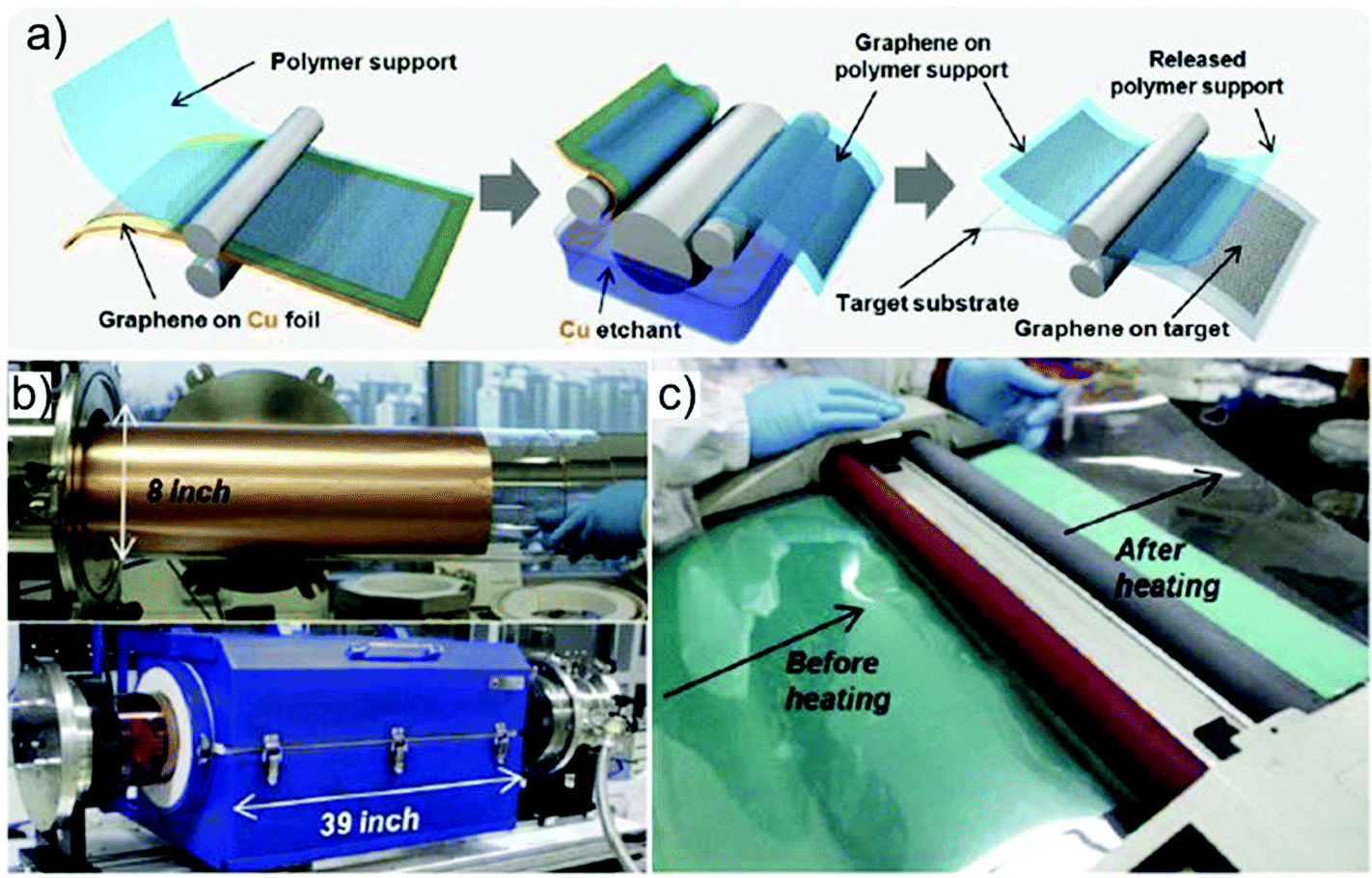 | ||
| Fig. 47 Roll-based production of graphene. (a) Schematic of the process. (b) A Cu foil is wrapped on a 7.5 inch quartz tube, then placed into an 8-inch quartz reactor. (c) R2R transfer of graphene from to a Polyethylene terephthalate (PET) film.7 | ||
Among the many areas that still need to be explored, growth on metallic alloys need yet to be investigated, the optimisation of CH4–H2–Ar mixtures has yet to be done, and the same can be said about testing and screening of alternative precursors. So far there is also little experimental insight into the underlying GB formation mechanisms, crucial to understand and control charge propagation across/within these line-defects. On one hand, there is a need for quick and easy characterization methods, able to reveal the grain structure of the CVD samples.883 On the other hand, GBs can be highly transparent,884 as well as perfectly reflective,884 and are expected to act as molecular metallic wires885 or filter the propagating charge carriers based on the valley-index.886 In order to explore and exploit these properties, the investigation of the electronic properties of individual GBs with known atomic configuration is needed. STM is a versatile tool for investigating the structure of individual GBs at atomic resolution and their electronic (and magnetic) properties on the nm scale.307
Growth of graphene on single crystal substrates is another route towards the improvement of its electronic properties, although the high cost of such substrates makes them less suitable for large-scale applications. This requires in situ growth monitoring. TEM will be fundamental to obtain atomic images of domain boundaries, as well as macroscopic images of the relative domain orientations in a film.241
Reducing the growth T is desirable in order to cut production costs, and directly integrate graphene with standard CMOS processing. Growth of FLG at 650 °C was demonstrated on Fe.887 However, the optimization of layer control and growth T below 450 °C is required for CMOS integration. Although the growth of graphene at 325 °C was shown on MgO,888 its suitability for applications is yet to be elucidated. Graphene grown on Cu foils at T as low as 300 °C using benzene as a precursor was also reported.889
MWCVD has also been proposed as a method for graphene growth.890,891Ref. 891 reported growth at 150–300° C. However, to date SLG grown has not yet been demonstrated, with the deposited films consisting of sub-micrometer flakes.891 Nevertheless, this approach was successfully used for the production of TCs.891 With further developments it could be a viable strategy for large scale, low T graphene production.891
A key target is thus the development of low T growth on large area, by understating and optimising plasma chemistry.
Low-T, high-density pulsed micro wave plasmas (electron density close to 1012 cm−3 ) are not only usable for large area growth, but also for surface processing and work-function engineering, important for chemical functionalization, and for μ control. Systems scalable to large areas should be investigated.
The production of unsupported flakes using alcohols as carbon feedstock was also demonstrated,892,893 with the potential for up-scaling. The target is to further up-scale the CVD-growth, developing a protocol for a batch reactor, producing m2-sized graphene.
The development of new routes to achieve stable doping is another key need for commercialization. Different approaches are to be investigated, either during growth, by exploiting alternative precursors (i.e. pyridine), or post-growth, via “molecular doping” by stable hydrazil- and nitroxide- radicals and metal grids.
The growth of graphene on non-flat substrates such as, e.g., Cu wires or corrugated Cu substrates instead of flat Cu films, is an area to be investigated that could open new applications both in electronics, energy and catalysis.
Another key point is the development of reliable, fast, economic and environmentally friendly transfer techniques. Methods for the recovery of the metal substrates are also needed for cost reduction and environmental issues.
CVD of carbon thin films on insulators has been known since 1971.895 However, thus far, it was optimized to give highly sp3 bonded diamond-like carbons.199 Recently this approach was developed to achieve graphitic films.896,897 Growth of high-quality graphene on insulating substrates, such as SiO2, high- dielectrics, h-BN, etc. would be ideal for electronics. There have been many attempts to grow on SiC,898 sapphire899 and Si3N4/Si,900 as well as on metal oxides such as MgO,888 and ZrO2.901 However, while graphitic regions are observed at T < 1000 °C, none of the processes yield, to date, planar SLG films covering the whole surface.899 Thus far, the best quality was achieved on sapphire899 (3000 cm2 V−1 s−1 and 10500 cm2 V−1 s−1 at RT and 2 K, respectively).
h-BN was shown to be effective as a substrate for graphene CVD,902–905 and graphene produced by this method appears comparable to that grown on transition metal catalysts833,906 with promise for hetero-epitaxial growth of heterostructures (e.g. graphene/h-BN). As well as achieving direct growth on an insulator, this approach has the additional benefit of an atomically smooth substrate, comparable with diamond-like carbon (DLC) surfaces,907 with few dangling bonds and charge traps.908 Direct growth of graphene/h-BN stacks, by both CVD and metal–organic CVD (MOCVD), is the ideal alternative to tedious successive exfoliations of rare BN single crystals (mostly one source in Japan909). CVD can also give c-BN composite layers with various topologies.910 Different B and N precursors (solid, liquid, gaseous) should be tested in a variety of environments, aiming at optimum quality and layer control, and privileging less costly and harmful ones. Wafer scale extension of BN/graphene encapsulation techniques would pave the way to transport in high-frequency electronics,788 a regime exploiting Dirac Fermion optics, with no counterpart in semiconductor electronics. Substrate tailoring may optimize these properties in a broad (and economically relevant) spectrum, from microwave to optics, including millimeter waves (THz) and IR. The aim is to produce graphene on smart substrates in a single CVD run. At present, however, only FLGs were grown by CVD on h-BN, thus improved thickness control is needed. Understanding basic growth processes is needed, with the help of both in situ and ex situ characterizations. These procedures need to be adapted to more scalable conditions.
As mentioned above, growth of single crystal graphene on dielectric surfaces is highly desirable, but to date the crystal size on dielectrics is limited to micron size.911Ref. 912 reported the growth of single crystal monolayer graphene on germanium. The authors took advantage of the low (108–1010 cm−3)913 solubility of C in Ge as in the case of C in Cu to grow single crystal graphene on hydrogen-terminated Ge(110). They observed a low wrinkle density, and assigned it to the low thermal expansion coefficient difference between graphene and Ge.912 Due to the small (∼60 meV)914 binding energy between graphene and Ge, ref. 912 were able to mechanically exfoliate graphene using an Au film carrier, minimizing the defects usually created using organic material transfer methods. This is a major advance, although nucleation and surface flatness may still require optimization.
The use of plasmas to reduce T during growth/deposition was extensively exploited in the growth of nanotubes,916–923 and amorphous carbon.200–203,924–926 In 1998 ref. 316 reported SLG with a curved structure as a byproduct of PECVD of diamond-like carbon. A number of other groups later reported growth of vertical SLG925 and FLG,919,924,926–929 by microwave PECVD on several substrates, including non-catalytic, carbide forming substrates, such as SiO2. SLGs and FLGs nucleate at the surface, but then continue to grow vertically, perhaps because of the high concentration of carbon radicals,891 thus resulting in high growth rate. This material is promising for supercapacitors or other applications, such as FE, not requiring planar films.
Graphene was grown by PECVD using methane at T as low as 500 °C,930 but the films had a significant D-band, thus with quality still not equivalent to exfoliated or thermal CVD graphene.891,930 Nevertheless, ref. 891 demonstrated that growth may be carried out at low T, and the material may be used for applications without the stringent requirements of electronics. E.g., ref. 891 used PECVD at 317 °C to make TCs with Rs ∼ 2 kΩ □−1 at Tr ∼ 78%.
PECVD might address the key issue of growth at low T, in order to prepare graphene directly on substrates compatible with applications and processing technologies listed above, e.g. direct deposition on plastic. The advantage of plasma methods with respect to thermal CVD, is the production of graphitic materials without metal catalyst over a wide range of growth conditions, both surface-bound and freestanding.917
However, large domains are needed, together with a reduction of damage caused by direct plasma during growth, that might limit the quality of graphene that can be achieved with this approach. Nevertheless, this approach seems to be promising for TCs.7
Inductively coupled plasma (ICP) CVD, (where the deposition pressure and the applied power to the plasma are controlled from two radio frequency-generators; one connected to the ICP-source, the other to the substrate931) was also used to grow graphene on 150 mm Si,931 achieving uniform films and good transport properties (i.e. μ up to ∼9000 cm2 V−1 s−1). This process is still under development with insufficient data on the structure of the material.
The long term target plan (>10 years) is to achieve on-demand graphene deposition on insulator/Si and other materials on 300–450 mm wafer size, in-line with the fabrication projections in the electronic industry. The challenge is to develop an integrated ALD-PECVD process that would allow deposition of compatible insulators at the same time as synthesising graphene. This should be done without compromising the quality of the graphene layer.
4.5. Molecular beam epitaxy growth of graphene on insulating surfaces
MBE is a UHV-based technique for producing high quality epitaxial structures with monolayer control.932 Since its introduction in the 1970s932 as a tool for growing high-purity semiconductor films, MBE has evolved into one of the most widely used techniques for epitaxial layers of metals, insulators and superconductors, both at the research and the industrial level. MBE of single crystal semiconductors, e.g. GaAs, is well-established and has produced hetero-junctions with the current record μ (3.5 × 107 cm2 V−1 s−1 (ref. 933)). MBE has also produced record low threshold current density multi-quantum-well lasers.934 MBE can achieve precise control of both the chemical composition and the doping profile. MBE can use a wide variety of dopants compared to CVD epitaxial techniques.MBE can be used to grow carbon films (see Fig. 39h) directly on Si(111),935 and is a promising approach to achieve high-purity graphene heterostructures on a variety of substrates, such as SiC, Al2O3, Mica, SiO2, Ni, etc.
MBE is more suited to grow 2–6 inch wafers rather than 30-inch ones.7 MBE graphene may find industrial applications in markets where highly specialised devices are required. Despite the conceptual simplicity, a great technological effort is required to produce systems that yield the desired quality in terms of materials purity, uniformity and interface control. The control on the vacuum environment and on the quality of the source materials should allow higher crystal quality compared to non-UHV-based techniques. Although MBE of graphene is still very much in its infancy, there are a number of groups working on it. Multi-crystalline graphene has been reported, with crystal grain size up to 20–400 nm.936In situ growth of heterostructures could produce devices based on hybrid structures, combining graphene and semiconductors. Graphene can be grown directly on a wide variety of dielectric and metallic substrates as well as h-BN. Growth on MBE-grown h-BN is a possibility.
The aim is now to develop atomic beam epitaxy techniques for high-quality large-area graphene layers on any arbitrary substrates. In particular,targeted characteristics of MBE graphene are: high-μ samples – at least as good as exfoliated graphene on h-BN, i.e. ∼ a few 105 cm2 V−1 s−1 (at small carrier densities) and precise control over N, i.e. SLG/BLG/TLG. To date the growth process gives mainly polycrystalline graphite-like films,935 with lack of N control,937 because MBE is not a self-limiting process relying on the reaction between the deposited species932, and the reported RT μ is thus far very low (∼1 cm2 V−1 s−1).938 However with future optimizations, it may be possible to produce large area single crystal sheets on a wide variety of dielectric and metallic substrates. The fine control of doping, and the growth of hybrid semiconductor/graphene heterostructures, e.g. for heat management applications, should be investigated. MBE is also interesting for semi-transparent large-area electrodes, most of all in view of integration with Si technology.
Another benefit of MBE is that it is compatible with in situ vacuum characterization. Thus, the growth can be controlled by in situ surface sensitive diagnostic techniques, such as reflection high-energy electron diffraction, STM, XPS, etc.
One might even envisage the use of chemical beam epitaxy (CBE)939 to grow graphene in a catalytic mode, taking advantage of the CBE ability to grow or deposit multiple materials, such as dielectrics940 or LMs, on the top of graphene, to form heterostructures.
4.6. Atomic layer epitaxy
Atomic layer epitaxy (ALE) has not been as successful for semiconductor materials as is MBE. ALD,941 on the other hand, has been extensively used to produce thin layers of nano-crystalline binary metal nitrides (e.g. TaN, TiN),942,943 and high- gate dielectrics such as HfO2.944 ALD can controllably grown very thin, less than 1 nm, films941 but, to our knowledge, single atomic layers have not been commonly deposited on large areas.
Large area graphene can be grown by thermal CVD6,7,870 and PECVD891,930 using hydrocarbon precursors. A process dealing with a specific precursor and reactant could in principle be used in the ALE mode. However, to date there are no reports, to the best of our knowledge, of ALE-growth of graphene.
4.7. Heat-driven conversion of amorphous carbon and other carbon sources
Heat-driven conversion of amorphous carbon (a-C), hydrogenated a-C (a-C:H), tetrahedral a-C (ta-C), hydrogenated (ta-C:H) and nitrogen doped (ta-C:N) ta-C (for a full classification of amorphous carbons see ref. 197, 199), to graphene could exploit the extensive know-how on amorphous carbon deposition on any kind of substrates (including dielectrics) developed over the past 40 years. The process can follow two main approaches: (1) Annealing after deposition or (2) Annealing during the deposition.Post-deposition annealing requires vacuum (<10−4 mbar),945–948 and T depending on the type of amorphous carbon and the presence of other elements, such as nitrogen946,947 or hydrogen.945,947,948Ref. 945 demonstrated that ta-C transitions from a sp3-rich to a sp2-rich phase at 1100 °C, with a decrease in electrical resistivity of 7 orders of magnitude from 107 to 1 Ω cm. A lower T suffices for a-C:H (∼300 °C)947 and ta-C:H (∼450 °C).947 For ta-C:H a reduction of resistivity is observed from 100 °C (R ∼ 1010 Ω cm) to 900 °C (R = 10−2 Ω cm).947Ref. 949 used a current annealing process for the conversion. However, it did not report the resulting transport properties.
Annealing during deposition allows the sp3 to sp2 transition to happen at lower T than post-deposition annealing.946,947,950,951Ref. 950 reported a reduction of resistivity of ∼6 orders of magnitude (R ∼ 108 Ω cm at RT and R ∼ 102 Ω cm at ∼450 °C). As in the case of post-processing, the presence of hydrogen (ta-C:H) or nitrogen (ta-C:N) changes the transition T.946Ref. 946 reported a transition for ta-C:N at ∼200 °C, with a much larger reduction, with respect to ta-C, of resistivity (∼11 orders of magnitude, R ∼ 108 Ω cm at RT and R ∼ 10−3 Ω cm at ∼250 °C), comparable with that of RGO films.701 However, unlike post-deposition annealing, annealing during deposition tends to give graphitic domains perpendicular to the substrate.947
Heat-driven conversion can also be applied to self-assembled monolayers (SAMs), composed of aromatic carbon rings.950Ref. 950 reported that a sequence of irradiative and thermal treatments cross-links the SAMs and then converts them into nanocrystalline graphene after annealing at 900 °C. However, the graphene produced via heat-driven conversion of SAMs had defects and low μ (∼0.5 cm2 V−1 s−1 at RT).950 Thus, albeit being simple and cost effective, at the moment the quality of the obtained material is poor, and more effort is needed targeting reduction of structural defects.
The aim is to develop reliable protocols to improve and exploit this process for a cheap and industrially scalable approach.
4.8. Chemical synthesis
In principle graphene can be chemically synthesized, assembling benzene building blocks,952,953 see Fig. 39i. In such approach, small organic molecules are linked through surface-mediated reactions at relatively low T (<200 °C). The resulting materials include nanostructured graphenes, which may be porous, and may also be viewed as 2d polymers. Graphene nanostructures could be obtained after polymerization of graphene-like molecular precursors in the form of polyphenylenes.320 By designing and synthesizing appropriate precursors, one should be able to scale up the formation towards (i) micron-sized graphene islands; (ii) nano-ribbons and nano-graphene(s) with a large variety of structures.954 The aforementioned methodology can be generalized to (1) sp2-like monolayers of BN, (2) nano-porous, “graphene-like” 2d structures, and (3) “graphene-like” organometallic co-polymers lattices based on phthalocyanines, for their applications in molecular spintronics.955 The chemical approach offers opportunities to control the nano-graphenes with well-defined molecular size and shape. Thus, properties that can be tuned to match the requirements for a variety of applications, ranging from digital and RF transistors, photodetectors, solar cells, sensors, etc. GNRs with well-defined band gap and/or QDs with tuneable absorption can already be designed and produced, Fig. 48.956 Such approaches will ultimately allow control at the atomic level, while still retaining the essential scalability to large areas.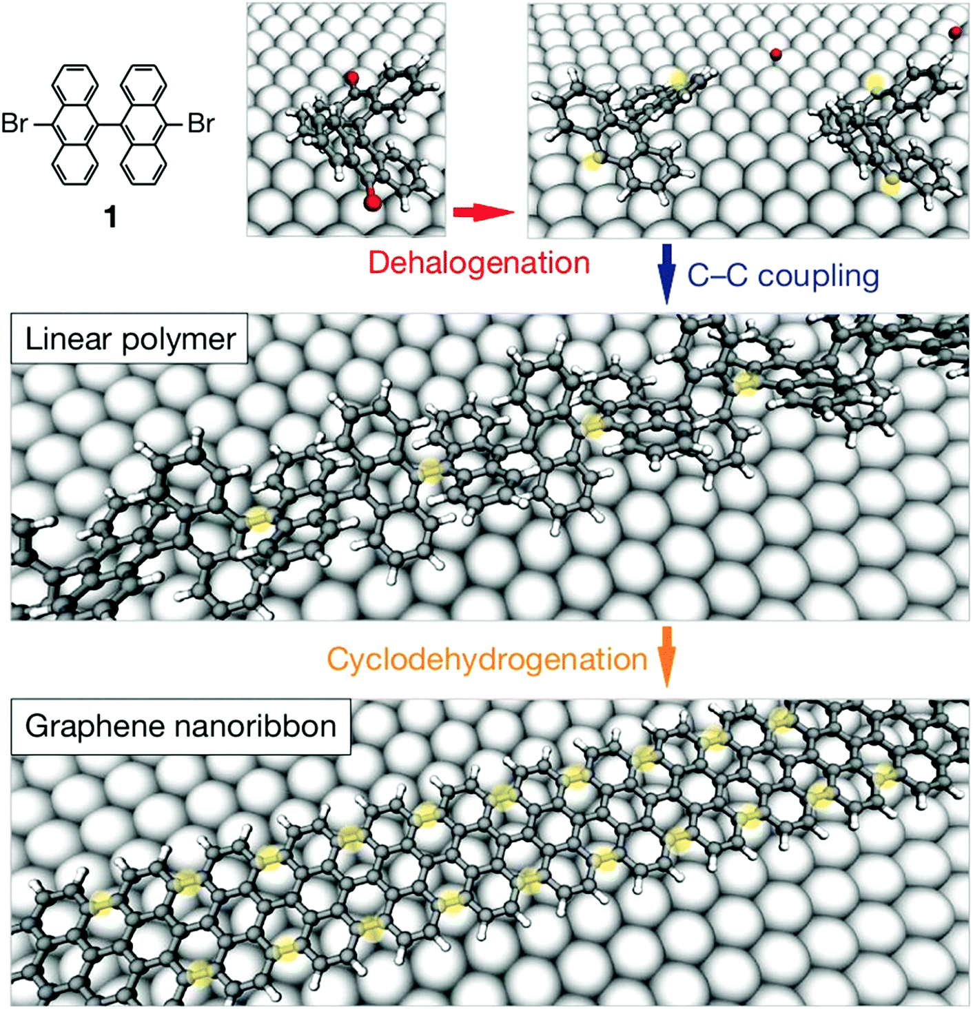 | ||
| Fig. 48 Bottom-up fabrication of synthetic graphene and GNRs starting from 10,109-dibromo-9,99-bianthryl monomers (1). Top, dehalogenation during adsorption of the precursor monomers. Middle, formation of linear polymers by covalent interlinking of dehalogenated intermediates. Bottom, formation of fully aromatic GNRs by cyclodehydrogenation.320 | ||
Chemical graphenes tend to form insoluble aggregates.662 A common strategy to solubilise conjugated systems is the lateral attachment of flexible side chains.956 This was very successful in solubilising small graphene molecules, while failing for graphenes with increasing size,956 because the inter-graphene attraction rapidly overtakes the solubilisation forces, making the current strategy less and less effective.956 A possible approach relies on supramolecular interactions that can be used to cover SLG with PAHs composed of (i) an aromatic core able to interact strongly with graphene and (ii) flexible side chains to make them soluble in most organic solvents. NGs adsorb reversibly forming ordered layers, with precise control of orientation and spacing.952,953 These interact with the graphene backbone allowing in principle to control and tune its optoelectronic properties,952 while the NG flexible side-chains makes the graphene-NG composites soluble.957
Supramolecular interactions have the advantage of keeping intact the sp2 network, without compromising the transport properties.956 Possible applications include the integration of graphene with other chemical functionalities, such as metal containing dye molecules or reactive sites for the attachment of biological molecules.
Chemical synthesis is also suited for the formation of superstructures, whose physics is very rich. E.g., the rotation angle between graphene layers controls the carrier velocity.958
There is much more to do in terms of designing and tuning the strength and type of interaction with the substrate. None of the superstructure-induced effects have been thus far harnessed in real devices. Several directions as starting points for the realization of such structures and effects can be planned. E.g., the induced growth across atomic islands of insulating materials deposited by nano-stencilling in regular patterns on catalytic, atomically flat metallic surfaces. Alternatively, exploring routes (e.g. thermally, electric field controlled or through electronic excitations) for the initiation of cascade chemical reactions and assembly from NG precursors on insulating monolayers and nanostructures to form graphene origami959 and GNRs. Such assembly has only been demonstrated so far on atomically flat metallic surfaces, but molecular self-assembly processes show considerable promise and versatility. Novel, volatile, metallo-organic and organometallic complexes could be used as the precursors for this process which will provide a route at the molecular level.
The aim is to explore synthetic graphenes starting from the compatibility with a very large range of substrates and the easy association of organic and inorganic layers. The target is to control with atomic precision the shapes and edges, in order to tune continuously the band gaps and conductivity, as well as control doping, obtaining a spatial distribution of dopants with ultimate resolution. Indeed, as the device size is pushed down, the dopant distribution needs to be precisely tuned, which is very difficult to achieve by post-treatment of large area graphene, such as hydrogenation or fluorination (or even doping during thin film growth). Precise and tailored dopant distribution may be assured by means of a hetero- (dopant) atom that is readily part of the precursor molecule. The effect of local doping needs to be investigated. This could be in principle achieved functionalising graphene using acceptor/donor molecules that would self-assemble precisely on its surface. Another challenges for direct chemical growth include growth on insulating substrates for electronic applications and development for efficient transfer methods that allow the nanoribbons to be incorporated in electronics.
4.9. Nano-ribbons and quantum dots
Ref. 296, 330 prepared GNRs by combining e-beam lithography and oxygen plasma etching. GNR down to ∼20 nm were reported, with band gap ∼30 meV, then used in FETs with ION/IOFF up to 103 at low T (<5 K) and ∼10 at RT. Ref. 329 reported much smaller GNRs, with minimum width ∼1 nm and gap ∼500 meV produced by e-beam lithography and repeated over etching. Sub-10 nm GNRs with bandgap up to 400 meV were produced via a chemical route,97 consisting in the dispersion of expanded graphite in liquid phase followed by sonication. Used as channels in FETs, they achieved ION/IOFF up to 107 at RT.303 A solution-based oxidative process was also reported,304 producing GNRs by lengthwise cutting and unravelling SWNTs and MWNTs.332 As result of the oxidative process, such GNRs show poor conductivity (∼35 S cm−1) and low μ (0.5–3 cm2 V−1 s−1) at RT.960Patterning of SLG into sub-10 nm GNRs with predetermined crystallographic orientation was achieved by STM lithography,307 by applying a bias higher than for imaging between the STM tip and substrate, while moving the tip at constant velocity.
GNRs can also be formed without cutting. Ref. 961 demonstrated that spatial selective hydrogenation can be used to create graphene “nanorods”, i.e. conductive paths of graphene surrounded by fully hydrogenated areas. Ref. 962 fabricated encapsulated ∼35 nm GNRs by depositing a polymer mask via scanning probe lithography, followed by chemical isolation of the underlying GNR by fluorinating the uncovered graphene. These GNRs retained μ of non-patterned graphene. Also, the fluorination is reversible, enabling write-erase-rewrite. GNRs down to 12 nm were produced by local thermal reduction of GO by scanning probe.963
Sub-10 nm GNRs were fabricated via catalytic hydrogenation, using thermally activated Ni nanoparticles as “knife”.310,964 This allows cutting along specific crystallographic directions, therefore the production of GNRs with well-defined edges.
GNRs were also made via LPE of GICs328 and expanded graphite.303 Growth on controlled facets on SiC resulted in 40 nm GNRs100 and the integration of 10000 top-gated devices on a single SiC chip.783
Chemical synthesis seems to be the most promising route towards well-defined GNRs,678 see Fig. 48. Atomically precise GNRs were produced by surface assisted coupling of molecular precursors into linear polyphenylenes and subsequent cyclo-dehydrogenation.678 GNRs up to 40 nm in length and soluble in organic solvents such as toluene, dichloromethane and tetrahydrofuran were synthesized336 from polyphenylene precursors having a non-rigid kinked backbone to introduce higher solubility in comparison to that of strictly linear poly(para-phenylene).965
Another route to GNRs is the so-called nanowire lithography,966 consisting in the use of nanowires as masks for anisotropic dry etching. GNRs smaller than the wire itself can be fabricated via multiple etching.966 Also, the wire, consisting of a crystalline core surrounded by a SiO2 shell, can be used as self-aligned gate.967
Arrays of aligned GNRs were produced by growing graphene by CVD on nanostructured Cu foils and subsequently transferring on flat Si/SiO2 substrates.968 The Cu structuring results in controlled wrinkling on the transferred material,968 which allows production of aligned GNRs by plasma etching.968
Besides their semiconducting properties, GNRs show other interesting properties, such as magnetoelectric effects.969 Also, half-metallic states can be induced in zigzag GNRs subjected to an electric field,325 chemically modified zigzag GNRs970 or edge-functionalized armchair GNRs.971 Half-metals, with metallic behaviour for electrons with one spin orientation and insulating for opposite, may enable current spin-polarization.325
Another approach to tune the bandgap of graphene relies in the production of QDs.956,972–977 These GQDs have different electronic and optical properties with respect to pristine graphene1,5 due to quantum confinement and edge effects.
Graphene oxide quantum dots (GOQDs) have been produced via hydrothermal972 and solvothermal973 methods (i.e. synthesis in an autoclave using aqueous and non-aqueous precursors, respectively) having lateral size ∼10 nm972 and ∼5–25 nm,973 respectively. Another route to produce GOQDs exploits the hydrazine hydrate reduction of small GO sheets with their surface passivated by oligomeric PEG.974 These GOQDs show blue PL for 365 nm excitation, while green PL for 980 nm excitation.974 GOQDs were also produced by electrochemical oxidation of a graphene electrode in phosphate buffer solution.975 These have heights between 1 and 2 nm and lateral size ∼3–5 nm.975 A bottom-up approach was used by ref. 976 to produce GQDs by metal-catalysed cage-opening of C60.
The fragmentation of the embedded C60 molecules at T ∼ 550 °C produced carbon clusters that underwent diffusion and aggregation to form GQDs.
As reported in section 4.9, GQDs can also be chemically synthesized, assembling PAHs,952,956 through surface mediated reactions. Ref. 977 exploited chemical synthesis to produce GOQDs by using an hexa-perihexabenzocoronene (HBC) precursor. GOQDs with ordered morphology were obtained by pyrolysis and exfoliation of large PAHs.977 The HBC powder was first pyrolyzed at a high T, then oxidized and exfoliated and reduced with hydrazine.977 The GOQDs had diameter ∼60 nm and thickness ∼23 nm, showing broad PL.977
4.10. Transfer and placement
Freestanding graphene membranes were first reported in ref. 134. Graphene samples were deposited by MC onto Si + SiO2 substrates, and then a grid was fabricated on them by lithography and metal deposition. Si was subsequently etched by tetramethylammonium hydroxide, leaving a metal cantilever with suspended graphene. This process was originally developed to fabricate suspended SWNTs.985Ref. 986 used the same approach to fabricate graphene membrane and study them by TEM, revealing that graphene sheets are not perfectly flat and exhibit intrinsic roughening. Ref. 987 fabricated mechanical resonators from SLG and FLG by mechanically exfoliating graphite over trenches in SiO2. Ref. 988 transferred graphene exfoliated either on SiO2 or polymer on TEM grids by first adhering to the grid and subsequently etching the substrate. Ref. 989 fabricated graphene membranes up to 100 μm in diameter by exfoliating graphite on a polymer and subsequently fabricating metal scaffolds on it by e-beam lithography and metal evaporation. The polymer was then dissolved leaving graphene membranes suspended on grids.989 A similar technique was used in ref. 990 to produce suspended samples to study graphene's optical transmission. Suspended graphene was obtained by contacting it via lithography and subsequently etching a trench underneath. This approach allowed to achieve ballistic transport at low T (∼4 K)145 and high μ (106 cm2 V−1 s−1).607 Suspending graphene drastically reduces electron scattering and samples suspended between contacts allowed observation of the fractional quantum Hall effect (FQHE).144,151
Graphene membranes have also potential for applications involving liquid separations, such as desalination, water filtration, DNA sequencing, as well as lab on chip microfluidic processes.991E.g., ref. 991 demonstrated that, when SLG is immersed in an ionic solution, it becomes an ionic insulators with a very small stable conductance that depends on the ion species in solution. This small effective thickness makes graphene an ideal substrate for very high resolution, high throughput, nanopore-based single-molecule detectors.991 The sensitivity of graphene's in-plane σ to its surface environment and trans-membrane solution potentials991 will offer new insights into atomic surface processes and sensor development opportunities.
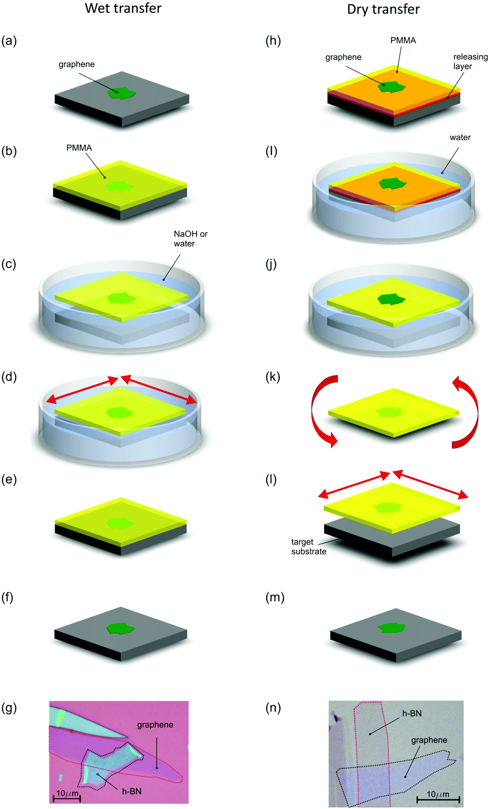 | ||
| Fig. 49 Wet (left) and dry (right) transfer of graphene. Wet transfer: (a) A graphene sample is deposited on oxidized Si by MC. (b) A PMMA film is deposited by spin coating (c) the PMMA film is detached from the substrate either via NaOH etching or water intercalation. Graphene adheres to the polymer and is removed from the Si + SiO2 substrate (d) PMMA + graphene film is “fished” using the target substrate. By sliding the PMMA + graphene film with respect to the substrate a flake of choice can be aligned with features such as electrodes, cavities, etc. (e) Once the sample has dried, PMMA is dissolved by acetone releasing the graphene on the target substrate (f). (g) A graphene flake deposited onto BN by wet transfer. Dry transfer: (h) graphene is exfoliated onto substrates covered by a polymer stack consisting of a water-dissoluble polymer (such as PVA) at the bottom and PMMA on the top. (i) The sample is left to float in a water bath in such a way that the “release” layer is dissolved from the side. (j) Graphene is on top of the stack and is never in touch with water (k) the polymer + graphene film is attached to a special holder and flipped over. (l) By means of a manipulator the flake of choice is placed in the desired position on top of the desired substrate, then the film is pressed on the target substrate (m) PMMA is dissolved leaving graphene in the desired position (n) graphene layer deposited onto a BN flake by dry transfer. Adapted from ref. 602. | ||
Ref. 995 reported the deterministic placement of graphene by exploiting a thin layer of water between the PMMA/graphene foil and the substrate. Ref. 996 reported transfer of nanostructures (including graphene) embedded in a hydrophobic polymer. Also in this case, intercalation of water at the polymer–substrate interface was used to detach the polymer/nanostructures film, then moved on a target substrate.402
PMMA is a positive resist widely used for high resolution e-beam lithography.403 By patterning PMMA, it is also possible to remove unwanted graphitic material surrounding MC-SLGs, while shaping and isolating the flakes of interest.
The Van der Waals interaction between 2d materials was used to assemble heterostructures such as BN-SLG-BN.999Fig. 50 shows a schematic of the process where an isolated few layer BN flake is used as a stamp to successively pick up alternating layers of monolayer graphene and few-layer BN.999 An advantage of this technique compared with other transfer methods is that the active interfaces do not contact any polymer throughout the process, reducing impurities trapped between the layers.999
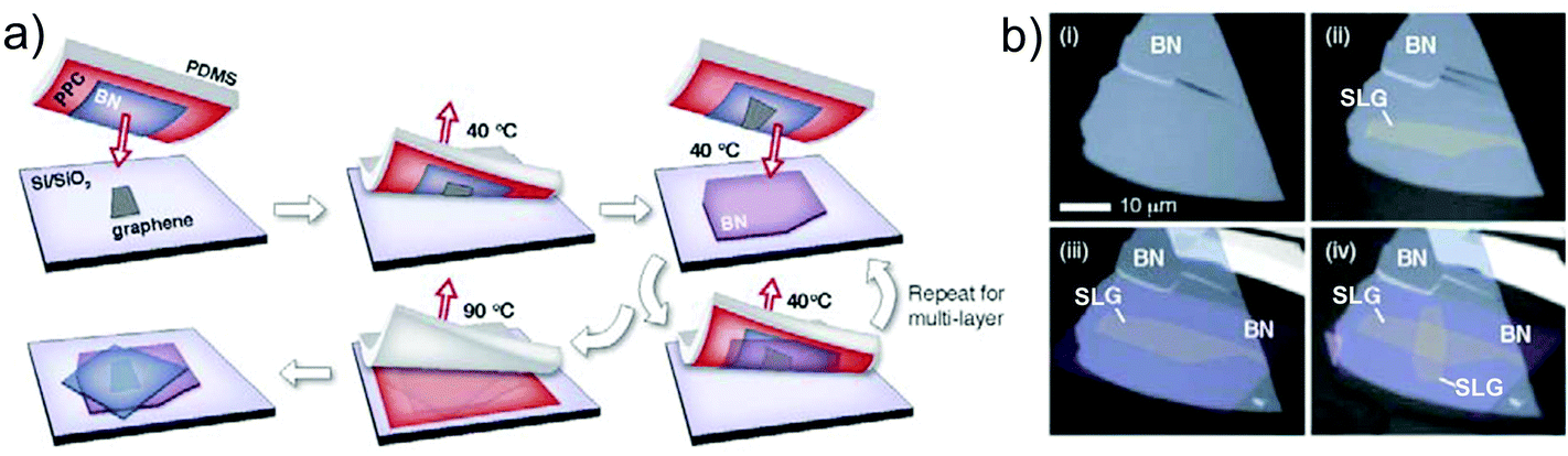 | ||
| Fig. 50 Layer by layer assembly process. (a) Schematic diagram showing the steps to make a BN-SLG-BN stack or a multiple-layer stack with device layer (graphene) never exposed to any polymer or solvent. (b) Optical images showing in sequence a BN flake on poly-propylene carbonate (PPC) and film picking. Adapted from ref. 999. | ||
A big challenge is the development of a dry transfer technology for ultrahigh quality graphene up to 450 mm, avoiding the wet conditions with polymer coating, which suffer from polymer contamination. The development of dry processes for large area graphene on insulator would be extremely useful for long-term sustainability in device engineering.
Optical trapping can also be exploited to manipulate (translate, rotate) and deposit trapped graphene250,669 and 2d crystals on solid substrates in a controlled fashion.
Optical binding, the formation of extended periodic self-organized (optically bound) structures, could be used for patterning and controlled deposition on a substrate over an extended area for parallel nano-lithography. Another promising application of radiation forces is optical stamping lithography,1000 where the repulsive force exerted by a laser beam is exploited to deposit flakes at desired positions on a substrate. Exploiting this, graphene flakes could be optically stamped on substrate using holographic patterns (with a Spatial Light Modulator), and combined with any other nanomaterial.669 This paves the way for microfluidic integration, expanding the applicability for biosensing.
To avoid Fe contamination caused by FeCl3 etching, ammonium persulfate [(NH4)2S2O8] was used.1001 To avoid mechanically defects caused by R2R transfer, a hot pressing process was developed:1002 similar to a R2R process, the Cu + graphene foil is first attached to thermal release tape and then Cu is chemically etched. The tape + graphene foil is then placed on the target substrate and they are inserted between two hot metal plates with controlled temperature and pressure. This results in the detachment of the adhesive tape with very low frictional stress, therefore less defects, than a R2R process.1002
In 2003 ref. 1005 reported large area deposition of SWNTs between electrode pairs by DEP.410 Subsequently, DEP was used for the separation of metallic (m-SWNTs) and semiconducting single wall nanotubes (s-SWNTs),1006 exploiting their dielectric constants difference, resulting in opposite movement of m and s-SWNTs.1006 These SWNT processes were then adapted for graphene. Ref. 1007, 1008 used DEP for the manipulation of GO soot, and single and few-layer GO flakes. In 2009 ref. 1009 placed individual FLGs between pre-patterned electrodes via DEP. Once trapped, the higher polarizability of graphene compared to the surrounding medium1009 limits the deposition to one flake per device.1009,1010 Self-limiting is one of the advantages of this method, together with the direct assembly of individual flakes at predetermined locations.
Rod-coating employs a wire-wound bar, also known as Mayer bar (invented by Charles W. Mayer, who also founded the Mayer Coating Machines Company in 1905 in Rochester, USA).1012 This is a stainless steel rod wound with a tight wire spiral, also made of stainless steel. During coating, this creates a thin (∼tens μms) ink layer on a substrate.1013 Spray coating forms aerosols of the liquid ink, resulting in uniform thin (∼μm) films on a substrate.1012 Screen printing, on the other hand, uses a plate or screen containing the pattern to be printed on the substrate.1012 The screen is then placed onto the target substrate, while the ink is spread across the screen using a blade, thus transferring the pattern.1012 Flexo- and gravure1015 printing also use a plate to transfer images onto target substrates. Flexo uses a relief plate, usually made of flexible polymeric material, where the raised sections are coated with ink, then transferred onto the substrate by contact printing.1012 Gravure uses an engraved metallic plate, consisting of dots representing pixels.1012 The physical volume of the engraved dots defines the amount of ink stored in them,1016 thus can be used to create gray-scale patterns/images.1016 In general, different viscosities are preferred for different R2R techniques, ranging from 1 to 10000 mPa s or above,1012,1016. Rod- or spray-coating form uniform films, that may be used for larger scale devices (>several cm), the fabrication of TCs, or devices such as batteries or supercapacitors. Screen (∼50–100 μm resolution1012), flexographic (∼40 μm resolution1012) and gravure (∼15 μm resolution1012) printing can be used to print different materials with specific patterns for flexible electronics.1016 For resolutions down to ∼50 μm, inkjet printing offers a mask-less, inexpensive and scalable low-T process.1017 The resolution can be significantly enhanced (<500 nm) by pre-patterning,1017 so that the functionalized patterns can act as barriers for the deposited droplets.1017 The volume can be reduced to atto-liters/drop by pyroelectrodynamic printing.1018 The process is based on the control of local pyroelectric forces, activated by scanning a hot tip or a laser beam over a functionalized substrate (e.g. lithium niobate1018), which draw liquid droplets from the reservoir and deposit them on the underside of the substrate.1018
All of the above techniques can be applied to graphene inks/dispersions. Large scale placement of LPE graphene can be achieved via vacuum filtration,35 spin706 and dip coating,1788 Langmuir–Blodgett662 and spray coating.622 Amongst the R2R techniques, rod-coating has been demonstrated to fabricate TCs.995 Inkjet printing of pristine graphene dispersions was also demonstrated.63 Inkjet printing1019 permits selective deposition and high concentration for partially soluble compounds.1020Ref. 629 reported an inkjet printed graphene TFTs with μ up to ∼90 cm2 V−1 s−1 and Tr ∼ 80%. Inkjet printing of GO was also demonstrated,1021–1024 To minimize clustering of the graphene flakes at the nozzle edge, the flakes should be smaller than 1/50 of the nozzle diameter.629
Inkjet-printing was demonstrated a viable technique to obtain high conductivity graphene patterns.1025 The ink was prepared exploiting ethanol as solvent and ethyl cellulose as stabilizer.1025 The inkjet-printed graphene features had low resistivity of 4 mΩ cm, with uniform morphology, compatibility with flexible substrates, and tolerance to bending stresses.
4.11. Contamination and cleaning
Cleaning is a critical part of semiconductor device processing.1026 It is usually performed after patterning and etching processes leave residues.1026 Wet chemical etches are also performed to remove damage from surfaces.1026 Most applications require graphene on a dielectric surface. When graphene is grown directly on a dielectric as in the case of graphene on SiC [see section 4.2] or when graphene or GO is deposited on the dielectric substrate directly [see section 4.12.3], cleaning is required only after patterning and etch processes, as devices are fabricated. Because every atom is a surface atom, graphene is very sensitive to contaminants left by production, transfer or fabrication processes. In order to remove them, several methods have been developed.4.11.1. Cleaning of graphene produced by MC
The amount of contamination can be assessed optically.1027 Organic contamination arising from the diffusion of tape glue used in MC changes the contrast.1027 TEM and scanning probe,1028,1029 microscopy (e.g. AFM, STM), Raman185,1030 together with transport measurements1030 are other viable techniques to detect contaminants on graphene films or flakes. Ref. 1028 cleaned MC samples from resist residuals by thermal annealing (at 400 °C, in Ar/H2), assessing the quality of the cleaning process via scanning probe techniques. Ref. 1029 introduced thermal annealing (at 280 °C) in ultra-high vacuum (<1.5 × 10⁻¹⁰ Torr), to remove resist residues and other contaminants. Ref. 1028 cleaned graphene by using high current (∼108 A cm−2). This allows removal of contamination in situ, and is particularly useful when graphene devices are measured in a cryostat.103 Chemical cleaning by chloroform was reported in ref. 1030. Mechanical cleaning by scanning the graphene surface with an AFM tip in contact mode was also reported.1031In graphene transfer from metals to dielectric surfaces, organic materials such as PMMA or perylene-3,4,9,10-tetracarboxylic dianhydride (PTCDA) are typically used as the carrier material, with subsequent chemical removal, e.g. by acetone.6,865Ref. 1033, 1034 detected by XPS the presence of residue on the surface of graphene grown on Cu and transferred onto SiO2. The C1s spectrum was found broader than that of graphite and the original graphene on Cu. The broadening was associated with the presence of the residue. Upon annealing in high vacuum (10−9 mbar) at T ∼ 300 °C, the C1s width decreased to a value close to the original graphene on Cu.1033,1034 The use of thermal release tape7 (i.e. a tape adhesive at RT, but that peels off when heated), instead of PMMA or PTCDA, is more problematic, since tape residues can contaminate the sample.7 There is some anecdotal evidence that the presence of residue has a beneficial effect on the nucleation of ALD dielectrics, such as Al2O3.1035 However, this approach to prepare the graphene surface for ALD is not ideal, since the residues have uncontrolled chemical nature and are not uniform. Ref. 1036 developed a modified RCA transfer method combining an effective metal cleaning process with control of the hydrophilicity of the target substrates. RCA stands for Radio Corporation of America, the company that first developed a set of wafer cleaning steps in the semiconductor industry.1026Ref. 1036 demonstrated that RCA offers a better control both on contamination and crack formation with respect to the aforementioned approaches.6,7,865
624 or air.642 The latter process could help remove residual surfactant molecules.624,642 However, there is no “fixed” T for solvents/surfactants removal, and the different conditions/requirements are ruled by the boiling/melting points of each solvent/surfactant.
4.12. Inorganic layered compounds
This allowed the structural characterisation of BN by high resolution TEM1038 and its use as a substrate for high performance graphene devices.908 Similarly, for MoS2 a number of advances have been demonstrated including the production of sensors,1042 transistors5,379,1043 and integrated circuits,1044 the measurement of the mechanical properties of individual nanosheets409 and the observation of the evolution of the vibrational421 and electronic structure,378 with number of stacked flakes.
As in the case of MC of graphite, MC of LMs is not industrially scalable, and MC-flakes are mostly suited for fundamental studies and proof of principle devices.
The exfoliation and dispersion of LMs were also carried out by the exploitation of co-solvents where the dispersibility of LMs can be greatly improved by using a mixture of solvents1051,1056e.g., water–ethanol,1051,1056 water–isopropyl alcohol,1056etc. By adjusting the relative concentration of the co-solvents it is possible to tune the rheological properties1057 of the mixture “on demand”. However, YM and concentration of the exfoliation process in such co-solvent mixtures is, up to date,1051,1056 much lower than in NMP629 and water-surfactant dispersions.250 Exploitation of co-solvent mixtures,1051,1056,1057 mostly based on water and alcohols, for the dispersion and exfoliation of LMs has some practical disadvantages.1058 The surface tension changes exponentially after the addition of alcohols to water,1057 thus being very sensitive to solvent evaporation.1056 The rheological properties of alcohol-based co-solvents are very temperature sensitive.1057 This is a problem both during processing (the ultrasonication causes a temperature increase of the dispersion) and for the shelf-life (i.e. the maximum time for which the inks can be stored without alteration of their properties) of the dispersions/inks.
Much work remains to be done: exfoliation techniques must be extended to a wider range of materials. Both solvent38 and surfactant-exfoliated396 TMDs tend to exist as multilayer stacks with few individual sheets, thus requiring an improvement of the exfoliation. The dispersed concentrations (up to tens of grams per litres) and the lateral flake size (up to mm) still need to be increased considerably.
In order to pursue these requirements, the development of a sorting strategy that may allow to control both lateral dimensions and N is necessary for the full exploitation of their optical and electronic properties.
Quantitative analysis for monitoring the exfoliation (yield and quality of the as-produced material) of TMDs and TMOs is based on a range of techniques such as AFM, TEM, Raman spectroscopy, etc.2337N can also be controlled via separation in centrifugal fields or by combination with DGU.602,642
The availability of dispersions opens up a range of applications in composites, thin films and inks that can be printed in a variety of ways, and mixed to create hybrids. Many applications in photonics and optoelectronics, such as TCs, third generation solar cell electrodes, and optical-grade composites benefit from LPE produced and assembled materials.
LPE can also produce ribbons with widths <10 nm,303 allowing a further in-plane confinement of the 2d crystals, thus an extra handle to tailor their properties. LPE does not require transfer techniques and the resulting material can be deposited on different substrates (rigid and flexible) following different strategies, such as dip and drop casting, spin, spray and rod coating, ink-jet printing, etc. Several LMs (including BN, MoS2, WS2, MoSe2, MoTe2, TaSe2, NbSe2, NiTe2, and Bi2Te3) have been already successfully exfoliated using this simple, yet efficient, method38 that potentially brings also a benefit in terms of chemical stability, as the layer of liquid might protect the crystallites from oxidation. Such suspensions allow, lastly, easy assembling of the materials into superstructures.
To date, WS2 films have been deposited by magnetron sputtering from both WS1061 and WS2 targets,1062 sulfurization of W1063 or WO2 films,1064 ion beam mixing,1065etc. The preferred production process for tribological applications is magnetron sputtering,1066 because of its lower T than thermally activated deposition methods.1066 This is also well suited for large area deposition (∼m2).1067 CVD was used to grow h-BN,1068 and is now being developed to grow TMDs.1069 If single layers of the binary films are desired, then ALD or, more appropriately, ALE might be a better suited.
4.13. Graphene and other 2d crystal hybrids
Technological progress is determined, to a great extent, by developments in material science. The most surprising breakthroughs are attained when a new type of material, or new combinations of known materials, with different dimensionality and functionality, are created. Well-known examples are the transition from 3d semiconducting structures based on Ge and Si to 2d semiconducting heterostructures, nowadays the leading platform for microelectronics. Ultimately, the limits and boundaries of certain applications are given by the very properties of the materials naturally available to us. Thus, the band-gap of Si dictates the voltages used in computers, and the Young's modulus of steel determines the size of the construction beams. Heterostructures based on 2d crystals will decouple the performance of particular devices from the properties of naturally available materials. 2d crystals have a number of exciting properties, often unique and very different from those of their 3d counterparts. However, it is the combinations of such 2d crystals in 3d stacks that offer vast opportunities in designing the functionalities of such heterostructures. One can combine conductive, insulating, probably superconducting and magnetic 2d crystals in one stack with atomic precision, fine-tuning the performance of the resulting material. Furthermore, the functionality of such stacks is “embedded” in the design of such heterostructures.Heterostructures have already played a crucial role in technology, giving us semiconductor lasers and high μ FETs. However, thus far the choice of materials has been limited to those which can be grown (typically by MBE) one on top of another, thus limiting the types of structures which can be prepared. Instead, 2d crystals of very different nature can be combined in one stack with atomic precision, offering unprecedented control on the properties and functionalities of the resulting 2d-based heterostructures. 2d crystals with very different properties can be combined in one 3d structure, producing novel, multi-functional materials. Most importantly, the functionality of such heterostructures will not simply be given by the combined properties of the individual layers. Interactions and transport between the layers allow one to go beyond simple incremental improvements in performance and create a truly “quantum leap” in functionality. By carefully choosing and arranging the individual components one can tune the parameters, creating materials with tailored properties, or “materials on demand”. Following this novel approach, part of the functionality is brought to the level of the design of the material itself.
Inorganic LMs can be exploited for the realization of heterostructures with graphene, to modulate/change the electronic properties, thus creating “materials on demand”: hybrid superstructures, with properties not existing in nature,99,106,1070,1078 tailored for novel applications. E.g., superstructures like those in Fig. 31 (SLG/BN/MoS2/BN/SLG) can be used for tunnel devices, such as diodes, FETs, and light emitting devices, or for energy application, such as photovoltaic cells.
To date, 3 methods can be envisaged for the production of atomically thin heterostructures: (I) growth by CVD;1071 (II) layer by layer stacking via mechanical transfer,99,908,1072 and (III) layer by layer deposition of chemically exfoliated 2d crystals. However, as the field develops, other techniques will emerge.
CVD is emerging as a promising approach to grow 2d crystals. Growth of h-BN1073 and MoS21074 was already demonstrated. Ref. 1073 reported growth of single layer h-BN by thermal decomposition of borazine (B3N3H6) on Ni (111). Ref. 1074 demonstrated that the CVD growth of MoS2 is scalable and films of any size can be made because the lateral size of the layers is defined by the size of the substrates used. Moreover, also the thickness of the MoS2 film can be controlled being directly dependent on the thickness of the pre-deposited Mo metal on the substrate and the as-grown layers can then be transferred onto arbitrary substrates.1074
The aim is to produce a large range of 2d crystals on large scale and with control on demand of N. Low-T CVD and CMOS compatible substrate will be investigated as well all the transfer strategies already developed with graphene.
2d crystals can also be produced as nanoribbons (NRs) with tuneable electrical and magnetic properties. MoS2-NRs were made via electrochemical/chemical synthesis,1075 while zigzag few- and single-layered BN-NRs were obtained unzipping multiwall BN nanotubes through plasma etching.1076 The target is to produce, within the next 10 years, NRs with controlled electrical and optical properties.
Field effect vertical tunnelling transistors based on graphene heterostructures with atomically thin BN acting as a tunnel barrier, were reported.489 The device operation relies on the voltage tunability of the tunnel density of states in graphene and of the effective height of the tunnel barrier adjacent to the graphene electrode.489Ref. 491 used WS2 as an atomically thin barrier, allowing switching between tunnelling and thermionic transport, with much better transistor characteristics with respect to the MoS2 analogue,489 thus reaching a much higher ION/IOFF ∼ 106. A “barristor”, i.e. a graphene-Si hybrid three-terminal device that mimics a triode operation, was developed by ref. 492. The electrostatically gated graphene/Si interface induces a tunable Schottky barrier that controls charge transport across a vertically stacked structure.489,491,492
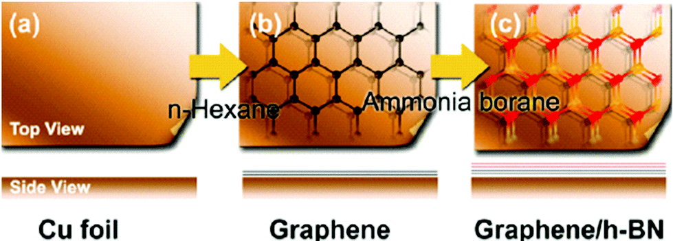 | ||
| Fig. 51 Schematic of Graphene/BN stacked film. (a) The Cu foil is cleaned and prepared as the growth substrate. (b) High-quality and large-area graphene film is grown via CVD with n-hexane as a liquid carbon source at 950 °C. (c) The as-grown graphene is then loaded into another furnace for the growth of h-BN film on top. Adapted from ref. 1077. | ||
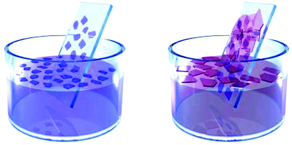 | ||
| Fig. 52 Superstructure assembly by dispersions and inks. Dip casting is used to deposit successive layers of different 2d crystals to create an heterostructure. | ||
Although the quality of the resulting structures would be significantly lower than that obtained by mechanical or CVD methods, it would still be suitable for a number of photonics and optoelectronics applications, as well as for applications in thin film transistors, RF tags, solar cells, batteries and supercapacitors.
4.14. Silicene, germanene, phosphorene, MXene and other graphene like systems
Silicene sheets,113,114i.e. the Si equivalent of graphene,1081 see Fig. 53a, have been synthesized by in situ growth on silver (Ag) (111) surfaces. A honeycomb atomic structure with a Si–Si distance of 0.23 nm was revealed in STM,113,1081 with a long-range epitaxial order confirmed by sharp LEED patterns. Conical band dispersions at the corners of the silicene Brillouin zone (K and K′ points), evidenced in High-Resolution ARPES measurements, point to Dirac fermions with a Fermi velocity of 1.3 × 10⁶ ms−1, as theoretically predicted,1082 quite the same as graphene, and four times higher than previously obtained on a 1d grating of silicene NRs.1083 GGA-DFT calculations including the Ag(111) substrate-confirm the stability of the epitaxial arrangement. | ||
| Fig. 53 (a) STM image showing the graphene-like structure of one monolayer of silicon deposited on a closepacked silver surface, Ag (111). Adapted from ref. 114 (b) 16.2 nm × 16.2 nm STM image of the modulated honeycomb of germanene √7 × √7 superstructure with a zoom-in at the bottom left corner (the √7 × √7 unit cell is drawn in black). Adapted from ref. 1099; (c) Side view of MXene, where M (green dot) is an early transition metal, X is either carbon and/or nitrogen (grey dots) and A is an A-group (mostly IIIA and IVA, or groups 13 and 14) element. Adapted from ref. 1100. | ||
Silicene is predicted to have non-trivial topological properties.115 Hence, it could offer the possibility, if interfaced with a s-wave superconductor, for advances in the long quest for Majorana fermions.270 Furthermore, being Si the workhorse of electronics, this synthesis could have a impact for novel devices because of the compatibility with existing Si technologies. A key issue in this direction is the transfer -or even the growth-on an insulating substrate, like, e.g., AlN.1082
The growth of silicene paves the way to the synthesis of germanene, see Fig. 53b, the equivalent of graphene for Ge, also with nontrivial band topology, and a gap induced by effective spin orbit coupling for the π orbitals at the K point.270,115
Stanene, a single layer of tin atoms,123 arranged in a manner similar to graphene, was observed in MBE experiments in the nineties.117 Stanene deposited on substrate has a gap ∼0.3 eV,123 with quantum spin Hall (QSH) states (i.e. edge states where the carriers with opposite spins move in opposite directions1084) states that can be tuned by chemical functionalization as well as by external strain.123
Phosphorene is a stable elemental 2d material that can also be mechanically exfoliated from bulk black phosphorus,116 which is the most RT stable phosphorus allotrope.1085 Black phosphorus was first synthesized from white phosphorus (also known as tetraphosphorus, a molecule made up of four atoms in a tetrahedral structure) under high pressure and high temperature in 19141086 and it has a layered structure, held together by vdW forces.1087–1089 Black phosphorus displays a sequence of structural phase transformations, superconductivity at high pressures with Tc above 10 K, and T dependent resistivity and magnetoresistivity.1090–1095 Phosphorene layers share a honeycomb lattice structure with graphene with the notable difference of non-planarity in the shape of structural ridges. The bulk lattice parameters of black phosphorus are: a1 = 3.36 Å, a2 = 4.53 Å, and a3 = 11.17 Å (ref. 116). The large value of a3 is caused by the nonplanar layer structure and the presence of two AB stacked layers in the bulk unit cell, see Fig. 26. The ridged layer structure helps to keep orientational order between adjacent phosphorene monolayers and thus maintains the in-plane anisotropy.116
Another class of 2d crystals are the MXenes, i.e. transition metal carbides and nitrides, see Fig. 53c, created by selectively removing Al (in hydrofluoric acid at RT)119 from layered ternary carbides known as MAX phases. These could add at least another 60 members to the LM family.119,120 Through this exfoliation process, the carbide layers were separated into two MXene sheets just a few atoms thick.119 MXenes can accommodate various ions and molecules between their layers by intercalation.1096,1097 MXene sheets are promising for energy applications, such as Li-ion batteries,1096 electrochemical capacitors120,1097 and hydrogen storage.1098Ref. 1097 reported the spontaneous intercalation of cations from aqueous salt solutions between 2d Ti3C2 MXene layers. A variety of cations, including Na+, K+, NH4+, Mg2+, and Al3+, can also be intercalated electrochemically, offering capacitance in excess of 300 F cm−3, a value that is much higher than that achieved by porous carbons1097 and comparable with those reported in other GRMs, see section 10.2.
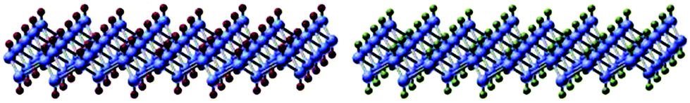 | ||
| Fig. 54 Chemically modified graphene. One can add different species (e.g. hydrogen, purple dots or fluorine, green dots) to the graphene scaffolding. | ||
Ref. 122 synthesized millimeter-scale crystals of a hydrogen-terminated germanane from the topochemical deintercalation of CaGe2. This layered solid is analogous to multilayer graphane.33 The resultant four-coordinate puckered lattice of Ge atoms has an analogous geometry to the sp3-hybridized graphane surface, in which every Ge atom is terminated with either H or OH above or below the layer.124 The surface layer of germanane only slowly oxidizes in air, after 5 months.122 Germanane is thermally stable up to 75 °C (ref. 122). However, above this T, dehydrogenation and amorphization begin to occur.122 Germanane is the first of a new class of covalently terminated graphane33 analogues, that could cover a variety of traditional semiconductors, and has potential for a wide range of (opto)electronic and sensing applications, because of its direct band gap of 1.53 eV (ref. 122) and an electron μ ∼5 times higher than that of bulk Ge (3900 cm2 V−1 s−1), as predicted by theory.122
4.15. Outlook and future challenges
The successful use of GRMs depends not only on the identification of the right products for new and current applications, but also on the ability to produce any of the materials in large quantities at a reasonable cost. We now know over 600 LMs exist, and probably more. The progress in developing new materials processes over the past few years has been impressive.However, the suitability of any given process depends on the application. Nanoelectronics more than likely has the most demanding requirements, i.e. low defect density single crystals. Other applications, such as biosensors, may require defective graphene, while printable electronics can tolerate lower quality, e.g. lower μ, graphene. CVD techniques are emerging as ideal for large area graphene films for touch screen displays and other large display applications, while graphene derived from SiC maybe better suited for resistor standards. Many issues still remain to be addressed in the growth of graphene by CVD to improve the electrical and optical characteristics, including mechanical distortions, stable doping, and the development of reliable low cost transfer techniques. While transfer techniques can be developed to place graphene onto insulating substrates, it is desirables to grow graphene directly on dielectric surfaces for many device applications and progress is being made in achieving films on h-BN as well as SiO2. However, a lot more effort is required to achieve large area uniform high quality graphene films on dielectrics. In the case of graphene on SiC, among other issues related to uniformity, crystal size could be an impediment for large scale production. LPE is appealing for inks, thin films and composites, and future research is needed to control on-demand N, flake thickness and lateral size, as well as rheological properties. Synthetic graphenes, together with GNR produced by SiC,100 are promising for the production of atomically precise NRs and QDs to overcome the lack of band gap necessary for many electronic device applications. A controlled dopant distribution is also needed, and techniques such as functionalization using self-assembled acceptor/donor molecules or assembling pre-doped molecules are being studied.
The layered nature of graphite makes its integration with other LMs a natural way to create heterostructures. LMs have been around for a long time and studied and developed mostly for their tribological properties. Now these materials are being considered as new interlayer dielectrics for heterostructures with potential for new electronic devices with exotic properties. Because of this, there will be a host of new processes that will need to be developed in order to grow or deposit high quality large area monolayer films integrated with graphene with controlled thickness and transport properties.
The GRMs production timeline is shown in Fig. 55. Timescales: 2–3 years: Formulation of GRM inks. CVD growth high μ (6 × 104 cm2 V−1 s−1) graphene films. Homogeneous (mm2) graphene films on SiC 3–5 years: Production of heterostructures with on-demand (opto)electronic properties via LPE and CVD. 5–7 years: Production of 2d crystal by MBE and ALD. Formulation of high concentration inks (10 g L−1) with tuneable morphological (>80% 1-L) and controlled rheological properties (ν = 1–1000 mPa s). 7–10 years: Production of large area (mm size) 2d crystals via LPE. Large area single crystals. Surface roughness <0.2 nm. Engineered band gap NRs and QDs.
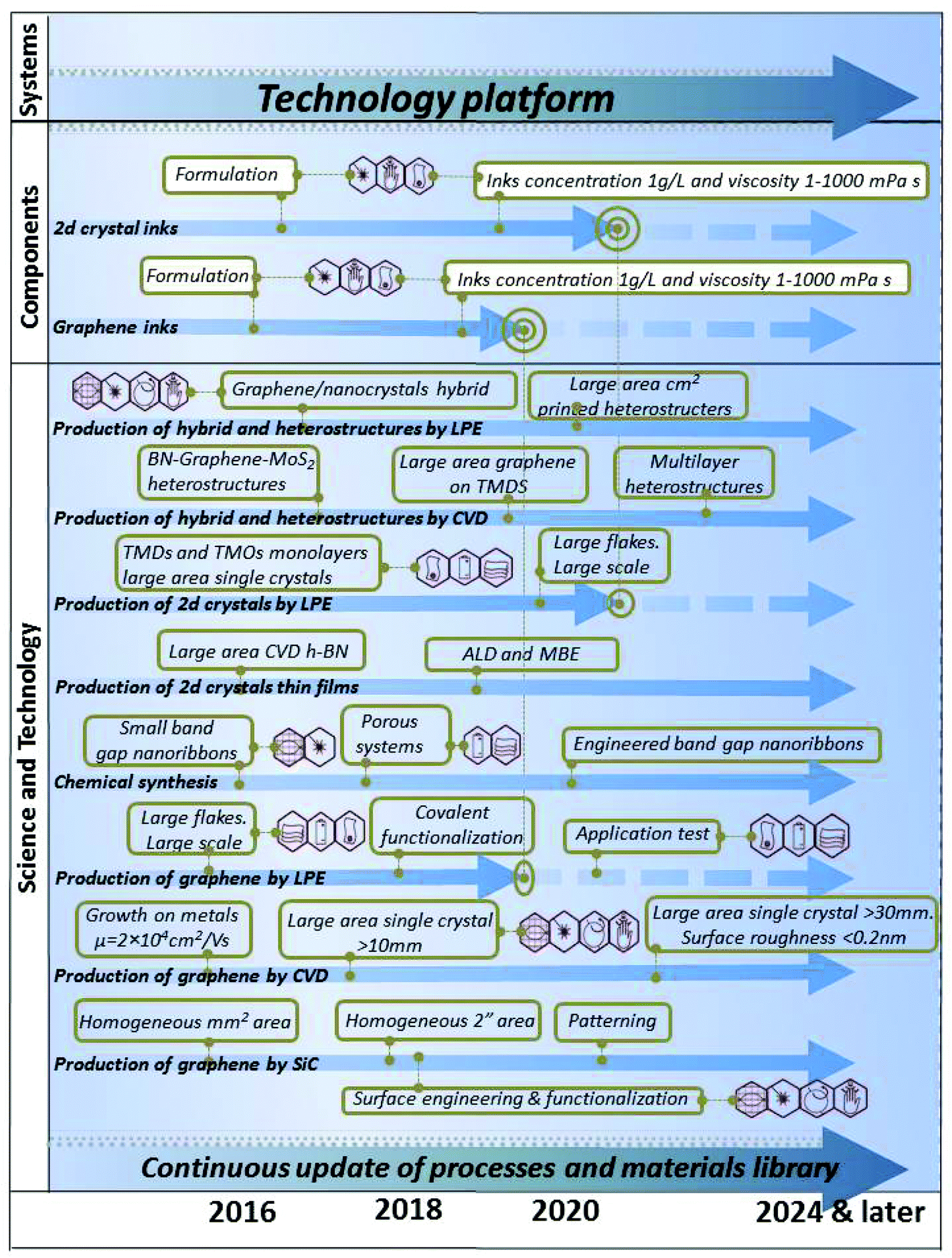 | ||
| Fig. 55 GRM production timeline. | ||
5. Electronic devices
Graphene has already demonstrated high potential to impact most ICT areas, ranging from top-end, high-performance applications in ultrafast (>1 THz) information processing, to consumer applications using transparent or flexible electronic structures.The great promise of graphene is testified by the increasing number of chip-makers now active in graphene research. Most importantly, graphene is considered to be amongst the candidate materials for post-Si electronics by the ITRS.12
5.1. Opening a band-gap in graphene
The target is to fully explore the performance of graphene transistors in both logic and RF applications. Graphene may be used to develop new applications based on stretchable electronics, such as conformal biosensors and rollable displays. These are required to meet the increasing needs of human-interface technology. Graphene can solve the standstill of stretchable electronics, due to the difficulty in developing semiconducting materials with the high stretchability required for such applications. Fig. 56 and Table 3 show some possible applications and an indication of when functional device prototypes could be expected.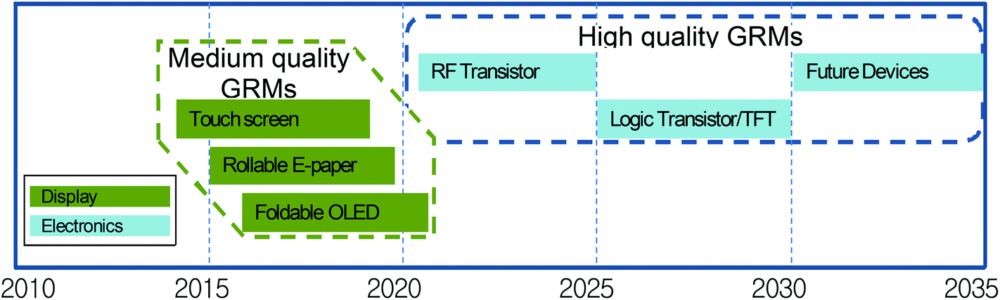 | ||
| Fig. 56 GRM electronics’ application timeline. The rectangles in the figure indicate the timeframe when functional device prototypes could be expected. | ||
| Application | Drivers | Issue to be addressed |
|---|---|---|
| Touch screen | Better endurance with graphene as compared to other materials | Need to better control contact resistance |
| E-paper | High Tr of SLG; Visibility | Need to better control contact resistance |
| Foldable OLED | Graphene with high electrical properties and bendability | Need to improve the Rs |
| Efficiency improved due to graphene's work function tunability | Need to control contact resistance | |
| Atomically flat surface of graphene helps to avoid electrical shorts and leakage current. | Need a conformal coverage of 3d structures | |
| RF Transistor | No manufacturable solution for InP high-electron-μ transistors (HEMT) (low noise) after 2021 according to the 2011 ITRS | Need to achieve current saturation |
| f T = 850 GHz, fmax = 1200 GHz should be achieved | ||
| Logic Transistor | High μ | New structures |
| Need to resolve the band-gap/μ trade-off | ||
| Need ION/IOFF >106 |
Graphene can replace materials in several existing applications, but the combination of its unique properties should inspire completely new applications, which is the ultimate target.
The major obstacle of graphene in transistor applications, especially for ICs as potential Si replacement, is its zero band-gap. This is responsible for the low ION/IOFF in GFETs due to a non-zero off state drain current, which leads to considerable static power dissipation. E.g., the typical static drain current in graphene inverters1102 is ∼270 μA μm−1 at a supply voltage VDD = 2.5 V, in contrast to the much smaller leakage drain current ∼100nA μm−1 at VDD = 0.75 V in 22 nm node high-performance Si logic transistors.1103 Small band gap opening was observed in large area hybrid films, consisting of graphene and h-BN domains synthesized on Cu substrates by CVD.1104
Thus, opening a band gap without compromising any of its other outstanding properties, such as high-field transport and μ, is one of the most active research areas. Apart from quantum confinement (GNRs and GQDs), many other techniques have been developed for this goal. Substrate induced band-gap opening was investigated.1105 Band-gap opening in graphene, both on h-BN and h-BN/Ni(111) with band gap up to 0.5 eV was reported.1106 Theory suggests that a band gap ∼0.52 eV can be opened in graphene deposited on oxygen terminated SiO2 surfaces.1107 A bandgap is observed for BLG grown on SiC.1108
Substitutional doping is another promising route for opening a band gap. Nitrogen doping might be used to convert graphene into a p-type semiconductor.1109
A few other approaches also exist for band gap engineering. Formation of GNRs with finite band gaps is possible using conventional BC lithography.339 A band gap ∼0.7 eV was demonstrated by selective hydrogenation of graphene on Ir.358 Molecular doping and charge transfer methods could also modulate the electronic properties via paramagnetic adsorbates and impurities that can dope graphene.1110 Selective chemical functionalization can also be used for band gap engineering.33,34 Complete hydrogenation of graphene forms graphane, an insulator,33 while a similar process using Fluorine, produces fluorographene.34 The latter is optically transparent with a gap ∼3 eV.34 If an electric field is applied perpendicular to BLG, a gap opens, with size dependent on the strength of the field.127,1111–1113
The organic synthesis of GNRs seems to be a powerful tool.320 However, as reported in section 4.9, a reliable approach for on-demand bandgap engineered GNRs needs to be developed. Band-gap opening in graphene on SiC sparked a lot of interest because of the viability of the growth process. Recently, STS measurements taken on GNRs grown on the terrace structure of SiC have shown a gap of more than 1 eV (ref. 100). However, graphene grown on SiC tends to be electron doped and the Fermi level lies above the gap. To make it viable for electronics requires hole doping, or Fermi level moving by applying a gate voltage.
All these methodologies are at their infancy, and need be further developed. E.g., B substitutional doping, one of the most promising ways of opening a band gap in graphene,971 increases defects and disorder.971 Uniform doping over large areas has not been achieved yet.
Techniques need to be studied to locally functionalize graphene on an atomic length-scale employing a Scanning Catalyst Microscope (SCM).1114 A catalyst particle attached at the end of a scanning tip is positioned close to the sample and then a local chemical reaction is triggered by local heating in the presence of a reaction gas.310E.g., Ni particles preferentially cut graphene along specific crystallographic directions.310 Atomic precision is assured by the limited contact area between tip and sample.
Another aim is to achieve control over domain size and shape in graphene-BN hybrids. This is essential for tuning the gap and other electronic properties. Tuneable band gap and spintronic properties in graphene-graphane superlattices need to be addressed.
5.2. Graphene-based microelectronics and nanoelectronics
The progress in digital logic relies in downscaling of CMOS devices through the demand for low voltage, low power and high performance. This size scaling has permitted the IC complexity to double every 18 months.1115,1116 The decrease of gate lengths corresponds to an increase of the number of transistors per processor. Nowadays, processors containing two billion MOSFETs, many with gate lengths of 30 nm, are in mass production (Fig. 57).433 | ||
| Fig. 57 Evolution of MOSFET gate length integrated circuits (filled red circles). The ITRS targets a gate length of 7.4 nm in 2025 (open red circles). With the decrease of gate lengths, the number of transistors per processor increased (blue stars). New materials, like graphene, are needed to maintain these trends.433 | ||
However, CMOS scaling is approaching fundamental limits due to various factors, such as increased power density, leakage currents and production costs, with diminishing performance returns.1115,1116E.g., static (leakage) power dissipation in state-of-the-art Si microprocessors has already exceeded the dynamic (switching) power,1117 and is expected to increase further with the continuation of the aggressive scaling of CMOS technology. Faster computing systems need access to large amounts of on-chip memory and Si technology scaling limits create bottlenecks in realizing high-density memories.1118 Thus, a significant challenge for the semiconductor industry is the development of a post-Si age, with new materials, such as GRMs. However, the potential performance of graphene-based transistors is still unclear. It is not the extremely high μ of graphene, but rather the possibility of making devices with extremely thin channels that is the most forceful feature of GFETs. Indeed, these devices may be scaled to shorter channel lengths and higher speeds, avoiding the undesirable short channel effects that restrict the performance of current devices. With the continuous downscaling of devices and increasing dissipation power densities, materials that can conduct heat efficiently are of paramount importance.102 The outstanding thermal properties102 of graphene provide an extra motivation for its integration with CMOS technology, as well as beyond-CMOS, with the possibility to overcome state-of-the-art Si and III–V semiconductor based high frequency FETs at the ultimate scaling limits.1119
Apart from the high cut-off frequency fT (which is a measure of internal transistor delays, rather than its functionality in realistic electronic circuits1120), GFETs must also exhibit an over-unity voltage gain. Voltage gain Av > 1 is required in general-purpose electronic circuits, such as analogue voltage amplifiers and digital logic gates. The first graphene back-gated FET was reported in 2004.4 However, such back-gated devices, although very useful for proof-of-concept purposes, do not exhibit Av > 1, suffer from very large parasitic capacitances and cannot be integrated with other components. Consequently, practical graphene transistors need a top-gate. The first graphene top-gate GFET was reported in 2007.1121 From that important milestone, huge progresses have followed. Top-gated graphene GFETs have been made with graphene produced by MC159,705,1121–1124 carbon segregation1125 and CVD.1126 Large scale integration of GRMs in modern electronic devices requires development of ultra-thin high- gate dielectrics, such as SiO2,1121 Al2O3,1127 and HfO2.1128 This is especially important in GFETs in which high transconductance is required to obtain Av > 1. Such dielectrics should also exhibit large scale uniformity and high reliability without having a negative impact on the electronic properties of GRMs. High-quality dielectrics are often grown by ALD, requiring a seeding layer which increases the total thickness of the gate insulator and therefore decreases the transconductance. In order to realize ultra-thin dielectrics of Al2O3 and HfO2 an organic seeding monolayer was used,1130–1132 The growth of Al2O3 on an ozone seeding layer which leaves no residual layer after growth was demonstrated.1133 As an alternative to ALD, self-assembled nanodielectrics were incorporated in GFETs.1134 Similar investigations on ALD-grown Al2O3 in MoS2 FETs were also carried out.1135,1136
The first GFETs with Av > 1 (∼6) were realized by utilizing ultra-thin AlOx gate dielectrics.1129,1137 The gate stack was fabricated by evaporation of Al followed by exposure to air. This naturally forms a very thin (<4 nm) AlOx layer at the interface between graphene and the Al layer evaporated on top.1129,1137 However, these GFETs exhibited Av > 1 only at cryogenic T,1129,1137 as strong hysteresis observed in their transfer characteristics suppressed Av at RT.1137 Hysteretic behaviour of GFETs under ambient conditions stems from water charge traps adsorbed on the substrate,1138–1140 which has a detrimental impact on their transconductance, therefore on Av. The first Av > 1 under ambient conditions1141 was obtained by deploying misoriented BLG as active material and using a solid polymer electrolyte as gate dielectric.1141 However, these devices exhibited Av > 1 only in direct current (DC) mode, as a consequence of a large overlap between the polymer gate and source/drain contacts.1141 DC gain is of no interest in realistic electronic applications, as logic gates and voltage amplifiers operate in dynamic, alternating current (AC) mode. An AC Av > 1 was firstly demonstrated at RT in a 6-finger-gate GFET configuration.1142 The obtained gain was small (Av = 1.7) and the devices were not integrated (they required external inductors and capacitors to operate). Despite this, they exhibited promisingly large bandwidth (6 GHz).1142
Soon thereafter integrated graphene voltage amplifiers were demonstrated.1143 They exhibited the highest AC voltage gain (Av = 3.7) reported until then in SLG-FETs at RT.1143 In contrast to standard GFETs in which there are ungated parts of graphene channel on either side of the gate, those in ref. 1143 did not have ungated parts, due to a self-aligned fabrication process. This also eliminated hysteresis in the transfer curve, thus far detrimental in obtaining Av > 1 at RT. Such a unique blend of transistor properties combined with the use of very thin gate insulators resulted in Av that can readily be utilized both in analogue and digital electronics. However, these devices were fabricated from MC graphene, unsuitable for mass production. The highest Av reported so far in self-aligned top-gated wafer-scale GFETs under ambient conditions is 5.3.1144 Such gain allowed graphene integrated complementary inverters to exhibit digital signal matching at RT.1144 Cascading of digital inverters in which the previous stage is capable of triggering the next stage, was also demonstrated.1144 This approach resulted in the realization of integrated graphene ring oscillators (GROs), consisting of an odd number of inverters cascaded in a loop which makes the RO unstable inducing oscillation, operating at GHz frequencies. These GROs are the fastest demonstrated in any low-dimensional nanomaterial to date.1102 The highest Av reported so far in GFETs is 35, but in exfoliated BLG subject to perpendicular electric fields.87
The channels of most top-gated transistors are made of large-area graphene, with a minimum conductivity (∼4 e2 h−1), even within the limit of nominally zero carrier concentration.74 This is too high for applications in logic elements, as it leads to high leakage in the off state and poses serious limitations for the switching of these devices. Thus, one option for graphene in digital logic relies on bandgap opening. To date, the formation of GNRs seems the most promising route and GFETs with back-gate control were demonstrated.312 Such devices operate as p-channels with ION/IOFF ∼ 106 (ref. 312). Ref. 1122 reported top-gated GNR GFETs with HfO2 top-gate dielectric, with a RT ION/IOFF ∼ 70. Proof of principle devices were demonstrated in BLG GFETs, with ION/IOFF ∼ 2000 at low T, and 100 at RT.1145 However, large ION/IOFF must be obtained together with Av > 1 for these GFETs to be usable in practical applications, i.e., large μ must be preserved while opening the band gap.
The high μ, coupled with high κ and high current density, make graphene ideal as a replacement for Cu interconnects.1146 Theoretical projections suggest that graphene with low line-widths (<8 nm) may outperform Cu.1146 Thus, although for digital electronics the entry of graphene is expected on a longer timescale, Fig. 61, the first components, such as interconnects, may be fabricated within the next few years. The long-term target plan (>20 years) is to transform graphene transistors, from being excellent tools to probe the transport properties of this material, to viable devices to compete and replace/integrate state-of-the-art Si and compound semiconductor electronics. Routes for realizing graphene-based digital electronics need to be explored and assessed to fully exploit the potential of this material to bring the semiconductor industry beyond the 7.4 nm node, which the ITRS expects to be reached in 2025 (ref. 12).
GFETs with controlled threshold voltage and both n-channel and p-channel need to be demonstrated for CMOS logic. The contact resistance between the metallic source and drain and graphene channel should be investigated deeply and more focussed research is needed to understand the contact properties. New graphene device concepts, such as tunnel FETs (TFETs) and bilayer pseudospin FETs (BISFET)1147 need to be studied, and different design options must be explored, evaluated and optimized. The BiSFET is based on the electrical properties of two layers of graphene in close proximity.1147 Electrons in one layer can pair with holes (both Fermions) in the opposite layer resulting in e–h-pairs/excitons (Bosons) which then can condense.1147 The condensation alters the quantum wavefunctions in the bilayer structure, converting states that were isolated in one of the two layers into states that are a coherent linear combination of top and bottom layer components.1148 This qualitative change effectively shorts the two layers, reducing the tunnel resistance from a large value to a value limited by contacts only.1147 The reduction in tunnel resistance applies only for small interlayer bias, however, because high current destroys the condensate.1148 The BiSFET exploits the I–V nonlinearities associated with this maximum tunnel current, allowing, in principle, lower voltage, lower power operation than possible with CMOS FETs.1147
Moreover, the integration with exiting CMOS technology is a critical step in establishing a pathway for graphene electronics.
Another crucial point concerns the steady increase in power dissipation demand per unit area (despite the reduction of the supply voltage). This is becoming a major issue for the design of next-generation devices: it is mandatory to efficiently remove heat. Besides its practical importance, the investigation of heat transport in graphene and graphene-based systems offers other rewards, more closely related to fundamental physical issues like, e.g., the role of the reduced dimensionality and/or different shaping on transport features.
It is possible, through computer simulations, to understand how/to-what-extent in-plane κ is affected by structural defects, stretching and bending deformations and lateral dimensions (in GNRs). Also, by simulations, proof-of-concept studies can be executed on possible thermal rectification effects in GNRs.
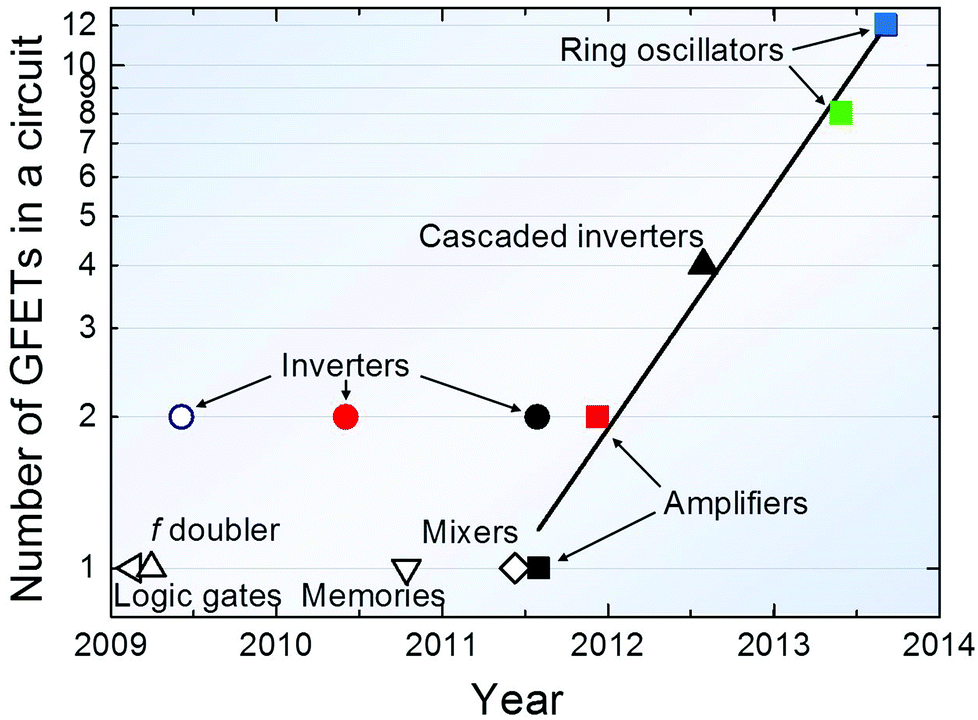 | ||
Fig. 58 Transistor count in graphene circuits with Av < 1 (open symbols) and Av > 1 (filled symbols). The linear fit is performed only on circuits with over-unity RT AC Av. From this, a graphene Moore's law is obtained: the number of GFETs on a chip currently doubles approximately every 8 months. However, it is unlikely that this will hold in the near future. Values taken from:  ,1149 ,1149 ,1150 ,1150 ,1140 ◊,11 ,1140 ◊,11 ,1143 ■,1142 ,1143 ■,1142 ,1151 ●,1141 ,1151 ●,1141 ,1129 ▲,1144 ,1129 ▲,1144 ,1155 ,1155 .1102 Adapted from ref. 1208. .1102 Adapted from ref. 1208. | ||
The first attempt to increase the transistor count was the realization of graphene complementary inverters comprised of two GFETs.1151 This was the first time a complete functionality was integrated on a single MC graphene flake, and no additional components were required. This integrated circuit also established a simple concept of complementary operation between the Dirac points of the two GFETs connected in series. However, these inverters were also back-gated, therefore exhibited Av < 1. The concept of complementary operation was later extended to top-gated inverters, exhibiting Av > 1 at cryogenic1129 and RT.1143 However, their transistor count was also 2, and there was no attempt to demonstrate multi-stage circuits, probably because of the use of MC graphene.
The first graphene multi-stage circuit comprised two inverters connected in series, thus bringing the transistor count to 4.1144 Signal matching and cascading was demonstrated under ambient conditions, with inverters fabricated from CVD graphene.1144 A good Av ∼ 5, crucial in achieving cascaded operation,1144 was obtained due to a combination of factors including full-channel gating, thin (∼4 nm) gate oxide (leading to good control of the top-gate over the channel), μ ∼ 500 cm2 V−1 s−1, low output conductance (gd ∼ 50 μS μm−1), and manageable contact resistivity (∼9 kΩ·μm). Although these inverters pave the way to realistic multi-stage circuits, they have large parasitics, limiting the clock rate to 200 kHz.1144
Multi-stage circuits must operate at high (>1 GHz) technologically-relevant frequencies to be useful. High-frequency graphene circuits were developed over the past few years, but they are all single-transistor and single-stage circuits.1153,1154 The first wafer-scale graphene integrated circuit was a 10 GHz frequency mixer, but it consisted of a single GFET integrated with two inductors.11 Similarly, high-frequency graphene voltage amplifiers were reported with Av > 1, up to 6 GHz, but with a single GFET connected to two off-chip bias tees.1142
Elimination of parasitics in inverters integrated on wafer-scale graphene paves the way to high-frequency multi-stage integrated circuits. Ref. 1102 demonstrated high-frequency GROs, consisting of 4 cascaded stages and 8 GFETs. GROs were also realized with 12 GFETs,1155 however running below 50 MHz.
GFETs must satisfy two additional requirements in order to be considered as building blocks of future logic gates: Av > 10 and ION/IOFF > 104. The short-term goal is thus to achieve Av sufficient for realistic applications where high-speed operation is desired, but power dissipation is not a concern, similar to the SiGe and InP emitter-coupled logic (ECL), the fastest logic family.1161 The long-term goal should be based on both requirements, as only in this way graphene could be considered as a replacement for Si CMOS in future ubiquitous logic gates (e.g., in microprocessors). This is not a far-fetched goal because the Si CMOS is also experiencing some fundamental difficulties related to short-channel effects, gate oxide thickness scaling, and channel carrier mobility.12,1162 As a consequence, static (leakage) power exceeds dynamic (switching) power in most state-of-the-art Si logic circuits.12,1163
In order to achieve the short-term goal it will be necessary to realize top-gated GFETs with ultra-thin (<4 nm) high- gate insulators, as Av > 1 has already been demonstrated in graphene devices with similar gate thicknesses (∼4 nm).1141–1143 The voltage gain could further be improved by using BLG. In turbostratic BLG misorientation electronically decouples the two SLGs.1164,1165 The bottom layer acts as a pseudosubstrate, which electrostatically screens the top layer from the substrate, thus giving enhanced μ within the top layer.1164,1165 In Bernal-stacked BLG a perpendicular electric field can open a moderate bandgap128 allowing large Av in dual-gate configurations.128 The next stage in the development of graphene logic should be incorporation of highly-efficient gate stacks in BLGFETs The final stage should be technology transfer to wafer-scale BLG. Once wafer-scale high-gain graphene logic gates become available, their application in ultra-fast logic circuitry should be investigated.
The long-term goal is more challenging, as no satisfactory solution has been found so far in order to open a bandgap in graphene without reducing μ. Bandgap engineering of graphene should be attempted by patterning into GNRs. However, state-of-the-art sub 10 nm GNRs have very low μ ∼ 200 cm2 V−1 s−1 (ref. 312) as a consequence of carrier scattering on disordered ribbon edges.312 In order to eliminate unwanted scattering, GNRs should have crystallographically smooth edges308,310,320 and be deposited on insulating substrates. This leads to an enormous fabrication challenge as GNR widths ∼1 nm are required in order to reach the bandgap of Si (∼1 eV), as necessary for reliable switching. GNRs, ∼40 nm wide, grown on SiC have shown huge μ (∼6 × 106 cm2 V−1 s−1) and could be a viable strategy, although the width (∼40 nm) and the SiC cost could be an issue for scaling up.100 Finally, complementary logic (Fig. 59) is currently realized through electrostatic doping1144 which imposes limits on supply voltages in logic gates. In order to lift this restriction, GNRs should be chemically doped1150,1166,1167 but this doping should not introduce additional scattering centres in order to maintain high-μ of crystallographically smooth GNRs.
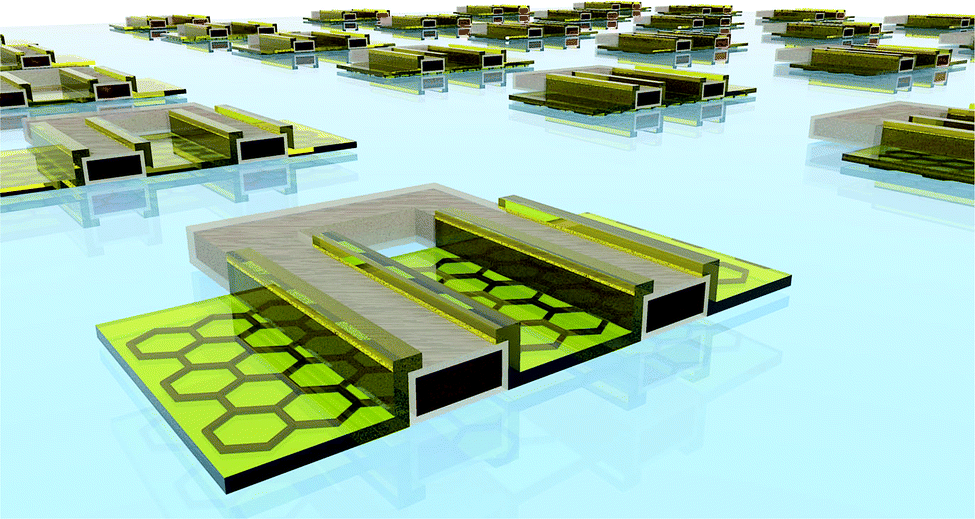 | ||
| Fig. 59 Schematic of a large array of digital complementary inverters integrated on wafer-scale graphene. Each inverter consists of two FETs that share the same gate (input) and drain (output). The gate stack is comprised of metal (Al; dark red core) covered by an insulating layer (AlOx; gray shell). Source and drain contacts (Ti/Au; yellow) overlap with gate contacts to eliminate access resistances and increase voltage gain of the inverters. | ||
Conventional GFETs cannot be turned off in either of the two logic states and a typical in/out voltage swing is 22% of the supply voltage at RT.1144 Although this is less than the voltage swing in Si CMOS (capable of rail-to-rail operation, i.e. output voltage goes from ground = 0 V–GND – to supply voltage, with the voltage swing reaching almost 100% of the supply voltage),1161 it is still more than the swing in ECL gates.1168 Similar to graphene logic gates, ECL gates also comprise overdriven transistors in order to achieve ultra-fast operation.1168 For this reason a typical swing of the ECL gates is 0.8 V at a supply of 5.2 V, i.e., only 15% of the supply voltage.1161 ECL gates are at the core of the fastest SiGe and InP bipolar-CMOS (BiCMOS) or heterojunction bipolar transistor (HBT) chips and are used for digital signal processing at ultra-high frequencies (f > 100 GHz),1169 inaccessible with conventional state-of-the-art CMOS technology. They are used in high-speed integer arithmetic units,1170 static ultra-high frequency dividers,1171 high data rate (>50 Gb s−1) serial communication systems for demultiplexing (i.e. extracting the original channels on the receiver side)1172 and phase detection for clock and data signal recovery.1173 Hence graphene logic gates could find uses in applications not suitable for traditional Si logic, such as ultra-fast logic applications where power dissipation is not a concern, or transparent circuits on flexible (plastic) substrates.
GNR FETs should be considered as a replacement for Si FETs in CMOS logic once they reach sufficiently large Av and ION/IOFF, as discussed above. However, at this stage it is not clear whether this would be sufficient to migrate from Si to graphene logic. In the very optimistic scenario in which μ in GNR FETs would exceed that in Si FETs by an order of magnitude, it would still require a FET to have 100 GNRs (W = 1 nm) connected in parallel in order to reach the same current drive of a Si FET (W = 1 μm).
The timeline is shown in Fig. 61 and the main targets for digital logic gates are: 5–10 years: Ultra-fast (>100 GHz) integrated digital logic gates replacing ECL gates. 5–10 years: Simple digital logic gates on flexible or transparent substrates. 15–20 years: General-purpose low-power GNR digital logic gates replacing Si CMOS.
Aggressive scaling of CMOS technology has a negative impact on the reliability of non-volatile memories. Parasitic capacitances between the adjacent cells increase with scaling, leading to a cross-talk.1175 Diminished lateral area leads to reduced gate coupling and therefore to higher operating voltages.1176 Larger number of array cells leads to a reduced sensing current and increased access times.1177 For these reasons, alternative materials and storage concepts have been actively investigated, including implementation of graphene in non-volatile memories1140,1178–1182 see Fig. 60. Research is needed in order to assess the most important figures of merits of non-volatile memories, such as endurance (i.e. the maximum number of cycles that the memory cell can withstand) and program/erase (P/E) [a cycle comprised of writing and then erasing data in a memory cell] curves, and to correctly extrapolate the retention time (i.e. the capability to retain a programmed state over time). Similarly to logic gates, non-volatile memories also require large enough (>104) ION/IOFF for memory states to be unambiguously resolved from one another. For these reasons, the following parameters should be thoroughly investigated: P/E curves as a function of time, the available P/E window (i.e., difference in threshold voltage or current between the two logic states), the retention, and the endurance. In addition, if graphene is to be used as a conductive channel in flash FETs, bandgap engineering should be pursued, as for graphene logic gates.
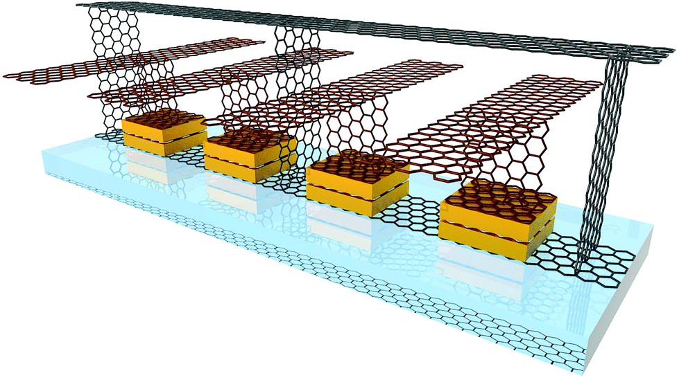 | ||
| Fig. 60 Two cells graphene NOR gate flash memory. Graphene is used for conductive FET channels1140,1181 and bit line (black), control gates1180 and word lines (brown), and floating gates1179 (white). | ||
The use of graphene in non-volatile memories is facing less challenges than in logic gates, because memory operation requires only large (>104) ION/IOFF (assuming that the on current is not too low) without need for Av > 1. Av of memory GFETs is not important, as the reliability of a memory state readout depends only on the sensitivity of the sense amplifiers connected to the bit lines. Graphene could be used in non-volatile memories as channel,1140,1181 resistive switch,1178,1182 and storage layer, i.e., replacement of floating1179 or control gates.1180
The timeline is shown in Fig. 61, and graphene non-volatile (flash) memories might be developed in 10–15 years.
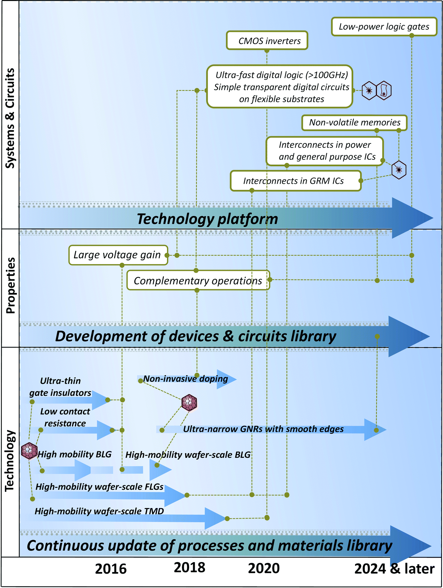 | ||
| Fig. 61 GRMs “digital electronics” timeline. | ||
Exfoliated SLG can sustain (without oxidization due to Joule heating) 1.2 mA μm−1 = 12 A cm−1 under ambient conditions.1187 Assuming that each SLG (0.33 nm) within a multilayer stack can sustain the same current density, the breakdown current density of a multilayer stack is ∼360 MA cm−2, i.e. 360 times more than Cu.1188 However, initial investigations of wafer-scale multilayer graphene stacks revealed an order of magnitude lower breakdown current density (40 MA cm−2).1189 Although this is still 40 times more than in Cu, the Rs (>500 Ω/□) of these 20 nm thick graphene stacks corresponds to σ < 0.1 × 10³ S m−1, much less than that of Cu (σ = 60 × 103 S m−1). Therefore, further development in wafer-scale graphene synthesis is needed to increase the conductivity of thick graphene films, therefore reduce parasitic resistances of graphene interconnects.
Graphene interconnects should be first introduced in ICs in which FETs are also made of graphene, in order to eliminate initial problems of contact resistance between graphene interconnects and contacts in non-graphene FETs. Eventually graphene interconnects should be introduced both in power and general-purpose ICs.
The timeline is shown in Fig. 61. 5–8 years: Interconnects in graphene ICs. 5–10 years: Interconnects in power and general-purpose ICs.
5.3. High frequency electronics
High frequency electronics is a cornerstone of today's high-tech economy. The continuous downsizing of components in ICT sustained the electronics industry for more than three decades. This field was first dominated by defence applications, until the late 1980s, and then it moved into the mainstream in the 1990s owing to advances in wireless communications.1190 Not only because miniaturization reaches fundamental physical limits, not solvable with conventional Si technology, but also because emerging applications, such as THz-spectroscopy,1191 require higher and higher frequencies, hardly achievable with established technology platforms.Thus, a radical new approach is needed. Graphene as material platform for both digital and analogue electronics might overcome many obstacles: scaling beyond the Si limits is possible because graphene is ultimately thin and the high μ allows transistors to operate at frequencies beyond 1 THz.
The first entry points in electronics industry for graphene may be in analogue high frequency electronics, as there the advantages are most distinct in comparison with established technologies. Graphene may allow higher operation frequencies for frequency doubling and mixer applications than Si or Si/Ge, avoiding disadvantages of III/V materials, such as production costs, toxicity and poor integrability into a cost efficient Si technology.
In addition, ambipolar devices can significantly reduce the number of transistors needed in these applications. Simpler circuits mean less power consumption and smaller chip area. Considering that RF circuits are much less complex than digital logic ones, makers of RF chips are more open to new device concepts. Indeed, a large variety of different transistor and materials are today used in RF electronics, such as Si n-channel MOSFETs, HEMTs based on III–V semiconductors (GaAs;InP), and various bipolar transistors.1192
Graphene transistors with a 240 nm gate length operating at frequencies up to 100 GHz were demonstrated in early 2010.788 This cut-off frequency is already higher than those achieved with the best Si MOSFET having similar gate lengths.788,433 Cut-off frequencies over 300 GHz were reported with graphene transistors with a 140 nm gate length, comparable with the very top HEMTs transistors with similar gate lengths.1197 More recently, a cut-off frequency of 427 GHz was extracted for a 67 nm channel length graphene transistor,1198 see Fig. 62. These results are impressive, comparing the young age of graphene with the longer timescales of other devices. This is also a clear indication that GFETs have the potential to pass the THz-border in the near future. Thus, graphene may offer a cost efficient platform for novel applications in a variety of fields, such spectroscopy or automotive radar in analogue high frequency electronics. Significant impact in analogue RF communication electronics in areas as diverse as low noise amplifiers, frequency multipliers, mixers and oscillators could be achieved within the next 10 years, see the timeline in Fig. 67.
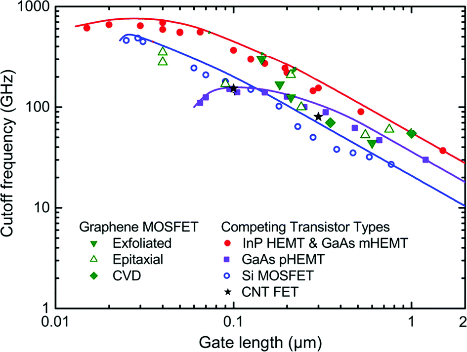 | ||
| Fig. 62 Cut-off frequency versus gate length for GFETs, nanotube FETs and three types of RF-FETs [Adapted from ref. 1193]. pHEMT = pseudomorphic HEMT, mHEMT = metamorphic HEMT. HEMTs are made of heterojunctions, i.e., junctions of different materials.1194,1195 The most common example are GaAs HEMTs in which there are junctions between AlxGa(1−x)As and GaAs. Different materials have different lattice constants, hence crystal defects are expected in HEMTs. In pHEMTs this is avoided by using a very thin layer of one material1196 so that accumulated energy in this layer is not enough to relax the layer and introduce defects (energy is low because the layer is very thin).1196 In mHEMTs a graded buffer layer is used in between the layers to accommodate both lattice constants1196 and eliminate the defects. E.g., to grow Al0.3Ga0.7As on GaAs, an AlxGa(1−x)As layer is grown first in which x = 0 at the beginning (GaAs) and then x is gradually increased to 0.3 (Al0.3Ga0.7As).1196 | ||
Research efforts will not only be required for the optimization of graphene-based devices, but also for the development of circuit designs that can fully exploit the unique properties of graphene-based devices. The absence of a band-gap, therewith the un-incisive current saturation, the ambipolarity and the targeted operation frequencies going beyond 100 GHz require new concepts on system level and circuit design, which could also open the door towards novel functionalities. Thus, to take advantage of the full potential of graphene devices, the aim is to combine more basic research with improved material growth and device technology. A better understanding of parameters such as breakdown voltage, electron velocity, and saturation current is needed to allow a complete benchmark of this material and an evaluation of its potential performance. In addition, these new applications will have to overcome the limitations that arise from the lack of band-gap.
Once the growth and fabrication technology matures, the main challenges for RF applications are the integration of graphene devices in Si technology, and the increase of their trans-conductance by, e.g., introducing a band gap, and ensuring sufficient Av and output currents so that components can be integrated to circuits.
For real applications not only the cut-off frequency is an important figure of merit; Av and fmax, the frequency where the unilateral power gain reaches unity, are even more important. Both of these quantities are much more sensitive on the process technology than the cut-off frequency. In graphene transistors Av and fmax still lag behind established technologies. Therefore, much effort on developing the process technology is required. Additionally, integrated circuits of higher complexity have not been realized so far, because the required process technology is still in its embryonic stage and circuits can hardly be designed, as a parameter library for graphene-based devices is still missing.
Advanced graphene devices have the potential to transform communication systems in a broad array of new applications in the next 20 years. Graphene is therefore in an excellent position to help RF systems become even more ubiquitous and versatile than they are today.
One of the main factors contributing to a low Av is the use of back-gated Si/SiO2 devices, which also suffer from large parasitic capacitances and cannot be integrated with other components. For this reason, top-gated GFETs with thinner gate insulators were extensively investigated,1201 as in case of digital logic gates.
The future investigation of graphene voltage amplifiers partly overlaps with that of digital logic gates, as in both cases the short-term goal is the same: large Av > 10 should be obtained in wafer-scale SLG and BLG grown by CVD or on SiC substrates. In order to further increase Av, FETs should be fabricated from wafer-scale BLGs. Finally, several remaining challenges of GFETs, technological rather than fundamental in nature, should be addressed. E.g., graphene circuits remain sensitive to fabrication induced variability. Higher μ, gm and lower gd and contact resistance should increase Av for both analogue and digital applications. The long-term goal should be the integration of graphene amplifiers in more complex (i.e., multi-stage) analogue circuits.
GFETs are well suited as building blocks of low-noise amplifiers (LNAs) as they exhibit very low levels of electronic flicker noise102 (or 1/f noise, where f is the frequency, occurring in almost all electronic devices and related to a direct current: a resistance fluctuation, which is transformed to voltage or current fluctuations via Ohm's law) which dominates the noise spectrum at low frequencies.1202–1204 Such voltage amplifiers are also expected to benefit from graphene's high mechanical and chemical stability and high κ.102 Graphene LNAs are needed in high-frequency electronics,1205,1206 as their realization would allow seamless integration with graphene analogue mixers, thus eliminating need for Si FETs in these applications. As present, GFETs cannot be turned off, thus class-A amplifiers (i.e. amplifiers which conduct during the whole input cycle) with low harmonic distortions should be developed. Large Av may allow realization of electronic harmonic oscillators, combining high-Av amplifiers with passive graphene feedback networks.
The development of graphene voltage amplifiers could pave the way for graphene power amplifiers. These are usually found in the final stages of more complex amplifiers. They operate with Av = 1 and have a sole purpose to match the previously amplified signals (provided by the voltage amplifiers) to a low-impedance load, such as a loudspeaker (∼4 Ω) in high-fidelity audio systems1207 or antenna of a transmitter (∼50 Ω) in RF applications.
The timeline is shown in Fig. 67. 3–4 years: LNAs. 4–5 years: Audio and RF voltage amplifiers. 5–6 years: Harmonic oscillators. 5–10 years: Power amplifiers.
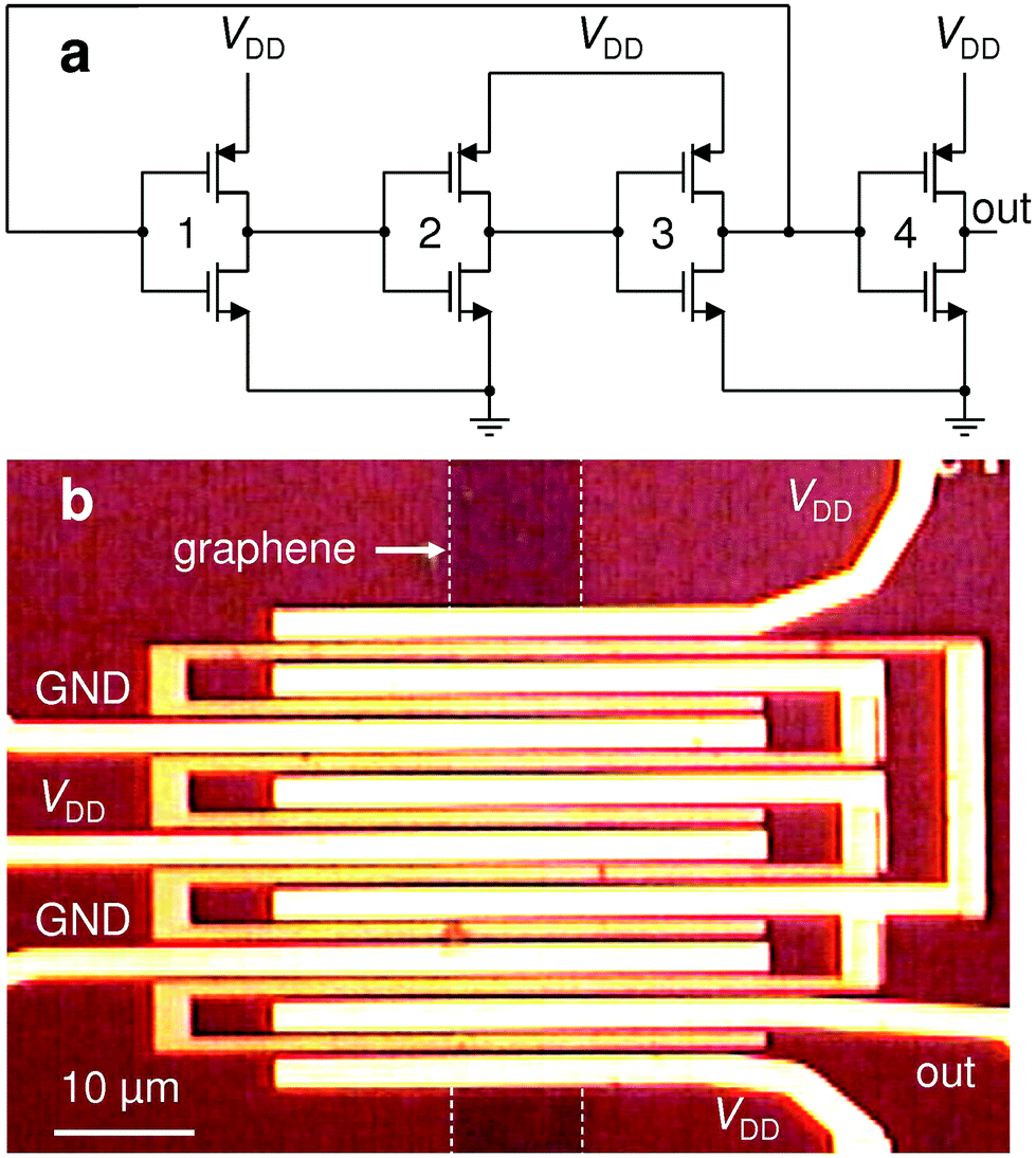 | ||
| Fig. 63 Integrated GRO. (a) Circuit diagram of a three-stage RO. The RO comprises three inverters (1–3) cascaded in a loop with a fourth inverter (4) decoupling the RO from the measurement equipment connected to the output (out). (b) Optical microscope image of a RO with gate length L = 1 μm integrated on a CVD graphene channel. The drain contacts of inverters 1–3 (Au) overlap with the gate contacts (Al/Ti/Au) in order to form internal connections between the inverters. GND = ground. Adapted from ref. 1102. | ||
Complementary operation of the inverters within a RO was obtained between the Dirac points of two GFETs1102, as in early graphene inverters.1149 These inverters have Av > 4, enough to enable oscillations under signal matching. The oscillation frequency of a RO with n stages cascaded in a loop is inversely proportional to the inverter rise/fall delays τ as fo = 1/(2nτ) = fo1,1210 where fo1 is a fan-out of one (FO1) oscillation frequency, where fan-out is the number of digital inputs that the output of a single logic gate can feed. Since τ ∼ CGD−1,1102 with GD the sum of extrinsic drain conductances of the GFETs in the inverter and C the parasitic capacitive load of the inverter, reduction of parasitics leads to high-frequency operation.
The speed of electronic circuits is typically increased by downscaling their dimensions,12 which also reduces parasitics (because parasitic capacitances are proportional to the surface area of the corresponding device parts). This is demonstrated in Fig. 64, plotting the maximum oscillation frequency of 26 GROs as a function of gate length L. The highest is fo = 1.28 GHz at L = 1 μm, corresponding to a FO1 τ ∼ 100 ps. This is similar to that of conventional Si CMOS ROs,1211 and smaller than polycrystalline Si CMOS thin-film ROs1212 for the same L. This is the first operating frequency above 1 GHz in digital circuits based on any type of novel low-dimensional materials (e.g. nanotubes, nanowires, graphene, MoS2). By comparison, the highest frequency of nanotube ROs was ∼50 MHz,1213 and 1.6 MHz in 2L-MoS2 ROs.1214
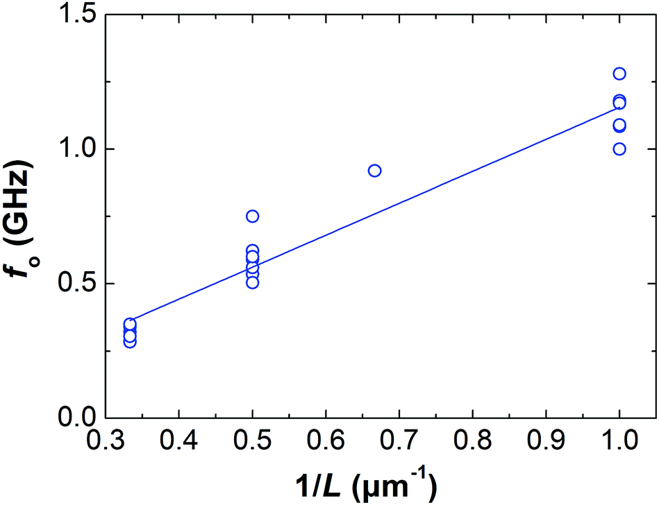 | ||
| Fig. 64 Scaling of oscillation frequency with L−1. The plot shows the values from measurements on 26 GROs (only the highest frequencies for each GRO are shown).1102 | ||
The dependence of the oscillation frequency of conventional ROs on the supply voltage is a serious problem in complex digital circuits, since increased power consumption places strong demand on the supply voltage causing it to fluctuate.1215 Such fluctuations degrade the operation of logic gates and their noise performance.1215 In contrast to other types of ROs, GROs are much less sensitive to fluctuations in the supply voltage, as a consequence of their reduced voltage swing.1102 Insensitivity to power supply noise could be a disadvantage in applications in which dynamic frequency and voltage scaling are used to slow the clock rate of digital circuits during periods of reduced workload. However, such insensitivity represents an important advantage in applications in which frequency stability is important, e.g. for clock generation and recovery in high-speed digital systems.
GROs and inverters could find applications in digital circuits operating at extremely high frequency (EHF; f > 100 GHz) in which high operating speed could be traded off against power dissipation, reduced voltage swing, and circuit complexity1170,1172,1173,1216 These ultra-high speed digital circuits were developed to perform data conversion at the transmitting/receiving side of serial EHF lines,1217 such that information carried by EHF digital signals can be processed at lower clock rates by low-power, highly integrated, and parallel Si CMOS logic.1217 The EHF digital circuits are used in wireless, fiber-optic, and space communications.1169
GROs can find applications in analog electronics. Oscillators are one of the main building blocks of analog electronics,1218e.g. RF (microwave) electronics is built on voltage amplifiers, oscillators, and mixers.1219 Graphene amplifiers,1142,1143 mixers11,1220 and oscillators1102 may allow realization of all-graphene microwave circuits.
GROs can also be used to mix analog signals. Graphene analog mixers11,1220 so far require an external local oscillator (LO) for frequency conversion.11,1220 GROs can overcome this limitation and perform both modulation and generation of oscillating signals to form stand-alone graphene mixers, i.e. mixers with a built-in LO. To this end, the GRO in Fig. 63 was modified by superimposing a RF signal over the DC supply of the buffering inverter 4 (without affecting the supplies of the other three inverters).1102 As the other inverters forming a ring are not affected by the addition of the RF signal, the buffering inverter mixes the RF signal with the unaltered AC component of the oscillating voltage. Fig. 65 shows the power spectrum of the up-converted RF signal around the LO signal. The conversion loss is 19.6 dB at an LO power of −18.5 dB m and RF power of −34.3 dB m, better than in early graphene mixers,11,1220 and comparable to recent graphene mixers.1221,1222
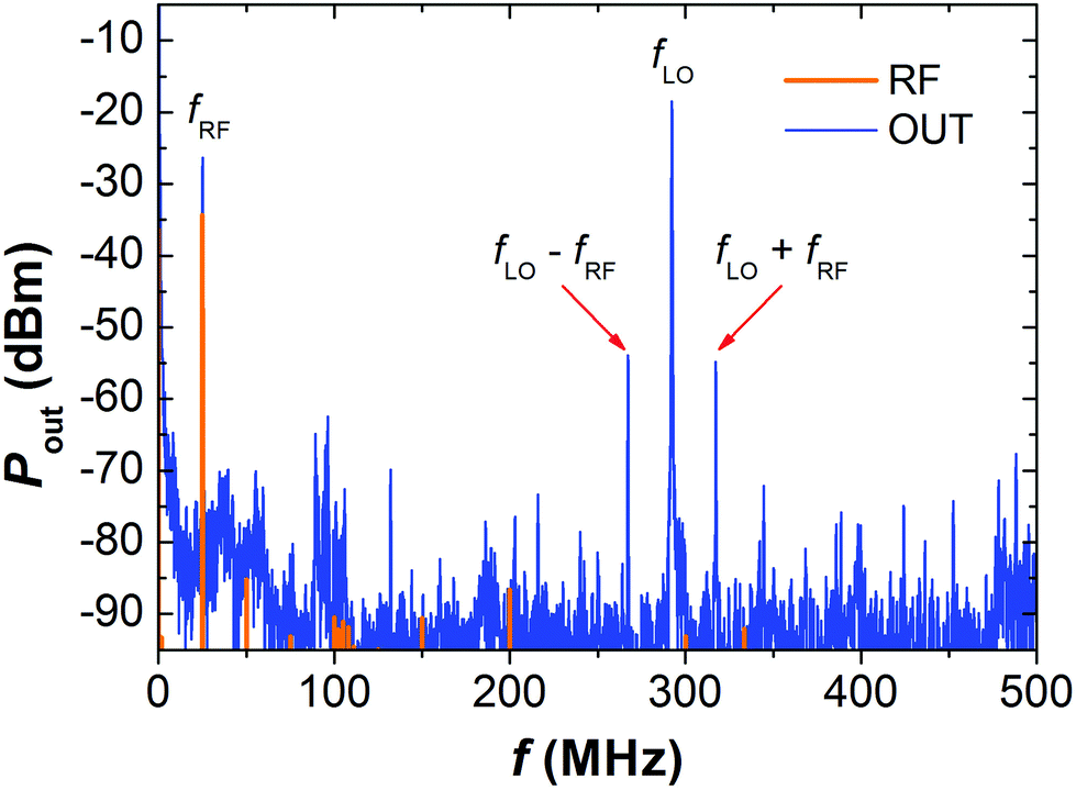 | ||
| Fig. 65 Power spectrum of the output signal of a stand-alone graphene mixer at VDD = 2.5 V. The signal frequencies are fLO = 292 MHz and fRF = 25 MHz. Apart from the signals discussed in the text, the output signal also contains a frequency component at fRF, from the amplification of the RF signal by inverter 4 in Fig. 63.1102 | ||
5.4. Layered materials-based devices
From the device point of view, bulk MoS2 seems to be a most interesting LM because its monolayer is a direct bandgap (1.8 eV) semiconductor,111 which allows realization of electronic379 and optoelectronic378,1223 devices. Due to a large band gap, FETs fabricated from 1L-MoS2 exhibit large ION/IOFF ∼ 108.379 The current μ in 1L-MoS2 deposited on conventional insulating substrates (e.g., SiO2) is high enough5,384,1231 for electronic applications at technologically relevant frequencies (>1 GHz).2338 The low current drive of MoS2 FETs can be improved by using 2L-MoS2 at the expense of a small reduction of ION/IOFF (∼107).1214 In this case, the highest oscillation frequency in 2L-MoS2 ROs is 1.6 MHz, limited by the high gate capacitance.1214μ of MoS2 was increased up to ∼500 cm2 V−1 s−1 in thicker layers (∼50 nm) deposited on PMMA.1224 However, such samples suffer from even smaller ION/IOFF (∼104) and are yet to be incorporated in top-gated FETs.Theoretical predictions show that at RT, μ is expected to be limited by phonon scattering,1225 with values in the 320–410 cm2 V−1 s−1 range,1225 so further improvements in material and device processing seem possible. Provided that the charged impurity concentration could be sufficiently reduced, at low T μ would be dominated by scattering by acoustic phonons,1226 and μ > 105 cm2 V−1 s−1 for T < 10 K and carrier concentration >1011 cm−2 was predicted in ref. 1226. Other possible sources of scattering are ripples that have been observed in MoS2 membranes.1227 These consist of local height fluctuations and are also expected to reduce the conductivity of 1L-MoS2.1228
1L-MoS2 devices exhibit n-type transport behaviour. Ambipolar transport was demonstrated in thin (10 nm) MoS2 electrical double-layer transistor using an ionic liquid as the gate.1229 The demonstration of both p and n-type transport in devices based on solid-state dielectrics would be useful for applications in CMOS-type logic and pn-junctions for optoelectronic devices. The use of liquid gates has also recently allowed large charge carrier concentrations in 10 nm thick MoS2 and gate-tunable superconductivity.1230 Metal-insulator transition in 1L-MoS2 Hall-bars using classical dielectrics (HfO2) was reported.1231
The presence of a band gap in MoS2 allows strong drain current saturation, with drain-source conductance gds = dIds/dVds < 2 μS μm−1 demonstrated in 1L-MoS2,1232 together with high transconductance gm of 34 μS μm−1, which should allow high voltage gains for small signals (AV = gm/gds > 10). Such gains allowed the fabrication of digital circuits based on MoS2, such as inverters,1044 ROs1214 as well as analogue amplifiers.1233
Transistors based on MoS2 can also operate with current densities of at least 4.9 × 10⁷ A cm−2,1232 50 times higher than Cu, comparing favourably to the breakdown current density for graphene on SiO2 (>108 A cm−2).103 This is due to intralayer Mo–S covalent bonds being much stronger than metallic bonds. Such high breakdown current density would allow aggressive downscaling of MoS2 devices. Integration with high κ substrates, such as diamond,199 could result in further increase of breakdown current density.
Device simulations of 1L-MoS2 transistors425,1234 predict that 1L-MoS2 would show superior resistance to short-channel effects due to its small thickness. These calculations show that top-gated MoS2 transistors with gate lengths of 15 nm could operate in the ballistic regime with on-current as high as 1.6 mA μm−1, subthreshold swing close to 60 mV dec−1 and ION/IOFF ∼ 1010. Although MoS2 will probably not compete with conventional III–V transistors on μ values, attractive electrical performance characteristics and high electrostatic control could make it and other TMDs viable candidates for applications in low-power electronics.
The use of 2d materials could be very advantageous for the realization of memory devices based on the floating gate transistor structure,1235,1236 used in flash memories. In this type of device, the operation is based on detecting a threshold voltage shift caused by a presence or absence of charges trapped on the floating gate. Decreasing the device size is limited by the amount of charge that can be stored on the floating gate. Using 1L-MoS2 or other 2d semiconductors as conductive channels in such devices brings the benefit of increased sensitivity to external electric charge and could allow deeper scaling. Such devices based on 1L-MoS2 and graphene as key elements were reported1235 in a geometry shown on Fig. 66. Graphene here acts as an ohmic-like contact, allowing efficient charge carrier injection into MoS2 while multilayer graphene is used as the floating gate. The use of a 2d contact in place of thicker metallic films is beneficial for several reasons. It allows one to realize devices and circuits with 2d materials using less expensive fabrication techniques, e.g. R2R printing, see section 4.11.8.
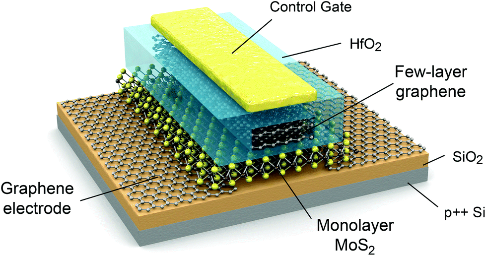 | ||
| Fig. 66 MoS2/graphene heterostructure memory layout. 3d schematic view of the memory device based on 1L-MoS2 semiconducting channel, SLG contacts and FLG floating gate. The FLG floating gate is separated from the channel by a thin tunnelling oxide and from the control gate by a thicker blocking oxide. | ||
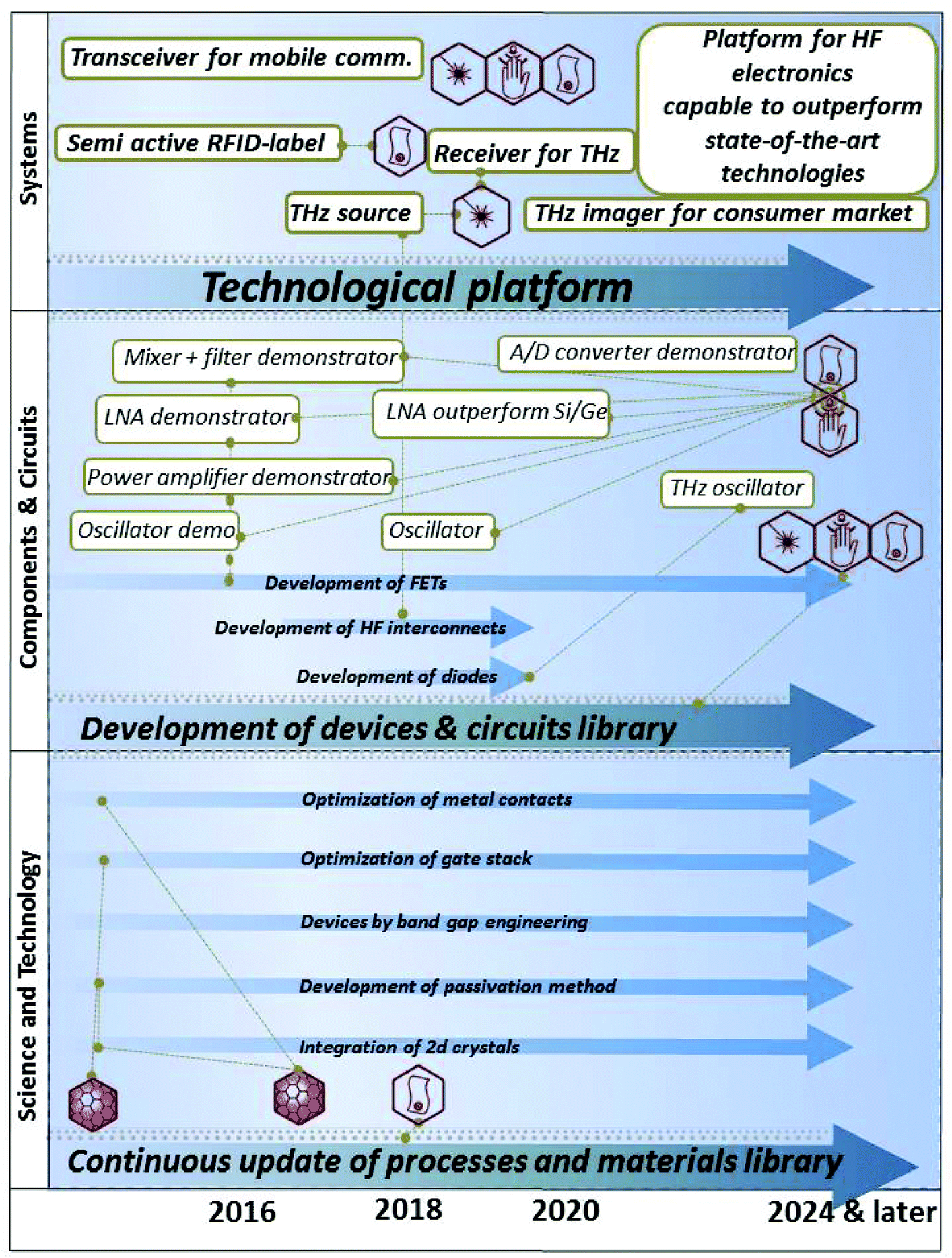 | ||
| Fig. 67 High frequency electronics timeline. | ||
The capacitive coupling between leads in neighbouring devices is also reduced, allowing further scaling. Because of its band gap and 2d nature, 1L-MoS2 is highly sensitive to the presence of charges in the charge trapping layer, resulting in a factor of 104 difference between memory program and erase states.1235 This allows a large memory window and the possibility to have different intermediate levels of charge in the floating gate corresponding to multiple bits of information.
Several issues however still need to be addressed. There is at this point no control over intrinsic doping in MoS2 and methods for introducing dopant atoms as well as achieving ambipolar and p-type behaviour would be highly desirable. Understanding how to make good electrical contacts to MoS2 is also lagging and it is not clear yet which material and contacting scheme would result in the smallest possible contact resistance.
Few-layer phosphorene116,1237 has been investigated as a new 2d p-type electronic material. Few-layer phosphorene is stable, having a direct band-gap that depends on the number of layers,116 going from ∼2 eV in monolayer to ∼0.3 eV in bulk.1237 Phosphorene field-effect transistors with 1 μm channel length have shown a RT μ (hole) ∼ 286 cm2 V−1 s−1, and ION/IOFF up to 104.116Ref. 1237 reported that μ in few-layer phosphorene is thickness-dependent, with the highest achieved values of ∼1000 cm2 V−1 s−1 obtained for ∼10 nm samples at RT. Although these results116,1237 demonstrate the potential of few-layer phosphorene as a new 2d material for applications in nanoelectronic devices, these are only the first reports and more work is needed to fully assess this material.
5.5. Novel vertical and planar transistors and devices
2d heterostructures offer richer opportunities in terms of physics and transport properties than each of the individual 2d crystals. The most obvious device to develop is the TFET.106 Initial results indicate that such devices will indeed offer required parameters in terms of ION/IOFF and μ. Other directions to explore, both experimentally and theoretically, are hot electrons transistors, resonant tunnelling and formation of minibands.Planar devices can include double quantum wells, drag in parallel 2d electron gases, Bose–Einstein condensation in such systems, etc. Also, effects of enhancement of electronic properties (improved μ) for each individual conductive layer need to be addressed.
Exotic combinations, such as superconductor/insulator/normal metal or superconductor/insulator/ferromagnet, or even more complex structures, providing one can find suitable 2d crystals, need investigation. Such devices would allow the exploration of quasi-particles spin and valley degrees of freedom. By embedding nanoclusters of conventional metals, ferromagnets, and semiconductors between the layers, it may be possible to combine the opportunities for quantum technologies offered by the QD physics and the unique electronic properties of 2d heterostructures.
The aim is to explore, by experiments and modelling, several architectures for tunnelling/hot electron transistors. The simplest is metal/BN/SLG/BN/SLG, where the metal contact (separated from the bottom graphene by thick, tunnelling non-transparent BN) serves as a gate and the two graphene layers (acting as emitter and collector) are separated by thin BN layers, Fig. 68. This relies on voltage tunability of the tunnelling density of states in graphene, and on the effective height of the tunnel barrier adjacent to the graphene electrode.
 | ||
| Fig. 68 BN/SLG/BN/SLG/BN devices.106 (A) Optical image. (B) Electron micrograph. Two 10-terminal graphene Hall bars are shown in green and orange. The scale is given by the 2 μm Hall bar width. | ||
Configurations with several different dielectrics and the use of other heterostructures, such as metal/BN/SLG/MoS2/SLG, will need investigation. Proof of principle devices with BN tunnelling barriers were demonstrated with RT ION/IOFF ∼ 50.106 With an improvement of the quality of the heterostructures and the use of dielectrics with thinner tunnelling barriers, ION/IOFF may be brought close to that required by modern electronics (105). Ref. 1238 reported a graphene-WS2 heterotransistor with ION/IOFF > 106.
The investigation, by experiments and modelling, of other possible geometries for vertical transistors, including hot electron transistors similar to ref. 443, will need to be carried out. Few-atom-thick transistors1238 based on a 2d tunnel barrier and graphene may allow much better quality, and become more successful in applications.
The transit time through such sandwiches is expected to be ≪1 ps, whereas there are no limits for scaling down in the lateral direction to true nm sizes. Metal/BN/SLG/BN/SLG structures with both BN barriers transparent for tunnelling, and bottom graphene as the control electrode, can be exploited. The thickness of the active part would be <10 atoms (∼3 nm) and should allow ballistic current that is controlled by the central graphene electrode.
Attempts to produce stacks of several transistors in series (metal/BN/SLG/BN/SLG)N, thus introducing a vertical integrated circuit architecture, need to be carried out. Other possible architectures and electronic components as well as different ways of integration into vertical integrated circuits should be studied. E.g., a gate-tunable p–n heterojunction diode using s-SWNTs and 1L-MoS2 as p-type and n-type semiconductors, respectively, has been demonstrated.1239 The vertical stacking of these two direct band gap semiconductors forms a heterojunction with electrical characteristics that can be tuned with an applied gate bias to achieve a wide range of charge transport behavior ranging from insulating to rectifying with forward-to-reverse bias current ratios exceeding 104.1239
It will be necessary to investigate integration of tunnelling devices in realistic circuits, which require much larger on currents than currently obtained. Large on currents are needed in order reach AV > 1. In addition, in order to fully exploit the short intrinsic transition time of tunnelling devices, large on currents (i.e., small on resistances) are needed to reduce extrinsic RC time constants associated with capacitances in electronic circuits.
The advent of SLG/h-BN and other heterostructures offers a new venue for investigation of interlayer interactions. First, the 2d charge carriers in graphene are confined within a single atomic plane, whereas a few atomic layers of h-BN are sufficient to isolate graphene electrically. This allows extremely small (nm) separation between the graphene layers, which favourably compares with the smallest effective separation ∼15 nm achieved in GaAlAs heterostructures.1241 Second, charge carriers in graphene can be continuously tuned between e and h from n > 1012 cm−2 all the way through the neutral state, where the inter-particle distance nominally diverges.1241 This makes it possible to access the limit of strongly interacting 2d systems. First results demonstrate very strong Coulomb drag in BN/SLG/BN/SLG/BN systems,106 see Fig. 69. Optimisation of the structures may lead to many interesting effects.
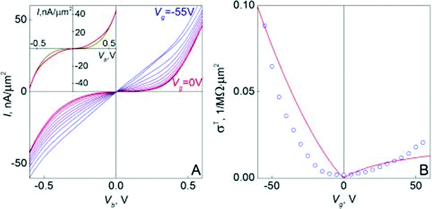 | ||
| Fig. 69 (A) Tunnelling I–V s and their response to gate voltage (in 5 V steps) for a BN/SLG/(BN)4/SLG/BN device.106T = 300 K. (B) Changes in low-bias tunnelling (symbols) and the theory fit for 4 hBN layers (solid curve). Adapted from ref. 106. | ||
On the theory side, there is need to impose rigor onto widely varying conflicting predictions for the Coulomb drag and a related issue of exciton condensation.24Ref. 432 exploiting heterostructures comprising a SLG (or BLG) carrying a fluid of massless (massive) chiral carriers,1078 and a quantum well created in GaAs 31.5 nm below the surface, supporting a high-mobility 2d electron gas, found that the Coulomb drag resistivity significantly increases for T below 5–10 K, following a logarithmic law.432 This anomalous behavior is a signature of the onset of strong inter-layer correlations, compatible with the formation of a condensate of permanent excitons.432
Additionally, there is the need to evaluate the contribution of the phonon drag, related to the emission/absorption of vibrations in the separating insulating layers.
The opportunity to generate new or to enhance the earlier discussed correlation effects in structures with a complex architecture should be explored. The formation of an excitonic insulator in the BLG systems is hindered by screening of the Coulomb interaction, which appears to be sensitive to the electron spin and valley degeneracy. The T of the excitonic insulator transition in MoS2/(BN)n/MoS2 sandwiches may be higher and fall into the experimentally accessible range. Also, the search for correlated states in NbSe2/(BN)n/NbSe2 sandwiches should be undertaken, since these, by extrapolating from bulk properties of NbSe2 (ref. 1242), may form both charge density waves and superconductivity.
5.6. Electron emission
“Vacuum microelectronics” has been of interest since the 1970s.1243,1244 Its development was initially driven by the aspiration to create new, more efficient, forms of electronic information display known as “field effect (FE) displays”1245 or “nano-emissive displays”.1245 Even though prototypes have been demonstrated,1245 the development of such displays into reliable commercial products has been hindered by a variety of industrial production problems, essentially related to individually addressable sub-pixels technology, not directly related to the source characteristics. However, after considerable time and effort, many companies are now shutting down their effort to develop this technology commercially. This is essentially connected with the huge development of both flat-panel liquid crystal and organic light emitting diode (OLED) displays. Nevertheless, in January 2010, AU Optronics acquired FE display assets from Sony continuing the development of this technology.1246 Large-area FE sources involve many other applications, ranging from microwave and X-ray generation, space-vehicle neutralization and multiple e-beam lithography to plastic electronics.The early devices were essentially the “Spindt array”,1243 and the “Latham emitter”.1247 The first used Si-integrated-circuit fabrication techniques to create regular arrays where Mo cones were deposited in cylindrical voids in an oxide film, with the void covered by a counter-electrode (CE) with a central circular aperture. In order to avoid IC fabrication the Latham emitters were developed.1247 These comprise two different devices, the metal–insulator–metal–insulator–vacuum and the conductor–dielectric–conductor–dielectric–vacuum.1247 The latter contained conducting particulates in a dielectric film and the FE is assured by the field-enhancing properties of the micro/nanostructures.
Nowadays this research area targets the development/investigation of new nanomaterials that could be grown/deposited on suitable substrate as thin films with appropriate FE properties. In a parallel-plate arrangement, the field between the plates (FM) is given by FM = V/W, where V is the applied voltage and W is the plate distance. If a sharp object is grown/deposited on one plate, then the local field F at its apex is greater than FM and can be related to FM by: F = ζFM. The parameter ζ is called the “field enhancement factor” and is essentially determined by the object's shape.1248 Because FE characteristics are determined by F, the higher ζ, the lower FM and, for a given W, the lower V at which field emission occurs.
FE from amorphous, “diamond-like” carbon1249,1250 and nanostructured carbon films1251,1252 has been investigated for decades. The introduction of CNT-FEs,1253–1256 was a significant step forward, with extensive research carried out both for their physical characteristics and possible technological applications.1253–1256 In recent years there has also been interest in the development of nanostructures, with a sufficiently high density of individual emission sites based on other carbon forms such as “carbon nanowalls”1257 and on various forms of wide-band-gap semiconductor.1258
Graphene has atomic thickness, high aspect ratio (ratio of lateral size to thickness), excellent σ, and good mechanical properties, which qualify it as an attractive candidate as FE source.1259–1262 Carbon has one of the lowest sputter coefficients,1263 which is an advantage as an electron source is usually bombarded by positive ions. Consequently, thanks to the aforementioned properties, an enhanced local electric field and good electron-emission stability can be expected for graphene (Fig. 70).
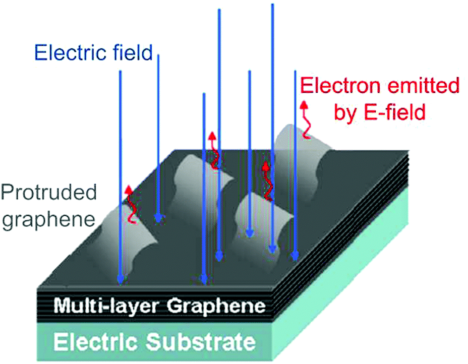 | ||
| Fig. 70 Screen-printed graphene FE device. | ||
The presence of edges may render graphene superior to CNTs for tunnelling of electrons.1260 Indeed, the atoms at graphene edges can have an unconventional electronic structure1264 and may form a distorted sp3-hybridized geometry,1260 instead of a planar sp2-hybridized configuration, with the formation of localized states, with possible barrier decrease for electron emission.1260 The orientation of graphene deposited on the substrate is another key factor for high rate FE. Indeed, graphene sheets deposited flat on the substrate surface show low field enhancement.1261 Both the interface contact and adhesion between graphene and substrate need be optimized to facilitate electron transport, and consequently improve FE performance.
The target is to position graphene as a material for vacuum nanoelectronics. One needs to develop new concept devices, to make graphene useful in applications such as lighting elements, high-brightness luminescent elements, FE lamps, cathode-ray lamps, X-ray-tube sources, electron sources for high-resolution e-beam instruments such as e-beam lithography machines and electron microscopes, EM guns and space applications, such as the high-precision thrusters needed for next generation of space telescopes. However, whichever is the application, FEs work best in UHV. The degradation of emission performance by adsorption of gas atoms needs to be addressed. This is a common problem with all FE devices,1245 particularly those that operate in “industrial vacuum conditions”.1247 The emitter shape and work function can in principle be modified deleteriously by a variety of unwanted secondary processes, such as bombardment by ions created by the impact of emitted electrons onto gas-phase atoms and/or onto the surface of CEs. Moreover, impurities such as oxygen, water, and organic residues are unavoidably absorbed on the graphene-emitter and the substrate during the transferring process to the FE chamber. The impurities could form dipoles and apply an additional disturbance on local electrical field near the graphene edge. The disturbance may change the local work function.137 In addition, a number of electrons emitted from the cathode could be trapped in the impurities in front of cathode, reducing its local electrical field. Therefore, the emission performance could be degraded. Emission stability, lifetime and failure mechanisms, energy spread, reduced brightness all need to be addressed.
The FE properties of graphene films may be further improved by optimizing the intrinsic structure of graphene, the deposition processing, and the morphology and thickness of the films. Reliable methods for the deposition of field emitting graphene and/or graphene/polymer composite films on different substrates need to be investigated and developed, opening up avenues for a variety of applications. Uniform morphology, high graphene density, and optimum graphene sheets orientation with respect to substrate surface (graphene edges normal to the substrate) may ensure emission uniformity and sufficient field-emission tips on the film surface in order to lower the threshold fields (<1 V μm−1). A successful strategy could rely on the growth of vertically aligned graphene sheets.
6. Spintronics
During the past decade, a huge research effort focused on providing new opportunities for beyond CMOS applications. It is now widely accepted that the emerging solution will be a hybrid of the most interesting technologies rather than a single one. New breakthroughs are expected at the boundary between different fields from chemistry to solid state physics, mechanics and optics, coupling their different degrees of freedom. There are increasing incentives to explore new avenues to follow the ever growing need for computational speed and storage capability. While some of the directions look at new types of devices (such as cross-nanowire transistors1265), others explore novel physical phenomena (using electron spin1266 instead of charge) and alternative materials such as graphene.Devices relying on spintronics hold unique prospects for ICT, but, to date, the advent of spintronics-based logic has been impeded by the difficulty to achieve both long spin lifetimes and spin control simultaneously. Spin control is usually associated with a sizable spin–orbit coupling.1267 However, a large spin–orbit coupling tends to lead to fast spin decoherence.1268 Novel materials and approaches to circumvent this problem are crucially needed.
In this perspective, graphene offers opportunities for efficient spin manipulation and for the creation of a full spectrum of spintronic nanodevices beyond current technologies, including ultra-low energy demand devices and circuits comprising (re-) writable microchips, transistors, logic gates, and more, while being compatible with more-than-Moore CMOS and non-volatile low energy magnetoresistive random-access memories (MRAM). Graphene provides solutions to integrate several elements (active and passive) on the same platform. While graphene- or GO- hybrids have been shown to have memory effects,1269 the underlying microscopic mechanisms still need to be clarified. Non-volatile GFETs with ferroelectric gates have been demonstrated to operate as three terminal resistive memories,1270 while graphene-based memristors (non-linear passive two-terminal electrical components)162 are interesting since they may act both as memory and logic elements.
6.1. Graphene spintronics
There are two fundamental properties of the electron which are exploited in advanced technology – charge and spin – but conventionally their functions have been kept separated.1271 The charge is used in all electronic devices, particularly in logic circuits, where current flows are controlled using electric fields, encoding and processing binary (or analogue) information. The spin is used in its “collective” form of magnetic domains for long-term data storage, from ferrite core memories to modern hard drives.1271This separation has begun to change with the advent of spintronics, a relatively young field, the name itself having been introduced only in 1996.23 This combines charge and spin of electrons in the solid state to create novel functionalities. In the simplest spintronic device, called spin-valve,1272 an electronic current flows between two ferromagnetic electrodes through a non-magnetic channel carrying a spin signal along with it, normally detected through its magnetoresistance,26 and its transport properties are influenced by magnetic ordering. The requirement for non-magnetic channels is to transport spin currents, minimizing spin relaxation due to spin-scattering events that produce spin-information losses through spin-flipping, ultimately (in most cases) caused by spin–orbit coupling.1273,1274
Graphene consists of light atoms, thus exhibits (in its pristine form) negligible spin–orbit coupling1275 and a possible absence of hyperfine interactions, due to the lack of nuclear spins in isotopically pure materials. These are the properties required for high spin-signal conservation,1276 making graphene an interesting candidate for non-magnetic channels, with long spin relaxation and coherence times, the central benchmarks for spintronic devices.
Integration between graphene and other materials, including 2d crystals, shows great potential for further improvements. This includes, e.g., substrate optimisation, as shown by the remarkable increase of spin relaxation length obtained by depositing graphene on a BN substrate1277 or on FLG.223,1278–1280 However, from Hanle experiments (i.e. magnetoresistance measurements in which the spin is forced to precess by an external magnetic field, while the magnetoresistance signal is monitored by spin diffusion length,223,1300 see Fig. 71), spin relaxation times have been reported to be in the ns range for varying quality of graphene samples,1276 whereas the spin relaxation mechanism is under debate, and a fully comprehensive picture is still lacking.
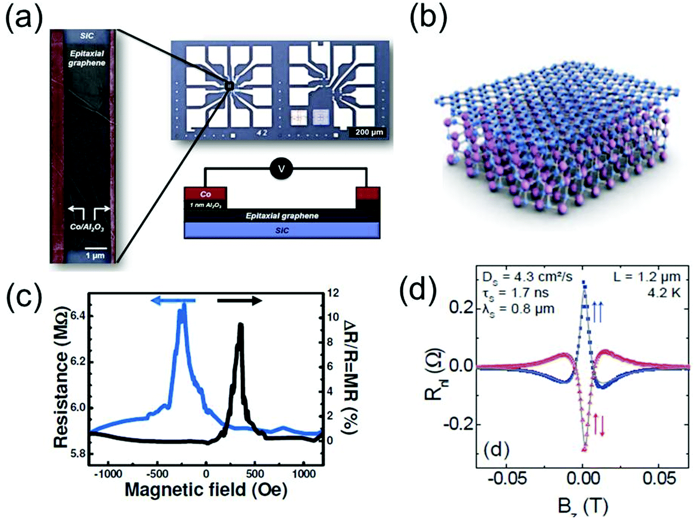 | ||
| Fig. 71 (a) Typical two-terminal local spin valve device. The width of graphene channel on SiC is 10 μm, and the distance between the two Al2O3/Co electrodes is L = 2 μm. The optical image shows the entire structure, including contact pads. (b) Atomic arrangement of SLG on SiC. (c) Large local resistance spin signals measured at 4 K. (d) Oscillating and decaying device non-local resistance as a function of the applied magnetic field (Hanle measurement). Adapted from ref. 223, 1300. | ||
Following what is known for metals and semiconductors, two mechanisms are currently believed to take place in graphene: Elliot–Yafet (EY)232,233 and Dyakonov–Perel (DP).162 In EY the electron spin has a finite probability to flip during each scattering event off impurities or phonons.232,233 The DP mechanism is driven by the precession of electron spins along effective magnetic field orientations, which depends on the momentum, and with direction and frequency of precession changing at each scattering event.162 The most recent theoretical derivation in SLG (taking into account the Dirac cone physics) reports a spin relaxation time varying proportionally to the transport time, behaviour typical of the EY-relaxation.1273
A primary objective in the near future is to clarify the true nature of the dominant mechanisms determining the spin relaxation time and spin relaxation length in high quality graphene devices. Indeed, while spin transport in graphene has been demonstrated by several groups worldwide, the full understanding of spin dynamics and relaxation is still lacking, and theoretical predictions or generalization of the EY and DP-relaxation mechanisms seem unable to cope with the experimental reality.1276 Recent results indicate that the situation can be improved by a precise tuning of the contact resistance between graphene and magnetic electrodes,223 but it is still unclear what this implies for large scale RT devices. More effort is thus needed in order to explore the spin relaxation mechanisms from a theoretical perspective beyond the conventional perturbative treatments. Spin relaxation time and the g factor (or dimensionless magnetic moment) need to be evaluated by taking into account the relevant scattering processes close-to and away-from the Dirac point (short and long range scatterers, e–e and e–ph interaction etc.), depending on the intrinsic and extrinsic nature of scattering sources, and for the main classes of materials of relevance for RT operability.
Simultaneously, a global and comprehensive understanding of spin relaxation mechanisms needs to be established based on the existing information and more targeted and systematic experiments combining two-terminal magnetoresistance and four terminal Hanle transport measurements (see Fig. 71) and disentangling the contribution of contacts from intrinsic spin relaxation induced by defects, disorder, interaction with substrate, etc. This is a major bottleneck, which demands a concerted effort between experiment and theory.
6.2. Spin injection in graphene
The variety of favourable properties for spintronics that graphene provides include also efficient spin injection,223 due to the tunability of the Fermi level. The large electron velocity implies that graphene has unique properties for the transport of spin polarized currents to long distances.223 The analysis of scattering mechanisms is necessary in order to achieve optimal production methods for graphene-based spin-valves. The optimization of performances of graphene spin-valve devices is required, comprising a focus on the specific role of magnetic contacts, including their spin injection and detection efficiencies and the possible role of interface effects in spin relaxation and spin dephasing.Interface engineering to optimize spin injection and detection from a ferromagnet into graphene still remains a very challenging issue and it represents one of the main bottlenecks. Systematic investigations of the role of the tunnel barrier have been slow because of the difficulties of growing uniform, ultrathin insulating layers on graphene. Any irregularity during growth would favour the formation of pinholes. Alternative barriers and spin injection and detection methods should also be explored.
While in early devices spin injection was achieved using transparent contacts (Co/SLG),1281 a great improvement on both injection efficiency and spin lifetime was obtained with tunnelling contacts (Co/Insulator/SLG).1282 One of the main issues in conventional interfaces remains, however, the matching of conductances. For this purpose, interfaces of graphene with graphite intercalated with magnetic impurities or molecules (similarly to magnetic semiconductors1283,1284) seem viable and have to be explored more deeply. The spin valve1285 is the natural bench to test the efficiency of spin injection with graphene hybrids.1286 Further optimization of the ferromagnetic contacts for both spin injection and detection is also possible. Currently, oxide tunnel barriers, such as Al2O3 and MgO, are common choices, but new barrier materials and new technologies based on (single) atomic layer deposition of BN, and related materials like MoS2 and MoSe2, to make tunnel barriers of single or few atomic layer thicknesses, should be considered. Other concepts involving the spin Hall effect (SHE),234 which is the formation of spin-polarized current driven by spin–orbit coupling introduced by impurities, should also be explored;1287,1288 especially owing to the highly efficient spin current generation observed in materials such as Ta due to SHE.1289 Spin injection is currently performed and deeply investigated in both SLG and BLG,1290 and measurements on FLG and MLG up to 40 nm thick have been reported.1291–1293 Further experiments require unambiguous assessment of the potential of all of these and identifying, in each case, the phenomena that determine the experimentally observed spin injection/detection efficiency. It is also crucial to investigate the integration between the graphene channel and different materials as substrates.
The development of new device fabrication and innovative spin manipulation protocols would advance spin injection efficiency at the ferromagnet/graphene interfaces, data recording and spin information processing. More exciting is the design of novel spintronic devices at <10 nm scale. Here, components enter in the quantum regime, and graphene may exploit the crossover between classical and quantum features of such nano-elements.
6.3. Graphene spintronic devices for sensing
The long spin diffusion length in graphene could enable its use in spintronic based magnetic sensors. It was shown1294 that graphene has a large non-local spin current effect near the Dirac point up to RT, and at small magnetic fields (0.1 T). Graphene spintronics has thus the potential to revolutionize the development of magnetic sensors with sensitivity ranging from the nT to the pT ranges (for comparison, the Earth's magnetic field is in the μT range1295). The potential of lab-on-chip spintronic sensors for magnetic nanoparticles would also impact onsite drug delivery control or tumour disease fight medicine. Additionally, breakthroughs in the fields of MRAM and reconfigurable logic have a cross-disciplinary interest for ICT.1296 Intrinsic non-volatility of spintronics technologies presents a significant advantage in terms of power consumption. The power consumption reduction will benefit as much for tightening supplies of energy, as for the digital societal revolution of ever more demanding portable electronics. The radiation hardness of spintronics metal-based technologies1297 is also an advantage, in particular in aerospace. The coupling of spin information with optics could lead to spin information transmission by optical links. Finally, spintronics already mainly relies on low-dimensional quantum limits, and can be downscaled without increasing power consumption.12986.4. Graphene spin gating
Graphene's intrinsic features are ideal not only for downscaling of conventional devices, but also to demonstrate radically new ideas that will allow spin manipulation without the trade-off related to the reduction of spin coherence time. New concepts to be explored include tailoring spin degrees of freedom through magnetic proximity effects (magnetic gating), torque effect, the SHE, mechanical strain or molecular/atomic functionalization, all requiring the networking of interdisciplinary research communities.In addition to ballistic transport and micron long mean free paths145 spin relaxation lengths can reach unrivalled values1280 opening new avenues for spin manipulation in lateral graphene spin devices. Several ways can be explored to manipulate spin polarized (and eventually pure spin) currents. To that end, once long lifetime of injected spin-polarized electrons has been achieved, the next challenges lies in the engineering of tuneable magnetism or spin gating (i.e. external action on the electron spin to implement spin-based information processing technologies). Such strategy could be explored by evaluating the (spin)-transport response of gated devices to magnetic moments induced in graphene by external means, such as hydrogenation, defects, strain engineering or other methods (a schematic of intentional and external perturbations is shown in Fig. 72) or structuring the lattice as a nanomesh.1299 By tackling these issues, one anticipates the eventual demonstration of external ways to control (through gates or possibly multi-gates) the propagation of spin currents, achieving operational reliability at RT and architectural compatibility with Si technologies.
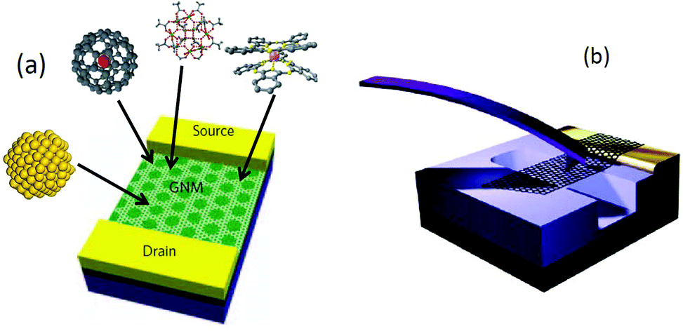 | ||
| Fig. 72 (a) CMG using molecular adsorption or nanomesh patterning. (b) Mechanical strain applied on the graphene device. | ||
Other types of proximity effects can also be harnessed, including effects on the electronic and spin properties induced by the interface with insulating magnetic materials, magnetic molecules, materials having a large spin–orbit coupling, ferroelectric materials. We refer, e.g., to the theoretical prediction of spin polarization induced by an interface with Europium oxide,228 or Yttrium Iron Garnet (YIG) and/or a material with strong spin orbit interaction.228 Such mechanism would not require any ferromagnetic metallic contact to inject spin-polarized electrons. Thus, it could be a way to circumvent the conductivity mismatch. Similarly, the exploration of the potential of graphene where the injected spin-polarized charges flows in close proximity of, and interacts with, other extrinsic spins (in localized or more extended charged states, located below or on top of the graphene) is very appealing.1300
6.5. Graphene qubits
By trapping an odd number of electrons on a dot one can create an electrically controlled localised spin state,1301 allowing the implementation of so-called spin qubits,1301 which can be used for quantum information processing.1301 Several proposals to use GQDs for quantum information processing have already been made,1298 based on the long spin memory of electrons in graphene (in particular, due to the absence of nuclear spin environment, a major problem for the use of III–V semiconductor dots for quantum information processing1302).An additional possibility to create GQDs is related to the unique properties of BLGs. In BLGs, transverse electric fields can be used to open a gap. One can confine electrons in small regions of a BLG using a combination of top/bottom gates, and, then, operate the charging states of such QDs electrostatically. Further studies of gap control and electron confinement in gapped BLGs are needed. An intriguing challenge is to couple GQDs with other quantum systems. Amongst these, molecular nanomagnets (e.g. single molecular magnets, spin transition compounds) have shown considerable potential, due to the control of their quantum features at the molecular level.955 Moreover, the ability to control/functionalize the external shell of such molecules, allowing one to graft them on carbon surfaces, makes the realization of molecule-graphene hybrids feasible. The choice of substrate and spin state of the deposited molecule make hybrid carbon-based molecular architectures a promising platform to design novel spintronic devices, e.g. molecular spin valves in vertical geometry made by graphene sandwiched between a magnetic substrate and a magnetic molecule. Another possibility is to investigate – at higher T – the spin split of the energy band induced by magnetic molecules deposited on top of graphene. These are just few examples of the opportunities that molecular quantum spintronics based on low dimensional carbon materials may open.
6.6. Spintronics using other 2d crystals and heterostructures
In spin transfer torque (STT) experiments the orientation of a magnetic layer in a magnetic tunnel junction or spin valve can be modified using a spin-polarized current.1303 STT-based memory technology relies on magnetization switching induced by spin currents, and stands as a foreseen direction of innovation for spintronics. Demonstrations of perpendicular STT devices,1304 switching of ferromagnets using pure spin currents and spin Hall torque devices,1305 voltage-controlled switching of magnetic tunnel junctions (MTJs),1306 and novel spin logic architectures1307 have been reported using hybridization of magnetic materials and semiconductors, although their operational capability remains insufficient for the advent of practical (RT and upscalable) spin-based memory and logic technology technologies.The portfolio of 2d materials offers many perspectives for the design of new interfaces and hybrid heterostructures using semiconducting 2d systems (MoS2, WS2, …) and magnetic materials (ferromagnetic metals, insulators) which could support the development of STT-based novel devices, circuits and architectures.
Some theoretical studies have suggested1308 that MoS2, normally a nonmagnetic, direct band gap semiconductor, acquires a net magnetic moment upon adsorption of specific transition metal atoms (such as Mn), as well as Si and Ge atoms [see e.g.ref. 1309]. This permits the diversification of the class of materials which can be combined and engineered for the implementation spin-based properties.
2d semiconducting materials may also allow the manipulation of other quantum degrees of freedom, such as valley degeneracy. This gives rise to the possibility of valleytronics,31 relying on the fact that the conduction bands of some materials have two or more minima at equal energies, but at different momentum space positions. To engineer a valleytronic device, the number of electrons per valley must be controlled to monitor valley polarization. In this respect, 1L-MoS2 is particularly promising because conduction and valence band edges have two energy-degenerate valleys at the corners of the first Brillouin zone. Ref. 1310 reported that optical pumping with circularly polarized light could achieve a valley polarization of 30% in 1L-MoS2, pointing towards optical valley control and valley-based electronic and optoelectronic applications in 1L-MoS2.
6.7. Theory and quantum simulation
Experimental studies need to be backed by advanced spin transport simulations, based on a multiscale approach combining ab initio calculations with tight-binding models for material parameterization (material structure, defects, deposited magnetic oxides, ad-atoms and adsorbed molecules) with semi-classical or quantum transport methods following spin diffusion. First principles and tight-binding calculations of SLG and BLG covered with vacancies, hydrogen ad-atoms, magnetic molecules and deposited magnetic oxides (in the presence of external electric fields) have the potential to clarify the effects of spin–orbit coupling and magnetic interactions on induced spin relaxation and spin–orbit transport. Moreover, transport lengths scales (mean free path, spin diffusion length, etc.) and transport tunability could be established by spin-dependent transport calculations through efficient quantum transport methodologies, providing guidance505 on spin relaxation mechanisms and gating efficiency of spin polarized currents in chemically/structurally modified devices.6.8. Outlook
The aim is to reach the ultimate potential of graphene for spintronics, targeting efficient spin injection and detection, but also spin gating and spin manipulation. By investigating spin-based information technology methods supported by concrete demonstrations as well as modelling, the development of new ideas and implementations of graphene-based systems can be foreseen. The achievement of these tasks would pave the way towards all-graphene-based integrated MRAM and Spin information processing based circuits.High priority has to be given to the evaluation of materials and device's architectures in view of future industrial applications. An exhaustive evaluation of feasibility among materials and their properties, fabrication techniques and designs need to be undertaken, in terms of quality, optimization, upscalability, reproducibility and RT operability.
Over the next 10-years (see Fig. 73) it is imperative to design, engineer and address large scale manufacturability of these highly advanced spintronic devices and architectures.
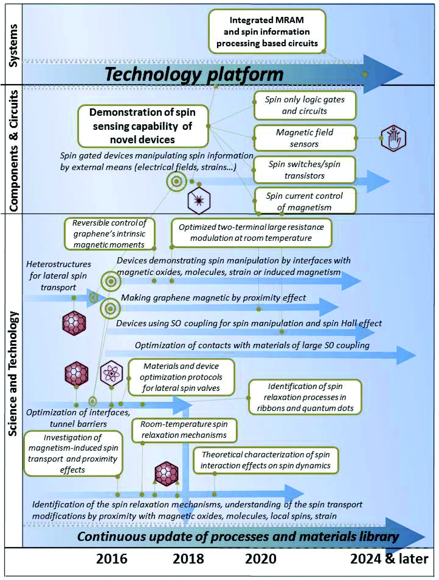 | ||
| Fig. 73 Spintronics timeline. | ||
Using the intrinsic molecular and 2d properties of graphene, the high-impact perspective is to combine the unique long spin lifetime and high mobilities with new paradigms to manipulate the spin information locally, towards a new generation of active, CMOS-compatible, molecularly-engineered spintronic devices, with possible low-energy operation. The explored concepts could use magnetic proximity effects, the SHE, mechanical strain and molecular/atomic functionalization, as well as spin torque induced switching. Overcoming these challenges would pave the way to all-spin-based information processing technology, with capabilities ranging from replicating conventional electronics, to quantum information processing, and advanced functionalities.
The timeline for spintronic applications of GRMs is shown in Fig. 73. Timescales: 3–4 years: acquiring a comprehensive picture of spin relaxation mechanisms at RT in graphene, fundamental for controlling detrimental effects of material structural imperfections, environmental perturbations on spin transport. 5–9 years: demonstration of a spin gating functionality to prove that spin can be manipulated in some way (again for practical reasons, this has to be achieved at RT). Several routes need to be explored, such as chemical functionalization or strain fields, with which some tunability of the spin–orbit coupling and resulting spin transfer can be envisioned. Over 10 years: device-oriented integration, including the search for all-spin based architectures and co-integration of computing and data storage using the same material platform (i.e. wafer-scale graphene), targeting RT operation.
7. Photonics and optoelectronics
Graphene is emerging as a viable alternative to conventional optoelectronic, plasmonic and nanophotonic materials.995 It has decisive advantages, such as wavelength-independent absorption,784 tunable optical properties via electrostatic doping,1311 large charge-carrier concentrations,179,752,1312 low dissipation rates and high μ,99 and the ability to confine electromagnetic energy to unprecedented small volumes.1313Fig. 74 and Table 4 show some possible applications, drivers and an indication of when functional device prototypes could be expected. We envision breakthroughs in highly-integrated and high-speed graphene optoelectronics, long-wavelength photodetection and THz operation, ultrafast pixelated photodetection, broad-band tunable lasers, high efficiency photodetection and PV, and tunable optical metamaterials and plasmonic nano-optoelectronic circuits.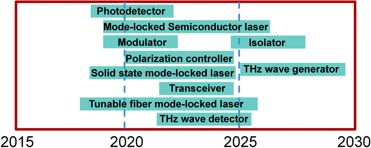 | ||
| Fig. 74 Graphene photonics applications timeline. The rectangles in the figure indicate the timeframe when functional device prototypes could be expected. | ||
| Application | Drivers | Issue to be addressed |
|---|---|---|
| Photo-detector | Fast increase of bandwidth chip to chip/intra-chip. | Need to increase responsivity, which might require a new structure, plasmonics and/or doping control. |
| Higher bandwidth per wavelength not possible with IV or III–V detector in 2020. | ||
| High photoconductive gain. | ||
| Graphene photo-detector can increase bandwidth per wavelength to 640 GHz. | ||
| Graphene photo-detector can detect VIS, Infrared and THz. | Modulator bandwidth has to follow suit. | |
| Mode-locked semiconductor laser | Bandwidth increase between core to core and core to memory requires optical interconnect with over 50 wavelengths, not possible with a laser array. | Competing technologies: actively mode-locked lasers or external mode-lock lasers |
| GSA enables passively mode-locked semiconductor and fibre lasers, candidates for dense wavelength division multiplexer (D-WDM). | Interconnect architecture should consume low power. | |
| Solid-state mode-locked laser | GSA can be simpler and cheaper and easy to integrate into the laser system. | Need cost effective graphene transfer technology. |
| Tuneable mode-locked laser | Wide spectral range of graphene is suitable for widely tuneable mode-locked laser. | Need a cost effective graphene transfer technology. |
| Optical modulator | Si operation bandwidth limit ∼50 GHz. Graphene is a good candidate without using complicated III–V epitaxial growth or bonding | High quality graphene with low Rs is key for increasing bandwidth over 100 GHz. |
| Improve ION/IOFF. | ||
| Polarization controller | Current polarization controlling devices are bulky and/or difficult to integrate. | Need to improve controllability. |
| Graphene can realize compactness and integration of these devices. | ||
| Isolator | Graphene can provide integrable and compact isolators on Si substrate, otherwise only possible with bulky magneto optical devices | Decreasing magnetic field and processing are important to products |
The dispersion relation remains quasi-linear up to ∼±4 eV from the Fermi energy.141 It is therefore possible to generate charge carriers in graphene by optically stimulating inter-band transitions over a wide energy spectrum, unmatched by any other material. This includes commercially important telecommunication wavelengths and the FIR/THz and the SWIR (short-wavelength infrared) and MIR (mid-infrared) regimes (see Fig. 75a).
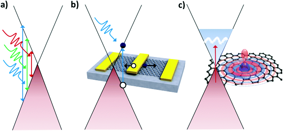 | ||
| Fig. 75 Schematics of (a) wavelength-independent absorption, (b) broadband photodetection, (c) plasmon generation by a molecule or through a plasmon resonance. | ||
The high μ enables ultrafast conversion of photons or plasmons to electrical currents or voltages (Fig. 75b). By integration with local gates, this process is actively tuneable and allows for sub-micron detection resolution and pixelization.
Graphene electronic and photonic devices can be fabricated using standard semiconductor technology, which facilitates monolithical integration into Si-based mass-production platforms. This is a decisive advantage over most other promising nanotechnologies.
At elevated (>1013 cm−2) carrier densities, graphene supports surface plasmons with unprecedented properties:1313 (i) Extreme confinement, 1–3 orders of magnitude smaller than the wavelength,1313 much smaller than the confinement of plasmons in noble metals in the considered spectral regime. (ii) The optical response of graphene plasmons is strongly dependent on the doping level, i.e. the Fermi energy relative to the Dirac point. This can be changed electrostatically, providing a tool for ultrafast electro-optical switching and modulation. (iii) Crystallinity and defect-free structures over large distances due to the strength of the carbon bond, in contrast to plasmonic metals, in which fabrication imperfections constitute a bottleneck in the performance of nano-metallic structures. (iv) Low losses, resulting in surface plasmon lifetimes reaching hundreds of optical cycles.1313
Electrostatically controlled Pauli-blocking of optical transitions and controlled damping of plasmon propagation enables the realization of ultra-high bandwidth electro-optical modulators,1314 optical switches, and similar devices.
Graphene is an excellent candidate for high-gain photodetection by employing the photogating effect.1315 Because of its very high μ and its 2d nature, its conductance is very sensitive to electrostatic perturbation by photogenerated carriers close to the surface.
The graphene properties that may appear to hinder its development for purely electronic devices, such as the absence of a band-gap, are not critical for photonics and optoelectronics. In fact, they can be beneficial, enabling ultra-wideband accessibility provided by the linear electronic dispersion, allowing efficient, gate controllable, e–h pair generation at all wavelengths, unlike any other semiconductor.
Based on these unique optoelectronic properties, a wide range of applications can be developed. Here, we summarize a selection of those for which we see technological breakthroughs in the near-future:
Highly-integrated graphene photonics. The compatibility of graphene with standard CMOS processes at wafer scale makes it a promising candidate for high data-rate (inter- and intra-chip) optical interconnects. Graphene might allow the realization of high-speed, compact-footprint electro-optical modulators, switches and PDs, integrated with Si waveguides or plasmonic circuits. The mechanical flexibility of graphene may also enable the integration with bendable substrates and plastic waveguides.
Long-wavelength light detection. Graphene enables light detection at wavelengths beyond the current limit set by the band gap of traditional semiconductors, opens up new applications in the FIR (THz) and SWIR and MIR regimes (e.g. bolometers and cameras), and has potential for ultrafast pixelated detection with ballistic transport of generated charge carriers.
Terahertz operation. This will enable products such as portable sensors for remote detection of dangerous agents, environmental monitoring or wireless communication links with transmission rates above 100 Gbit s−1.
High-efficiency photodetection. The target is the realization of highly efficient photocurrent generation by providing a gain mechanism where multiple charge carriers are created from one incident photon.
Plasmonics and metamaterials. Graphene surface plasmons as well as tailored metal nanostructures can be exploited to enhance and control the coupling between light and graphene. This will pave the way to ultra-fast optical switching, ultra-strong light-absorption, PVs, and single bio-molecule sensing.
Photonic integrated circuits. The target is to develop active optoelectronic devices and co-integrate these with passive optical components, such as waveguides,(de-)multiplexers and filters. Device functionalities comprise the switching and routing of light at ultra-fast speeds and at nano-scale dimensions, converting broadband incident light into detectable electrical signals.
Lasers. Exploiting the broadband saturable absorption properties of graphene, the aim is to realize mode-locked lasers (e.g., fiber, semiconductor, waveguide and solid state lasers) with broad tunability and bandwidth in the telecommunications and mid-IR range, compared to existing technologies.
The vision is to establish a new field of GRM photonics, sustained by the convergence and co-integration of GRM-based electronic and photonic components such as lasers, optical waveguides, cavities, modulators, photodetectors, and solar cells.
GRMs may be employed as active optoelectronic materials to achieve light–matter interaction, convert incident light energy into detectable electrical signals, and, vice versa, electrical signals may be used to modulate light and realize optical switches. For this purpose, GRMs should be integrated with established and mature technologies, such as dielectric (Si or plastic) waveguides, optical antennas, plasmonic structures (e.g. gratings or nanoparticles), metamaterials, QDs, etc. Graphene's constant optical absorption over a spectral range covering the THz to the UV allows light detection over a wavelength range superior to any other material. Combined with its high μ and Fermi velocity, this implies that devices operating in the hundreds of GHz range are feasible.
Despite graphene's absorption of 2.3% being large once its monoatomic thickness is considered, it is still necessary to increase this value to allow more efficient light–matter interaction and realize highly efficient optoelectronic devices. For this purpose, several routes can be pursued. One is the combination of graphene with plasmonic nanostructures,446 whereby the near-field enhancement due to localized surface plasmons can significantly increase the light absorption.446 In principle, structures can be designed to achieve 100% light absorption.446 Semiconducting nanoparticles of various shapes and forms can also be used to improve the quantum efficiency.1315 Light harvesting and concentration with these nanostructures into graphene leads to increased absorption and more efficient conversion of light into electrical signals, with an increase of quantum efficiency.
Another concept involves the integration of graphene with highly confined optical waveguides, such as Si-on-insulator (SOI) waveguides, widely used in highly-integrated Si photonics. As light propagates along the waveguide, it is absorbed along the length of the propagation and 100% light absorption might be possible.1316–1318 Graphene may also be inserted between two mirrors to form microcavity-integrated optoelectronic devices.1319 The incident light is reflected by the top and bottom mirrors and passes through the graphene multiple times. At the resonance condition, constructive interference enhances the optical field in the cavity, leading to enhanced light–matter interaction and strong optical absorption.
The exploitation of plasmons in graphene itself is raising interest.252,266,273,1320–1326 The resulting strong light–matter interaction can be further utilized to enhance detector performance as well as to enable radically new light sensing concepts.
The ever increasing demand for higher-bandwidth brings along the need for higher-bandwidth devices on the transmitting, as well as the receiving side, of the communications link. As large parts of the internet traffic are already transmitted optically, the need for high-speed modulators and photodetectors in the telecommunications wavelength range (1.3–1.55 μm) is ever more pressing. Moreover, optical interconnects are currently being introduced as a way to link computers to mobile devices, as well as ultra-high bandwidth links for inter- and even intra-chip communication. It was demonstrated that graphene photodetectors are capable of supporting bandwidths up to 262 GHz,1327 a huge value, but still far below the intrinsic limit, thus far estimated in the THz range.1328 The speed limit of graphene-based PDs needs to be established. Devices need to be optimized in terms of responsivity, by enhancement with plasmonics and quantum structures, as well as integrated into optical cavities and waveguides. Electro-optical modulators need to be realized and benchmarked in terms of speed and other parameters.
The FIR (THz) and MIR regions are fairly unexploited parts of the electromagnetic spectrum, and especially light detection is difficult as the THz photon energy is below the thermal energy. However, many interesting applications can be thought of, due to the non-ionizing and low-energy characteristics of THz and MIR radiation. Ranging from medical applications, such as cancer diagnostics, to security, such as explosive detection, since all materials have characteristic fingerprints in the THz/MIR region, a very wide application range is feasible. Further, active devices working in the THz/MIR range are crucial to convert very high frequency signals (in particular, the THz/MIR part of the solar radiation spectrum) into DC voltage – a feature which could eventually lead to self-powered devices. Having zero-band gap, graphene offers huge potential to outperform all available semiconductor technologies in the THz and MIR range, to reach THz operation frequencies, and to enable future wireless THz systems.
Graphene-based sensing and imaging in the SWIR is another interesting area that lies at the heart of safety and security applications in civil and military surveillance, night vision applications, automotive vision systems for driver safety, food and pharmaceutical inspection and environmental monitoring, just to name a few. The SWIR region is so far based on the use of III–V single crystalline semiconductors for sensing. Imaging has curtailed their monolithic integration to CMOS read-out integrated circuits (ROIC) and focal plane arrays (FPAs).1329 This results in SWIR imaging sensors at a 3-order-of-magnitude greater cost compared to visible-wavelength Si-based ones,1330 and pixel resolution limited to ∼1 MP (mega pixel) range,1330 as opposed to tens of MPs offered by current CMOS imaging sensors.
The 2d nature of graphene makes it also feasible to use CMOS-compatible processing techniques with CVD grown large-area graphene, in order to achieve highly-integrated arrays consisting of numerous individual devices. This may allow the fabrication of pixelated graphene-based cameras working over an ultra-wide spectral range, enabling image capture from the visible to the more unexplored THz/MIR range. Potential application areas include medical, automotive and security, such as tissue imaging, driver supporting head-up displays, and explosive/biological species detection.
Current solar cell technologies use only a rather small part of the solar spectrum due to their intrinsic band gap limiting the maximum detectable wavelength.1331 The absence of a band-gap in graphene translates into the absence of this maximum detectable wavelength limit and, combined with its constant absorption, solar energy over a much wider spectral length might be converted to electricity. Solar cells based on graphene, as well as combined with plasmonic and quantum nanostructures, thus need to be explored.
Graphene can be combined with other nanostructures, taking advantage of the strong light absorption in QDs and the 2-dimensionality and high μ, to merge these materials into a hybrid system for photodetection with high sensitivity.1315 Further, the integration with plasmonic metamaterials will enable a new class of optical switches for displays.
Surface enhanced Raman Spectroscopy (SERS) can in principle achieve signal enhancements of up to 1015.1332 Plasmonic nanostructures enhanced sensing may lead to detection limits on the single-molecule level. The near-field enhancement resulting from the combination of graphene with plasmonic nanostructures1333 will increase the signal sufficiently.1334 Such structures will also benefit from graphene's compatibility with biological species. Combined with graphene's single-electron charge sensitivity, we expect this technology to become a new platform for medical applications, not only providing enhancement at the single-molecule sensing level, but also being bio-compatible.
Integration of graphene into a cheap, flexible sensing platform based on plastics must be explored. It is envisaged to integrate and merge the aforementioned medical and THz/MIR sensors with plastic electronics to achieve a sensing-platform for wearable electronics, as well as low-cost one-time use sensors for use in developing countries.
7.1. Graphene saturable absorbers and related devices
Materials with nonlinear optical and electro-optical properties are needed in most photonic applications. Laser sources producing nano- to sub-ps pulses are key components in the portfolio of leading laser manufacturers. Regardless of wavelength, the majority of ultrafast laser systems use a mode-locking technique, where a nonlinear optical element, called a saturable absorber (SA), turns the continuous-wave output into a train of ultrafast optical pulses.1335 The key requirements are fast response time, strong nonlinearity, broad wavelength range, low optical losses, high power handling, low power consumption, low cost and ease of integration into an optical system. Currently, the dominant technology is based on semiconductor SA mirrors (SESAMs).1335,1336 However, these have a narrow tuning range, and require complex fabrication and packaging.1335,1353 The linear dispersion of the Dirac electrons in graphene offers an ideal solution: for any excitation there is always an e–h pair in resonance. The ultrafast carrier dynamics512,513,1337,1338 combined with large absorption171,990 and Pauli blocking, make graphene an ideal ultrabroadband, fast SA.1339,1353 Unlike SESAMs and CNTs,1340–1352 graphene does not require bandgap engineering or chirality/diameter control.1339,1353Since the first demonstration in 20091353 (Fig. 76), the performance of ultrafast lasers mode-locked by graphene has improved significantly. E.g., the average output power has increased from a few mW1353 to over 1 W.1354 LPE1339,1353,1355–1359 CVD,1360,1361 carbon segregation,1362 MC1359,1363 have been used for graphene saturable absorber (GSA) fabrication. So far, GSAs have been demonstrated for pulse generation at 1,1369 1.2,1370 1.51339,1353,1360,1363,1366 and 2 μm.1364 The most common wavelength is ∼1.5 μm, not due to GSAs wavelength restriction, but because this is the standard wavelength of optical telecommunications. Ref. 1356 reported a widely tuneable fiber laser mode-locked with a GSA. The laser produces ps pulses in a tuning range 1525–1559 nm, demonstrating its “full-band” operation performance.
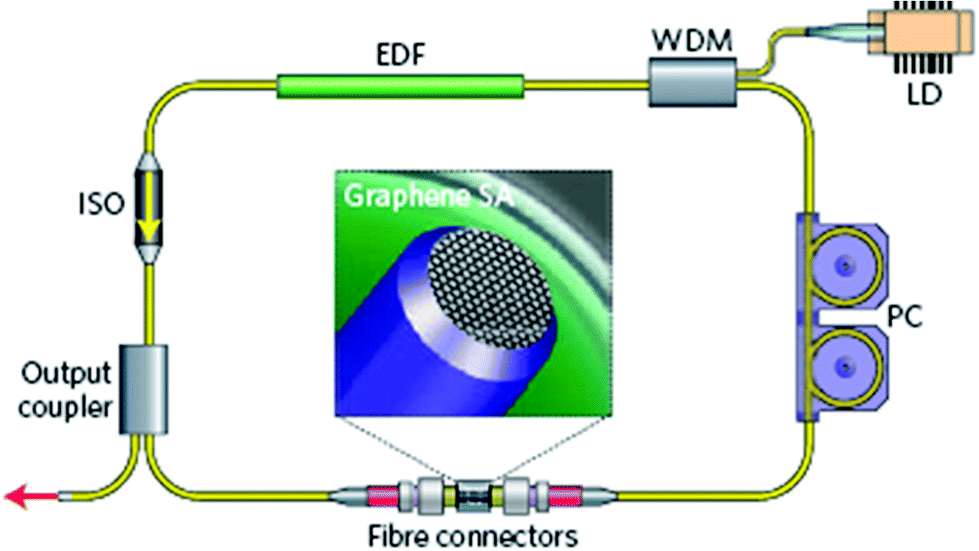 | ||
| Fig. 76 Graphene fiber laser.1353 WDM, wavelength division multiplexer; PC, polarization controller; EDF, erbium-doped fiber; ISO, isolator.995 | ||
Fiber lasers are attractive due to their efficient heat dissipation and alignment-free format.1365 GSAs have been used to mode-lock fiber lasers.1339,1353,1355–1357,1360,1363,1366 For fiber lasers, the simplest and most economical approach for GSA integration relies in sandwiching directly the GSA between two fiber connectors (Fig. 76) [see ref. 1356, 1360, 1363, 1366 and 1339]. Other options (e.g. evanescent-wave based integration1367) have also been demonstrated for high-power generation. Sub-200 fs pulses were achieved using a stretched-pulse design, where the cavity dispersion is balanced to stretch the pulse for the limitation of nonlinear effects.1355
Solid-state lasers are typically used for high-power output, as alternative to fiber lasers.1368 GSAs have also been demonstrated to mode-lock solid-state lasers.1369–1372 In this case, CVD graphene (>1 cm2) was directly transferred to a quartz substrate.1370Ref. 1370 reported 94 fs pulses with 230 mW output power. Another approach for GSA fabrication relies in spin-coating LPE graphene either on quartz or high-reflectivity mirrors. GSA can then be inserted into a solid-state cavity. This was used to achieve average power up to 1 W using a solid-state Nd:YVO4 laser,1372 with ∼1 μm output wavelength and ∼14 nJ energy.
SLG grown via CVD was also used in ultrafast vertical-external-cavity surface-emitting lasers (VECSELs).1361 A VECSEL consists of an external cavity, formed by high-reflection mirrors, and an output coupler, with typical cavity lengths of a few mm up to tens of cm.1335,1373 The gain chip generally contains a highly reflective bottom section to reflect the laser and pump light, an active semiconductor gain section, and an anti-reflective top layer.1335,1373,1374 VECSELs combine the advantages of semiconductor lasers, such as compact footprint (down to ∼3 mm cavity1375), with those of diode pumped solid-state lasers, such as low timing jitter,1376 excellent beam quality,1377 high average1377 and peak power1378,1379 VECSELs are mode-locked by SESAMs, epitaxially grown on lattice-matched semiconductor substrates.1335 However, SESAMs only offer a limited operation bandwidth (to date, the broadest tuning range of VECSELs mode-locked with SESAMs is 13.7 nm1380). Ref. 1361 controlled the electric field intensity in SLG by changing its absorption on a high-reflection mirror. The resulting SLG-based saturable absorber mirrors (GSAMs) have shown an unsaturated loss adjustable from 0 up to 10% and modulation depth up to 5%.1361 These enabled to mode-lock a VECSEL with a series of different gain chips over a 46 nm wavelength range (from 935 to 981 nm) with repetition rates up to 2.48 GHz, and 466 fs pulse duration. These results can lead to novel graphene-based ultrafast light sources to meet the wavelength range, repetition rate and pulse duration requirements for various applications (e.g. metrology, spectroscopy and data-communication).
Graphene is also promising for other photonic applications, such as optical limiters1381 and optical frequency converters.1381 Optical limiters are devices that have high transmittance for low incident light intensity and low transmittance for high intensity. There is a great interest in these for optical sensors and human eye protection,1381 as retinal damage can occur when intensities exceed a certain threshold.1381 Passive optical limiters, which use a nonlinear optical material, have the potential to be simple, compact and cheap.1381 However, so far no passive optical limiters have been able to protect eyes and other common sensors over the entire visible and NIR range.1381 Typical materials include semiconductors (e.g. ZnSe, InSb), organic molecules (e.g. phthalocyanines), liquid crystals and carbon-based materials (e.g. carbon-black dispersions, CNTs and fullerenes).1382 In graphene-based optical limiters the absorbed light energy converts into heat, creating bubbles and microplasmas,1382 which results in reduced transmission. Graphene dispersions can be used as wideband optical limiters covering visible and NIR. Broad optical limiting (at 532 and 1064 nm) by LPE graphene was reported for ns pulses.1382Ref. 1383 reported that FG dispersions could outperform C60 as an optical limiter.
Optical frequency converters are used to expand the wavelength accessibility of lasers (e.g., frequency doubling, parametric amplification and oscillation, and four-wave mixing).1381 Calculations suggest that nonlinear frequency generation in graphene (e.g. harmonics of input light) should be possible for sufficiently high external electric fields (>100 V cm−1).1384 Second-harmonic generation from a 150 fs laser at 800 nm was reported.1385 In addition, four-wave mixing to generate NIR tunable light was demonstrated using SLG and FLG.1386 Graphene's third-order susceptibility |χ3| was measured to be ∼10−7 e.s.u.,1386 up to one order of magnitude larger than CNTs.1386 Other features of graphene, such as the possibility of tuning the nonlinearity by changing N, and wavelength-independent nonlinear susceptibility1386 could be used for various photonic applications (e.g. optical imaging).
The main parameters of a pulsed laser are output power (or single pulse energy), output spectral coverage (e.g. operation wavelength, wavelength tuneability), pulse duration and repetition rate. The requirements for ultrafast laser are highly application-dependent. E.g., for fiber-optical communications, the operation wavelength is ∼1.5 μm as optical fibers have low loss and low dispersion around this spectral range.1387 For medical applications (e.g. laser surgery), the required laser operation wavelengths mainly depend on the peak absorption of different tissues.1388,1389 These range from MIR for minimally invasive surgery of skin cutting,1390 to UV for athermal photoablation.1391 For high-speed fiber-optical signal transmission and processing, high-repetition rate (>GHz) allows the signal to carry more data, while for industrial material processing (e.g. micro-machining), kHz pulses are commonly used to decrease the cumulative heating caused by multiple laser pulses.1392 In general, high output power, wide spectral coverage, short pulse width, and high repetition rate are desirable, because it is easy to reduce the output power (e.g. by attenuators), narrow the spectral coverage (e.g. by optical filters), broaden the pulse duration (e.g. by dispersive fibers) and decrease the repetition rate (e.g. by optical choppers), but not vice-versa. Furthermore, stability, cost, compactness and efficiency (e.g. electrical-to-optical or optical-to-optical efficiency) also are key for applications.
1408 have been used as SA for ultrafast pulse generation. Tunable output results have been demonstrated.28 Thus far, 2d crystals-based ultrafast lasers only have been demonstrated on erbium-doped fiber lasers (EDFLs)1402,1404–1407 and thulium/holmium co-doped fiber laser.1403 However, it is expected that other 2d crystals will soon be employed on other lasers (e.g., ytterbium-doped fiber lasers – YDFL-, thulium-doped fiber lasers TDFL and solid-state and waveguide lasers as well).1058
Ref. 1409 reported resonant nonlinear optical susceptibilities at the edges of MoS2 flakes, allowing direct optical imaging of the atomic edges and boundaries of such 2d crystal. Indeed, the structural discontinuity at the edges and boundaries of 2d crystals, e.g., graphene and TMDs, leads to complex interplay between the atomic positions and the electronic structures.1409 Subsequently, the atomic edges and boundaries reconstruct structurally and electronically due to the translational symmetry breaking.1409Ref. 1409 developed a nonlinear optical imaging technique that allows rapid and all-optical determination of the crystal orientations of the MoS2 at a large scale. Moreover, zigzag nanoribbons showed a two-photon resonance at ∼0.8 eV, originating from the subband transitions from the valence bands to the isolated edge states of the Mo-zigzag edges.1409 These results pave the way for the exploitation of other 2d crystals and their use as sub-band gap SA. In view of large scale integration, 2d crystals produced by LPE,35,250,602,624,625,629 that can maximize edges250,622 during the ultracentrifugation process, could be an useful route to create these novel SAs.
Compared to solid-state laser, fiber lasers have a greater potential for high average power because of their better heat dissipation,1412 due to large surface- to-volume ratio. However, the nonlinear effects, enhanced by strong mode confinement and the long fiber required (∼10 m)1365, may distort the pulses, and restrain the maximum peak power. Large-mode-area fiber (e.g. photonic crystal fiber, PCF) based ultrafast lasers working in a dissipative solution regime have been demonstrated1413 for high average power ultrafast pulse generation with MW peak power (e.g. 11 W average power and 1.9 MW peak power from a SESAM mode-locked Yb-doped PCF laser1413). In principle, large-mode-area fiber lasers mode-locked with GSA may deliver better performances (e.g. higher average power, higher peak power, system simplicity). E.g., coating GSAs on the fiber surfaces to achieve evanescent-wave interaction can preserve the alignment-free waveguide format by removing the free-space components, necessary for traditional SA coupling. It is also possible to put GSAs inside the fiber (e.g. holes of PCFs). These integration strategies (i.e. graphene on the surfaces or inside the devices) can be applied to various lasers: waveguide (e.g. laser inscribed waveguide and polymer waveguide) and semiconductor (e.g. VECSELs and optically pumped semiconductor disk lasers) for high power/energy pulse generation.
For applications it is not necessary to generate high average power ultrafast output only using one oscillator, as external cavity processing can increase the output power. E.g., external amplification of graphene mode-locked lasers or coherent combination of various lasers could boost output power and energy.
The output wavelength or tuning spectral range of a traditional laser will be ultimately constrained by the gain medium. E.g., Ti:sapphire typically only works between 0.65 and 1.1 μm.1414 Nonlinear effects (e.g. optical parametric generation and Raman scattering) can be used to broaden the spectral range. They can provide gain covering from UV to THz.
Nonlinear frequency conversion (e.g. harmonic frequency generation, parametric oscillation and amplification, four-wave mixing, supercontinuum generation) is also useful to expand the wavelength accessibility after the oscillator.
External-cavity methods (e.g. nonlinear compression, or coherent combining) could also be used to generate shorter pulse down to a few optical cycles (a cycle is defined as the time needed for light to travel over a distance equal to the light wavelength) (e.g. 4.3-fs).1355
Another option to push the output repetition rate is to exploit harmonic mode-locking.1421 This requires a complex design to achieve precisely equidistant pulses, as the fluctuations of the temporal positions of pulses from those in a perfectly periodic pulse train (also termed timing jitter1422) is detrimental for various applications, such as fiber-optic communication and optical sampling measurements.
Fiber lasers and other alignment-free waveguide based lasers can offer excellent beam quality even when operated at high average power, because of reduced thermal effects.1427 In addition, they are compatible with fiber delivery, which offers flexibility in system design and use. In terms of fabrication cost, it is also inexpensive to fabricate fiber lasers to meet applications with low demand on pulse energy (∼1 nJ), polarization, emission bandwidth, pulse quality, etc., as most fiber devices are economically available due to their mass-production for fiber-optical communications. GSAs are interesting for this type of fiber lasers, as they can further decrease the fabrication costs and reduce system complexity compared to traditional SA technologies (e.g. SESAMs).
In order to increase the damage threshold, graphene-based optical limiters need to be developed on two fronts. The first is to grow on-demand graphene with the desired characteristics, while the other is to design new optical geometries that maximize the range of protection. E.g., the use of two focal planes offers new possibilities for the optimization of graphene-based optical limiting.
The aim will also be to enhance the frequency conversion effect. Graphene samples as large as tens of cm for ICT applications and as small as a few mm for microchip laser applications need to be routinely produced. The combination of growth capabilities, device design and assembly, is expected to result in products with superior performance.
7.2. Photodetectors
PDs measure photon flux or optical power by converting the absorbed photon energy into electrical current. They are widely used in a range of devices,1428 such as remote controls, televisions and DVD players. Most exploit the internal photoeffect,1429,1430 in which the absorption of photons results in carriers excited from the valence to the conduction band, outputting an electric current. The spectral bandwidth is typically limited by the absorption.1428 Graphene absorbs from the UV to THz.1431,1432 As a result, graphene-based photodetectors (GPD), see Fig. 77, could work over a much broader wavelength range.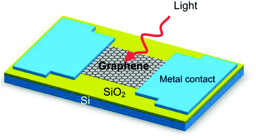 | ||
| Fig. 77 Scheme of a MGM photodetector. Adapted from ref. 995. | ||
The response time is ruled by μ. Graphene has huge μ, so it can be ultrafast.1428 Graphene's suitability for high-speed PDs was demonstrated in a communications link at 10 Gbit s−1 (ref. 1433).
In this section we summarize some key concepts as discussed in ref. 1434.
Many of the characteristics and unique capabilities of photodetection systems based on GRMs have been studied over the past few years, and a multitude of application areas have been addressed. Some of these have already reached a level of competitiveness with existing technologies. Various photodetection schemes and architectures have been proposed to date. The simplest configuration is the metal–graphene–metal (MGM) PD in which graphene is contacted with metal electrodes as source and drain.1429,1435,1436 Further, these PDs can be enhanced with plasmonic metal nanostructures,446 intrinsic plasmons,1437 p–n junctions in the graphene channel,1438,1439 and integration with waveguides,1318,1440,1441 and microcavities.1319,1442 Hybrid approaches employ semiconducting nano-particles, molecules, or plasmonic nano-systems as light absorbing materials, with graphene as the conduction channel, resulting in photoconductive-gain.1315,1443,1444 Devices have also been fabricated for detection of THz light,1445 where an antenna coupled to source and gate of the device excites plasma waves in the channel. Most importantly, graphene is compatible with the highly mature Si-based platform for electronics and photonics, making it a strong contender for low-cost and large-scale integration into optoelectronic networks and multi-pixel CMOS read-out circuits.
 . Here, A is the area of the photosensitive region, and BW is the frequency bandwidth of the detector. For sensitized photoconductors the external quantum efficiency is defined as QE = ηtransηabs, where ηtrans is the charge transfer efficiency and ηabs is the light absorption efficiency. A second important parameter is the lifetime, τtr, of the charge residing in the particles, as the light-induced change in carrier density Δn scales linearly with it: Δn = τtr × QE × ϕin. Photoconductive detectors are often benchmarked by their photoconductive gain, Gph = (Iph/q)/(ϕinQE), i.e. the number of detected charge carriers per single incident photon. This can be quantified by the ratio of the lifetime of the trapped carriers over the drift transit time, τtransit, of the SLG charge carriers from source to drain: Gph = τtr/τtransit. τtransit is governed by the applied field, thus it is shorter for higher bias and mobility: τtransit = L2/(μVbias), with L the source–drain separation distance.
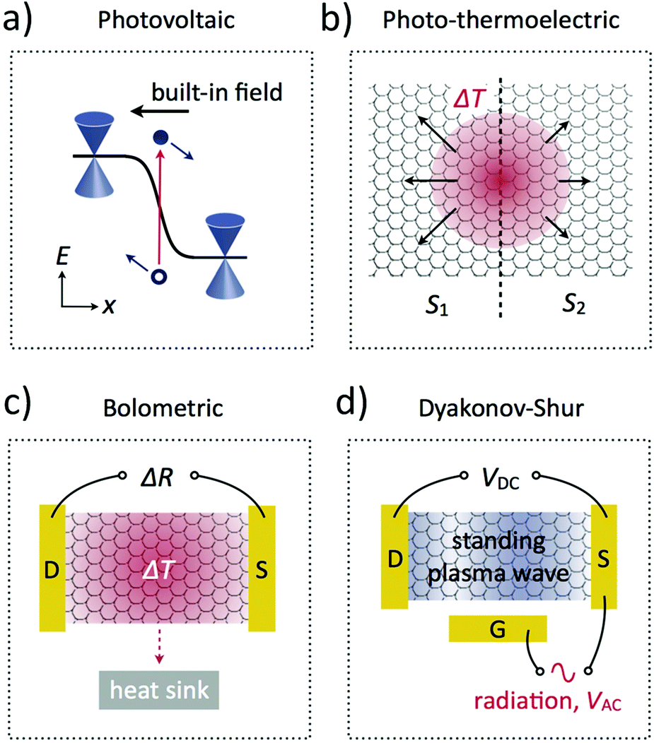 | ||
| Fig. 78 Schematic representation of the four different photocurrent generation mechanisms, (a) photovoltaic, (b) photothermoelectric, (c) bolometric and (d) plasma wave-assisted (Dyakonov–Shur). Adapted from ref. 1434. | ||
7.2.2.1. Photovoltaic effect. The photovoltaic photocurrent generation is based on the separation of photo-generated e–h pairs by built-in electric fields at junctions between negatively (n-type) and positively (p-type) doped regions of graphene or between differently-doped sections in general1430,1448,1449 (Fig. 78a). The same effect can be achieved by applying a source-drain bias voltage, producing an external electric field. However, this is generally avoided in the case of graphene, as it is a semi-metal, therefore generating a large dark current.
The doping that generates the built-in field can be introduced either by local chemical doping,1166 electrostatically, by the use of two (split) gates,1438,1448 or by taking advantage of the work-function difference between graphene and a contacting metal.1433,1448–1450 In the case of split gates, the doping can be tuned to be p or n, depending on the applied gate voltages, while in the case of graphene–metal junctions the doping in the contacted area is fixed. This is typically p-type for metals with a work function higher than the work function of intrinsic graphene (4.45 eV),1451 while the graphene channel can be p or n. The PV photocurrent direction depends only on the direction of the electric field, not on the overall doping level. Thus, it switches sign, when going from p–n to n–p, or from p–p+ to p+–p, where p+ means stronger p-type doping compared to p.
A lower bound on the intrinsic response time of SLG based MGM PDs was measured using an ultrafast optical correlation technique to be about 2 ps.1327 However, while the photogenerated carriers in graphene can have very high μ, the photodetection speed is not limited by the transit time of these carriers, but by the RC (resistance multiplied by capacitance) characteristics of the detector.23 Both response time and photo-detection efficiency depend on the ultrafast scattering processes. We note that e–e scattering513,1452,1453 can lead to the conversion of one high energy e–h pair into multiple e–h pairs of lower energy.512,1453,1454 This process, also denoted as carrier multiplication, can potentially enhance the overall photo-detection efficiency. Electron-phonon scattering,134,135,1455,1456 on the other hand, transfers electron energy to the phonons, which may lead to bolometric effects, as discussed in more detail below.
7.2.2.2. Photo-thermoelectric effect. Hot-carrier-assisted transport can play an important role in graphene1438,1439 (Fig. 78b). Due to the large optical phonon energy scale in this material208,1456 (∼200 meV), hot carriers created by the radiation field can remain at a temperature Te (and thus energy kBTe) higher than that of the lattice for many ps. Final equilibration of the hot electrons and the lattice occurs via the slower scattering between charge carriers and acoustic phonons.1457,1458 These processes take place on a ns timescale,1457 although they experience a substantial speed-up attributed to disorder-assisted collisions.1459–1461
The photo-generated hot electrons can produce a photovoltage VPTE by the photo-thermoelectric (PTE) effect (Seebeck effect): VPTE = (S2 − S1)ΔTeVPTE = (S2 − S1)ΔT, where S1,2 [V/K] is the thermoelectric power (Seebeck coefficient) in the two graphene regions with different doping, and ΔTe is the Te difference between the regions. More generically, the photovoltage VPTE can be calculated by integrating the local electric field which is generated by an optically-generated temperature gradient, dTe/dx, together with a spatially varying Seebeck coefficient: EPTE = ∫S·∇Tdx. The PTE effect has been shown to dominate in graphene p–n junctions1438,1439 or in suspended graphene.1462 Because hot electrons, rather than lattice heating, generate the electronic response under these conditions, PTE graphene detectors can achieve high bandwidths, as in the case of PV detectors. The thermoelectric power S (also called thermopower) is related to the electrical conductivity σ by the Mott formula:1463
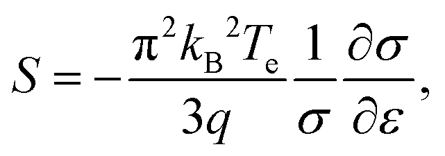 | (1) |
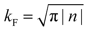 the Fermi wave vector, and n the carrier density. The Mott formula was derived utilizing the Sommerfeld expansion,1463 thus it is valid only for kBT ∝ εF. For this condition, S can be calculated from the transport characteristics of the device, i.e. from the dependence of conductance on gate voltage.
The sensitivity of PDs based on the PTE effect might be enhanced due to efficient intraband e–e scattering, leading to higher Te.1464,1465 A typical Rph ∼ 10−3 A W−1 was reported for PTE graphene PDs,31 similar to those of PV graphene PDs. However, higher Rph ∼ 10−2 A W−1, was observed in suspended TLG p–n junctions.1462 In this case, the interaction of substrate phonons with graphene electrons is inhibited, removing an important electron-phonon decay channel. This shows that electron/substrate polar phonon scattering can play a role, especially at RT, and removing it by suspending the graphene sheet can increase the hot electron temperature, and thus the photocurrent.
7.2.2.3. Bolometric effect. The bolometric effect is associated with the change in the transport conductance produced by heating associated with the incident photons (Fig. 78c). A bolometer measures the power of electromagnetic radiation by absorbing the incident radiation (dP) and reading out the resulting temperature increase dT.1446 Today, bolometers are mainly made of semiconductor1466 or superconductor absorptive materials,1446 and are widely used in the sub-millimeter (THz) wavelength range, where they are among the most sensitive detectors. The key parameters of a bolometer are the thermal resistance Rh = dT/dP, which ultimately defines its sensitivity, and the heat capacity Ch, which determines its response time τ = RhCh.1446 Graphene has small volume and low density of states, which results in low heat capacity Ch, thus a fast response. The cooling of electrons by acoustic phonons is inefficient, due to the small Fermi surface, and cooling by optical phonons requires very high Te (kBTe > 0.2 eV). Thus Rh is high giving rise to high bolometric sensitivity.
As this photodetection mechanism is based on a light-induced change in conductance instead of direct photocurrent generation, it requires an externally applied bias and can operate on homogeneous graphene, without the need to introduce a p–n junction. The conductance change induced by the incident light can be due to two mechanisms: (1) a change in the number of carriers contributing to the current; (2) a change in carrier mobility due to the associated temperature change. We note that (1) coincides with the photovoltaic effect, with the electric field generated by the external bias.
7.2.2.4. Photogating effect. The photogating process is associated to a light-induced change of the carrier density Δn of a conductor, therefore of its σ. For graphene, this change in σ is given by the relation: Δσ = Δn·e·μ.1434 Typically, the photogating effect starts with light absorption inside sensitizing centers in the vicinity of the GRM, such as nano-particles or molecules.1434 This absorption process leads to the generation of e–h pairs. Next, one type of charge carrier is transferred to the GRM (e.g. by an intrinsic electric field) while the other type of charge carrier resides in the particles, molecules or traps. As long as these charges are trapped, the other type of charges in the GRM sheet are re-circulated, due to the charge conservation condition. We note that the fundamental difference to the bolometric effect, which is based on the change in μ due to heating, is that the photogating effect is based on a light-induced change in n.
G ph can be strongly enhanced by using a high-μ conductor (such as graphene) and by a long τtr. At the same time, a long τtr reduces the operation speed. Therefore these detectors can be used for lower temporal bandwidth, such as video imaging applications. Photoconductive detectors may exhibit a high dark current, so a proper assessment of the detector performance is not just provided by the responsivity, but rather by measuring the NEP or D*.
7.2.2.5. Plasma-wave-assisted mechanism. Dyakonov and Shur (DS)1468,1469 proposed a photo-detection scheme, whereby a finite dc voltage is generated in response to an oscillating radiation field (Fig. 78d). This is based on the fact that a FET hosting a 2d electron gas can act as a cavity for plasma waves.1470 When these are weakly damped, i.e. when a plasma wave launched at the source can reach the drain in a time shorter than the momentum relaxation time τ, the detection of radiation exploits constructive interference of the plasma waves in the cavity, which results in a resonantly enhanced response. This is the so-called resonant regime of plasma-wave photodetection,1469 and can give rise to a signal that is 5–20 times stronger than the broadband non-resonant one. Broadband detection occurs when plasma waves are overdamped, i.e. when a plasma wave launched at the source decays before reaching the drain.1469
DS showed1469 that the photovoltage response of a 2d electron system in a FET, i.e. the electric potential difference between drain and source, contains a dc component even if the incoming field is ac, and thus provides rectification of the signal. This is particularly useful for the detection of THz radiation. Rectification occurs due to the non-linear response of the 2d electron gas in the FET channel and is unrelated to extrinsic rectification mechanisms due to e.g. Schottky barriers at contacts or other circuital elements that respond in a non-Ohmic manner. For the resonant regime, the dc photoresponse is characterized by peaks at odd multiples of the lowest plasma-wave frequency.1469 Resonant detection of THz radiation in graphene FET was theoretically discussed in ref. 1471 where the impact of hydrodynamic non-linearities strictly pertaining to the flow of the 2d electron gas in a graphene sheet was quantitatively addressed. Using the dispersion of plasma waves in graphene, it was concluded1471 that the typical linear device size required to operate in the THz spectral range varies in the interval ∼ 1–10 μm. RT THz detectors based on antenna-coupled GFETs, exploiting the DS mechanism have been demonstrated.1445,1472 In ref. 1445 the plasma waves excited by THz radiation were overdamped, thus the detectors did not operate in the resonant regime.77 The dependence of the photovoltage on carrier density in the FET channel displays also PTE contributions.1445,1472
| Description | Responsivity | Detector type | Bandwidth | Wavelength | IQE | EQE | Ref. |
|---|---|---|---|---|---|---|---|
| Graphene-metal junction | 6.1 mA W−1 | Photocurrent (PV/PTE) | >40 GHz | VIS, NIR | 10% | 0.5% | 1433,1479 |
| Graphene p–n junction | 10 mA W−1 | Photocurrent (PTE) | VIS | 35% | 2.5% | 1438,1439,1462 | |
| Graphene coupled to waveguide | 0.13 A W−1 | Photocurrent (PV/PTE) | >20 GHz | 1.3–2.75 μm | 10% | 10% | 1318,1440,1441 |
| Graphene-silicon heterojunction | 0.435 A W−1 | Schottky photodiode | 1 kHz | 0.2–1 μm | 65% | 1528 | |
| Biased graphene at RT | 0.2 mA W−1 | Bolometric | VIS, IR | 1450 | |||
| Dual-gated BLG at low temperature | 105 V W−1 | Bolometric | >1 GHz | 10 μm | 1492 | ||
| Hybrid graphene-QD | 108 A W−1 | Phototransistor | 100 Hz | 0.3–2 μm | ∼50% | 25% | 1315 |
| Graphene with THz-antenna | 1.2 V W−1 | Overdamped plasma waves | 1000 μm | 1472 | |||
| Graphene interdigitated THz antenna | 5 nA W−1 | Photovoltaic + photo-induced bolometric | ∼20 GHz | 2.5 THz | 1507 | ||
| SLG-TMD-SLG heterostructure | 0.1 A W−1 | Vertical photodiode | <650 nm | 30% | 1529,1530 | ||
| Biased MoS2 | 880 A W−1 | Photoconductor | 0.1 Hz | <700 nm | 1512 | ||
| Graphene double-layer heterostructure | >1 A W−1 | Phototransistor | 1 Hz | 0.5–3.2 μm | 1532 | ||
| WSe2 p–n junction | 16 mA W−1 | P–n photodiode | <750 nm | 60% | 3% | 1533–1535 | |
| GaS nanosheet | 19.1 A W−1 | Photoconductor | >10 Hz | 0.25–0.5 μm | 1536 |
A p–n junction is usually required to enhance the photoresponse. Such p–n junctions are often created close to the contacts, because of the difference in the work functions of metal and graphene,109,1478 or they can be created by local gates.1439 Responses at wavelengths of 0.514, 0.633, 1.5 and 2.4 μm have been reported.1433 Much broader spectral detection is expected because of the graphene ultra-wideband absorption. A GPD with a photoresponse of up to 40 GHz was reported.1479 The operating bandwidth is mainly limited by the time constant resulting from the device resistance, R, and capacitance, C. An RC-limited bandwidth ∼640 GHz was reported for graphene,1479 comparable to traditional photodetectors.1480 However, the maximum possible operating bandwidth is typically restricted by their transit time, the finite duration of the photogenerated current.1428 The transit-time-limited bandwidth could be >1500 GHz,1479 surpassing state-of-the-art PDs.
Although an external electric field can produce efficient photocurrent generation with an e–h separation efficiency >30%,1435 zero source–drain bias and dark current operations could be achieved by using the internal electric field formed near the metal electrode–graphene interfaces.1433,1480 However, the small effective area of the internal electric field could decrease the detection efficiency,1433,1480 as most of the generated e–h pairs would be out of the electric field, thus recombining, rather than being separated. The internal photocurrent efficiencies (15–30%1435) and external responsivities (generated electric current for a given input optical power) of ∼6 mA W−1 reported for basic GPDs with two contacts1433 are relatively low compared with existing PDs.1428 This is mainly due to limited optical absorption when only one SLG is used, short photocarrier lifetimes512 and small effective photodetection areas (∼200 nm (ref. 1479)). To date, responsivities ∼0.1 A W−1 for ultrafast waveguide integrated GPDs have been reported,1316–1318 while high-gain hybrid graphene/QD PDs have revealed responsivities up to 108 A W−1.1315 In order to achieve these high responsivities, it is important to optimize light absorption within the narrow regions around the interfaces or to absorb light in a different material.
One target is to increase the light absorption of graphene, and address the difficulty of extracting photoelectrons (only a small area of the p–n junction contributes to current generation), as well as addressing the absence of a photocurrent for the condition of uniform flood illumination on both contacts of the device. Unless the contacts are made of different materials, the voltage/current produced at both contacts will be of opposite polarity for symmetry reasons, resulting in zero net signal.1429,1433,1435
The optimization of the contacts needs to be pursued both theoretically and experimentally. Other possible ways of overcoming these restrictions comprise the use of plasmonic nanostructures placed near the contacts.446 Incident light, absorbed by such nanostructures, can be converted into plasmonic oscillations, with an enhancement of the local electric field.446 Such field enhancement, exactly in the area of the p–n junction formed in graphene, can result in a significant performance improvement. The role of the plasmonic nanostructures is to guide the incident electromagnetic energy directly to the p–n junction.
Nanostructures with geometries resonant at desired wavelengths need to be investigated for selective amplification, potentially allowing light filtering and detection, as well as polarization determination in a single device at high frequencies. The frequency performance can even be improved in comparison with traditional devices, as the plasmonic structures add only negligible contribution to the capacitance (fractions of fFs), but can significantly reduce contact resistance. Further optimization (e.g., making use of coupled or cascaded plasmon resonances1481,1482) could increase the photovoltage enhancement.
The advances in the fabrication of sandwich structures can help elucidate the process of light absorption and charge separation in vertical stacks, optimizing efficient light conversion into electricity. Composite 3d structures could be realized with some layers nanostructured, so to manipulate the working range of the device.
The low optical absorption and the narrow photocurrent generation region do not impose serious restrictions on the usability of graphene for photodetection. A number of concepts can be pursued to overcome these issues, and responsivities comparable to those of semiconductor-based devices can be reached. However, graphene's constant optical absorption over a broad spectral range allows light detection over a wavelength range superior to any other material.
The photothermoelectric effect, which exploits the conversion of photon energy into heat and then electric signal,1428 may play an important part in photocurrent generation in graphene devices.1435,1476 In particular, photocurrents assisted by hot-carriers are enhanced in the vicinity of pn-junctions leading to strongly enhanced responsivities.1439 The efficiency of hot-carrier generation depends on the competition of different relaxation pathways and can be greatly enhanced when photoexcited carriers do not lose energy as heat, but instead transfer their excess energy into the production of additional hot carriers or e–h pairs via carrier–carrier scattering. Pump-probe measurements have shown that in graphene the latter process is very efficient.512,513,1464 These results indicate that the production of secondary e–h pairs dominates the ultrafast energy relaxation of photoexcited carriers, prevailing over optical phonon emission in a wide range of photon wavelengths.1464 This leads to the production of secondary hot electrons, originating from the conduction band. As hot electrons in graphene can drive currents, multiple hot-carrier generation makes graphene promising for highly efficient broadband extraction of light energy into electronic degrees of freedom, enabling high-efficiency optoelectronic applications. Employing these unique properties, the development of novel designs for further optimization of thermoelectric light harvesting and detection may be possible. In particular, the efficient conversion from photons to hot carriers, a unique aspect of graphene due to the absence of a bandgap and strong carrier–carrier interactions, should be exploited.
Another approach to increase the responsivity is to integrate a GPD a highly confined optical waveguide and increase the optical absorption, Fig. 79.1316–1318 NIR light is coupled to a Si waveguide, which is embedded in SiO2. A graphene sheet is located on top of the Si waveguide and there is a thin isolation oxide layer in-between. The fundamental TM (transverse magnetic) mode would get almost completely absorbed in the graphene, as the light propagates along the waveguide. The local field gradient at the metal/graphene interface drives a photocurrent towards the ground leads. The metal electrodes may also be replaced by poly-Si to reduce optical mode damping. The expected foot-print of such device is ∼30 μm2, comparable to state-of-the-art Ge PDs, nowadays used in highly-integrated Si photonics for on-chip interconnects. The simple device geometry, less complex processing and compatibility with Si technology could make graphene an alternative to other semiconductors such as Ge, even for large-scale integrated photonics. Apart from its superior physical properties, graphene's strength is its 2d character, which makes it compatible with standard semiconductor technology and allows for monolithic or hybrid integration with other materials. Graphene sheets can be transferred to arbitrary substrates (including flexible), etched into any shape, integrated with waveguides or cavities, electrically contacted, etc.
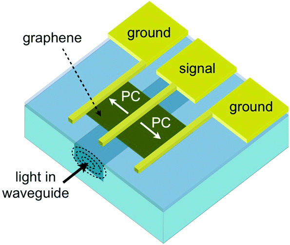 | ||
| Fig. 79 Schematic of an integrated waveguide GPD. | ||
All these aspects lead us to consider graphene as a promising new material for photonic integrated circuits,1483 particularly for high data-rate optical interconnects. Graphene will allow the realization of high-speed, compact-footprint PDs integrated with Si waveguides or plasmonic circuits. The mechanical flexibility of graphene may also enable the integration with bendable substrates and low-cost plastic waveguides. Photonic integrated circuits are based on the convergence and co-integration of passive optical components (waveguides, (de-)multiplexers, filters, etc.) with modulators, switches and PDs. State-of-the-art monolithic PDs are based on Ge or III–V semiconductors, but their responsivity ranges are spectrally limited. Graphene, without such a limit due to the gapless dispersion of the Dirac electrons, could thus pave the way for broadband photodetection, from the O-band (1260–1360 nm) to the U-band (1625–1675 nm), and beyond (e.g. 850 nm). The expected foot-prints of the devices are even smaller than those of state-of-the-art Ge devices used in Si photonics. The simple device geometry, less complex processing, compatibility with CMOS technology, and broadband and ultra-fast operation could make graphene an alternative to other materials, even for large-scale integrated photonics.
The 2d character of graphene and the possibility of large-area fabrication allows up-scaling from single devices into arrays. This could enable a pixelated, camera-like structure, where each pixel may be read out individually. Co-integration with Si transistors as amplifying elements is envisaged. The goal is to achieve gated PD arrays with strongly enhanced responsivity. The energy spectrum and optical properties of graphene can be modified through an electrostatic field. This can be utilized to realize a waveguide-integrated electro-optical modulators at 1550 nm, based on optical absorption for photon energies 2EF < Eph (Eph is the photon energy, EF denotes the Fermi energy) and absorption suppression for 2EF > Eph due to Pauli blocking.1339 Graphene-based modulators can be realized on a much smaller foot-print than devices using semiconductor materials for electro-absorption or electro-refraction by the Pockels, Kerr1484 and Franz–Keldysh effects.1485,1486
Another target will be the integration of graphene electro-absorption modulators into Si waveguide ring resonators and Fabry–Perot cavities with grating mirrors, to further decrease the foot-print. This will lead to higher modulation depth and speed than previously reported.
When it comes to high-demand applications, requiring photon detection at very low levels, even approaching single photon detection, photodiodes cannot be chosen, because their quantum efficiency is limited to unity, accounting for 1 carrier per photon. Therefore, the electrical signal suffers from read-out electronic noise, which overwhelms the photocurrent at low intensities. In view of this constraint, gain has been sought in PDs: a mechanism that can provide multiple electrical carriers per single incident photon.
Photoconductive detectors are based on the effect of carrier recirculation,1315 providing Ohmic contacts to the semiconductor and appropriate sensitizing centres that can prolong the carrier lifetime. Photoconductive gain is then possible, with a value given by the ratio of the carrier lifetime over the transit time. Photoconductive detectors have regained attention with the advent of colloidal QDs PDs.1487 Photoconductive gain ∼103–105 was reported for PbS, ZnO or CdSe QDs,1487–1489 limited, however, by the low μ of QD films. Phototransistors have also been proposed to provide for photoconductive gain.1488 A FET-like phototransistor was reported with single-photon counting potential, based on a 2DEG channel and QDs as the photosensitive gate, in an epitaxially grown structure. The 2DEG was formed in an AlGaAs substrate by cooling the device to 4 K and it was critical in achieving high sensitivity due to the high μ that can be achieved in a 2DEG.
Graphene is an excellent candidate for high-gain PDs because of the high μ, and since it is 2d. Thus, its conductance is very sensitive to electrostatic perturbation by photogenerated carriers close to the surface. This makes it a particularly promising material for high gain PDs by photogating. Additionally, graphene is a very thin, flexible and durable, and can be fabricated in a large scale and easily deposited on Si, offering integration into standard ICs. Thus, the demonstration of photodetection gain with graphene would be the basis for a plethora of applications, such as integrated optoelectronic circuits, biomedical imaging, remote sensing, optical communications, and quantum information technology.
Ultra-sensitive PDs and image sensor arrays for visible and IR imaging have been developed,1315 based on sensitized graphene: a film of semiconducting particles or QDs is deposited on the graphene sheet,1315 see Fig. 80. Colloidal QDs offer high absorption and bandgap tuneability from UV to SWIR,1488 and could be employed as a vehicle to demonstrate the potential of this technology. Through sensitization, strong absorption ∼50–100% can be achieved.1315 The detection mechanism is based on photogating,1490 where light induced trapped charges in the QD change the resistance of graphene. The photoconductive gain associated to this mechanism can be quantified by the ratio of the lifetime of the trapped carriers in the QD over the drift time of the charge carriers in graphene. A photoconductive gain ∼108 and responsivity ∼107 A W−1 can be achieved,1315 thanks to the high μ of the graphene channel, and the long carrier lifetime of the photogenerated carriers in the QD layer.1315 In combination with the high quantum efficiency >25% and low noise-equivalent-power ∼10−17 W, this hybrid QD-GPD is an excellent platform for large-scale sensitive SWIR detection.
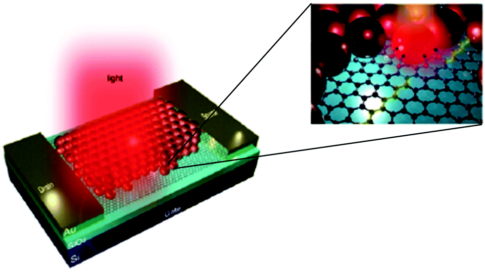 | ||
| Fig. 80 Schematic of GQD hybrid phototransistor, in which a graphene flake is deposited onto Si/SiO2 coated with PbS QDs. Incident photons create e–h pairs in the PbS QDs. [Adapted from ref. 1315]. | ||
Research needs to be extended to the mid-IR, targeting broadband detection in the wavelength range 3–30 μm. Surface plasmon nanostructures functioning as optical antennas1491 could be used to couple the long-wavelength radiation to the graphene sheets. In the simplest case, a bow-tie antenna concentrates the radiation energy to a confined region of sub-wavelength dimension.1445 Asymmetric contacts1433 or, alternatively, a potential gradient produced by band profile engineering can be used to separate the carriers. Antenna arrays will allow scaling the device dimensions to large areas. Due to the long wavelength of the radiation, the lithography requirements are relaxed, which will allow cm2-sized detector arrays/cameras by optical lithography. More advanced plasmonic geometries may be used to further concentrate the radiation at the metal/graphene interfaces.
7.2.3.1. Bolometers. Bolometric responses have been measured on a biased graphene sheet at RT.1437,1492Ref. 1437 reported that two mechanisms result in bolometric photocurrents with opposite sign. Namely, the T dependence of μ leads to a reduction of the conductance, while photo-induced excess carriers induce an enhancement of the conductance. By changing EF in graphene, one can control which mechanism dominates.1437 Near the Dirac point, where the carrier density is lowest, PV effects dominate, while far away PTE effects dominate.1437
The relative contributions of the two mechanisms depend on the nature of the device, such as the presence and nature of the substrate (i.e. polar versus non-polar), the quality of the sample, as expressed by μ, and the experimental conditions, such as the magnitude of applied bias and T. E.g., it was shown1450 that in a partially supported (on SiO2) and partially suspended sample, thermal effects dominate in the suspended part, and photovoltaic effects the supported one.
The weak T dependence of the electrical resistance in graphene,1493 however, imposes a major challenge for reading dT through electrical transport measurements, and for this reason a small responsivity of 0.2 mA W−1 was measured for RT graphene bolometric detectors.1437 To solve this problem, a dual-gated BLG device with optically transparent top gate was used1492 to open a band gap at the Dirac point127,1145 and obtain Te-dependent resistance.127 The device was measured under MIR illumination (10.6 μm) using a four-terminal configuration, and the photoresponse was identified to be bolometric.1492 The thermal resistance had a R ∝ T−3.45 dependence, which approximately agrees with the theoretically expected T−3 dependence for (disorder-free) phonon cooling.1494,1495 The detector exhibits excellent performance: NEP ∼33 fW per √Hz at T = 5 K (several times lower than commercial Si or superconducting bolometers) and an intrinsic bandwidth >1 GHz (3–5 orders of magnitude higher). Another approach for implementing a T-dependent graphene resistance is to drive the electronic system into the strong localization regime by adding disorder. This was achieved at low T by using defective graphene films.1496
Ref. 1497 reported a graphene-superconductor tunnel junction bolometer. When biased within the superconducting gap, the junction resistance is dominated by tunnelling of the thermally excited quasi-particles. The increase of Te in graphene under illumination decreases the tunnelling resistance, which can be probed by a small DC current. For DC signals, the contacts are highly resistive due to the superconducting gap, whereas for high-frequency (RF to optical frequencies) signals, the contact has low impedance due to the contact capacitance, therefore the graphene resistance can be matched with that of an antenna. Although the device in ref. 1497 was measured with RF waves, the concept can also be applied for optical detection, see ref. 1498 for a recent review.
7.2.3.2. Long-wavelength photodetectors. Applications of long-wavelength radiation are manifold. The term “long-wavelength” is used to refer to the FIR (THz) and MIR, i.e. the wavelength range 3–1000 μm. Many chemical agents, explosives or narcotics feature spectral fingerprints in this range.1499 Optoelectronic devices operating in the THz and MIR may be employed in homeland-security-related applications, e.g. in security systems at airports monitoring dangerous substances, but also in environmental-related applications, e.g. gas spectrometers for air-quality control, whereby traces of threat chemicals have to be detected against a spectral background. At the same time, the MIR spectral range is as well fairly unexploited, with many interesting imaging and sensing applications in medicine and security.1500
The most sensitive detectors of THz radiation require deep cryogenic cooling: superconducting hot-electron bolometers1501 reach NEPs as low as a few fw/Hz1/2 (ref. 1501) with modulation bandwidths up to the GHz.1501 On the other hand, RT THz detectors are either not very sensitive,1501 or extremely slow,1501 or operate well only below 1 THz.1501
The situation becomes even more complex when technologies that can be produced into matrix arrays are considered. Commercial THz or MIR FPAs are based on microbolometer elements, and provide moderate sensitivities and response speeds (NEPs of few pW/Hz1/2 per pixel and ∼1 kHz bandwidth near 1 THz1501). Recently, Fast electronic devices, based on the gate-modulation of the conductance channel by the incoming radiation (often called plasma-wave detectors1469,1502,1503), have been realized in both HEMT1504 and CMOS1505 architectures and show NEPs already competitive with microbolometers and response times up to the MHz range.1554 This technology is also scalable to even larger arrays (a 1024 pixel camera was demonstrated at 0.7 THz1506). For what concerns the mid-IR, narrow-gap semiconductors, currently used in photodiode detectors, still suffer from serious problems in controlling the material quality and poor integration capabilities.
GFETs can be exploited to considerably advance the present state-of-the-art of plasma-wave detectors, see Fig. 81 (ref. 1445), taking advantage of the high μ.1445 This would allow improved performance in terms of responsivity and bandwidth, and operation limits well above 1 THz. Even more appealing is the possibility to reach a regime in which stationary plasma modes are excited in the transistor channel, leading to resonant, gate tuneable, enhancement of the responsivity. This also means that the detected radiation wavelength can be controlled by the gate voltage, hence leading to a novel passive spectroscopy system, which is presently not available in the THz.1472
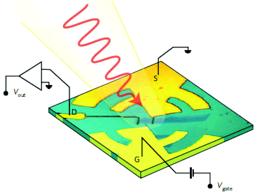 | ||
| Fig. 81 Antenna-coupled GFET-terahertz detector. The terahertz radiation is focused by off-axis parabolic mirrors. Adapted from ref. 1445. | ||
Graphene-based broadband THz detectors working at RT were shown1507 with Rv ∼ 5 nA W−1 and fast response rise times (∼50 ps) at 2.5 THz, which makes them already suitable for timing applications. The device employed a log-periodic THz antenna,1507 with a central interdigitated comb providing the electrical contact to the SLG.
PTE graphene THz detectors, operating at 2.5 THz and based on exfoliated SLG with a pattern of asymmetric metal contacts were also reported.1508 In ref. 1508, the generated photoexcited carriers rapidly thermalized due to the strong electron–electron interactions, while losing energy to the lattice more slowly. The Te gradient drives electron diffusion, and asymmetry, due to dissimilar contact metals, produces a net current via the PTE.
Finally, with the development of large-area growth techniques, multi-pixel camera-like arrays are feasible and potentially relatively low-cost. The long-term objective is the realization of a graphene THz camera capable of performing passive imaging and providing spectroscopic information.
7.2.3.3. 2d crystals and hybrids. Although the bulk properties of layered TMDs have been investigated for many decades,111 their 2d forms have recently attracted much attention due to their potential applications in optoelectronics.1509 The properties of TMDs depend on N. E.g., MoS2 has a bulk indirect band gap of 1.3 eV, which becomes a direct band gap of ∼1.8 eV in 1L-MoS2.1510 This changes the optical properties, such as absorption spectrum and PL. Ref. 378 showed a 1000-fold enhancement of the luminescence quantum yield for 1L compared to bulk MoS2. Valley polarization controlled by optical pumping was also demonstrated in 1L-MoS2,1310 and polarization was maintained for longer than 1 ns.1511
Compared to classical direct band gap semiconductors, TMDs can also offer additional advantages in the context of optoelectronics because of their transparency, mechanical flexibility and easy processing. This suggests the possibility of photovoltaic and photodetection applications in MoS2 and other semiconducting TMDs. PDs made of 1L-MoS2 displayed high external photoresponsivity, i.e. the measure of the electrical output per optical input, (over 880 A W−1 at 561 nm1512) and a stable photoswitching time of 50 ms.1513 Moreover, the ability to tune the bandgap by varying N allows the detection of light at different wavelengths.1514 The strong photothermoelectric effect measured at metal-MoS2 junctions1515 can also be useful for applications in thermopower generation.1515
One important use of layered semiconductors such as MoS2 could be in making novel heterojunction devices. E.g., a metal–semiconductor–metal heterojunction photodetector, made of MoS2 and amorphous silicon (a-Si), with rise and fall times ∼0.3 ms was demonstrated.1516 The transient response of MoS2/a-Si hybrid PD does not show persistent (residual) photoconductivity, thus making this heterojunction roughly 10 times faster with respect to a-Si devices.1516,1517 A photoresponsivity ∼210 mA W−1 was measured for green light, the wavelength used in commercial imaging systems, which is 2–4 times larger than that of a-Si.
MoS2 is a good illustration of the wide range of optical properties offered by 2d crystals. These complement those of graphene in many ways: graphene is useful for broadband, ultrafast technologies, whereas semiconducting TMDs are advantageous for applications requiring strong light absorption1529 and electroluminescence.1518 A promising approach to combine these properties and create multi-functional, high performance materials consists of assembling graphene with other 2d crystals in heterogeneous stacks and hybrid devices.1519 This new device architecture has lead to novel transistor concepts based on vertical transport between two graphene electrodes, separated by h-BN, MoS2 or WS2 layers.106,1520,1529 The same hybrid devices have shown potential for photovoltaic applications with a photoresponsivity above 0.1 A W−1 and EQE >30%.1529 Graphene layers can be used as work-function tuneable electrodes,1529 while TMDs may be employed as photoactive material,1529 displaying a strong light–matter interaction and photon absorption. E–h pairs may be created in the TMD and separated between the two neighbouring graphene layers, exploiting the whole graphene/TMD junction surface to produce photocurrent.1529
The fact that charge carriers in monolayer dichalcogenides behave as spin–valley coupled massive Dirac fermions,1521 gives the possibility of building optoelectronic devices exploiting the valley degree of freedom. The valley index is expected to be robust against scattering by smooth deformations and long-wavelength phonons.1522 In monolayers of group-VI semiconducting dichalcogenides (MoS2, MoSe2, WS2 and WSe2), the inversion symmetry is broken, Fig. 82a. Together with the large mass of the constituent elements and 2d confinement, this results in strong spin–orbit coupling, valence band splitting1523 and spin–valley coupling,1522Fig. 82b. The valence band splitting ranges between 0.15 eV for MoS2 to 0.465 eV for WSe2 which is composed of heavier atoms.1523 The flipping of the valley index is expected to require atomic scale scatterers. In the valence band, because of the large spin-splitting which is opposite for different valleys, this will require atomic scale magnetic scatterers. This implies that the valley index, once valley polarization in the material is established, will be very robust. Experimental demonstrations of such valley selection were reported.1310Ref. 1310 used optical excitation with circularly polarized light to control the carrier populations in different valleys. These couplings between spin, orbit and valley degrees of freedom distinguish monolayer dichalcogenides from other semiconductors and graphene and could result in new, as yet unforeseen applications.
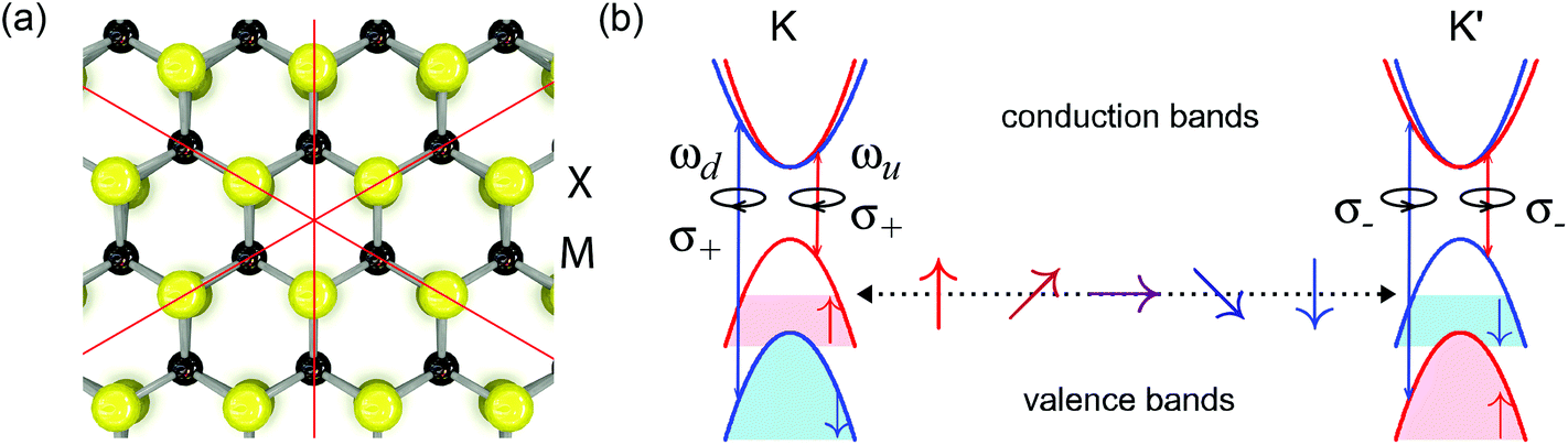 | ||
| Fig. 82 (a) Top view of the lattice of 1L-MX2. The structure has no inversion symmetry. (b) Low-energy band structures of 1L-MX2 for the K and K′ valleys. The bottom of the conduction band is degenerate while the valence band is split into spin-up and spin down states. Intervalley scattering can occur only simultaneously with spin-flipping, requiring atomic scale magnetic scatterers. Vertical arrows show optical selection rules. For a given Fermi level, different excitation frequencies can be used to select between spin states, while the valley can be controlled with circular polarization. [Adapted from ref. 1521]. | ||
The coupled spin, charge and valley degrees of freedom may also result in spin, charge and valley-Hall effects. E.g., excitation with circular polarizations could generate Hall current, detected as voltage across the edges of the sample.1531 Linearly polarized light on the other hand would result in pure spin and valley currents in the absence of charge currents. Such demonstration of pure valley current would be the next step in demonstrating valleytronic devices.
High-speed applications. High-speed photodetection superior to existing technologies is desirable for optical communications applications. The current bandwidth of graphene-based PDs was measured to be 262 GHz.1327 Due to the broadband absorption of graphene, photoresponsivity for visible, NIR and SWIR light was shown to be fairly constant (up to ∼3 μm1524), with Rph up to ∼0.13 A W−1, exploiting integration with waveguides1316,1318 or enhancements by plasmonics.446 In terms of bandwidth, graphene is thus capable of outperforming other technologies being investigated for optical communications, such as monolithically integrated Ge.1525,1526 High-speed PDs were also realized with III–V semiconductors (>300 GHz),1527 but these are difficult to integrate with Si optical and electronic technologies. An outstanding challenge for graphene-based PDs remains the increase of responsivity and effective detection area. Heterostructure stacks of 2d materials for vertical photocurrent extraction have large detection areas1529 and may therefore address the latter issue. An additional distinct advantage compared to existing technologies is that graphene is a platform for high-speed light modulation and detection on the same chip. While the individual elements have been realized, the integration of an all-optical link and the implementation of large-scale circuitry remains an outstanding challenge.
Highly sensitive detection. High sensitivity photo-detection has become a major functionality for a plethora of applications, such as remote sensing, biomedical imaging, optical communications, gas sensing etc. For the vast majority of applications, such as digital imaging and metrology, Si photodiodes exhibit excellent performance and are cost-effective due to their ease of integration with CMOS electronics. For applications where transparency and flexibility is important GRM-based photodiodes represent a promising alternative. For applications where detection of SWIR to MIR is required, Si is not a suitable absorber, and III–V semiconductors offer an alternative, but they are costly and difficult to integrate with Si read-out electronics. In this case, GRM-based photodiodes, photoconductors and hybrid phototransistors are particularly promising because they exhibit high photoconductive gain due to the high mobility of GRMs, do not require high voltages, and can be monolithically integrated with existing Si-based multi-pixel focal-plane arrays.1315,1443,1444,1537 By sensitizing the GRM with QDs, the sensitivity range can cover UV-visible,1538,1539 as well as SWIR1487 and MIR.1540 The outstanding challenge of this type of photoconductive detectors is the dark current, which can be addressed by the read-out circuitry (similar to bolometric systems). The reported projected NEP (∼10−17 W) and specific detectivity D* (7 × 10¹³ Jones)1315 are on par with existing technologies, such as InGaAs. Outstanding challenges include improvement in speed (currently up to 100 Hz), large-scale production and integration of multi-pixel arrays. Alternatively, p–n photodiode-based TMDs exhibit high sensitivity (see e.g.ref. 1534, 1535) and low dark current. Outstanding challenges include the improvement of the sensitive area and large-scale production.
Mid-infrared detection. The detection of MIR light is important for bio-sensing, security, thermal imaging, etc. For this frequency range, graphene can offer an appealing advantage compared to other materials, by employing plasmons, which resonantly enhance absorption for a wavelength that is tunable by a gate, offering in situ tunable spectral selectivity. The major outstanding challenge for this wavelength range is the carrier extraction, e.g. by utilizing p–n junctions in lateral or vertical structures, or by employing bolometric detection. Graphene bolometers have shown excellent performance1492 at low temperature, with NEP ∼ 33 fW per √Hz, comparable to existing technologies. The main challenge remains the matching of the high graphene impedance (tens of kΩ) to that of free space (377 Ω) for efficient photon coupling.
Terahertz detection. Photodetection of FIR radiation is significant for a variety of applications, ranging from medical diagnostics to process control, homeland security and cultural heritage. Commercially available THz detectors are based on thermal sensing elements that are either very slow (10–400 Hz modulation and NEP ∼ 10−10 W per √Hz) or require deep cryogenic cooling (4 K for superconducting hot-electron bolometers), while those exploiting fast nonlinear electronics (Schottky diodes) or high-mobility transistors are usually limited to sub-THz frequencies.1541 Graphene can exceed these limits by exploiting THz plasma waves that are weakly damped in high-quality samples, allowing for resonant detection regimes in a FET. This could potentially beat all other technologies at RT, but a major challenge is the demonstration of the resonant DS detection mechanism1468,1469 by integrating high-mobility graphene with appropriate THz antennas. However, graphene THz detectors have already been demonstrated for the range 0.29–0.38 THz with a NEP ∼ 10−9 W per √Hz,1445 and for the range 2 THz with a NEP ∼ 10−8 W per √Hz.1508 The combination of scalability at higher frequencies, the prospects for integration with Si-platforms as well as the potential for implementing flexible devices, makes graphene highly competitive for a future generation of THz detection systems.
Although photodetection platforms based on GRMs have been developed for a wide variety of applications at a remarkable pace, outstanding challenges remain to demonstrate the true potential and to exploit the distinct advantages of 2d crystals. The prospects for commercialization will not just depend on the detector performance, but likely also on some of the distinct advantages and capabilities, in addition to the ability to realize production of large-scale high-quality 2d materials at a low-cost, and to establish large-scale integration with existing photonic and electronic platforms, such as CMOS technologies.
7.3. Graphene plasmonics
Photonic technologies, based on light–matter interactions, already have a significant slice of today's markets.1542 With the advent of nanofabrication, light–matter interactions can now be studied and tailored at a fundamental level. Of recent interest is the use of metallic nanoparticles (MNPs), where surface plasmon resonances (SPRs) greatly enhance light–matter interactions.1543 SPRs are characterized by a large extinction cross section and the electromagnetic field is amplified by several orders of magnitude nearby the resonant MNPs.1543 Because of the near-field focusing at the SPR, every photoelectrical activity, such as absorption and emission, gets enhanced on the MNP surface. At high enough intensity, these two effects get coupled in a nonlinear manner exhibiting novel phenomena. Plasmon resonances can be tuned by acting on the shape654 and on the mutual interactions of the MNPs.1544 The dynamics of the plasmon resonance is extremely fast: ∼10 fs for plasmon dephasing,1545 ∼100 fs for equilibration into a hot electron distribution via e–e scattering1545 and ∼1 ps for relaxation via phonon emission.1545 Plasmonic nanostructures are usually characterized by good thermal1546,1547 and chemical stability1548,1549 and can be functionalized by chemical reactions on the surface.1550,1551 Finally, the noble metals are excellent electrical conductors.1552The combinations of semiconductor quantum dots (SQD) with MNPs1553 allows the study of the strong coupling regime, in which there is reversible exchange of energy between the emitter and the MNP (cavity) mode, giving rise to mixed light–matter cavity-polariton modes.1553 This mode, the physics of which is most conveniently described by a combination of classical and quantum mechanics,1553 has possible applications in a broad range of fields, including quantum information, interfacing of electronic and photonic components, surface plasmon lasers, solar energy harvesting, sensors and actuators. Over the past few years, hybrid SQD-MNP structures were manufactured in order to combine the discrete excitonic response with the strong optical response of plasmons.1554 In these structures, long-range Coulomb interaction couples the two subsystems creating hybrid exciton-plasmon excitations, resulting into Förster energy transfer,1555 Rabi charge oscillations,1556 nonlinear Fano resonances1554 and bistability.1557 Surface plasmon amplification by stimulated emission of radiation, where, rather than amplifying light in a conventional laser cavity, a plasmonic ‘spacer’ amplifies it with the help of plasmons, was used to develop nanolasers.1558
Graphene is poised to make a significant impact in modern photonics. A large part of this will be enabled by the advent of plasmonics to enhance and facilitate light–matter interactions. Recent work has shown the benefit of MNP in graphene-based photonic applications, such as graphene PVs446 and SERS.1333 Intrinsic graphene plasmons provide a suitable alternative to noble-metal plasmons due to their much larger confinement1313 and long propagation distances,1313 with the advantage of being tuneable via electrostatic gating.1313,1321 Compared to conventional plasmonic metals, graphene can lead to much larger field enhancements and optical field confinement.1313
Graphene-MNP-SQD complexes might play an important role in future optoelectronic and quantum information technologies. The target is to develop hybrid graphene-plasmonic devices with higher performance than non-hybrid devices. The interaction between graphene nanodisks or ribbons with metallic nanostructures can be exploited for the realization of optical switches and single photon devices,1559 taking advantage of GSA and the local electromagnetic field amplification induced by localized surface plasmons. Such hybrids are promising candidates for the realization of nano-optical devices, such as ultrafast nano-optical switches, surface Plasmon-polariton amplifiers, lasers, IR detectors, single-photon quantum devices, and ultrasensitive detectors. Enhancement of energy transfer is also important in solar energy applications, such as in DSSCs, where facilitation of dye–MNP interactions may play an important role in improving performance. Graphene can be made luminescent,689 thus its interaction with MNPs can be exploited to enhance and tailor its emission properties.
Sensitive photodetection in the SWIR would enable passive night vision1560,1561 from 1 to 1.7 μm, and biomedical imaging for tumour detection,1562 exploiting the tissue transparent windows around 900 and 1100 nm.1563,1564 Additional application are astrophysics,1565 remote sensing for climate and natural resources monitoring,1566 food and pharmaceutical industries for quality control and product inspection1567 and identification.1568
Modelling of the optical properties, such as extinction, absorption, and scattering cross-sections, as well as local field enhancement in the proximity of metallic nanostructures due to plasmon resonances1569 is important, in order to predict their functions and to engineer their properties. It is thus necessary to achieve a thorough understanding of the interaction between the subsystems and how their individual optical properties contribute to the formation of novel effects. Advanced computer models for the optical response of the constituent subsystems, incorporating both photonic and electronic degrees of freedom in a direct time-domain semi-classical approach are needed. Finite element methods such as the Discrete Dipole Approximation (DDA)1570 and time domain methods, such as the Finite-Difference Time-Domain (FDTD),1571 represent some of the most effective and versatile solutions for modelling the optical properties of nanostructures with complex form and hybrid composition.
Another important issue that needs to be addressed is the response of molecules or SQD that are very close to the MNP or graphene surface, due to the nonlocal response of the metal and graphene dielectric functions. This may have an important role on the actual field enhancement and energy transfer rates. An explicit scheme for taking into account spontaneous emission also needs to be implemented. Such a rich model inventory to describe graphene, metals and active materials will enable the detailed time-resolved simulation of novel graphene-based photonic and plasmonic devices. This modelling capability will facilitate the design of future graphene-based photonic and plasmonic applications.
The large-scale realization of hybrid devices will require versatile preparation techniques with high control on the surface of metal nanostructures. In some cases, a high degree of purity will be required for the metal–graphene contacts, while in other cases the ability to self-assemble the metal and graphene components will be needed. This could achieved via the insertion of appropriate synthetic mediators, such as molecules anchored on the surface of plasmonic nanostructures. The control of the surface of the plasmonic nanostructures will play a key role in the realization of hybrid devices. Some devices will require ultra-clean interfaces between graphene and metal nanostructures, which can only be obtained through ultra-clean chemical free techniques of synthesis. In other cases, the creation of ordered structures on a large scale may be achieved through self-assembly of plasmonic nanostructures and graphene, which can be guided by an intermediate molecule, eventually bound to the surface of metal nanostructures by exploiting the surface chemistry of noble metals.1572 Laser ablation synthesis in solution of plasmonic nanostructures has the potential for fulfilling a large part of the above requirements.654,1573
Graphene can be combined with plasmonic metamaterials.1574 This promises more effective conversion of light into electricity,446 extremely sensitive sensors based on optical transduction1575 and a possibility to realize materials with optical properties that could be governed by the graphene gating, often referred to as active plasmonics.1576 Challenges in combining plasmonics with graphene include control of doping, and problems with graphene gating caused by the presence of the plasmonic metamaterial. Small, fast and cheap optical modulators based on graphene-based plasmonic metamaterials could be used in optoelectronics to enhance the speed of internet. More efficient photocells which make use of a larger part of the solar spectrum and produce more electricity under the same illumination. Extremely sensitive optical plasmonic nanosensors coupled with graphene could push forward optical transduction methods.
Besides the tight confinement, GSPs exhibit relatively long propagation distances as compared to SP modes in noble metals.1321 This was confirmed in ref. 252, 1326, 1577 which showed a factor of three enhancement of the plasmon lifetime. At least another factor 100 improvement could achieved by optimizing the substrate material and increasing μ of graphene.
Furthermore, the frequencies of SPP modes are highly tuneable via electrostatic gating.252,1326 This property can be used to direct plasmons along switchable paths controlled by electrostatic gates, representing a unique capability not present in metals. The versatility of graphene means that graphene-based plasmonics may enable novel optical devices working in different frequency ranges, from THz to the visible, with extremely high speed, low driving voltage, low power consumption and compact footprints.
The coupling from light into graphene plasmons can be made highly efficient exploiting graphene-based nanostructures. E.g., for patterned graphene nanodisks, ref. 1578 predicted strong near-field enhancement of the response for light frequencies matching the SPP resonance, with absorption efficiencies up to 100%. The efficient conversion from light into graphene plasmons using this approach was shown for THz frequencies by ref. 1322, 1579 and for IR frequencies by ref. 1577, 1580, 1581. Similar techniques have also revealed magneto-plasmons at THz frequencies.1579,1582 High absorption in graphene nano-structures opens interesting possibilities to boost the efficiency of THz and IR detection. This type of detector can inherit the electrical tuneability of graphene, to be used for direct, efficient spectral analysis of IR light. Another interesting direction is to use the high sensitivity of the SPP resonances to environmental changes for sensing.
Graphene plasmons may be exploited for resonant photoconductive detectors in the THz range. The aim is to find resonances in the photocurrent (as a function of an external parameter, such as the voltage applied to a gate) due to the confinement of the plasmon modes in a channel defined by the gate on the graphene systems. Graphene THz PDs can perform well up to RT.1445 Plasmon-enhanced photodetection was shown for IR frequencies using the bolometric effect.1437
The propagation of graphene plasmons was reported by ref. 252, 1326, where real-space visualization of MIR graphene plasmons was revealed.1326 By employing scattering-type near-field microscopy (s-SNOM)1583–1585 it was possible to excite and spatially image propagating and localized plasmons in tapered GNRs at IR frequencies.252,1326 In these experiment, an s-SNOM metallic tip1586–1589 was placed ∼30–100 nm from the graphene, while illuminating the system with IR light. The tip acts as an optical antenna that converts light into a localized near field below the tip apex.1588 The nanoscale field concentration provides the required momentum1590 for launching plasmons on graphene, as illustrated in Fig. 83. Plasmon reflection at the graphene edges produces plasmon interference, which is recorded by collecting the light elastically scattered by the tip, via far-field pseudo-heterodyne interferometry, exploiting the interference between the measurement signal and a phase-modulated reference signal (both from the same laser source), enabling the extraction of both scattered light amplitude and phase.1591,1592 The detected signal as function of tip position yields a spatially resolved near-field image with nm- resolution. The extracted plasmon wavelength is remarkably short: over 60 times smaller than the illumination wavelength1326 (i.e. plasmon wavelength ∼180 nm for 11 μm excitation wavelength).252,1326 The strong optical field confinement is exploited to turn a graphene nanostructure into a tuneable resonant plasmonic cavity with extremely small mode volume.1326 The cavity resonance is controlled in situ by gating the graphene. Complete ON/OFF switching of the plasmon modes was demonstrated,1326 paving the way towards graphene-based optical transistors.1326 One can envision optical waveguides coupled to surface plasmons in graphene, which enable highly efficient electrical control of the absorbed, transmitted or reflected optical fields. This successful alliance between nanoelectronics and nano-optics enables the development of active sub-wavelength-scale optics and novel nano-optoelectronic devices and functionalities, such as tuneable metamaterials,1323 nanoscale optical processing, enhanced light–matter interactions for quantum devices1313 and biosensing.
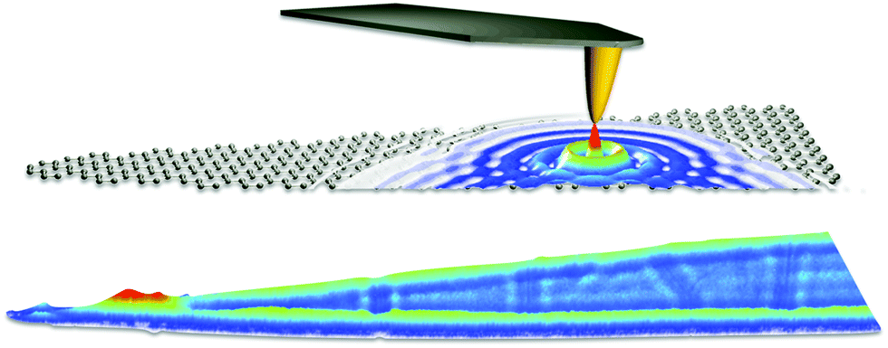 | ||
| Fig. 83 Top: Schematic of configuration used to launch and detect propagating surface waves. Bottom: Near-field amplitude image acquired for a tapered GNR on top of 6H-SiC. The imaging wavelength is 9.7 μm. The tapered ribbon is 12 μm long and up to 1 μm wide [adapted from ref. 1326]. | ||
From the theoretical point of view, plasmons in doped graphene have been studied by many authors.273,1593 These studies, however, employ random-phase-approximation (RPA),1594–1596 a theory successfully applied to normal Fermi liquids with parabolic bands in metals1597 and semiconductors.1597Ref. 1598 suggested that RPA misses some important physics in graphene, even in the long-wavelength limit. The plasmon dispersion in this material is indeed affected by potentially large many-body effects due to “broken Galilean invariance” (BGI),1598i.e. the existence of a cut-off in the dispersion. The pseudo-spin texture that characterizes the ground state of the Dirac–Weyl Hamiltonian provides an “aether” against which a global boost of the momenta becomes detectable. In a plasmon mode, the Fermi circle oscillates back and forth in momentum space under the action of the self-induced electrostatic field.1598 This oscillatory motion is inevitably coupled with an oscillatory motion of the pseudo-spins.1598 Since the exchange interactions depend on the relative orientation of pseudo-spins,1598 they contribute to plasmon kinetic energy and renormalize its frequency even at leading order in momentum.1598
It will be important to study the impact of BGI on the plasmon energy-momentum dispersion. This can be suppressed by e.g. inserting a sufficient number of BN layers between two SLGs. Since Coulomb interactions are long-ranged, one can achieve a regime in which inter-layer tunnelling is negligible, while e–e interactions are not. The intrinsic plasmon lifetime due to e–e interactions also needs to be calculated.
The study of plasmons and magneto-plasmons in graphene may be performed by means of electronic Raman experiments. This approach was extensively used for the investigations of plasmons and magneto-plasmons in ordinary semiconductor heterostructures,1599 but its application to graphene has been limited by the absence of favourable inter-band or intra-band resonant conditions matching the energy of available lasers. Indeed, light scattering can probe magneto-plasmons177,183,209,211,1600,1601 and coupled phonon-magneto-plasmons in SLG. The extension of these efforts to the study of plasmons and plasmon dispersions, in connection to the theoretical analysis discussed above, would provide new advances in fundamental understanding of graphene and will set the physical basis for the development of the THz detector technology.
Metamaterials and transformation optics,1602–1605 (i.e. media, possibly made of metamaterials, designed in such a way that they appear to perform a coordinate transformation from physical space to some virtual electromagnetic space1602) provide schemes for devices such as nanoscale waveguides, and superlenses.1606 Graphene metamaterials are promising, since electromagnetic field patterns can be tailored with nanoscale resolution and ultra-high speed through gate-tunable potential landscapes.
7.4. Graphene-based antennas
Throughout the last decades, communication has been enabled among different entities, ranging from mainframes to laptops and sensors. Along with the progressive shrinking in size of devices, engineers have developed efficient communication means tailored to the peculiarities of each type of device. The resulting networks have expanded the applications of the individual nodes by providing them a mechanism to cooperate. A good example of such applications is the Internet. The main challenge to enable communications among nanomachines, and at the nanoscale, is that reducing the size of a classical metallic antenna down to a few hundred nm would impose the use of extremely high resonant frequencies.1607Graphene-based nanoantennas (width: few nanometres, length: tens of micrometres) could be a key technology to overcome this issue, since this material supports the propagation of tightly confined SPPs.1608,1609 Due to their high effective mode index,1610 the SPP propagation speed can be up to two orders of magnitude below the EM wave propagation speed in vacuum. The main consequence is to reduce the resonant frequency of the antenna.1611 Recent works1612,1613 point to THz bands at short ranges, thereby enabling Graphene-enabled Wireless Communications (GWC).1158
The particularities of wireless communications at the nanoscale, their applications, and those aspects specifically inherent to GWC, such as the THz band, require that well-established communication protocols and network architectures undergo a profound revision in order to be applied to this scenario. One must develop a radically new medium access control (MAC), which provides channel access control mechanisms that make it possible for network nodes to communicate within a multiple access network, routing and addressing protocols along with network paradigms for GWC.
GWC might enable a variety of ICT applications. First, embedding nano-antennas into multi-core processors, allowing them to scale up to thousands of cores, and overcoming the challenge of global wiring and the associated delay. This multi-core architecture is known as Wireless Network-on-Chip (WNC).1614 Second, GWC may allow networks of small sensors that can measure nanoscale magnitudes with unprecedented accuracy. Nanosensors might measure physical characteristics of structures a few nm in size, chemical compounds in concentrations as low as one part per billion, or the presence of biological agents. Such networks of sensors, known as Wireless NanoSensor Network (WNSN),1615 are, per se, a new networking paradigm. WNSN require the integration of several nanoelectronic components and could be commercially feasible in 20 years from now. Third, GWC may enable communications in any device, regardless of its size. In this context, long-awaited applications such as true Ubiquitous Computing or Programmable Matter,1616 a material which inherently has the ability to perform information processing, may be possible with GWC. These applications may change the way in which society understands and interacts with technology, and push the boundaries of what technology can achieve.
Moreover, the flexibility of graphene coupled with the high σ74 and transparency,990 make it a good candidate for printed antennas on top of touch screens on smartphones. Traditionally, these types of antennas are based on ITO.1617 Furthermore, the variable resistivity can also lead to graphene's use in antenna design applications, as a smart material where its conductivity can be adapted according to external stimuli. Reconfigurable antennas may be designed controlling the radiation pattern and efficiency, depending on the application.1618E.g., stacking several layers of graphene the conductivity and bandgap could also be tuned. Therefore, graphene's properties could be tuned either by an external electric field, or through an interaction-induced symmetry breaking between several layers, thus leading to atomically-thin insulators or conductors.
7.5. Hybrid graphene-nanocrystal for light emitting devices
Shape controlled semiconductor core/shell colloidal inorganic nanocrystals (CINs) show advantageous luminescent properties,1619 including high quantum yield1620 and the possibility to precisely tailor their emission wavelength by tuning the core size.1620 The organization of such CINs into ordered arrays, e.g. micro scale ensembles of laterally and vertically aligned nanorods, has been achieved, with promising optoelectronic properties.1621Graphene can open up new horizons in terms of designing hybrid architectures consisting of light emitting semiconductor CINs1622,1623 and plasmonic MNPs.1624 Apart from being the scaffold for complex assembly structures, graphene can contribute to the functionality due to its electrical properties, which can be used for charge transport, but also for modulation of electrical interaction between metal and semiconductor NPs.
The aims are: (i) fabrication of homogenous and preferably ordered CIN layers on graphene, (ii) using graphene as a template for more complex NC assemblies, (iii) implementing graphene as a interface between metal NPs for plasmonics and semiconductor CINs for enhanced light emission, (iv) optimizing the graphene-NC interface for achieving efficient charge injection into semiconductor CINs while maintaining their bright emission, (iii) design of novel device architectures exploiting the flexibility of graphene.
The first aim is the controlled fabrication of NC layers on graphene surfaces in bilayer and multilayer configurations for light emitting applications, and the efficient charge injection from graphene into the CIN layer. In a 10 years perspective the target is the bottom-up approach to graphene-CIN based electrically-pumped LEDs and lasers, in which the optical gain material also constitutes the resonant cavity.
7.6. Graphene-based nanoscale optical routing and switching networks
The combination of graphene's electronic and photonic properties with its large-scale manufacturability and compatibility with Si technology make it a promising candidate for photonic integrated circuits.1483 These are based on the convergence and co-integration of a large number of passive optical components (such as waveguides, (de-)multiplexers, and filters) with active optoelectronic devices (modulators, switches and PDs) on a single chip. In most of the existing technologies, the typical length-scale of these active elements is large. Electro-absorption modulators and switches may be realized for optical, infrared and THz frequencies, at smaller length-scales. These devices, together with waveguide-integrated graphene PDs, might provide a toolbox of optoelectronic components for highly integrated optical interconnects.Specifically, graphene electro-optical modulators for visible and NIR frequencies could be integrated with Si waveguides. The energy spectrum and optical properties of graphene can be modified through an electrostatic field.1314 This was utilized to realize a broadband electro-absorption modulator,1314 based on optical absorption for photon energies 2EF < Eph and absorption suppression for 2EF > Eph due to Pauli blocking.1314 Due to the strong light–matter interaction (2000 dB cm−1 absorption1625), graphene-based modulators and switches may be realized on a smaller foot-print than devices using semiconductors, for electro-absorption or electro-refraction by the Pockels (i.e. birefringence in an optical medium induced by a constant or varying electric field1626), Kerr (i.e. change in the refractive index of a material in response to an applied electric field1627) and Franz–Keldysh (i.e. change in optical absorption in response to an electric field1628) effects. In order to achieve even higher integration densities and operation frequencies, ring resonators1629 and Fabry–Perot cavities with grating mirrors1630 are need. This might lead to higher modulation depth and speed than previously reported. The target should be operation at data rates >10 GBit s−1.
Alternatively, by combining graphene with plasmonics, it may be possible to enhance light–graphene interactions and achieve deeper modulation with smaller device size. Two alternatives, with optimized designs for modulation contrast and wavelength range, can be envisaged: (A) Fabrication and optimization of dielectric loaded plasmonic waveguides coupled with graphene aiming to achieve deep and high speed light modulation using low voltage graphene gating. These devices will operate from visible to NIR frequencies. (B) Exploitation of intrinsic graphene plasmons, for the wavelength range 2–10 μm, for which plasmons can be switched with virtually infinite on/off ratio.1326 By shaping graphene into 1d plasmonic waveguides, and with local electrostatic gating, the functionality of a nanoscale photon transistor may be realized. In addition, these plasmonic waveguides may be coupled to dielectric waveguides to interface with dielectric-based photonics to minimize losses.
The techniques and devices discussed above may be integrated in large-scale devices, to achieve M × 10 Gbit s−1 (with M the number of WDM channels) on-chip data transmission. The advantages of using graphene for photonic integrated circuits are manifold: simplicity, broadband operation, small footprint, and CMOS compatibility.
Graphene also offers a unique possibility to make electrically tuneable and ultrathin polarization modulators in the THz range and potentially up to MIR. Major applications, such as biosensing, pharmaceutical research, ultrafast wireless communications and environmental pollution control may benefit significantly from THz spectroscopy. Active control of the optical polarization is central for numerous applications in communication technology and optical physics, for material characterization and research methods. In the vast majority of applications the polarization is either fixed or controlled slowly by mechanical motion of the polarizing elements. Magneto-optical elements, such as Faraday rotators1631 (i.e. devices that rotates the polarization of light due to the Faraday effect) are typically thick because of the small Verdet constants, which give a quantitative measure of the Faraday rotation ability of the material.1631 This prevents using them in compact optical circuits, with a lack of broadband or spectrally tunable optical rotators.
The timeline is shown in Fig. 84 and the main targets for photonics and optoelectronics are: 3 years: Tunable metamaterials, plane-wave THz detection, electro-absorption and plasmon-based optical switches, graphene PDs for visible and IR, ultra broad-band tunable laser and long wavelength PDs. 3–7 years: Optical routing and switching networks, integration of ultra-fast and broadband model locked lasers, IR and THz camera and THz. Spectrometers, proof-of-concept system implementations. 7–10 years: Integrated graphene opto-electronic systems and circuits.
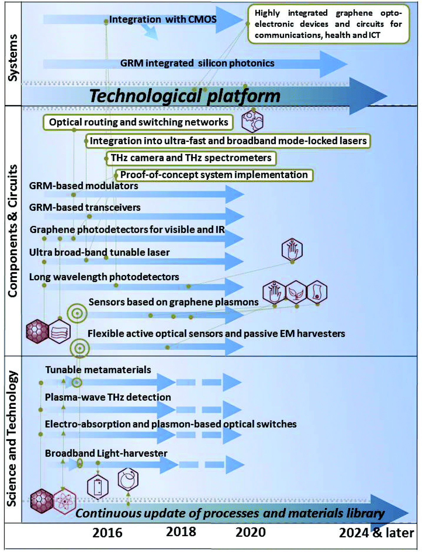 | ||
| Fig. 84 Photonics and optoelectronics timeline. | ||
8. Sensors
The rapidly increasing use of sensors throughout society, and the demand for cheaper and better devices with less power consumption, depend critically on the emergence of new sensor materials and concepts. GRMs have great potential for sensor development1326,1632 within a very wide range of applications, including industrial monitoring, surveillance, security, interactive electronics, communications, lab-on-chip, point-of-care, environmental monitoring, transportation and automation. This could result in a wave of cheap and compact sensor devices, with functionalities not seen in existing sensor technology.A sensor is a very general concept, covering essentially any device that converts physical quantities into a signal an observer can interpret. The target is to demonstrate proof-of-principle sensing schemes for a variety of applications: pressure sensors and microphones, mass (including gas) and force sensing, as well as electrical sensors for microwaves and biosensors. An essential part of the sensor is the read-out scheme. Mechanical, optical, electrical transduction schemes for GRM sensors must be explored.1632 Efficient transduction schemes that operate in a variety of environments (air, vacuum, liquid), as well as high pressures, high/low T and harsh conditions, are needed for applications.
In the short term, the development of GRM-based sensors will take advantage of the progress in high-frequency electronics, in particular concerning THz detection, as there is a lack of sensitive detectors for this frequency range. Optoelectronics is an interesting direction as it can provide new means for sensitive read-out and transduction schemes, and graphene-based plasmonic sensors1326,1633 for, e.g., chemical sensors with single molecule sensitivity. Furthermore, discoveries within the fundamental and spintronics research areas may lead to new detection schemes. The performance of sensor-based devices may profit from further development of better GRM fabrication methods, as well as from emerging flexible electronics technology, e.g. to realize cheap, scalable, flexible sensors.1634,1635 In a longer time-frame, when the working principle of novel GRMs sensor types will become established, the inputs and requirements e.g. derived from themes in section 3, might lead to the design and fabrication of highly specific, commercially competitive sensors.
In the coming 10 years, the challenge is to exploit the unique properties of GRMs,1636 optimise their chemical, optoelectronic and mechanical response for efficient on-chip individual and array sensors, and to integrate them with fast, accurate and cheap read-out.
GRM sensors can be divided in two categories: contact sensors, where substances make physical contact to the surface and induce a response, or non-contact sensors, that do not necessarily have to be in contact with the environment. Contact sensors include chemical and electrochemical sensors1637,1638 (gas and biosensors), as well as mass,1639,1640 mechanical force and stress1641 sensors, while optical/optoelectronic sensors,1642,1643 magnetic,1632,1644 radiation,1645,1646 electric field (single-electron devices),622 strain1634,1647 sensors are in most cases non-contact.
8.1. Contact sensors
In contrast to 3d materials, in GRMs each atom is in direct contact with the surroundings. The electronic properties of GRMs may be affected by small amounts of material, down to individual gas molecules.1648 So far, there has been a strong focus on supported graphene for sensor and electronic applications.1648 While suspended graphene is more difficult to produce and less mechanically stable, it is not influenced by substrate interactions, and can be a basis for nanoresonator devices due to the high rigidity, flexibility and strength1639 of graphene membranes. With recent progress in graphene synthesis and transfer, it will be of high priority to explore suspended graphene sensor concepts in theory and practice.The performance of a sensor critically depends on an efficient coupling between the quantity or process of interest and the sensing device. Supported SLG and various forms of graphene films602 offer the ultimate sensitivity to detect these tiny stimuli due to their large surface-to-volume ratio, while graphene membrane sensors can also benefit from their excellent mechanical properties i.e. high rigidity, flexibility and strength.1639
For most types of sensors, sensitivity is a key figure of merit. This is generally defined as the change of measured signal per stimulus (analyte or sensed physical quantity). Selectivity, the ability to discriminate one type or group of analyte/stimuli from others, is often just as important, e.g. for sensors that detect small concentrations of a specific substance. The response from chemical and electrochemical graphene sensors is generally non-specific, in that different analytes and stimuli may lead to similar response characteristics. To optimize and tune sensor performance, chemical functionalization or even deliberate introduction of defects can be necessary, i.e. to promote binding of specific analytes and, in this way, discriminate between the types of stimuli. Possible strategies to counter this challenge include sensor arrays with individually functionalised surfaces known from cantilever electronic noses1649 or discrimination based on the response characteristics of different substances in either time,1648 noise1650 or as a function of gate voltage. Selectivity is particularly important for applications within areas such as security,1651 environmental1652,1653 and point-of-care diagnosis.1654,1655 Other key features are response time, long-term stability, reliability and possibility to reset the sensor, for situations where the sensor itself cannot be replaced every time a response is recorded.
The strong tendency of graphene membranes to be contaminated with hydrocarbons is often attributed to the lipophilic (nonpolar),1656–1659 properties of graphite/graphene. Contamination may originate, e.g., from the transfer or lithographic processes, and removal of polymeric residues is a serious problem.602 Annealing in a controlled atmosphere, chemical treatment or current heating103,1030,1660 are widely used approaches. Cleaning using UV light is another promising process, which led to gas sensors capable of detecting down to sub-ppt (part per trillions) concentrations of a range of gases at RT.1661 To prevent further contamination in a realistic use-scenario, i.e. ambient, liquid or even hostile (high pressure, corrosive, radiation) environment, some of these options are impractical or even impossible. Real-time in-use cleaning or resetting is far more difficult than at the fabrication stage, as there is rarely a possibility of creating a controlled atmosphere, and physical accessibility and available power may be very limited. It may be necessary to treat graphene with a functionalisation1662 or protective/passivation1663 layer, which is non-trivial without compromising the integrity and sensitivity of the sensor. This could be particularly problematic for mechanical sensors. For some classes of sensor applications, one-time-use may be relevant, as, e.g., in airport security or point-of-care diagnosis, while continuous industrial or environmental monitoring typically require the sensor function to be recoverable, or at least possible to recalibrate. These challenges must be addressed, and approaches towards resetting, calibrating, protecting and maintaining sensor functionality need to be explored and implemented. Such considerations may also be relevant for non-contact sensors, although these are generally easier to protect.
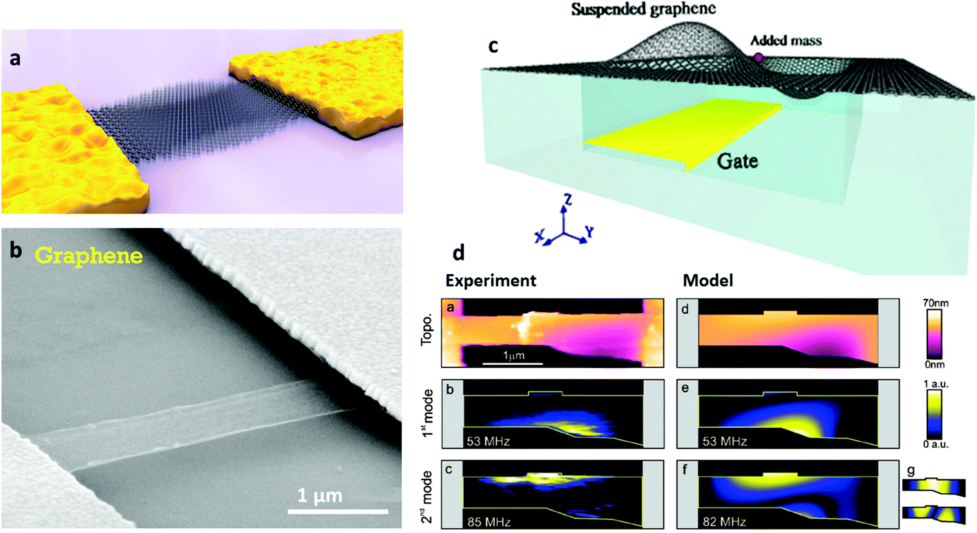 | ||
| Fig. 85 Graphene NEM structures. (a) illustration of a resonating beam of graphene connected to two electrodes. (b) graphene microribbon fabricated by etching the SiO2 support.1677 (c) Possible realisation of NEM spectrometer based on fully clamped graphene. By measuring the non-linear response from electrostatic actuation of the vibration modes, the mass and position of a particle can be determined.1678 (d) Measured and modelled topology of stressed graphene resonator. The eigenmodes of the graphene sheet measured using AFM are compared to finite element calculations.1679 | ||
The surface area-to-mass ratio of a graphene is very high (∼2630 m2 g−1),1667 hence even a molecular level of deposited material on a micro- or nanosize graphene membrane can constitute a measurable fraction of the total mass. Mass sensors based on graphene membranes were predicted to approach a mass resolution of 10−6 femtograms.1668 Although strong and flexible, graphene is nevertheless difficult to handle due to its extreme thinness.1659 Suspended graphene can be fabricated either by transferring CVD graphene onto a structure containing gaps, cavities or trenches,987,1669 by partial sacrificial etching in hydrofluoric acid of the SiO2 layer on which graphene is supported,144,145 or by mechanical exfoliation of graphene directly on trenches,1659 which is an un-scalable process.
For commercial purposes, graphene resonators are more promising than CNTs, since large-scale arrays with consistent dimensions are easier to produce1669 using top down microfabrication.1669 Graphene resonators may also benefit from a larger surface area, increasing the chance of interaction with the analytes. As each resonator will typically have a small capture area in order to obtain a high resonance frequency, large arrays of resonators can be a route to higher sensitivity and response rate, as well as higher spatial resolution.
One challenge for graphene membrane sensors is to achieve a sufficiently high Q-factor (quality factor) as broadening of the resonance peak will reduce the mass sensitivity accordingly. The Q-factor is the time-averaged energy stored in a resonator relative to the energy dissipated to the environment per cycle,1670 and is thus decreased by dissipative losses where the membrane is clamped, surface effects1671 and, in non-vacuum environments, also by viscous damping.1670,1671 While the Q-factor relative to thickness can be extremely high (∼1014 m−1 (ref. 1677)) for SLG membranes, the Q-factor itself is modest.1670 The highest reported values to date are ∼103 at RT1670 and ∼104–105 at cryogenic T.1670,1677 As the Q-factor of a membrane is inversely proportional to the surface-to-volume area Sv,1670 the product Sv·Q is a good indicator of the performance. A graphene resonator with Sv·Q = 14 000 nm−1 was reported,1670 compared to Sv·Q = 100 000 nm−1 for large SiN membranes.1670 Another figure-of-merit is the frequency-Q product. As sizes shrink, the frequency increases, while the Q-factor decreases.1650 Graphene resonators1672 reached frequency-Q products ∼1013, comparable to Si MEMS bulk resonators.1672
Strategies for improving the Q-factor include pre-stressing the graphene membranes, as well as clamping them on all sides to avoid dissipation caused by edge modes.1673 While studies of such nanodrums have so far shown resonance frequency in the MHz range,1640 the GHz range should be possible to reach1674 (see Fig. 86) by downscaling the resonators.
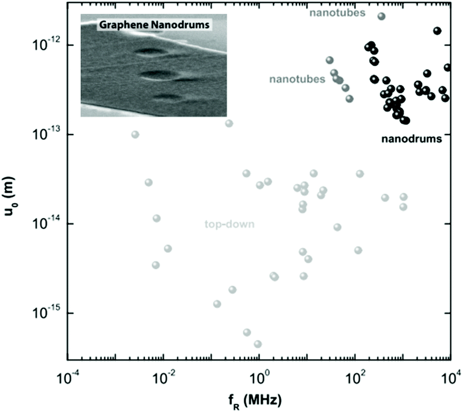 | ||
| Fig. 86 Resonance frequency and zero-point motion measured for a large number of top-down and bottom-up CNT and graphene nanodrum resonators. Graphene nanodrums are capable of reaching GHz resonance frequencies (adapted from ref. 1674). | ||
While tensile stress can directly improve the Q-factor, free-hanging graphene often suffers from slack after fabrication, e.g. caused by thermal expansion mismatch during T variations, e.g. after cleaning by thermal annealing. This can be counteracted by clamping to a polymer that shrinks drastically with T,1675 which was shown to increase the Q-factor to 7000 for a 10 μm beam.1675 In practical applications, particularly in liquid environments, ultrathin, large-area membrane resonators will be highly susceptible to viscous damping.1676 Reproducible and predictable wafer-level fabrication with large single crystalline grain sizes and a high cleanliness will be a necessary foundation for the development of effective graphene membrane sensors. Further research in device geometries to reduce losses, to control the tensile stress and to improve long-term stability is required as well.
Modelling is also crucial. Along with the Q-factor, the phase noise (random fluctuations in the phase)1650 is usually a limiting parameter for obtaining a high mass sensitivity.1666 The main goal is to understand the impact of thermal fluctuations, both mechanical and electronic, on the Q-factor of resonators and on the noise. In addition to detecting a frequency shift due to an adsorbed mass, it is also important to consider the effect of particles on the local mechanical properties. Another aspect to be studied is how the often strongly nonlinear resonant response of graphene resonators can be used for achieving higher sensitivity in mass-sensing,1680Fig. 85.
Although sensor applications often take place at RT or higher, the study of graphene resonators at low T allows a better understanding of the fundamental limits of graphene mechanics, and this will aid in improving performance of future. Mass sensing experiments can be pushed to extreme limits by monitoring the resonance frequency at low T.1688 Using this approach will eventually lead to improvement and better understanding of RT resonator sensing devices.
Sensitive electrical techniques to read out mechanical deformation and motion of graphene membranes at RT need to be developed. While thermal motion detection at RT was achieved using optical techniques,987 such techniques are not suitable for on-chip, CMOS compatible integration. It is thus necessary to explore various sensitive on-chip readout techniques, such as Si FET charge sensors and high-Q MW (microwave) resonant circuits. These devices may find application in microphones, pressure or gas detectors.
New electromechanical transduction schemes, in which parametric interactions will play a dominant role,1681 need to be developed. One of the possible parametric devices is a low-noise electromechanical microwave amplifier operating at low T, expected to reach the Heisenberg limit of lowest possible added noise.1672 In such a device, based on suspended graphene, the membrane would act both as a sensor as well the low-noise first stage preamplifier, enhancing the signal recovery efficiency. In general, these mechanical amplifiers would represent a simple and efficient alternative to nonlinear amplifiers such as Josephson amplifiers1682 and converters. Together with superconducting quantum interference device (SQUID) arrays,1683 these devices are essential for the implementation of highly efficient, quantum-limited homodyne detection (a method of detecting frequency-modulated radiation by non-linear mixing with radiation of a reference frequency1672) at MW frequency. By using mechanical mixing, suspended graphene devices may facilitate radiation detection even in the difficult THz band. A further opportunity offered by graphene-based electromechanical devices is that they can be easily driven into the nonlinear mechanical regime.1640,1684,2340
One application area for which NEM mass-sensing is immediately suited, is monitoring of aerosol content in the environment, which is important both for public health as well as for a better understanding of climate factors. This requires the NP's mass and size distribution to be accurately determined. While current commercial sensors can determine the distribution of particles with sizes down to the nm scale, there is a need for compact techniques, which can accurately and conveniently determine the distribution of particles in the 10–100 nm range. With an increasing need to monitor the environment in urban areas as well as the importance to ensure high safety standards in nanotechnology, such detectors are expected to have high commercialization potential. Since particle size is the primary concern, the material selectivity is less important, which will allow for a relatively fast development.
Graphene resonators also hold promise for biological and chemical analysis of very small amounts of liquid-phase solutions. A possible application is to analyse a blood solution by detecting the presence of different bio-molecules. The solution containing the bio-molecules may be electro-sprayed onto the sensor.1685 In order to detect as many bio-molecules as possible, the wafer may be covered by a large array of resonators with the surface of each resonator being as large as possible. Measurements using CNT resonators1686–1688 achieved sensitivity down to 1 yg (1 yg = 10−24 g), due to the low mass of the resonator. For graphene, sensitivities in the zeptogram (1 zg = 10−21 g) range have been estimated.1689
To fully exploit the potential for graphene mass-sensing, it is fundamentally important to establish proof-of principle integration of graphene resonator arrays,1669 with commercially available analysis front ends. Equally important is to tackle the problem of multiplexing large scale arrays and developing large scale fabrication methods to yield devices with high quality, as well as reproducibility. To this end, there is a need for further research ranging from graphene resonator readout and resonator fabrication to studies aimed at obtaining an understanding of how the interactions between graphene and NPs affects performance. Also, research on how to optimize graphene resonator properties, such as Q-factor and resonance frequency is important. If successful, the use of graphene resonators as detectors in spectrometric tools will provide a commercially sustainable means for NP detection, filling a missing gap in a critically important size range.
Ref. 1648 used a Hall bar graphene device, with the charge density in the graphene tuned to its lowest possible level to minimise electrical noise. This allowed detection of elementary charge adsorption events,1648 corresponding to individual gas molecules. Ref. 1648 estimated a detection limit in the ppb range, comparable to existing sensor technologies, and detection of gas molecules concentration in the sub ppt range has since been observed.1661 Graphene could become an important chemical sensor technology not just in terms of sensitivity, but also price. Compact devices may be fabricated in large areas, on rigid as well as flexible1696,1697 substrates, which greatly enhances the practical applicability compared to conventional solid state sensors.
Substantial efforts were done to relate the adsorption processes to the observed change in conductivity.1698 As the conductivity is proportional to both carrier concentration and μ, σ = neμ, it can be difficult to determine which, if not both, of these are affected by a specific adsorption process, i.e. whether the dominating process is a doping or a scattering effect. Ref. 1648 reported sign reversal of the conductivity change depending on the adsorbent being a donor or an acceptor (see Fig. 87), however, with minimal change in μ, as confirmed by others.1699 Numerous reports found μ improvement upon cleaning graphene from adsorbents.1700–1702 A better understanding of the adsorption processes and their effect on the electrical properties of graphene is necessary.
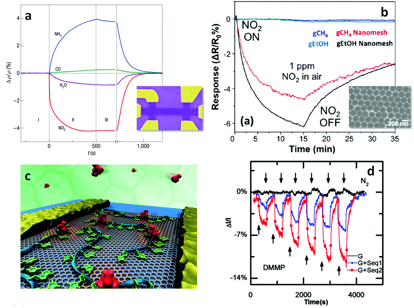 | ||
| Fig. 87 (a) Ref. 1648 demonstrated chemoresistive sensing using graphene field effect devices (inset), with the response depending on the type of analyte. (b) Nanopatterning can enhance the sensitivity of graphene chemical sensors. Ref. 1706 showed that large-area nanopatterning (inset) using colloidal lithography, could lead to a strongly increased response to various gas molecules. The gCH4 and gEtOH labels refer to graphene grown with methane and ethanol, respectively. The higher response of gEtOH samples was related to a higher defect density.1648 (c) Decoration with DNA molecules of a graphene field effect device can affect the chemoresistive response according to the specific DNA sequence. (d) Normalized changes in current vs. time for ssDNA graphene vapor responses. Lower arrows indicate introduction of analyte at progressively larger concentrations, while upper arrows indicate flushing with pure carrier gas. Graphene devices (black data) show very weak vapour responses that are barely above the noise floor. Devices functionalized with sequence 1 (red data with squares) or sequence 2 (blue data with circles) show significant responses that are sequence-dependent. Measurement of dimethylmethylphosphonate (DMMP) at concentrations of 20, 40, 60, 80, 100, and 120 ppm.1707 | ||
Contamination poses a serious challenge for graphene sensors, both in terms of cleaning during fabrication and for maintaining the integrity during operation. While most graphene applications directly benefit from a reduction of defects, contamination and corrugations, this is not necessarily the case for graphene chemical sensors. Similarly to CNTs, graphene has no dangling bonds on its surface. The gaseous molecules of interest may not easily adsorb onto pristine graphene surfaces.1703 The sensitivity may thus be limited by the chemical inertness, both by inhibiting chemical binding of analytes and functionalization layers.1704 A possible solution is the deliberate introduction of defects, which has been shown to enhance the chemical sensitivity of graphene conductivity sensors as compared to pristine graphene,1704,1705 as adsorbents predominantly bind to defects. Upon adsorption, edge and line defects have a far larger effect on conductivity than point defects, where current pathways around the defect exist.1705 While this situation may occur in other materials, graphene is superior due to its high σ (even when few carriers are present) and low noise, making even small changes in resistance detectable.1648
Functionalisation with molecules can improve the sensor performance in terms of sensitivity and selectivity. DNA deposited on a graphene chemical sensor improved response and recovery time, with the response being specific to a certain DNA sequence,1707 see Fig. 87(c and d). Large-area nanopatterning of graphene using colloid lithography was shown to be a viable route towards even higher sensitivities1706 (see Fig. 87b).
Functionalisation of free edges should make it possible to precisely engineer the molecular selectivity, ultimately to identify subtle changes in the chemical composition of species moving nearby those edges. Such sensors may benefit strongly from being integrated in a field effect device,1648 allowing to tune the carrier density to achieve maximum response per analyte, as well as a possibility of distinguishing molecules based on their field effect response or even their noise spectrum.1708 Thus, the essential challenge for graphene chemical sensors is to develop sensor concepts that allow for selectivity as well as sensitivity.
Mechanochemical functionalization (reaction with a liquid medium, such as alkynes and alkenes, to functionalize e.g., nanoparticle surfaces during their formation by mechanical process, e.g. by ball milling)1709 is a possible route towards higher tunability of graphene chemical sensors. The changes of chemical reactivity upon mechanical deformation of graphene or CNTs are well established,1710 and there are several routes to deliberate formation of curvature in graphene.1711Ref. 1712 reported that the reduced reaction barrier of strongly curved graphene promotes adsorption of hydrogen,33 and such covalent binding in turn leads to stable, atomically sharp kinks that can act as barriers for electron transport. Graphene sheets can be deposited on nanostructured substrates, and deformed according to the surface topology. Alternatively folds/kinks could be introduced via thermal mismatch.1713 Such deformations could lead to a modified chemical reactivity as a function of local curvature, and thus promote site-specific binding,1711 see Fig. 88.
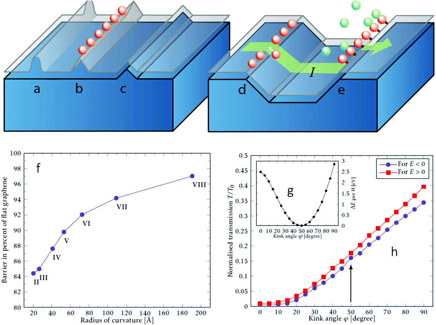 | ||
| Fig. 88 Proposal for mechanochemiresistive sensor. (a) folds increase chemical reactivity, allowing (b) localised binding of atoms or molecules, eventually leading to formation of atomically sharp kinks. (c) A fold pinned by a surface structure. (d) Atoms self-aligning on a kink. (e) Kink functionalisation to focus analytes, or to manipulate the sensitivity/selectivity of a chemoresistive sensor. (f) Reaction barrier at different positions of a curved graphene sheet.1712 (h) A line of hydrogen atoms in a place of high curvature could lead to a kink with an angle of 45–50°, and (i) electronic transmission through a single kink normalised by the transmission of pristine graphene (T0) as a function of the kink angle, φ, for electrons (E > 0) and holes (E < 0). The arrow indicates the normalised transmission at the equilibrium angle determined from the total energy calculations shown in h.1712 | ||
Enhanced sensitivity of chemical sensors as a direct consequence of pre-adsorbed contamination has been observed.1703 Such a mechano-chemiresistive sensor could rely on edge-adsorbed species to promote charge transfer from analytes, or even tune the affinity of certain analytes towards attaching to the graphene surface, see Fig. 88(a). Chemical sensor applications require clean, transferable SLG, FLG or RGO for consistent performances. Good electrical properties such as high μ, are not necessarily needed.
Other 2d crystals can also be explored, as alternatives or even complementary materials to graphene in hybrid devices.602 Hybrid hBN-graphene devices can be a route to tuning the physical properties of graphene devices in favourable directions,103,104,1714,1715 with several possible implications for sensing.
8.2. Non-contact sensors
Graphene-based MW detectors need to be investigated both theoretically and experimentally with the aim to improve the resolution of transistors for radar (W-band: 90 GHz) and telecommunication applications. The mid-term target is to push the working limits of transistors to the sub-THz domain (500–1000 GHz) where sensitive photon sensors are lacking both in terms of security and medical applications. The main issues are (i) the increase of μ for larger transit frequencies, (ii) the achievement of current saturation by optical phonons so as to increase the power gain, and (iii) the understanding of the role of acoustic phonons, which control hot-carrier T and limit sensor resolution.
Due to the excellent gate-channel coupling and low noise properties, graphene nanotransistors are a promising route to optimize the sensitivity-bandwidth product, thus paving the way to single-shot on-the-fly quantum coherent detection devices.
Nevertheless, the reason why graphene is suggested as a strain sensor1634,1723 is not the sensitivity, but the high mechanical flexibility combined with optical transparency, which paves the way for new applications in human-interface technology.1634 In comparison with most solid-state strain sensors, graphene-based sensors are better suited for polymer-based flexible electronics, displays and surfaces. Ref. 1634 demonstrated graphene-based strain sensors integrated into epoxy gloves, able to read out the bending of the fingers.
It was shown theoretically1724,1725 and experimentally1726,1727 that a large uniaxial strain can change the electronic properties in a way that closely resemble the effect of a large magnetic field. This pseudomagnetic field led to an experimental observation of QHE at zero field in highly strained graphene bubbles formed on Pt(111).1727 This effect could be envisioned for ultra-high level pressure sensors, with the pressure range being tuneable by adjusting the size of suspended graphene membranes.1726
Integrated Hall sensors have numerous applications, including automobiles, computers, industrial controls and consumer devices,1731 with a ∼870 BEuro market size,1732 and 90% of the market for magnetic sensors.1732 Graphene-based Hall sensors can be fabricated in a cross-shaped geometry,1731 in which the Hall effect is used to determine the magnetic field. Such sensors might be used to measure small magnetic particles, or be made into a scanning probe to map magnetic fields with a high spatial resolution.
Graphene, due to its low Hall coefficient RH = 0.3 × 10⁻⁶ Ωm T−1 [ref. 146] compared to RH = 4.3 × 10⁻⁶ Ωm T−1 for InAs,1632 is not an obvious candidate as Hall device material. However, performance comparable to existing Hall sensors was reported using CVD-graphene.1733 Magnetic sensors based on spintronics1632 and extraordinary magnetoresistance (EMR, i.e. very large magnetoresistance enhancement in composite metallic and semiconducting devices)127 may be routes to higher sensitivity. Ref. 1644, 1734 demonstrated a highly sensitive tuneable magnetic sensor based on a combination of the Hall and EMR effects. In terms of the tunable EMR magnetic sensor demonstrated by ref. 908, a high μ, as well as lower carrier density could provide a larger Hall resistivity relative to diagonal resistivity. Graphene in BN/SLG/BN multilayers908 can satisfy these two requirements, as well as offering devices of much smaller sizes than in conventional III–V semiconductor structures. The sensitivity of such a device can be further improved.1735 Having an active sensing layer thickness of atomic dimensions located at the device surface, combined with the ability to electrostatically tune the device's characteristics, paves the way towards magnetic field sensors capable of submicron spatial resolution, and tolerant to fabrication variations.
Further theoretical predictions of novel magnetic field sensors based on a graphene spin capacitors were reported,1736 suggesting the use of a GNR on top of an insulator connected to a ferromagnetic source/drain (with promising scalability and integration in current electronics). The large non-local spin current near the Dirac point shows that graphene may be used in spintronics without need of ferromagnetic materials to inject spin currents. This concept was demonstrated in a graphene-based spin capacitor.1736,1737 The time evolution of spin polarized electrons injected into the capacitor can then be exploited as a measure of external magnetic fields at RT. With a 100 ns spin relaxation time, magnetic fields ∼10 mOe may be detected,1736 the measurement accuracy depending on both density of magnetic defects and spin relaxation time.
Others explored the use of graphene SETs as a spin sensors for magnetic adsorbates,1738 to account for the experimental hysteresis in the linear magnetoconductance of gated graphene nanoconstrictions, operating in the Coulomb blockade regime. This behaviour was observed in two situations: when molecular magnets were deposited on graphene or CNTs,1739 and for bare graphene nanojunctions.225,715,1740
The possible bio-compatibility of supported graphene indicated by several cell proliferation studies1741,1742 and the enhanced sensitivity due to proximity of the graphene magnetic sensor to biological elements could be exploited in biotechnology research and applications.1743 Arrays of Hall nano-probes for the detections of magnetic NPs may work as magnetic markers in biomolecules. Hall nanoprobes may also be used as non-invasive heads in scanning magnetic probes. For low T applications, combination of graphene with superconductors may lead to quantum interference devices with extreme sensitivity to magnetic flux.1744 These may also be used to probe neural activity1745 in combination with other GFET biosensors.
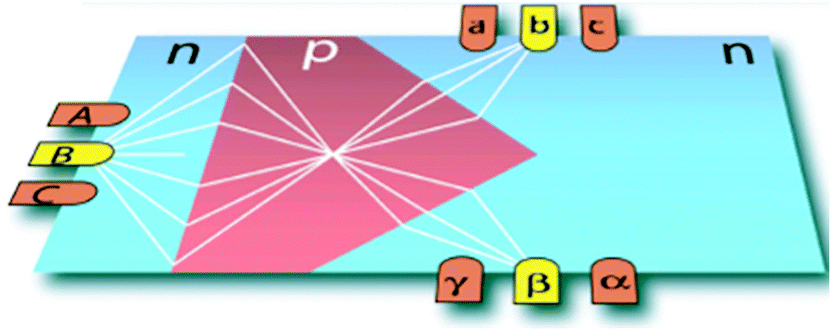 | ||
| Fig. 89 Prism-shaped focusing beam-splitter in a ballistic graphene n–p–n junction. Electrons emitted from contact B are distributed between contacts b and β. Adapted from ref. 143. | ||
8.3. 2d crystals and hybrids
Several other LMs are relevant for 2d sensor technology, both in enhancing the performance of the sensor layer and as sensing elements.Inorganic 2d crystals offer a range of properties relevant for sensors. Among these, MoS2 appears particularly suited due to its availability and electronic properties. Chemical sensors1746 have been fabricated from single and multi-layers MoS2, taking advantage of the semiconducting properties.
An example of a highly useful complementary material is h-BN, which is atomically flat and, unlike SiO2 and Si3N4, can be fabricated without charge traps and corrugations.1747 Graphene deposited on or stacked with h-BN is mechanically stabilized while experiencing little interference from substrate interactions, leading to very high μ.1747,1748
Highly sensitive MoS2 TFTs were fabricated with RGO as the contact layer, showing a detection limit for NO down to 2 ppb (ref. 1753), which was improved by a factor of 3 by Pt nanoparticle functionalization.1753
The sensor performance of 1L-MoS2 was found to be different from SLG,1746 with the response towards electron donors far higher than electron acceptors, due to the weak n-type characteristics of the investigated MoS2 devices. In particular, the response towards TEA (triethylamine), a laboratory-safe derivative of the V-series nerve gas agents,1746 was significantly stronger than in graphene, yet comparable to a CNT network, reportedly due to the TEA electron-donating properties.1746
The intriguing perspective of di-chalcogenides is the wide range of surface and electronic properties of the rapidly expanding library of processable layered compounds.1750 In combination with h-BN and graphene, the next-generation chemical sensors might be fabricated by stacking different LMs,1754 or by growth of lateral heterostructures.1755 This could increase the possibilities for engineering superior and application specific chemical sensor properties and, in particular, address the weak point of graphene-based chemical sensing, i.e. the lack of selectivity. An approach will be to perform simultaneous or multiplexed readout (i.e., the ability to read out many sensors simultaneously1756) in multiple sensor elements of different LMs followed by principal component analysis (i.e. a statistical approach to reduce the dimensionality of high-dimension data sets, while retaining most of the important variations1757). In the context of sensors, analytes that trigger different responses from multiple sensor elements are identified according to their response profile, rather than their multiple response to any individual sensor. Such an approach could lead to a higher selectivity and versatility of graphene chemical sensing devices. A key element in optimizing sensor performance will be to study the analyte–sensor interactions in detail and to identity the dominating response mechanism for the various LMs.
Sample fabrication and basic testing: Supported as well as suspended graphene membranes of different shapes and geometries of high quality and constancy must be fabricated. These will be single- and multi-layer depending on application.
Metal electrodes with properties to match diverse functions, such as source-drain contacts, top or bottom gate contacts or actuation/detection must be developed. Issues such as T stability, mechanical stability, contact resistance and doping/band-bending must be addressed, depending on application and use scenario. Basic mechanical and gate-dependent electrical properties of the devices need to be measured. The development of procedures for clean, low-damage transfer, cleaning and functionalisation/passivation must also be pursued. Strategies for enhancement or modification of chemical sensor sensitivity/selectivity also need to be developed, based on nanopatterning, defect engineering or molecular functionalisation.
Demonstration of sensor working principles: the detection methods need to be pushed to the limits, to achieve the highest possible sensitivity and selectivity without sacrificing robustness and predictability. For nanomechanical mass sensors in particular, methods for on-chip actuation and position detection should be developed. Modelling of the combined mechanical and electrical properties will play an important role. The aim is to develop single chips with integrated actuation, sensing and readout elements.
Technology and feasibility assessment supported by modelling: The suitability of the developed detection methods for use in industrial applications needs to be assessed. In addition, sensors will benefit from the developments in other fields to identify new applications (magnetic field sensors-based, or chemical FETs).
Important aspects to be considered are (i) size and cost reduction by using graphene as sensing elements, as it will increase the attractiveness of integrating multiple sensors with readout and actuation electronics in the same advanced CMOS chip and (ii) use of established or nearly established industrial process methods, such that the proof-of-concept devices may be industrialized as soon as industrial graphene-on-Si fabrication tools enter the market.
The timeline of GRM sensors is shown in Fig. 90 and the main targets are: 3 years: Single layer membranes. Gas sensors. Displacement detection with resonance amplitudes of 10 pm. Force sensitivity 520 zN/(Hz)0.5, microphone with a diameter of 600 μm with a sensitivity of 1 nm Pa−1. Single-molecule sequencing technologies such as those using protein pores. 3–7 years: Mass, chemical and pressure sensors. 7–10 years: Magnetic field sensors. On-chip scalable GRM sensors.
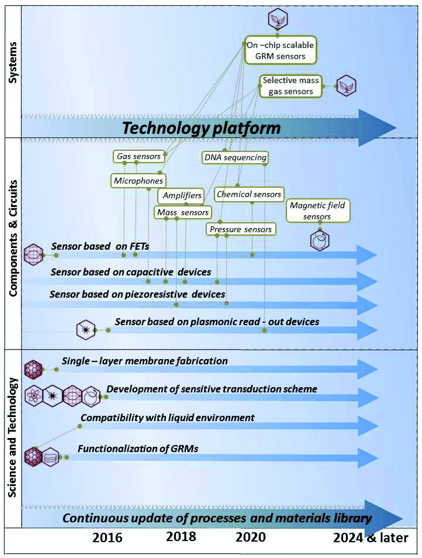 | ||
| Fig. 90 GRM-based sensors timeline. | ||
9. Flexible electronics
Flexible electronics is the next ubiquitous platform for the electronics industry.1758 The realization of electronics with performance equal to that of established technologies based on rigid platforms, but in lightweight, foldable, and flexible formats, would enable many new applications. This will bring truly conformal, reliable or even transparent electronic applications. It is also essential for rigid ultra-compact devices with tight assembly of components. It can also mean reduced cost and large electronic system integration by using novel mass manufacturing approaches, such as printed electronics, R2R or lamination, hitherto unavailable from more traditional brittle material and device platforms.Flexibility will not only permit new form factors, conformal systems and “wow effect” for consumer electronics, but will also improve reliability and create new kinds of electrical systems.1 Smaller, thinner and flexible electronic devices1758,1759 could be embedded to our world (or even into us) in a new fashion. E.g., enhanced flexible electronics solutions may deliver miniaturised, low cost and disposable sensors integrated in transparent and flexible surfaces. This would enable ubiquitous and energy autonomous sensors for the long awaited realisation of the internet-of-things1760 and everything-connected1761 sensor web, with application to smart homes, industrial processes, environmental monitoring, personal healthcare and more.
While a clear market pull exists and advantages of flexible and printed electronics are clear, the true revolution is still to come due to a number of technological challenges. First, commercial flexible electronics should be mechanically and electrically robust. Second, all used materials and components should meet essential performance criteria, such as low resistivity or transparency, even under mechanical deformation. Furthermore, materials should be environmentally acceptable. A full industrial and market adoption will also require that the platform allows integration of multiple technologies including active components. These requirements are impossible to combine with any existing high-throughput, low-cost mass-manufacturing solution. Graphene might lead to a flexible revolution, and graphene-based solutions might deliver benefits in terms of both cost advantage and uniqueness of attributes and performance.
As a thin flexible ultra-strong film1762 and an extremely good conductor, graphene is a natural choice also for flexible (and possibly transparent) electronic systems. It has several unique electrical, mechanical and optical properties, which might enable novel unforeseen applications as well as enhanced performance. Thanks to its intrinsic flexibility, graphene is ideal for sensors and devices that shall adhere and interact with the human body, enabling new consumer and medical applications not allowed by present technology.
Furthermore, other 2d crystals such as BN and TMDs, and heterostructures formed by their combinations can complement graphene technology. The development of such a new class of materials will further augment the impact on flexible electronics, by providing more functionalities and enabling new applications.
9.1. Key technology enablers
In order to enable the realisation of flexible electronics and optoelectronics, graphene technology should target the development of the core constituents of this new area: flexible electrodes (including all passive elements, such as interconnects and antennas), and flexible active devices (including RF transistors, sensors and LEDs). Also, transparency will be a key feature to achieve the fully deformable versions of various devices, such as light emitting diodes and touch panels. The combination of flexibility, electrical conductivity and transparency makes graphene technology potentially able to overcome the main issues related to various materials tested so far as TCs, such as ITO,1763 fluorine-doped Tin oxide (FTO)1764 and others, see section 9.2.1.Graphene-based electrodes, obtained either from inks or CVD films, may become available at a large scale, complying with various requirements in terms of σ and Tr, according to the different applications. E.g., for capacitive touch panels, Rs of a few hundreds Ω □−1 would be acceptable,10 whereas less than 50 Ω □−1 are needed for electrodes in solar cells10 and OLEDs.10 While transparency is also required for these applications, in other cases only a very low resistivity should be targeted. E.g., flexible antennas require flexible graphene films with resistivity less than 1–5 Ω □−1,1765 in order to achieve acceptable performance at ∼2–3 GHz.1765
The integration of graphene electrodes within active devices will require a proper engineering of the graphene work function, in order to achieve ohmic contacts and low contact resistance with other materials. In particular, graphene electrodes will be an advantageous choice in organic FETs, due to the low contact resistance achievable with organic materials.1766E.g., graphene provides low resistive contacts to pentacene where the current across these interfaces can be accurately modelled by a combination of thermionic and Poole–Frenkel emission.1767 In other cases, the graphene work function will need to be tuned, e.g. by doping or chemical functionalisation. In general, this will be a major advantage and opportunity with respect to ITO or other candidates for making flexible electrodes, whose work function can hardly be altered after the film deposition.1768
Graphene can act not only as a flexible electrode but, in some cases, also as an active component within a flexible device. E.g., graphene-based transducers can be implemented in flexible phototransistors or ChemFET (i.e. field-effect devices where the channel conductivity is tuned by adsorption of molecules1769,1770), exploiting both the material's sensitivity and form factor. High μ graphene channels may be used to enable flexible high frequency transistors. Also in this case, a key point will be the achievement of a suitable integration with the electrodes materials, in order to minimize the contact resistance.
In order to enable the practical realisation of graphene-based products, the full supply chain needs to be covered, from basic materials – such as inks and graphene substrates – to component development and finally to a full/complete flexible system integration and testing.
Therefore, the graphene-based flexible electronics activity should focus on the development of several key technology enablers, which also reflect the development of flexible electrodes and flexible active elements within key application areas:
Materials, fabrication and integration processes: Different fabrication approaches for graphene-based flexible electronics need to be studied, such as transfer and printing. The development of controlled and stable doping processes will be mandatory to achieve the required values of conductivity and contact resistance in all devices. Also, chemical functionalization processes will be needed in order to allow work function engineering and to control the interaction of graphene with flexible substrates such as Polyethylene terephthalate (PET), Polyethylene naphthalate (PEN), etc.
Integrating different graphene-based technologies: integration of flexible and rigid components, and 3d integration techniques all pose crucial challenges that have to be investigated deeply, with a special focus on scaling up the manufacturing of integrated components and hardware modules. The production of graphene in large wafer scale needs to be addressed, which would pave the way for high-speed circuits. Under most circumstances, graphene matches or exceeds μ and Tr of conventional materials, though Rs has proven somewhat less predictable and varies depending on production method, with CVD being the closest to optimal for solar and optoelectronics (highest Tr and lowest Rs) applications. On the other hand, printed electronics will be a major contributing factor in low cost high yield devices in daily applications. Hence, formulation of transparent conductive inks suitable for high-speed inkjet printing will be crucial for large scale manufacturing, together with the reliable production and transfer of homogeneous CVD graphene on a very large area.
Flexible energy solutions: Flexibility is also useful for energy-related technologies, such as energy storage and harvesting. Graphene-based electrodes could enable both large energy density and energy capacity in fully flexible energy storage devices, if low resistance and high surface area is achieved. Research topics include flexible batteries, super-capacitors and hybrid batteries-supercapacitors, as well as an expansion of their fabrication techniques to ink-jet printing, with its rapid, high volume R2R manufacturability. Graphene-based printable energy devices (see Fig. 91) are promising1771 and should be further developed.
 | ||
| Fig. 91 Graphene-based printed flexible battery.1771 Photograph of (a) as-produced graphene dispersion and (b) printed flexible battery. | ||
Flexible RF electronics and wireless connectivity solutions: Flexibility also creates new requirements for dedicated connectivity, such as RF interconnects and radio communication devices. Current flexible transistors have unity-current-gain frequencies, cut-off frequency – fT, and unity-power-gain frequencies, fmax, up to tens of GHz.867,867,1772,1773 Conformable antennas, flexible RF/EM shields as well as flexible high frequency electronic devices are envisaged. Graphene might also enable the evolution and deployment in flexible systems of radio technologies optimised for low power consumption and/or short range communication. Flexible and stretchable antennas using graphene may provide high speed tuneable operation including cognitive radio implementation, see e.g.ref. 1774.
Flexible graphene-based sensors: Graphene may also be used for large area biocompatible sensors and chemical sensors.1637 A flexible version of these may be one of the key technology enablers, as well as electromechanical and reliability tests of individual layers, substrates, devices and full systems. Topics that need to be investigated include graphene-based bio-chemical sensors, photodetectors and strain/deformation sensors. Developing chemical functionalization techniques for graphene sensing will be pivotal to achieve the desired capabilities. Other sensors that could be envisaged using graphene are strain, pressure and touch sensors, which would be conformable. Graphene-based sensors would need to perform reliably due to bending with radius of less than 100 mm in case of a wrist device.
Flexible passive electronics: Conductive transparent films are essential for flexible touch displays. Graphene is transparent, thin and highly conductive and it might replace present ITO-based TCFs, which are brittle and expensive.1775 Flexible touch panels are expected to be developed and integrated with the other graphene-based technologies, with a special focus on the environmental stability of graphene films, achievement of high patterning resolution, high μ and Tr.
In order to develop graphene-based flexible electronics systems within a coherent framework, a system level platform for flexible electronics needs to be built, for integration and testing of the various technology enablers at different stages of maturity.
9.2. Innovative flexible devices and user interfaces for consumer electronics
The field of transparent conductive coatings provides an exemplary application where graphene technology is likely to showcase its potential in terms of disruptive innovation in the consumer electronics industry, and not only. Wearable devices and new user interfaces (UIs) might be produced, providing strong innovation in the user experience, thanks to new features such as flexibility, stretchability and transparency.ITO suffers limitations: processing requirements, difficulties in patterning,1763,1778 sensitivity to acidic and basic environments. ITO is brittle and can wear out or crack in applications where bending is involved, such as touch screens and flexible displays.1779
Metal grids,1780 metallic NWs,1781 or other metal oxides1778 are other alternatives. Graphene combines high Tr with high conductivity, maintaining these properties even under extreme bending and stretching, ideal for integration in polymeric and flexible substrates. In many cases (e.g. touch screens or OLEDs), this increases fabrication flexibility, in addition to having economic advantages. E.g., present liquid-crystal-based devices face high fabrication costs associated with the requirement for large transparent electrodes. The move to a graphene-based technology could make them more viable. New forms of graphene-based TCEs on flexible substrates for solar cells could add value and a level of operational flexibility, not possible with current TCs and rigid glass substrates.
LMs such as h-BN, MoS2, WS2etc., have complementary physical and chemical properties to those of carbon-based nanomaterials and have the potential to fill a wide range of important applications either in isolation or as hybrids with graphene.
Graphene films have higher Tr over a wider wavelength range with respect to CNT films,1782–1784 thin metallic films,1780,1781 and ITO,1763,1777Fig. 92a. The flat absorption spectrum results in a neutral colour over a broad band.995 On the other hand, the minimum σ is ∼4 e2 h−1,74 resulting in Rs ∼ 6 kΩ for an ideal intrinsic SLG with Tr ∼ 97.7%. Thus, ideal intrinsic SLG would beat the best ITO only in terms of Tr but not Rs. However, real samples deposited on substrates, or in thin films, or embedded in polymers are never intrinsic. Exfoliated SLG has typically n ≥ 1012 cm−2 (see e.g.ref. 185), and much smaller Rs than the ideal case. The range of Tr and Rs that can be realistically achieved for graphene layers of varying thickness can be estimated taking n = 1012–1013 cm−2 and μ = 103–2 × 104 cm2 V s−1, as typical for CVD grown films.995Fig. 92b and c show that graphene can achieve the same Rs as ITO, ZnO–Ag–ZnO,1785 TiO2/Ag/TiO2 and CNTs with a much reduced thickness (Fig. 48b) and a similar or even higher Tr. Fig. 92c plots Tr versus Rs for ITO,1780 AgNWs,1780 CNTs1782 and the best graphene-based TCFs reported to date,1786 again showing that the latter is superior. E.g., taking n = 3.4 × 1012 cm−2 and μ = 2 × 104 cm2 V s−1, it is possible to get Tr = 90% and Rs = 20 Ω □−1, with better values for hybrid graphene–metal grids.1786
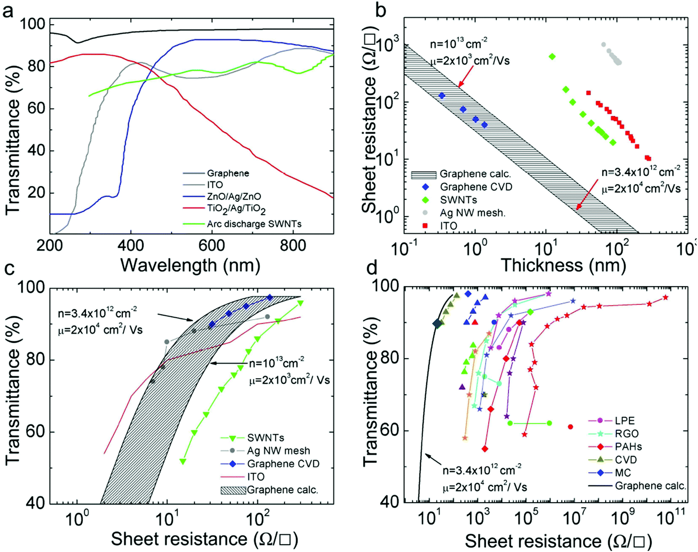 | ||
| Fig. 92 (a) Transmittance of graphene compared to different TCs: GTCFs,7 SWNTs,1782 ITO,1780 ZnO/Ag/ZnO (ref. 1785) and TiO2/Ag/TiO2 (ref. 1763). (b) Thickness dependence of Rs for graphene compared to some common materials; The blue rhombuses show roll-to-roll GTCFs based on CVD-graphene;7 red squares, ITO;1780 grey dots, metal nanowires;1780 green rhombuses, SWNTs.1782 Two limiting lines for GTCFs are also plotted using typical values for n and μ reported in the graph. (c) Tr vs. Rs for different TCs compared to graphene; blue rhombuses, roll-to-roll GTCFs based on CVD-graphene;7 red line, ITO;1780 grey dots, metal nanowires;1780 green triangles, SWNTs.1782 Shaded area enclosed by limiting lines for GTCFs calculated using n and μ as in b. (d) Tr vs. Rs for GTCFs grouped according to production strategies: LPE, RGO, organic synthesis using PAHs, CVD, and MC. triangles, CVD;7,9,824 the dark cyan rhombus is an hybrid metallic grid/graphene film;1786 blue rhombuses, micromechanical cleavage (MC);623 red rhombuses, organic synthesis from polyaromatic hydrocarbons (PAHs);710 dots, liquid-phase exfoliation (LPE) of pristine graphene;35,623,624,642 and stars, reduced graphene oxide (RGO).679,688,706,1788,1797 A theoretical line is also plotted for comparison. Adapted from ref. 995. | ||
Hybrid structures, such as graphene/metal grids1786 or solution processed graphene–CNT mixtures1793,1794 were also considered. Graphene/metal grids were prepared with Rs = 20 Ω □−1 and Tr = 90%,1786 and Rs = 3 Ω □−1 with Tr = 80%.1786Ref. 1793 achieved Rs = 100 Ω □−1 with Tr = 80% using solution processed graphene–CNTs. TC windows based on other LMs (e.g. Bi2Se3) have been fabricated on mica where the bonding to the substrate is through van der Waals forces1795 with Rs = 330 Ω □−1 and Tr = 70%.1795
A key strategy to improve the electrical performance is stable chemical doping. Ref. 622 prepared GTCFs, produced by MC, with Tr ∼ 98% and Rs = 400 Ω □−1, exploiting a PVA layer to induce n-type doping. Ref. 7 achieved Rs ∼ 30 Ω □−1; Tr ∼ 90% by nitric acid treatment of GTCFs derived from CVD grown flakes, one order of magnitude lower in terms of Rs than previous GTCFs from wet transfer of CVD films.7 Acid treatment permitted to decrease the Rs of hybrid nanotube–graphene films to 100 Ω □−1 for Tr = 80%.1796Fig. 92d overviews current GTCFs. It shows that GTCFs derived from CVD, combined with doping, could outperform ITO, metal wires and SWNTs. A hybrid graphene–metallic grid has shown promising results as a possible ITO alternative (Rs ∼ 20 Ω □−1; Tr ∼ 90%).
Note that GTCFs and GOTCFs produced by other methods, such as LPE, albeit presently with higher Rs at Tr = 90%, have already been tested in organic light emitters,691,1790 solar cells1788 and flexible smart window.995 These are a cheaper and easier scalable alternative to CVD films, and should be considered in applications where cost reduction is crucial.
Increasing the carrier density by doping is a means to reduce Rs. However, in most cases the stability of the dopant is unknown. Innovative doping routes need to be investigated, in order to achieve stable doping, preserving electrical properties over extended time scales. Doping simultaneous to growth can be achieved exploiting alternative precursors (e.g. pyridine, a molecule structurally related to the benzene ring but already with a donor nitrogen atom in the ring). Another route is “molecular doping” by stable hydrazil- and nitroxide- organic radicals.
Reliable transfer of large-area graphene onto arbitrary substrates is a critical step in the use of CVD-grown graphene. In many cases, the transfer process results in loss of material, and it is difficult to avoid contamination, wrinkling and breakage. Dry transfer techniques have also been developed,602 but need to be optimized for different substrates and conditions. The presence of the substrate generally modifies graphene's electronic properties and thus it is important to optimize interactions between graphene and substrate. One way is the modification of the substrate surface by applying surface treatments. The question is how the bonding of graphene to the various substrates affects the electronic properties. The variations with the support can, in turn, provide additional control of the graphene properties. A deeper understanding of these phenomena should be achieved, in order to use these effects for tailoring the chemical reactivity of supported graphene. For many aforementioned applications, thermal expansion and conductivity are crucial and will need to be investigated and optimised. Moreover, the combination of graphene and related 2d crystals should lead to significant charge redistribution at the interface. Thus, tuning of different parameters such as μ and work function should be studied.
Another approach is to develop processed LPE graphene deposited on a variety of flexible polymeric substrates to realize TCFs using an up-scalable, R2R coating, with the aim of achieving Tr ∼ 90–95%, with Rs < 100 Ω □−1 and tuneable work function. The achievement of these targets would permit the integration of GTCFs in many applications.
Characterization methods that are compatible with large areas will be required to monitor quality and consistency of as-produced GTCFs. Scanning probe microscopies as well as TEM are very suitable for investigation of selected regions with small to moderate areas, however, not practical for fast mapping of large areas. Apart from micro-Raman mapping and optical inspection, large-area mapping techniques will need to be developed, including conductivity probes and THz probes.
 | ||
| Fig. 93 Requirements for TC applications, SSL: Solid State Lighting; FPD: Flat Panel Display; ESD: ElectroStatic sensitive Device. Adapted from ref. 1806. | ||
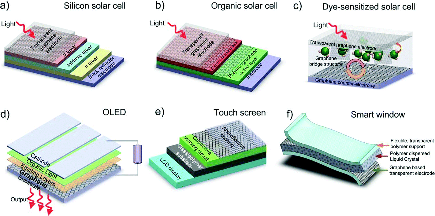 | ||
| Fig. 94 Graphene-based optoelectronics. (a) inorganic, (b) organic, (c) DSSCs, (d) organic LED, (e) capacitive touch screen, (f) smart windows.995 | ||
A uniform graphene layer can be transferred to the required substrate and large area graphene has been transferred to 30 × 30 cm2 substrates with low T lamination techniques.1799
Solar cells: The TC layer is a necessary component of all thin film solar cells and it has a major impact on efficiency, resulting in a 10–25% power loss even for the best TCs.1800 For the development or adoption of any new TC material, it is useful to know the impact on efficiency and the requirements to improve overall efficiency. Graphene can reduce losses, since it can have Tr > 90%, with Rs < 100 Ω □−1. A figure of merit is the ratio of DC conductivity and absorptivity (absorption coefficient). This does not depend on device architecture or film thickness and can be determined from Rs and absorption.
OLEDs: OLEDs can also take advantage of graphene.1790 They consist of an electroluminescent layer between two charge- injecting electrodes, at least one of which transparent.995 In these diodes, holes are injected into the highest occupied molecular orbital (HOMO) of the polymer from the anode, and electrons into the lowest unoccupied molecular orbital (LUMO) from the cathode. For efficient injection, the anode and cathode work functions should match the HOMO and LUMO of the light-emitting polymer.995 Traditionally, ITO is used as TCF. However, besides cost issues, ITO is brittle and limited as a flexible substrate. In addition, In tends to diffuse into the active OLED layers, which reduces device performance over time. Graphene has a work function of 4.5 eV,109,995 similar to ITO. This, combined with its promise as a flexible and cheap TC, makes it an ideal candidate for OLED anodes (Fig. 94d), while eliminating the issues related to In diffusion. Electroluminescence was also reported in graphene.1801 Although the power conversion efficiency is lower than CNTs,995 this could lead to light-emitting devices based on graphene.
Other 2d crystals have interesting optoelectronic properties. E.g., MoS2 layers are photoluminescent.378,1802,1803 We can thus foresee electroluminescent devices based on these materials. These will have advantages over traditional systems. They may be processable from solution, like organics, but they will not photo-oxidise like organics. This means they may be processable in ambient conditions.
Human Computer Interaction (HCI)1804 is a very important aspect of portable electronics, and new interaction technologies are being developed, including touch screens.1805 Touch panels are used in a wide range of applications, such as cell phones and cameras, and where keyboard and mouse do not allow a satisfactory, intuitive, quick, or accurate interaction with the display content.
Resistive and capacitive (see Fig. 94e) touch panels are the most common. Resistive touch screens comprise a conductive substrate, a liquid crystal display (LCD) front panel, and a TCF.1805 When pressed by a finger or pen, the front panel film comes into contact with the bottom TC and the coordinates of the contact point are calculated on the basis of their resistance values. The TC requirements for resistive screens are Rs ∼ 500 − 2000 Ω □−1 and Tr > 90% at 550 nm.1805 Favourable mechanical properties, including brittleness and wear resistance, high chemical durability, no toxicity, and low production costs are also important. GTCFs can satisfy the requirements for resistive touch screens in terms of T and Rs, when combined with large area uniformity. Ref. 7 reported a graphene-based touch panel by screen-printing a CVD sample. Considering the Rs and T required by analogue resistive screens, GTCF or GOTCF produced via LPE also offer a viable alternative, and further cost reduction.
On the other hand, capacitive touch panels are more versatile and work much faster than resistive panels and currently are used in many mainstream electronics applications.995 Capacitive touch screens are emerging as the high-end version of touch panels. These consist of an insulator such as glass, coated with ITO.1805 As the human body is also a conductor, touching the surface of the screen results in an electrostatic field distortion, measurable as a change in capacitance. The capacitive touch panel market is also driven by the chip vendors and manufacturers where the specification is critical to the Rs of the material. Moreover, effective drive and sense lines routing resistance, electromagnetic interference (EMI) shielding performance, low noise performance and transmission characteristics (Tr > 90%) are also crucial parameters.
A display is typically embedded in a touch panel, creating interference that must be shielded.1807 EMI shielding is usually achieved via a metal mesh structure,1808 which attenuates transmitting electric fields to a desired level. Importantly, an optimal shielding mesh should also be transparent, to avoid haze,1809 birefringence1809 and Moiré effects.1810 EMI shielding of RF radiation in electronic devices has become a serious concern,1807 and a very good average EMI shielding effectiveness, defined as1807 SE = −10log|Tr| (dB) where Tr is the transmittance of the shield, was reported for SLG on a flexible substrate.1807 In theory, SLG without defects or wrinkles can block as much as 97.8% of EMI.1807 Graphene composites could also be used for EMI. Therefore, graphene technology may provide new solutions for manufacturing transparent and flexible EMI shielding coatings, with impact in portable electronic devices and flexible electronics.
The challenges that graphene will be facing would be the Rs levels compared to ITO and Ag. The cost would offset ITO and Ag in comparison to graphene, but there needs to be some chemical modification of graphene in order to decrease Rs to below hundreds Ω □−1 from its intrinsic value while retaining Tr.
These touch panels solutions for HCI do not yet provide full satisfaction in terms of user experience,1811 as touch screens tend to be inert in the way they interact with a user. Also, the proliferation of icons, virtual keys and densely packed browsing menus on mobile touch screens requires increasing cognitive efforts from the user in order to locate, distinguish and manipulate them. Solutions for low-cognitive effort UIs,1812,1813 such as vibration enabled tactile feedback, are currently gaining momentum, and could improve usability, interaction interoperability, and user acceptance. Thus far, the most active tactile feedback solutions have been implemented through monolithic vibrations of the entire device driven by a single or very few vibrating actuators, typically electromechanical1814 or piezoelectric.1815 The types of tactile feedback that can be provided by such techniques are limited to quite basic patterns, only partially correlated to finger position, perceived audio-visual information and actions. Such solutions do not yet provide complete satisfaction in terms of user experience.
Key to this is the inability of monolithic vibrations to provide localized tactile feedback associated with visual images, and this is related to the difficulty in implementing tactile feedback directly from a display surface.1816,1817 To address the problem, a flexible and optically transparent graphene-based programmable electrostatic tactile (ET) system was developed capable of delivering localized tactile information to the user's skin, directly from the display's surface and in accordance with the displayed visual information (see Fig. 95).1758Ref. 1818 developed a transparent and stretchable graphene-based actuator, composed of transparent and compliant graphene electrodes and a dielectric elastomer substrate, for tactile displays. The graphene electrode is coated onto the designed region of the substrate layer by layer, thus only the area of the dielectric elastomer substrate with electrodes bumps up in response to the input voltage, which consequently produces actuation.1818 Apart from being simple in fabrication, cost-effective and extendible to multiple arrays, the actuator preserves its electrical and mechanical properties even under 25% stretching.1818
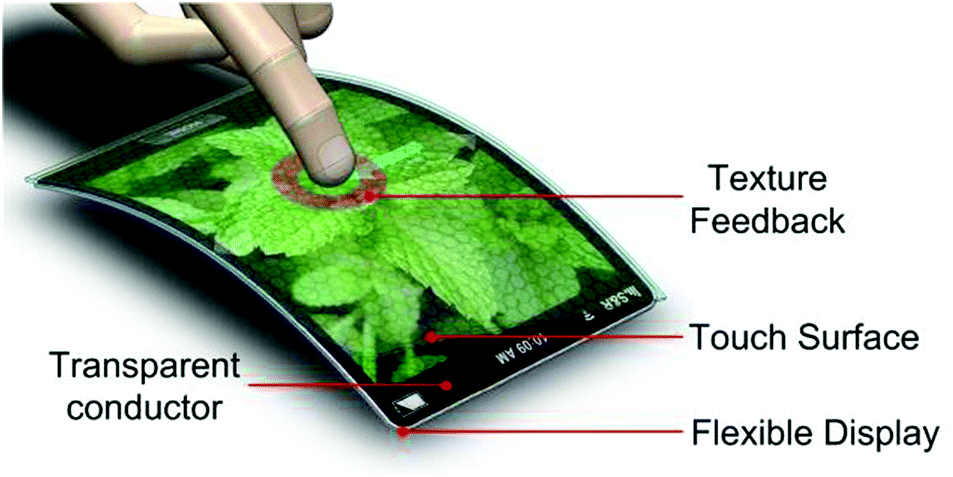 | ||
| Fig. 95 Graphene-based electrotactile display. Adapted from ref. 1758. | ||
Aside these “high end” applications, TCEs are used in several other every-day applications, such as low-emissivity windows in buildings,1758 electro-chromic mirrors1819 and windows,1819 static dissipation,1819 EM shielding,1819 invisible security circuits,1819 defrosting windows,1819 oven windows.1819 Considering the diversity of applications for TCs, different materials are most suitable for all uses. Depending on which material property is of most importance, different choices are possible.1819 However, considering that the majority of these applications do not require very low Rs (a Rs of a few hundreds of Ω □−1 can generally be used995) and that graphene can be produced in many different ways with diverse properties, GTCEs are likely to impact the TCEs market. In particular, GTCFs produced by LPE are appealing in low-tech applications, for ease of fabrication and low cost.
Electrically switchable optical shutters or similar structures, generally known as ‘smart windows’1820 are other devices that can take advantage from GTCEs. Smart windows consist of thin films of optically transparent polymers with micron-sized liquid crystal (LC) droplets contained within pores of the polymer.1821–1823 Light passing through the LC/polymer is strongly forward scattered, producing a milky film. If the LC ordinary refractive index is close to that of the host polymer, the application of an electric field results in a transparent state.1824 The ability of switching from translucent to opaque makes them attractive in many applications, e.g. where privacy at certain times is highly desirable. There are other potential applications of PDLCs in flexible displays, such as an organic thin film transistor driven flexible display with each individual pixel controlled by an addressable PDLC matrix.1824 Conventionally, ITO on glass is used as TCF to apply the electric field across the PDLC. One of the reasons behind the limited market penetration of smart windows is the significant ITO cost. Furthermore, flexibility is hindered when using ITO, reducing potential applications, such as PDLC flexible displays.1824 For transparent or coloured/tinted smart windows, the required Tr and Rs range from 60 to 90% and above and 100 to 1 kΩ □−1, depending on production cost, application and manufacturer. In addition to flexibility, the electrodes need to be as large as the window itself and must have long-term physical and chemical stability, as well as being compatible with R2R PDLC production process. LCs could also be used for next-generation zero-power monochromatic and coloured flexible bi-stable displays, which can retain an image with no power consumption.1825 These are attractive for signs and advertisements or for e-readers, and require TCs for switching the image. The present ITO devices are not ideal for this application, owing to the limitations discussed above.
1519 is suitable for applications in electronics on soft substrates. Since pristine graphene has no bandgap,74 the availability of other 2d crystals is essential for the development of novel flexible electronic devices. Flexible MoS2 FET devices have been reported with ION/IOFF > 107 and μ ∼ 30 cm2 V s−1 using high- dielectric, such as hafnium oxide.1828 Replacing the conventional dielectric (e.g. Aluminium oxide) with BN on MoS2 transistors may enable flexible and stretchable high-speed electronics and RF devices. The combination of the properties of various 2d crystals in heterostructures will open new opportunities in many fields of flexible electronics.
Applications that might be enhanced by the development of 2d crystals can be identified in the field of flexible electronics:
1. Flexible TFT and RF devices . The use of 2d crystals in hybrid 2d devices on flexible substrates (e.g. using BN as a dielectric and MoS2 or WS2 as a semiconductor) may solve the problem of the lack of a bandgap in pristine graphene for flexible TFTs. The combined use of atomically flat 2d dielectrics, such as BN, may enable high μ flexible transistors for high speed flexible electronics. Also, strain engineering of the bandgap of 2d crystals1829 may offer new solutions for flexible electronic devices.
2. Flexible optoelectronics . Due to its direct bandgap, 1L-MoS2 is a promising material for optoelectronics. A tunability of the bandgap is predicted in heterostructures made by stacking different 2d semiconducting crystals (e.g. MoS2 and WS2) in different ways,1830 opening the opportunity to engineer new optoelectronic materials. Therefore, novel flexible optoelectronic devices will be enabled by the development of the 2d crystals technology. Heterostructures based on 2d crystals have also a great potential for flexible photovoltaics. Light–matter interaction can be strongly enhanced in 2d crystals heterostructures, leading to an EQE ∼30%.1529
3. Flexible sensors . In the field of chemical sensors and biosensors, the combination of various 2d crystals and graphene derivatives may offer the opportunity to add selectivity to the high sensitivity typical of these all-surface materials. Arrays of sensors made of different 2d sensing materials may be integrated on top of flexible substrates, and a specific response to the analytes may be achieved via neural network approaches (e.g. “electronic nose”1831). Furthermore, flexible strain sensors may be developed based on the sensitivity of 2d crystals to deformation.
The main development steps toward flexible electronic devices based on 2d crystals are:
– Materials. Suitable inks for screen and inkjet printing on flexible substrates have to be developed. A library of functional inks based on 2d crystals will enable flexible printed devices, such as sensors and transistors. Large area deposition or growth processes (such as CVD) need to be developed for 2d crystals, together with suitable (clean) post-processing methods (transfer on flexible substrates, annealing). Controlled doping techniques have to be identified.
– Integration. Compatible processes for manufacturing integrated hybrid graphene/2d crystals-based devices must be developed, together with suitable flexible substrates for the integration of hybrid structures. A good control of the interfaces should be achieved in manufacturing 2d heterostructures, controlling both the coupling between different 2d crystals and the interaction with the substrate.
– Mechanical performance. In general, 2d crystals are flexible, but the combined use of conventional materials and electrodes in flexible devices can create constraints in terms of flexibility and repetitive bending, due to the brittle nature of metals and dielectrics such as HfO2 and Al2O3. Suitable combinations of graphene, BN and semiconducting 2d crystals should be identified for ultrathin, transparent and flexible devices. The flexibility of electronic devices made of different 2d crystals and of hybrid 2d crystals structures must be assessed by mechanical tests (bending cycles) on different flexible substrates. The effect of defects on the mechanical properties needs to be studied and controlled. The flexibility of printed films has to be studied, and the 2d crystals inks need to be tailored accordingly in order to achieve good performance upon mechanical cycling.
9.3. Outlook
In order to have the foreseen impact, all essential technology parts need to be linked together. In a 10-years perspective, the vision for flexible electronics and optoelectronics can be built upon the previously mentioned key technology enablers, which can be then unified around two streams of applications, as summarized in Fig. 96. | ||
| Fig. 96 Two identified streams of GRM applications targeted for flexible electronics and optoelectronics. | ||
The short term target should be related to the development and the increase in maturity of the previously listed key technology enablers, which may be then deployed for the realisation of ambitious goals in the mid/long term. During the development of the two application streams shown in Fig. 96, the demonstration of novel flexible devices is expected.
In the first application stream (“Smart Portable Devices”) the realisation of the following major prototype demonstrators can be envisaged:
Wearable smart devices for sensing and connectivity. Leveraging both existing and new graphene and 2d crystals-based technologies these demonstrators will show the potential for cost advantage and/or performance enhancement in wearable, connected devices for the emerging market fitness and wellness application.
Bendable and portable smart devices for entertainment and browsing applications. Combining advanced material, energy, connectivity and integration/manufacturing technologies with display and logic processors from external suppliers, this will showcase radically new solutions for game control and user interaction and manipulation of content.
Partly or fully flexible mobile phones. The most advanced and challenging demonstrator that can be envisaged at this stage will attempt to reproduce important functionalities of a smart phone in a partly or fully flexible format.
In the second application stream (“Energy Autonomous Sensors”) the realisation of the following major prototype demonstrators can be envisaged:
Graphene-based chemical and bio-sensors. Exploiting both existing and new sensing devices with high or ultra-high sensitivity and chemical stability, based on graphene functionalization chemistry, intrinsic biocompatibility and ambipolar characteristics of graphene–FET devices, and distinct sensitivities of different 2d crystals.
Energy harvesting and storage devices. Developing energy related technologies tailored for flexible substrates such as flexible batteries, super-capacitors and their integration with harvesting devices would provide the “engine” to propel the autonomous sensor devices.
Integrated smart sensor units with RF connectivity. At first, RF device and circuit applications based on ambipolar non-linear graphene electronics for RF connectivity might be combined with analogue sensor interfaces, and integrated on a flexible substrate. Finally, the necessary infrastructure towards “graphene-augmented” smart integrated sensors on flexible substrates should be developed, together with the necessary energy harvesting and storage capability to work autonomously and wirelessly connected to the environment.
The combination of the developed materials, manufacturing techniques, components and circuits is expected to enable the creation of a new technological platform based on 2d crystals, where real flexible electronic systems could be built.
The timeline for the GRM flexible electronics and optoelectronics is in Fig. 97. The main targets are: 3 years: GRM inks for flexible electronics; reliable processing of CVD graphene on flexible substrates; flexible touch panels; flexible antennas. 3–7 years: Flexible UI; flexible wireless connectivity; flexible sensors; flexible energy storage and harvesting solutions; heterogeneous integration 7–10 years: flexible intelligent devices.
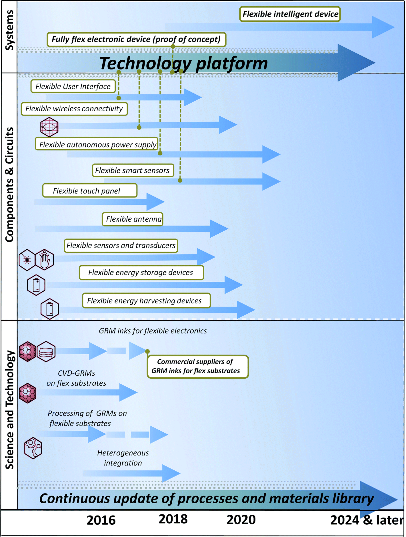 | ||
| Fig. 97 Flexible electronics timeline. | ||
10. Energy storage and conversion
Storage and conversion are essential for energy production and saving. Energy can be stored in a variety of ways depending upon the intended use, with each method having its advantages and disadvantages. Batteries, capacitors, and fuel cells have been used and studied for over a century to store energy. The need to develop sustainable and renewable energy sources is leading society to develop energy from sources that are not continuously available, such as Sun and wind. In addition, there is a significant need to have portable energy not only for portable devices, but also for transportation, to decrease the reliance on fossil fuels. Batteries and electrochemical capacitor storage devices are the most common means of storing energy, and fuel cells are also coming into their own. However, there are a number of challenges that need to be addressed to improve their performance and their viability. Therefore, high energy electrodes are increasingly important. The Ragone plot,1833Fig. 98, a graph, named after D. A. Ragone, of power against energy density of energy storage devices, permits to compare different technologies and judge their usefulness for a particular application, e.g. when high energy density or power density is needed.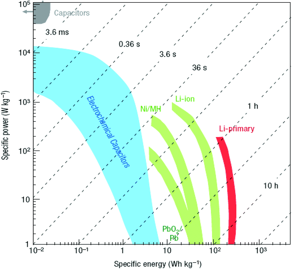 | ||
| Fig. 98 Specific power as a function of specific energy [energy per unit of weight], also called Ragone plot,1833 for various electrical energy storage devices. Characteristic times correspond to lines with unity slope. The characteristic time of an application is of the order of the energy-to-power ratio of the energy storage device and in the log–log plane of the figure, the time corresponds to straight lines. Capacitors are useful for short time applications <0.01 s, while batteries are useful for long time applications >100 s. See ref. 1832 for a detailed discussion of the Ragone plot. Li Primary are not rechargeable batteries. Secondary ones are rechargeable. Ni/MH indicates Ni metal hydride batteries. | ||
10.1. Batteries
Many forms of storage exist, including large-scale storage such as hydroelectric power and compressed air, as well as fly wheels and electrochemical energy storage (Li-ion batteries, redox flow batteries and supercapacitors).At present, Li-ion batteries, using the chemistry of a LiCoO2 cathode and a graphite anode,1834–1837 are considered by the batteries community the leading candidates for hybrid, plug-in hybrid, and all electrical vehicles, and for utility applications. The energy density and performance of Li-ion batteries largely depend on the physical and chemical properties of the cathode and anode materials. Conventional Li-ion batteries utilize graphite as the anode.1838 The low theoretical specific capacity (i.e. the total ampere-hours (Ah) available when a battery is discharged at a defined value of discharge current, per unit weight) of graphite (372 mA h g−1 [ref. 1838]) makes it important to find alternative negative electrodes. Si (4200 mA h g−1)1839 or Sn (994 mA h g−1)1840 have higher capacity. However, their application as anodes in Li-ion batteries has been limited by their poor cycling (i.e. the number of charge/discharge cycles before the battery fails to meet performance criteria, e.g. specific capacity below 60% of nominal value) caused by large volume changes during the uptake and release of Li.1841 The search for suitable cathode and anode materials has proven challenging. The possibilities for the improvement of cathode materials are quite limited due to the stringent requirements, such as high voltage potential, structural stability, and inclusion of Li in the structure.1842,1843
Many potential electrode materials (e.g. metal oxide) in Li-ion batteries are limited by slow Li-ion diffusion1836,1837 and poor electron transport1836,1837 at high charge/discharge rates.1836,1837 To improve the charge-discharge rate performance of Li-ion batteries, extensive work focused on Li-ion and/or electron transport in electrodes.1844 Nanostructures (e.g., nanoscale size1845 or nanoporous1846 materials) have been widely investigated to improve Li-ion transport in electrodes by shortening the Li-ion insertion/extraction pathway.1844,1847
A variety of approaches were developed to increase electron transport in the electrode materials, such as the use of conductive coatings (e.g. carbon black, CNTs1848–1850). In Li+ batteries, higher energy requires electrodes with high conductivity and improved resistance to reaction with electrolytes. Graphene may be an ideal conductive additive for hybrid nanostructured electrodes.1851,1852 Other advantages include high surface area (theoretical ∼2630 m2 g−1)1667 for improved interfacial contact and potential for low manufacturing cost.
High-surface-area RGO sheets were studied for Li-ion storage.1853 In addition, RGO was used to form composites with SnO2 in order to improve specific capacity and cyclic stability of anodes.1854 GRMs were also used as a conductive additive in self-assembled hybrid nanostructures to enhance the performance (i.e., charge/discharge capacity, and current and energy density) of electrochemical active materials.1855,1856 However, the majority of electrodes were fabricated exploiting CMG and only recently the full potential of graphene produced by LPE was exploited622 in electrodes for Li-ion batteries. Ref. 622 reported that electrodes based on Cu-supported graphene nanoflakes ink can reach specific capacities ∼1500 mA h g−1 at a current rate ∼100 mA g−1 and specific capacities ∼650 mA h g−1 at a current rate ∼700 mA g−1 over 150 cycles, when tested in half-cell configuration (i.e. with a structure that contains a conductive electrode and a surrounding conductive electrolyte separated by a Helmholtz double layer). By balancing the cell composition and suppressing the initial irreversible specific capacity of the anode (∼7500 mA h g−1), principally due to the decomposition of the electrolyte at the surface of the electrode with the formation of a solid electrolyte interphase (SEI), ref. 622 reported an optimal battery performance in terms of specific capacity, i.e. 165 mA h g−1, estimated energy density ∼190 W h kg−1, operation over 80 charge-discharge cycles.
Table 6 summarizes the performances (i.e., charge/discharge capacity, and current and energy density) of GRM-based Li-ion batteries reported to date.
| Material | Discharge/charge capacity | Current density | Ref. |
|---|---|---|---|
| a Li-air battery. | |||
| Cathodes | |||
| Commercial LiCoO2 | Specific capacity 140 mA h g−1 | N/A | |
| Sulfur/GO | Specific capacity 950 mA h g−1 | Current density 168 mA g−1 | 1867 |
| Sulfur/RGO | Specific capacity 600 mA h g−1 | Current density 334 mA g−1 | 1868 |
| Li3VO4/RGO | Specific capacity 223 mA h g−1 | Current density 8000 mA g−1 | 1869 |
| LiMn0.75Fe0.25PO4/GO | Specific capacity 107 mA h g−1 | Current density 8500 mA g−1 | 1870 |
| Anodes | |||
| Commercial graphite | Specific capacity 372 mA h g−1 | N/A | |
| RGO electrodea | Specific capacity 15000 mA h g−1 |
N/A | 1871 |
| RGO electrode | Discharge and charge capacities of 2179 and 955 mA h g−1 for graphene, 1105 and 817 mA h g−1 for Co3O4 and 1097 and 753 for Co3O4/graphene composite | N/A | 1872 |
| RGO electrode | Specific capacity 1200 mA h g−1 | Current density 100 mA g−1 | 1873 |
| CVD Graphene | Discharge capacities of 0.05 (500 mA h g−1) and 0.03 mA h cm−2 (500 mA h g−1) for pristine and N-doped graphene respectively. | Current density 5 μA cm−2 (50 mA g−1) | 1874 |
| (1) RGO electrode | RGO: Specific capacity ∼820 mA h g−1. | N/A | 1875 |
| (2) Graphene-PANI composite | Irreversible capacity loss (685 mA h g−1) | ||
| Graphene-PANI composite: Specific capacity ∼800 mA h g−1. | |||
| Irreversible capacity loss (545 mA h g−1). | |||
| Reduced GO (via pyrolytic and E-beam) electrode | GO: 758 and 335 mA h g−1 discharge and charge capacity | Current density 50 mA g−1 | 1876 |
| Pyrolytic reduction: 1544 and 1013 mA h g−1 | |||
| E-beam reduced GO: 2042 and 1054 mA h g−1, respectively | |||
| CMG electrode | Discharge capacity ∼528 mA h g−1. | Current density 50 mA g−1 | 1877 |
| Discharge capacity ∼298 mA h g−1 for CMG electrode. | |||
| RGO electrode | Specific capacity ∼945 mA h g−1 in the initial discharge. Reversible capacity ∼650 mA h g−1. | N/A | 1878 |
| Specific capacity ∼460 mA h g−1 after 100 cycles. | |||
| RGO | Specific capacity 370 mA h g−1 | Current density 1860 mA g−1 | 1879 |
| LPE Graphene | Specific capacity 650 mA h g−1 after 150 cycles. | Current density 700 mA g−1 | 622 |
| GO/TiO2/Super p hybrid electrode | Specific capacity of the hybrid material of 87 mA h g−1 (35 mA h g−1 for rutile TiO2 only); specific capacity of anatase TiO2/graphene of 96 mA h g−1 (compared with 25 mA h g−1 of anatase TiO2). Graphene only initial capacity of 100 mA h g−1 | N/A | 1855 |
| MoS2/GO, Mo:C molar ratio 1:2 |
Specific capacity 1100 mA h g−1 | Current density 1000 mA g−1 | 1880 |
| MoS2 | Specific capacity 700 mA h g−1 | Current density 1000 mA g−1 | 1860 |
| ZrS2 | Specific capacity 470 mA h g−1 | Current density 552 mA g−1 | 1862 |
| SnO2/RGO | Specific capacity 810 mA h g−1 | Current density 50 mA g−1 | 1881 |
| Co3O4/RGO | Specific capacity 800 mA h g−1 | Current density 50 mA g−1 | 1872 |
| Mn3O4/RGO | Specific capacity 350 mA h g−1 | Current density 1600 mA g−1 | 1882 |
| Fe3O4/RGO | Specific capacity 500 mA h g−1 | Current density 1750 mA g−1 | 1883 |
| Si–GO | Specific capacity 1100 mA h g−1 | Current density 8000 mA g−1 | 1884 |
| Ti3C2 | Specific capacity 110 mA h g−1 | Current density 110 mA g−1 | 1865 |
Graphene as hybrid system with VO5 could be used as cathode to fabricate flexible, thin film Li-ion rechargeable batteries. Here, graphene could act as the flexible current collector, replacing the traditionally used Al, offering additional volumetric capacity, electrochemical stability and mechanical flexibility. In addition, free-standing or substrate-bound, electrochemically lithiated graphene, can be used as anode.
For batteries, future activities should focus on graphene-coated lamellar Li+ hosting oxide electrodes, graphene nanocomposites with Li+ intercalated between graphene sheets for improved morphology preservation at the nanoscale during battery charge/discharge, and graphene–Si composite electrodes with additives for more stable surface electrode interphase. The long term aim would be to develop novel Li–O2 battery concepts (Li–O2 is a metal–air battery that uses the oxidation of lithium at the anode and reduction of oxygen at the cathode to induce a current flow1857), able to supply high energy density (∼3500 Wh kg−1 [due to the high specific energy density of lithium with respect to air (3840 mA h g−1)1857,1858], an order of magnitude more than a conventional Li battery).1858
Graphene may also be used in other energy storage systems as current collector. In this case, free-standing or substrate-bound films with high accessible surface area to volume ratio could replace traditional activated carbon materials (i.e., processed to have small, low-volume pores that increase the surface area available for adsorption or chemical reactions) in the cathode and as current collectors in transparent devices.
TMDs, TMOs, trichalcogenides and TMHs (transition metal hydroxides) are promising alternative materials for Li-ion batteries.1859,1880 The weak VdWs interaction between the layers may allow ions to diffuse without a significant increase in volume expansion. Some of the TMDs are accessible for Li ions intercalation and exhibit fast ion conductivity [i.e. the movement of an ion from one site to another through defects in a solid], such as exfoliated MoS21860 and TiS2.1861Ref. 1860 reported a 800 mA h g−1 reversible specific capacity when using MoS2 as battery electrode. ZrS2 colloidal nanodisks with diameter ∼20 nm delivered a reversible specific capacity ∼600 mA h g−1.1862 WS2 layers demonstrated a reversible capacity ∼470 mA h g−1.1863 Hybrid WS2–RGO (70:30) composites were used as electrodes achieving reversible specific capacity ∼240 mA h g−1 at current densities up to 4 A g−1.1864 However, studies are still at a very preliminary stage and several points, such as reversible specific capacity, electrochemical stability under high applied voltages (as limited by electrolyte stability) and high T conditions and reactivity with Li upon insertion and removal need to be addressed.
Many of these issues could be resolvable with the use of hybrid systems, where selectively chosen TMDs, TMOs and trichalcogenides may allow for reaction at all contact points between the cathode material and the electrolyte, rather than at ternary contact points between the cathode active material, the electrolyte, and the conductor (such as carbon black). This will minimize the need for inactive conductive diluents, which take away from the overall energy density.
Adsorption of Li, as well as Na, K, and Ca, on MXene compound (e.g. Ti3C2), was studied by first-principles DFT calculations.1865Ref. 1865 calculated that these alkali atoms exhibit different adsorption energies depending on the coverage. The adsorption energies of Na, K, and Ca decrease as coverage increases, while Li shows little sensitivity to variance in coverage.1865Ref. 1865 associated the observed relationship between adsorption energies and coverage of alkali ions on Ti3C2 to their effective ionic radii. A larger effective ionic radius increases interaction between alkali atoms, thus lower coverage is obtained.1865 The calculated capacities for Li, Na, K, and Ca on Ti3C2 are 447.8, 351.8, 191.8, and 319.8 mA h g−1, respectively.1865 Another MXene material, i.e., Ti2AlC, has shown experimentally, by cyclic voltammetry, lithiation/delithiation peaks at 1.6 V and 2 V vs. Li+/Li.1866 At 1C rate, the specific capacity was 110 mA h g−1 after 80 cycles. Compared to materials currently used in Li and Na (see Table 6) ion battery anodes, MXene shows promise in increasing overall battery performance.1865
10.2. Supercapacitors
A supercapacitors consists of an electrochemical double layer capacitor (EDLC),1885 made of two electrodes and an electrolyte, see Fig. 99a, similar to a traditional battery. The EDLC performance [i.e., specific capacitance, energy and power density] is determined by the combination of a high surface area material and a very small separation of the charges, i.e. the shorter the distance between the separated charges in an supercapacitor, the larger is the electric field, and the energy storage capacity. In addition, the material should have high σ, good corrosion resistance, controlled structure, high T stability and must be easily processed and incorporated in a composite. Graphene could be an ideal choice for this target.26 There are a number of reports on graphene materials used in EDLCs.1886–1891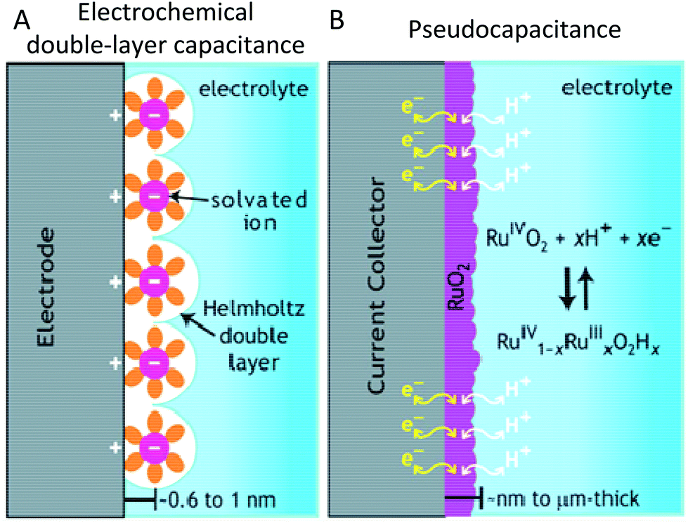 | ||
| Fig. 99 Schematic of charge storage in EDLCs via (A) electrochemical double-layer capacitance, where energy is stored by forming an EDL of electrolyte ions on the surface of conductive electrodes or (B) pseudocapacitance, where redox reactions occur close to the electrode surface (Adapted from ref. 1894). | ||
The way to optimize performance is by (i) maximising the electrode active surface areas; (ii) decreasing the electrode thicknesses; (iii) increasing the operating voltage window; (iv) using materials with high conductivity and/or high dielectric constant (the latter especially important for pseudo-capacitor electrodes).1885 A pseudo-capacitor, see Fig. 99b, is a supercapacitor containing at least one electrode material with redox reactions that occur close to the electrode surface.1892,1893
Apart from the mere optimization of the parameters involved in the process, one of the most crucial challenges in increasing performance is the poor mechanical and thermal stability of the materials used in current technologies, such as conductive polymers and metal oxides.1895 In fact, the uptake of ionic species in the charging/discharging process is usually accompanied by volume changes in the host electrodes.1844 The mechanical strain during these continuously repeated processes leads to cracking1844 and crumbling1844 of the electrode materials and loss of capacity over a few cycles.1844
GRMs can significantly change electrode and electrolyte properties and, consequently, their performance for energy storage and conversion. There are several potential advantages associated with the development of supercapacitors based on these nanomaterials. First, the use of thin layers of conductive TMDs, TMOs and graphene will reduce the electrode thickness and increase the surface area of the active units. Exfoliated TMO (or hybrids graphene-TMOs) are ultra-thin (capacitance and thickness of the electrodes are inversely proportional), conductive, with high dielectric constants.
The dielectric constant measures the extent to which a material concentrates electric flux. As it increases, the electric flux density increases. This enables objects of a given size, such as sets of metal plates, to hold their electric charge for long periods, and/or to hold large quantities of charge. Intercalation of ions between the assembled 2d flakes and within the thin layers could provide pseudo-capacitance. Moreover, the use of nanostructured thin layers of oxides in supercapacitor electrodes has the potential for enhanced volumetric capacitances (up to an order of magnitude higher than with the much less dense carbons currently used). The capacitance at an oxide electrode comprises both double layer and pseudocapacitance (Faradaic) contributions.1835 Both specific surface area (SSA) of the electrode material, and the potential for charge transfer with possible intercalation/de-intercalation are relevant variables controllable by tailoring the TMOs.
Recent works have shown the possibility to develop graphene-based supercapacitors with high performance, superior to existing supercapacitors based on activated carbon, see Table 7.
| Starting material | Specific surface area (m2 g−1) | Specific capacitance and notes | Ref. |
|---|---|---|---|
| a Although SSAs above 3000 m2 g−1 are higher than the SSA of ideal graphene, the measured SSA should be considered as an apparent or equivalent area, because the Brunauer–Emmett–Teller2344 method used for SSA determination is not applicable to microporous solids.1887 | |||
| RGO | 705 | EDLC ultracapacitors based on CMG-based carbon electrodes Specific capacitance of 135 and 99 F g−1 in aqueous KOH and organic electrolyte | 1667 |
| RGO | 3100a | Specific capacitance of 166 F g−1, corresponding volumetric capacitance of 60 F cm−3 | 1887 |
| RGO | 3523a | Specific capacitance of 231 F g−1; energy density ∼98 Wh kg−1 | 2343 |
| RGO | Volumetric capacitance of 206 F cm−3 | 1909 | |
| (1) Mesoporous Carbon capsules (MCCs) | 1500 | Specific capacitance MCCs: 134 F g−1 | |
| (2) Microwave exfoliated GO | Microwave exfoliated GO: 41 F g−1 | ||
| (3) RGO | RGO: 25 F g−1 (Supercapacitors with same ionic liquid electrolyte) | 1896 | |
| RGO/poly(ionic liquid) | N/A | Specific capacitance ∼187 F g−1 | 1888 |
| Electrolyzed GO suspensions with lithium perchlorate | N/A | Double layer supercapacitor with capacitance/surface area = 240–325 μF cm−2 104 to 1 Hz and a phase angle of −84 degrees. Used for AC line filtering | 1897 |
| MnO2 nanorods electrodeposited onto CNPs | N/A | Specific capacitance: 389 F g−1. Flexible, non-transparent, solid state capacitor | 1889 |
| RGO | 12.7 | Specific capacitance 210 F g−1 with 0.3 A g−1 discharge rate, or 170 F g−1, with 6 A g−1 discharge current. Conductivity of the RGO/PNF composite ∼5.5 × 10² S m−1 | 1898 |
| LPE graphene | N/A | Specific capacitance: 315 F g−1 | 1899 |
| Maximum power density ∼110 kW kg−1, energy density ∼12.5 Wh kg−1 | |||
| RGO | 107 | Specific capacitance: 31 F g−1 (24.5 F g−1 after 1000 cycles) | 1900 |
| Energy density 30.4 Wh Kg−1 (RGO-MnO2) | |||
| Hybrid electrode graphene/super-P/PTFE | N/A | Specific capacitances 100–250 F g−1 at a high current density of 1 A g−1 Energy density 85.6 Wh kg−1 at 1 A g−1 at RT, 136 Wh kg−1 at 80 °C | 1905 |
| RGO | 320 | Specific capacitance of 205 F g−1, 170 F g−1 (∼90%) after 120 cycles. Energy density of 28.5 Wh kg−1 in KOH aqueous electrolyte solution | 1890 |
| RuO2− graphene sheets | N/A | 570 F g−1 (97.9% retention after 1000 cycles) | 1901 |
| Energy density 20.1 Wh kg−1 at 100 mA g−1 or 10000 Wh kg−1 at 4.3 Wh kg−1 |
|||
| Ni(OH)2 grown on graphene sheets | N/A | 1335 F g−1 at 2.8 A g−1 and 953 F g−1 at 45.7 A g−1 | 1902 |
| Ti3C2 | N/A | 300 F cm−3 | 1097 |
The EDLC energy density is determined by the square of the operating voltage and the specific capacitance (capacitance per unit mass F g−1 or volume F cm−3) of the electrode/electrolyte system.1895 The specific capacitance in turn is related to the electrode's SSA accessible by the electrolyte, its interfacial capacitance (F cm−2) and, in the case of specific capacitance, the electrode material density.1903,1904 Graphene-based supercapacitors have been developed with energy density comparable with that of Ni metal hydride batteries.1905 In particular, exploiting microwave expanded graphite oxide (MEGrO) activated by KOH, i.e. activated MEGrO (a-MEGrO),1887 an interfacial capacitance of 22 μF cm−2 was achieved.1906 Aerosol spray drying of GO with a hierarchical pore 3d structure yielded a specific capacitance ∼103 F cm−3 in a IL electrolyte.1907 Higher specific capacitance values were obtained exploiting a-MEGrO made by vacuum filtering (177 F cm−3 in IL electrolyte).1908 Capillary compression of RGO gave ∼206 F cm−3 in IL.1909
Intercalation of cations (e.g., Na+, K+, NH4+, Mg2+, and Al3+), from aqueous salt solutions between Ti3C2 MXene was reported.1097 A capacitance in excess of 300 F cm−3, a value that is much higher than that achieved by porous carbons, was demonstrated.1097
A major challenge is to bridge the performance gap between Li-ion batteries and EDLCs by developing technologies that can take advantage of both devices. Hybrid supercapacitors,1910 HSC, offer a solution to this problem by combining a capacitive electrode (power source) with a Li battery-like electrode (energy source). The present level of energy/power densities in HSC, as well as their safety, cyclic life and charging performance, are far below the levels required to power demanding systems. The aim is to address these challenges simultaneously by fabricating the next generation HSC based on graphene- core/metal oxide-shell nanostructured electrodes. The key step will be the alignment of graphene sheets to form a hierarchically layered structure on the microscopic level. Two strategies can be followed for the production of highly-aligned graphene sheets. The first can rely on MWCVD, while the second may involve layer by layer solution-based deposition. The vertically aligned graphene sheets would have several advantages over random dispersions: (1) much higher electrical and thermal conductivities; (2) larger surface area for interaction with the active material, Li ions and electrolytes; (3) better control of volume expansion, etc., all of which give rise to enhanced electrochemical properties and safe operation. The specific targets will be (a) precise synthesis and full characterisation of aligned graphene core/metal oxide shell architectures; (b) establishing correlations between the compositional, structural, electrical and ionic properties of core/shell electrodes; (c) developing high energy density, superior power capability and stable lifespan HSCs devices.
For supercapacitors future investigations should also include activated GO, its surface is covered (or decorated) with chemicals, e.g. potassium hydroxide,1887 with controlled GO sheet curvature, controlled mesoporous electrodes combining GO sheets with CNTs, graphene-like structures with controlled and highly uniform pore sizes (TiC chlorination derived process). Upstream support activities need to focus on systematic exploration on how layer spacing affects capacitance. NMR characterization will also help identifying charging mechanisms and the role of different functional groups. These development should lead to more robust supercapacitors able to operate in more demanding conditions (−30 to 100 °C).
The development and implementation of a new generation of supercapacitors based on GRMs should target: (1) power electronics systems to improve operation efficiency, in particular electrical power delivery and propulsion systems (minimization of energy losses, power quality improvement, DC power transmission, etc.).; (2) power electronics systems for efficient renewable energy sources and integration in power grid; (3) power grid equipment to provide efficient operation in power production system and “smart grid”; (4) electric vehicles, in particular electric buses and commercial electric vehicles employing energy efficient electric & hybrid vehicle propulsion systems; (5) remote, GSM based, systems to monitor and control power electronics controlled drives, etc.; remote control and monitoring systems of distributed industrial objects based on Wide Area Networks (Internet/Extranet) and wireless communication (GSM).
10.3. Fuel cells and hydrogen storage
A fuel cell is a device that converts the chemical energy from a fuel into electricity through a reaction with oxygen or another oxidizing agent.1912 Fuel cells are different from batteries and supercapacitors in that they require a constant source of fuel and oxygen to run, but they can produce electricity for as long as these inputs are supplied. There are many types of fuel cells, such as proton exchange membrane (PEMFCs)1913 (see Fig. 100), solid oxide fuel cells,1914 molten carbonate,1915 phosphoric acid,1916etc., but they all consist of an anode (negative side), a cathode (positive side) and an electrolyte that allows charges to move between the two sides of the fuel cell. Electrons are drawn from the anode to the cathode though an external circuit, resulting in a current.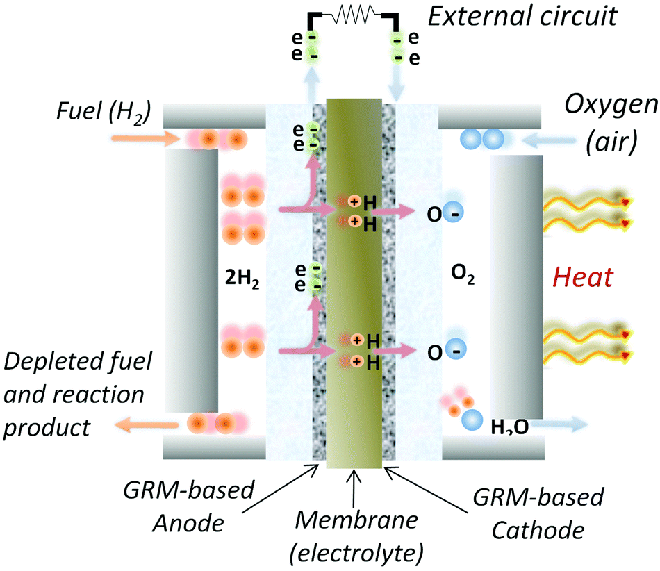 | ||
| Fig. 100 Proton exchange membrane fuel cells.1911 Fuel (e.g. H2) channelled from one side of the fuel cell is split by catalyst (e.g. graphene electrode) into H+ ions and e-. Electrons generate a current in the external circuit and they combine with H+ and the oxidant (O2) at the cathode forming water and heat. Adapted from ref. 1841. | ||
Fuel cells can have numerous applications, in vehicles, power backup systems, mobile phones, smart textiles (embedding digital computing components and electronics), providing a durable supply of electricity. The integration of fuel cells into flexible electronics needs flexible films as electrodes. In this context, graphene can play a role in replacing currently used materials, such as expensive noble metals Pt, Au, Ru, and their alloys. Indeed, these materials are the most common cathode materials for the oxygen reduction reaction (ORR)1901,1917–1920 in fuel cells.
The target is to develop novel inexpensive fuel cell catalyst exploiting GRMs.1921,1922Ref. 1921 reported that graphene performs better than a commercial Pt catalyst in terms of ORR. GRM are also promising materials as electro-catalyst, e.g. in PEMFCs, for the electro-oxidation of fuel1923 at the anode. Ref. 1924 demonstrated that graphene-supported Pt and Pt–Ru NPs have enhanced efficiency for both methanol and ethanol electro-oxidations with respect to Vulcan XC-72R carbon black, which is the widely used catalyst.1841Ref. 1925 demonstrated that RGO gives rise to modification to the properties of Pt cluster electro-catalysts supported on it. Pt/graphene hybrid electro-catalysts were reported with an higher activity for methanol oxidation compared to Pt/carbon black.1925 The edges of LMs, such as MoS2 and WS2, were shown to be active catalytic sites,1926 thus promising for the hydrogen evolution reaction (HER) in hydrogen fuelled fuel cells.1927
Hydrogen is currently considered one of the most promising fuels for cells,1928 since its specific energy exceeds that of petroleum by a factor of three1929 and the product of its combustion is water vapour. However, hydrogen is not an energy source, but a secondary energy carrier. It means that hydrogen must be produced, and the amount of energy needed in the production process is subsequently released during its use in fuel cells. Consequently the advantage of hydrogen for energy must be carefully considered with respect to other carriers, such as electricity. In light of this, the issue of finding ways and materials for efficient hydrogen storage assumes a primary importance.
During the past decades several means for hydrogen storage were considered.1930–1933 The efficiency of storage is usually evaluated by the gravimetric density, GD, i.e. the weight percentage of hydrogen stored relative to the total weight of the system (hydrogen + container), and the volumetric density, VD, i.e. the stored hydrogen mass per unit volume of the system.1934 The 2015 Department of Energy-USA (DoE) targets locate “good” storage systems at a level of 5.5% GD and 0.04 kg m−3 VD, which would correspond to an usable energy per mass of 1.8 kWh kg−1.1935 The GD vs. VD diagram for several hydrogen storage systems, including graphene-based ones, is shown in Fig. 101. The diagram includes gaseous and liquid forms, solid-state systems in the form of hydrides1936,1937 including MgH2,1938–1941 and in systems obtained by nanostructuring Mg into nanocrystals.1942 Sodium alanate, NaAlH4, is also extensively studied as one of the most promising solid-state hydrogen-storage materials.1936,1943 Another class of recently considered compounds are hydrocarbons and N- B- hydrides.1944–1946 These satisfy the GD and VD requirements, and require chemical reactions to control hydrogen charge/discharge.
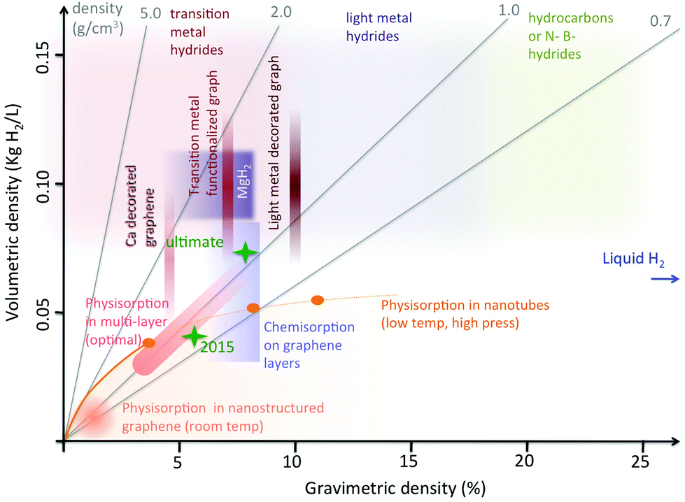 | ||
| Fig. 101 Gravimetric vs. volumetric density diagram for several hydrogen storage systems including the graphene-based ones. The orange line represents the optimal relation for physisorption in CNTs (dots correspond to different sizes). The line tends to the value of liquid hydrogen for large CNTs. In general, nanostructured physisorption based graphitic systems occupy the area below this line. The oblique shaded strip represents the optimal physisorption within FLGs with spacing nearly double than graphite (and density ∼ one half). Different storage densities in this case correspond to different pressure and T. The vertical dark red strips represent adsorption in decorated or FG. These systems have been mostly studied at the level of a single layer, for this reason only GD is well defined, while the VD range was estimated considering variable inter-layer spacing 2–4 times that of graphite.1974 The same criterion was used to estimate VD for chemisorption in FLGs (blue rectangle): in this case GD has a sharp right edge, corresponding to the maximum loading with 1:1 stoichiometry of C and H (∼8%).1974 The storage properties of systems based on materials different from graphene (different metal hydrides (including MgH2), hydrocarbons, N- and B-hydrides) are also reported as shaded areas in red, violet and green. The DOE targets (for 2015 and ultimate) are indicated with green stars. The constant density lines are in grey. Adapted from ref. 1974. | ||
Graphene offers several potential advantages when considered as a medium for hydrogen storage. It is stable and robust, therefore can be transported for long distances. At the same time it is mechanically flexible, enabling new charging/discharging strategies at RT that exploit the dependence of hydrogen–carbon binding on local curvature,1947 see Fig. 102. It was theoretically suggested that CNTs behave similarly to curved graphene:1947 curvature favors physisorption (a process in which the electronic structure of atoms or molecules is barely perturbed upon adsorption) (into concavities)1948 and chemisorption (a process where the electronic structure of bonding atoms or molecules is changed and covalent or ionic bonds are formed) (on convexities).1949,1950 In particular it was shown that for small diameter (0.5–0.6 nm) CNTs the chemisorption barrier can become negligible,1949,1950 favouring the spontaneous molecular hydrogen chemisorption. This should also happen on small diameter fullerenes. There is also some theoretical work on the physisorption in the interstitial volumes of nanotubes bundles,1951 where hydrogen in metal-intercalated nanotube bundles is substantially enhanced compared with adsorption onto pure CNTs.1951 What, however, is new and unique to graphene, is the possibility of manipulating the local curvature, consequently controlling the hydrogen uptake. This is not possible with CNTs or fullerenes. In perspective, assuming that methods for the production of bulk graphene samples will improve with time, graphene's flexibility and unique electronic properties could enable new approaches for hydrogen storage, such as the integration of hydrogen-storage modules into flexible and light, all-graphene-based devices. It is also possible that integration of graphene into the above-mentioned hydrogen storage materials might offer additional routes for the realization of optimized hybrid tanks.
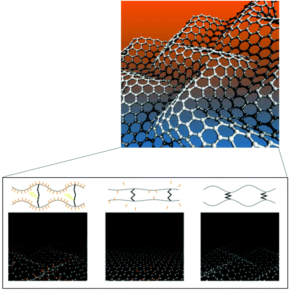 | ||
| Fig. 102 Corrugated graphene sheet by lateral compression and illustration of controlled hydrogen adsorption and release by curvature inversion.1947 | ||
Hydrogen can be adsorbed on graphene in two different ways: either by physisorption, i.e. interacting by VdW forces, or by chemisorption, i.e. by forming a chemical bond with the C atoms. Physisorption usually happens with hydrogen in molecular form.1952 It was shown that in the most favourable conditions (high pressure and low T) H2 can form a uniform compact monolayer on the graphene sheet, corresponding to GD = 3.3%1953 (doubled if two sides are considered). The VD depends on the possibility of compacting graphene sheets in multi-layers, 3d assemblies or nano-structures of graphene.
In multi-layers, calculations based on hybrid post-Hartree–Fock/empirical potentials and including quantum treatment for hydrogen,1952,1954 indicate that both GD and VD depend on the inter-layer separation, with highest values for an interlayer separation of 6–8 Å.1952 Monte Carlo simulation of an artificial 3d structure composed of graphene layers placed at an interlayer distance of 12 Å and stabilized by CNTs inserted perpendicularly to the graphene planes,1955 showed GD up to 8% at low T and high pressure, decreasing by an order of magnitude at room conditions, but raising up to 6% at RT and ambient pressure after doping the pillared structure with Li cations.1955 Experimentally, it was shown that such a layered structure can be realised by using GO and the interaction between hydroxyl groups and boronic acids1956 (i.e., an aryl or alkyl substituted boric acid containing a carbon–boron bond) with a predicted GD ∼6% at 77 K at a pressure of 1 bar.
The enhancement of VdW interaction1957 can be similarly postulated in any hollow graphene nano-structure. E.g., an empirical estimate of the maximal VD vs. GD relation of hydrogen physisorbed in CNTs can be obtained assuming a level of compression similar to that of liquid H2 and a full occupation of the cavity. Experimentally, however, the best reproducible results yield GD ∼ 1% at a pressure of 120 bar at RT.1958
Molecular hydrogen adsorption in graphene-like flakes obtained by chemically reducing exfoliated GO has been studied,1959 leading to a molecular hydrogen adsorption of 1.2% at 77 K and a pressure of 10 bar and 0.68% and ambient pressure.1959 A GD ∼ 2.7% at 25 bar and RT was reported in GO after ultrasonic exfoliation in liquid.1960
Chemisorption processes may reach GD = 8.3%, i.e. even larger than the “ultimate” goal of DOE. This corresponds to the formation of a completely saturated graphene sheet, with 1:1 C vs. H stoichiometry, i.e. “graphane”, whose stability was first hypothesized in a DFT-based theoretical study,1961 and subsequently studied in experiments.33Ref. 33 has shown one-side hydrogenation and its reversibility by thermal annealing. The chemisorption of atomic hydrogen is a favourable process: accepted values for H binding energy and chemisorption barriers are ∼0.7 and ∼0.3 eV,1953,1962–1967 STM experiments have focussed on atomic-scale imaging of adsorption and clustering of hydrogen atoms on graphite.1968–1971 Atomic hydrogen absorption on graphene grown on SiC was also investigated by STM,1972,1973 showing formation of dimer structures, preferential adsorption of protruding graphene areas and clustering at large hydrogen coverage.1972,1973
As in the case of physisorption, VD depends on the possibility of building compact structures with graphene (or graphane) sheets. Considering inter-layer spacing from 2 to 4 times that of graphite, it is possible to obtain VD values from 0.03 to 0.08 kg H2 L−1, which fit and exceed the DOE goals. However, chemisorption of molecular hydrogen on graphene presents rather high barriers ∼1.5 eV,1975 requiring the dissociation of H2 (dissociative adsorption). Analogously, the desorption of hydrogen (associative desorption) has a barrier of similar height. This makes H storage on graphene stable, but poses problems in the release phase. These problems are in common with other storage media based on hydrocarbons, or in general on chemical adsorption.
Given its peculiar nature of 2d extended system, graphene gives the possibility of exploiting its mechanical properties to perform H release. It was proposed theoretically1947 that graphene's curvature can be used to control uptake and release of H. It was calculated by DFT1947 that, when a graphene sheet is rippled, hydrogen preferentially binds on convex areas. This site selective adsorption of atomic hydrogen was experimentally verified by STM on convexly warped regions of SLG grown on SiC(0001).1976 This showed that, at low coverage, hydrogen is on convex areas of the graphene lattice, while no hydrogen is detected on concave regions.
Based on these results, one could envisage that, if the curvature of the sheet is inverted and convexities are transformed in concavities, hydrogen might spontaneously release, even at RT.1947 The large variation of H binding energy makes chemisorption a favourable process on convex sites, and hydrogen release a favourable process on graphene concave sites, offering a new route towards hydrogen storage/release.
GRMs might also be exploited for the production of clean fuels, such as H2, in a cost effective, renewable process. Photocatalytic splitting of water into H2 and O2 using semiconductor-based heterogeneous systems could be a viable method for H2 production.1977,1978 A major limitation is the lack of stable semiconductor photocatalysts that can carry out the water splitting in the visible region of the solar spectrum. Stable efficient and visible light driven photocatalysts might be achieved by using chemically derived graphene as a support for chalcogenide nanocatalysts. Graphene will serve several purposes. Its layered structure might not only suppress the semiconductor particle growth, but also act as an electron collector and transporter to lengthen the lifetime of the photo-generated charge carriers, see Fig. 102.
10.4. Graphene solar cells
The direct exploitation of solar radiation to generate electricity in PV devices is at the centre of an on-going research effort. Si is by far the most widely used absorber1979 and currently dominates the PV market,1979 with energy conversion efficiency (η) up to ∼25%.1980η is defined as η = Pmax/Pinc, where Pinc is the incident power and Pmax = VOC × ISC × FF, where VOC is the maximum open-circuit voltage, ISC is the maximum short-circuit current and FF is the fill factor, defined as FF = (Vmax × Imax)/(VOC × ISC), with Imax and Vmax the maximum current and voltage.1981Despite significant development over the past decades,1982 the cost1980,1982 of crystalline Si-based solar cells, often referred as 1st generation solar cells,1979 is still a bottleneck for the implementation of solar electricity on large scale. The development of new materials and concepts for the PV devices is thus fundamental to increase efficiency, especially for mobile applications with limited surface area.
Thin film solar cells such as a-Si,1983 cadmium telluride (CdTe),1984 copper indium gallium diselenide (CIGS)1985 and thin film crystalline Si are known as second generation PVs, because they are based on thin-film technology. The development of thin film solar cells is driven by the potential costs reduction.1986
An even cheaper and versatile approach relies on the exploitation of emerging organic PV cells1987 and DSSCs.408 They can also be manufactured by a R2R process,1988 even though they have lower η. An organic photovoltaic cell relies on polymers for light absorption and charge transport.1987 It consists of a TC, a photoactive layer and the electrode.1987 DSSCs use an electrolyte (liquid or solid) as a charge-transport medium.408 This solar cell consists of a high-porosity nanocrystalline photoanode, comprising TiO2 and dye molecules, both deposited on a TC.408 When illuminated, the dye captures the incident photon, generating e–h pairs. The electrons are injected into the TiO2 conduction band and then transported to the CE.408 Dye molecules are regenerated by capturing electrons from the electrolyte.
Another class of solar cells, called meso-super-structured solar cells (MSSCs) was proposed in ref. 1989. These are based on organic halide perovskite LMs (e.g. CH3NH3PbX3 where X is Cl, Br, I, or their combination) as photosensitizer1989–1992 and an organic hole-transport material.1990 An efficiency of 20.1% was recently reported,2341 a very promising value, considering that the device structure can still be further optimized. However, these LMs may not satisfy sustainability requirements because of their lead content.
Graphene, thanks to its mechanical, electronic and optical properties, can fulfil multiple functions in PV devices: as TC window, antireflective layer, photoactive material, channel for charge transport, and catalyst.1841 GTCFs can be used as window electrodes in inorganic,1993 organic710,1994 and DSSCs.1788 The best performance has been achieved to date in graphene/n-Si Schottky junction solar cells with η = 8.6%.1995 The GTCFs was doped with bis(trifluoromethanesulfonyl)-amide[((CF3SO2)2NH)] polymer.1995 Higher η ∼ 10.34%1996 was achieved in an organic/Si cell exploiting GTCF doped with HNO3, with potential for having work function tuning capability, important to control the contact resistance.1997
Charge transport and collection have also a fundamental role in organic PV (OPVs). In a poly-3-hexyl thiophene (P3HT)/phenyl-C61-butyric acid methyl ester (PCBM) solar cell both donor (P3HT) and acceptor (PCBM) materials are in direct electrical contact with the cathode (back electrode) and anode (ITO) electrodes, leading to carriers recombination.1998 This negative effect can be reduced using electron blocking and hole transport layers (HTLs), usually deposited on top of ITO.1998,1999 GO dispersions were also used in bulk heterojunction PV, as electron-acceptors,2000,2001 with η ∼ 3.5% (ref. 1998). Higher η with respect to GO were achieved with the use of RGO as HTL. Ref. 2002 demonstrated η = 3.98%, superior to PEDOT:PSS (η = 3.85%). Hybrid structures (e.g. GO/SWNTs) were also investigated as HTL.2003 The addition of a small amount of SWNTs in the GO layer significantly improved the devices’ FF.2003 Indeed OPVs fabricated with GO/SWCNTs as HTL have shown higher performance (η = 4.10%) compared to devices using PEDOT:PSS (η = 3.28%). GQDs can also be efficient HTLs for OPVs, with η = 6.82%,2004 showing longer lifetime and more reproducible PV performances with respect to PEDOT:PSS-based cells.2004Ref. 2005 reported that the short circuit current of P3HT:PCBM solar cells is enhanced by ∼10% by the addition of graphene produced by LPE, with a 15% increase in the photon to electric conversion efficiency. The addition of graphene flakes to the P3HT:PCBM blend also improves the balance between electron and hole mobilities with respect to a standard P3HT:PCBM solar cell.2005
GRMs have also been proposed as photosensitizers,1331 to absorb the incident light and convert it into an electrical current.1979 For OPVs, the key requirements of a photosensitizer are: (i) ability to absorb light over a wide energy range;1331 (ii) high carriers mobility;1331 (iii) thermal and photochemical stability;1987 (iv) efficient charge separation between donor/acceptor materials.1987 Simulations based on equivalent electrical circuits for OPVs indicate that η ∼ 12% should be possible with graphene as photosensitizer.2006
Graphene can cover an even larger number of functions in DSSCs, as for SWNTs,2007 but without the need for sorting.2007 Other than as TC window,1788 it can be incorporated into the nanostructured TiO22008 or ZnO2009 photoanode to enhance the charge transport rate, preventing recombination, thus improving the internal photocurrent efficiency, i.e. the fraction of absorbed photons converted into electrical current. η ∼ 7%, higher than with conventional TiO2 photoanodes in the same conditions, was reported.2008 GQDs with tuneable absorption were designed, and shown to be promising photoactive materials in DSSCs.956 Further work is required for optimum adsorption to the TiO2 NPs, by covalently attaching binding groups in order to improve the charge injection. Ref. 2010 seems to have found the right strategy to efficiently introduce in FLG flakes, prepared via solution processing, TiO2 NPs, and used them as electron collection layer in perovskite-based MSSCs achieving η = 15.6%. This is the highest η amongst graphene-based solar cells to date (see Fig. 103), thanks to the superior charge-collection of the FLG-TiO2 composite, with respect to the bare TiO2 (η = 10%).2010
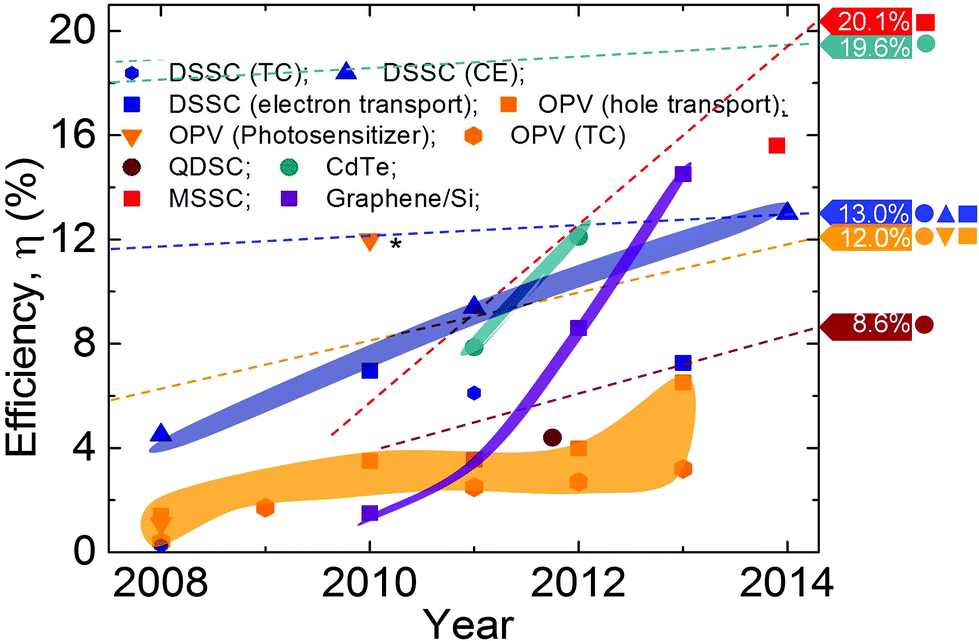 | ||
| Fig. 103 Solar energy conversion efficiency of GRM-based PV devices. Colors define different classes of PV devices: cyan, CdTe;2028 red, MSSCs;2010,2029 purple, graphene/Si;1993,1995,2030 blue, DSSCs;1788,2008,2018,2019,2031 orange, OPVs;915,2006,2101 wine, quantum dots solar cells-QDSCs.2032 Symbols are linked to different functions of the GRMs for each PV device: blue rhombuses,1788 TC; blue triangles,2018,2021 CE; blue squares,2008,2009 electron transport in DSSCs. Closed areas define different GRM functions in OPVs (orange area) and DSSCs (blue area). The data on the right axis refer to state-of-the-art PV efficiency based on non-GRM materials,2033 with the dashed lines representing their timeline [data taken from ref. 1980]. The asterisk refers to a theoretical work for OPV.2006 | ||
Another option is to use graphene, with its high SSA,28 as substitute for the Pt CE. Several groups have used carbonaceous materials at the CE: activated carbon,2011 CNTs,2012–2015 hard carbon spherules2016 and graphite.2016 Graphene nanoplatelets2017,2018 and GO2019–2022 have also been proposed as CE. E.g., a hybrid poly(3,4 ethylenedioxythiophene): poly(styrenesulphonate)PEDOT:PS/GO composite was used as CE, getting η ∼ 4.5%,2021 comparable to η ∼ 6.3% for a Pt CE tested under the same conditions,2021 but now with a cheaper material. Nitrogen-doped GNPs were exploited in DSSCs reaching η = 9.05%, outperforming Pt (η = 8.43%).2023
Inorganic LMs such as TMO, and metal carbides, nitrides and sulphides were also used as CE in DSSCs.2024Ref. 2024 used MoS2 and WS2 CE, with the I3−/I− redox couple, achieving η = 7.59% and 7.73%, respectively, close to those achieved in the same work with Pt. Ref. 2024 outperformed standard Pt CEs, both with MoS2 (4.97%) and WS2 (5.24%) using a disulfide/thiolate (T2/T−) redox couple. Hybrid graphene/inorganic LMs, such as MoS2–graphene, were used as CE in DSSCs with η = 5.81%.2025 The state of the art in GRM-based solar cell is summarized in Fig. 103.
GRMs might be implemented in different types of solar cells. This may facilitate their use in a variety of applications, ranging from mobile devices, printed electronics, building technologies, etc. E.g., in mobile phones, apart the improvement of energy storage devices, with reduced size and weight and with longer and more stable performance, the development of more efficient energy harvesting methods could lead to energetically autonomous devices. Graphene maintains its properties even under extreme bending and stretching. This is ideal for its integration in polymeric, rigid and flexible substrates, for the integration in smart windows and other building components. This increases fabrication flexibility, in addition to having economic advantages.
The efficient electric field concentration of MNPs can increase the light-harvesting capacity of graphene by more than an order of magnitude.446 A multilayer structure solar cell (see Fig. 104) can be envisaged, with graphene and QDs to achieve total light absorption, thus higher efficiency. Another option is a multilayer structure heterojunction, based on QDs (MoS2, WS2, CdS, PbS, ZnS, etc.) alternating with graphene conductive layers, or coupling a standard DSSC with a Graphene/MoS2 (or WS2) tandem solar cell. The aim is to overcome the η of state of the art solar cells extending it beyond the Shockley–Queisser2026 limit (i.e. the maximum theoretical efficiency of a p–n junction solar cell) by using multiple sub-cells in a tandem device. Ideally, the sub-cells would be connected optically and electrically and stacked in band-gap decreasing order. This configuration shifts the absorption onset of the complete device towards longer wavelengths. In addition, high-energy photons are converted more efficiently since thermalisation losses of the generated e–h pairs are reduced with the graded band gap structure. E.g. in a series-connected double-junction device, the ideal optical band gaps are ∼1.6–1.7 eV for the top cell and ∼1.0–1.1 eV for the bottom cell, which extends the efficiency limit to ∼45%.2027
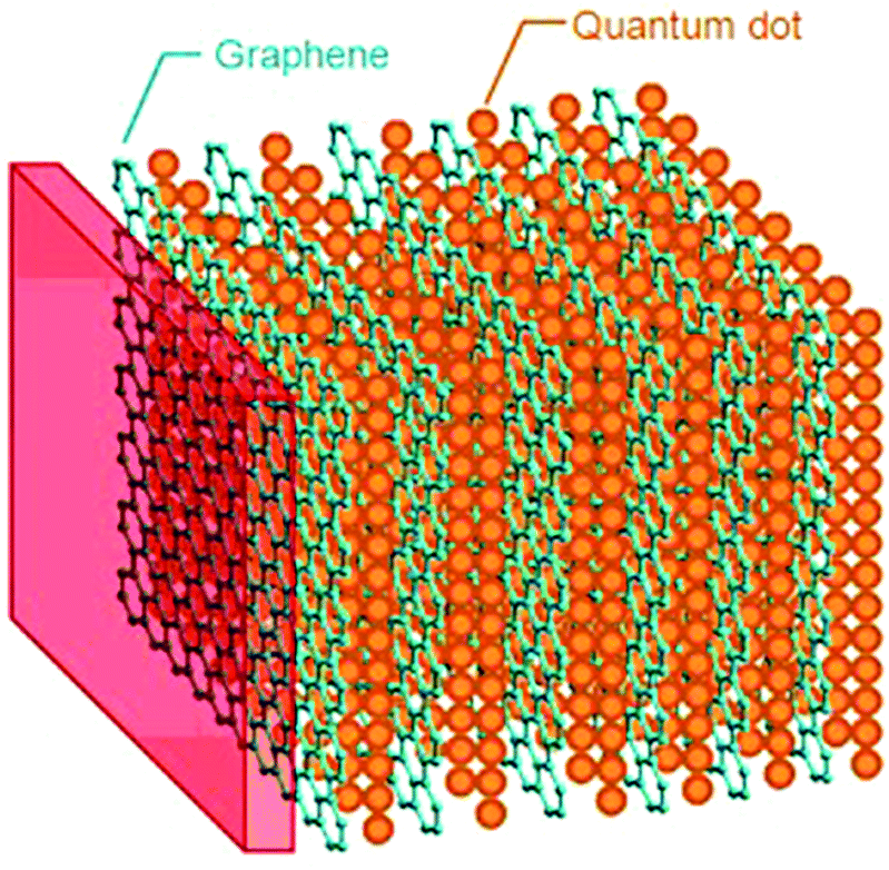 | ||
| Fig. 104 Multilayer solar cell composed of alternating stacked SLG and quantum dots. | ||
Another possibility is to assemble hybrid graphene/nanodiamonds,2034,2035 motivated by the properties of both materials, and possible interactions between sp2 and sp3 carbon.2036 The <111> diamond surface could form an ideal interface for heteroepitaxial graphene, with ∼2% mismatch. The armchair diamond rings on the <111> surface can be interfaced to the 6-membered C rings of graphene. There are several impacting interests in these interfaces. Un-doped nanodiamond could serve as gate insulator. A controllable functionalization of nanodiamond may be used to tune graphene's μ and work function other than the optical properties. This might be achieved by coupling graphene, using organic chemistry routes via linkers with functional properties, to nanodiamond. In these solar cells, conductive B-doped nanodiamond would serve as anode, while graphene would be the cathode. If donor–acceptor organic dyes are used for such interfacing, the proposed full carbon structure would have effective charge transfer from the HOMO of the organic dye to the diamond valence band, and in a reversed process on the graphene/LUMO side.
Another approach relies in the use of chemically synthesized GNRs and/or GQDs sensitizers in solar cells. GQDs have been synthesized with molar extinction coefficients (∼1 × 10⁵ M−1 cm−1,956 ∼one order of magnitude larger than inorganic dyes (e.g. ruthenium complexes),956 commonly used in DSSCs) and absorption edge beyond 900 nm.956
10.5. Thermoelectric devices
Thermoelectric (TE) devices, i.e. solid-state devices (Fig. 105) that generate electricity from a T gradient,2037 are ideal to recover waste thermal energy.2037 Inorganic layered compounds are promising as thermoelectric materials, to extract electrical energy from a T gradient (e.g. waste heat).2037 Such materials need high Seebeck coefficient (S), high σ and low κ.2037,2038 These properties are found in some LMs such as Bi2Te3.111 The effectiveness of a TE device is assessed in two ways: by its Carnot efficiency (i.e. the maximum efficiency possible for converting a given amount of thermal energy into work) and by a material-dependent factor called the TE figure of merit zT (105); zT = TS2σ/k,2038 where S is the Seebeck coefficient, T the temperature, κ the thermal conductivity and z = S2σ/k.2037,2038 Thus, TE materials require high S and σ values, and low κ.2039 In order to optimize zT, phonons must experience a high scattering rate, thus lowering κ2039 (i.e. as in a glass) while electrons must have little scattering, maintaining high σ (i.e. as in a crystal).2040 It was shown that κ of Bi2Te3 can be suppressed by reducing the grain size.2041 The ideal way to do this would be LPE.38 Thus LPE-Bi2Te3 devices could be made with figure of merit zT > 1.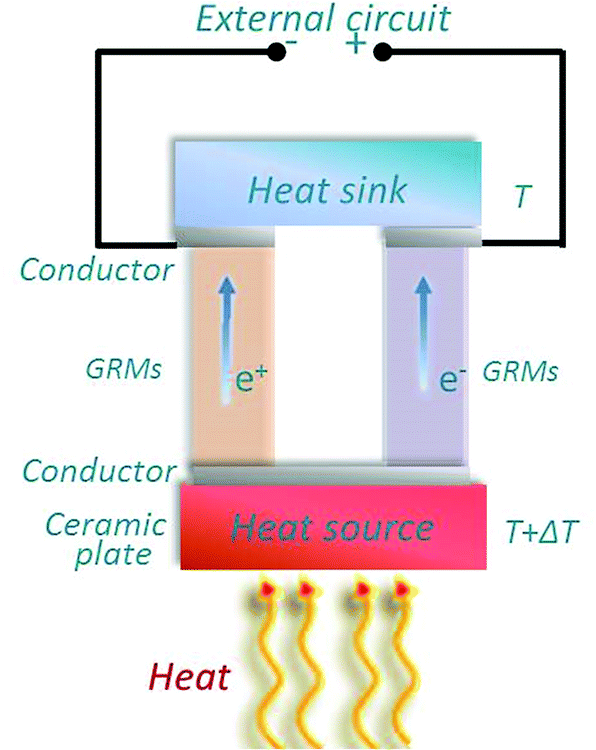 | ||
| Fig. 105 Schematic illustration of power generation in a TE device based on Bi2Te3 LMs or GNRs. A T gradient, ΔT, causes charge carriers in the material to diffuse, resulting in current flow through the external circuit. Adapted from ref. 1841. | ||
Many LMs have high S and low κ.111 The low σ generally means they are unsuited to thermoelectric applications. However, since LMs can be exfoliated in liquids, it could be possible to blend them with nanoconductors, such as CNTs or graphene. This may increase σ, while retaining S.2037 The challenge will be to keep κ at low values. To achieve this it is key to understand the physics of thermal transport in nanostructured disordered networks.
Graphene has high σ74 but also high κ,2042 a combination that it is not ideal for TE devices. However, it is possible to tailor the thermal transport properties of graphene by nano-structuring techniques, such as defects2043 and isotope2044 engineering, edge roughness2043 or introducing periodic nano-holes.2045 The combination of geometrical structuring, GNRs with predefined geometries,320 and isotopically modified graphene with 13C2044 can reduce κ by up to two orders of magnitude with respect to pristine graphene.2046Ref. 2046 estimated that zT up to 3.25 can be achieved exploiting GNRs having a chevron-like geometry.2046
10.6. Nanogenerators
Self-powering devices are a new paradigm in nanotechnology and green energy for sustainable self-sufficient micro/nano-systems, of critical importance for sensing, medicine, infrastructure/environmental monitoring, defense technology and personal electronics.2047The combination of mono-atomic thickness with high rigidity (Young modulus 1 TPa) and maximal strength (130 GPa),18 as well as unique optoelectronic995 characteristics, makes graphene a candidate for NOEMS (nano-optoelectromechanical systems) energy harvesting nanodevices (nanogenerators – NGs), which efficiently convert the energy from environmental sources, such as ambient noise or electromagnetic radiations (from RF to visible wavelength), to mechanical vibrations. This would enable mechanical compliances and resonant frequencies matching the energy levels and characteristic frequencies of non-explored energy sources arising at the nanoscale. When the energy source is noisy, non-linear MEMS with a broadband or a low frequency spectrum can be convenient as energy harvesters, based on the mechanical non-linearities of suspended GNRs.
Particularly interesting is the merging of energy harvesting and optoelectronic concepts and technologies, when envisaging the enhancement of light to nanomechanical vibrations conversion on a NOEMS device by using the higher optical absorption of doped or nanopatterned1578 graphene nanostructures.
Other NGs2048 exploiting piezoelectric,2049,2050 triboelectric2051,2052 and pyroelectric2053 effects have been investigated as efficient energy harvesting systems from the living environment.2047 A complete, flexible, and integrated system capable of harvesting and storing energy from the natural contractile and relaxation motions of internal organs such as heart, lung, and diaphragm was recently demonstrated with efficiency of ∼2%.2054
Nanogenerators integrated with graphene films were shown to possess outstanding mechanical and optical properties, thus offering unique benefits in high-performance flexible and transparent devices.2055Ref. 2055 demonstrated how all device components, including piezoelectric (PZT) materials and graphene electrodes, can be printed onto a plastic substrate, using a low T transfer process.
The resulting graphene-based PZT exhibited good mechanical bendability, Tr and simple device design, compatible with conventional batch fabrication steps.2055 The output power of the graphene-based PZT efficiently powered commercially available electronic components (e.g. LCDs and LEDs) in a self-powered mode, without any external electrical supply.2055 These results are encouraging in view of further development of graphene-based harvesting systems, particularly for applications that require flexibility and semi-transparency.
The timeline for the energy applications is shown in Fig. 106. The main targets are: 3 years: Pristine and functionalized GRMs for composites and intercalated compounds; Processing of GRMs for PV wet technology. 3–7 years: High capacitance GRM-based mesoporous electrodes; PV electrodes and absorbers. 7–10 years: flexible PV cells; Light electrical and hydrogen storage systems.
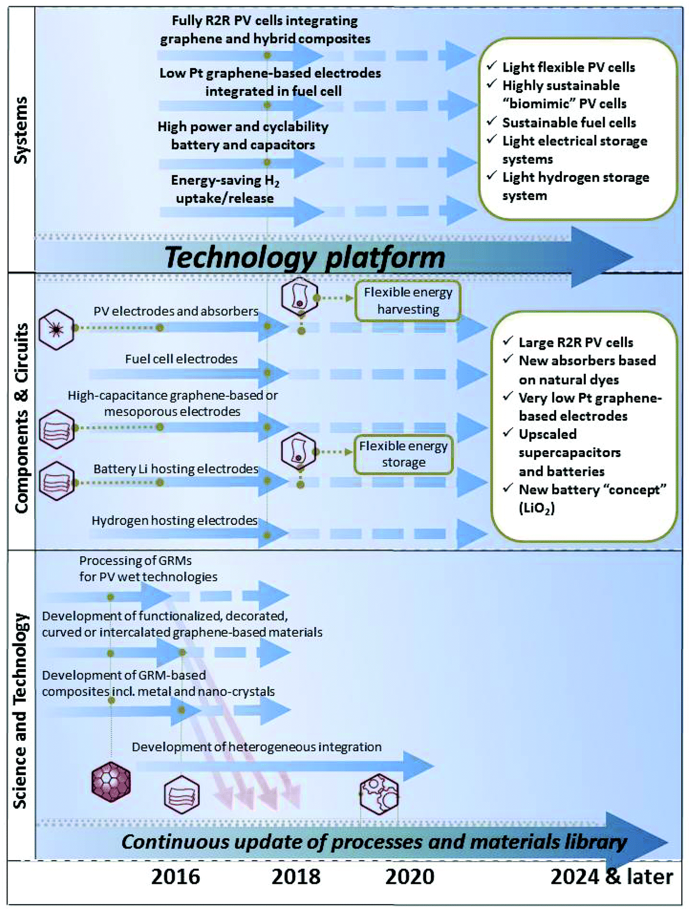 | ||
| Fig. 106 Energy applications timeline. The white rectangles summarize the main targets to be achieved in a timeframe of 10 years. | ||
11. Composites
The properties of graphene can be exploited for applications where, rather than a monolayer on a substrate, large quantities are processed from solution or melt to be included in bulk materials, like polymers.2056 These applications require low cost, high-processability in solvents and polymers and tuneable chemical properties.An advantage of graphene over other nanomaterials is that it can be produced either by bottom-up assembly of smaller atoms and molecules or top-down exfoliation of graphite stacks. Unlike CNTs, graphene can be produced on ton scale2057 without high T and metal catalysts, allowing cheap production for different large scale applications.2058
Graphene–based solutions may be used for antistatic, EMI shielding, conductive inks, and gas barrier applications. In principle, the production technology is simple and developed with most of the graphite mining companies having programs on LPE graphene.2059 Major developments should be made in the area of chemical derivatives of graphene in order to control electrical conductivity and optical properties of the final products.
Graphene, being an inert (unreactive under ambient conditions) material,2060 can also act as a corrosion barrier.2061–2064 Since it can be grown on the surface of most metals under the right conditions, it could form a protective conformal layer, i.e. it could be used on rather complex surfaces. However, it might be difficult to precisely control the chemical properties and uniformity of graphene growth on arbitrary substrates. Also, the T involved in such direct growth approaches may alter the properties of the underlying metal substrate.
While the addition of CNTs to polymer matrices was shown to improve mechanical, electrical and thermal properties2065 at low loadings, the challenge is now to exfoliate graphite to SLG in sufficiently large quantity to be used as an inexpensive and feasible substitute to CNTs and traditional filler materials. Incorporation of well-dispersed graphene-sheets into polymers at low filler content (from 0.1% to 3% w/v [weight/volume]) improves the mechanical properties, e.g. Young modulus, of the polymer,2066 see Fig. 107 for a comparison of Young modulus as function of density of graphene with respect to other materials.
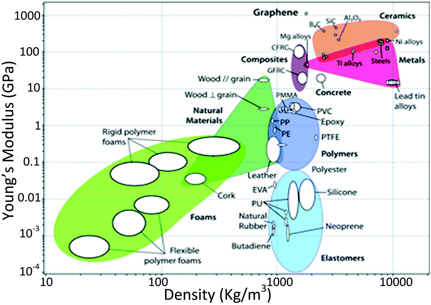 | ||
| Fig. 107 Chart of Young's modulus as a function of density comparing graphene properties to more traditional materials. Green ellipse, foams; cyan ellipse, elastomers; blue ellipse, polymers; olive triangle, natural materials; purple ellipse, composites; magenta triangle, metals; orange ellipse, ceramics. The white circles and ellipses are referring to a particular material inside each of the listed classes of materials. Note the axes are in logarithmic scale. Graphene density was taken as 2200 kg m−3.2085 PVC, Polyvinyl chloride, PTFE, Polytetrafluoroethylene; GFRC, glass fiber reinforced concrete; CFRC, ceramic fiber reinforced concrete. | ||
Graphene-based polymer nanocomposites and graphene–nanometals–polymer hybrids could provide improved mechanical properties and engineered electrical and thermal properties, fundamental for avionic/space and security applications.
In real applications, graphene layers could be used, even with properties that could be worse with respect to the ideal, defect-free, SLG. Indeed, charge and heat transport are perturbed at inter-sheet domain boundaries, edge defects act as electronic traps, and different sheets might split apart under mechanical stress, causing device malfunctioning or failure. Furthermore, while record properties can be obtained for isolated graphene, for real world applications graphene will have to be either deposited on or embedded in a third material, which will perturb, often significantly, its properties.
Here, we discuss some of the most promising applications of graphene in composites and 3d bulk materials, having different TRL. Some of the applications, such as graphene enhanced carbon fibre composites for structural reinforcement, are already commercialized in tennis rackets,2067 while others, such as applications for photonics,995,1058 still require more fundamental research.
11.1. Polymer-based composites
In order to exploit on a macroscopic scale some of the unique properties of graphene, one can integrate it as nanofiller dispersed in a polymer or inorganic matrix.Up to date, most efforts focused on polymer matrices, showing large increases in Young's modulus,2068 tensile strength,2069 and electrical703,2070 and thermal2071 conductivity, particularly at low volume fractions (<1%).703,2070 Inorganic matrices have received comparatively little attention, but the results so far show that the addition of graphene to ceramic matrices produces large increments in fracture toughness (Pa × m1/2) (235% increase at 1.5 vol%),2072σ (172 S m−1 at 2 wt%)2073 and EMI shielding (>99% attenuation for 30 wt%).2074 However, this field is still in its infancy and several challenges and open questions remain, such as improvement in composite properties at large volume fractions, integration into fibre-reinforced composites, determining scaling behaviour of mechanical and transport properties in nanocomposites, and how graphene–matrix interactions at the nanoscale are related to bulk composite properties.
The advantages of graphene over traditional fillers and other materials stems from its combination of mechanical and transport properties, as well as chemical and thermal resistance, high surface area and low thermal expansion coefficient. While some of these properties are shared by CNTs, its 2d shape, one-atom thickness and edge atoms provide an advantage in several applications, see Table 8. The large surface area implies that in a composite the graphene–matrix interface is also very large, thus becoming a powerful engineering parameter to tailor properties. In addition, the combination of size, SSA and κ of the nanofiller modifies the matrix properties at the interface by acting as a nucleation point and a heat sink which can stabilise new phases, affect pore structure and overall matrix properties.673,684,2075–2085 These effects deserve further study by modelling and experiments to better understand stress, charge and heat transfer at the graphene–matrix interface, targeting the development of the applications outlined above.
| Composite property improvement | Target application |
|---|---|
| Mechanical properties | Structural applications for sporting goods, aeronautics, aerospace, automotive, military (body armours, etc.) |
| Electrical conductivity (σ) | EMI, antistatics, electro-machining. |
| Thermal conductivity (κ) | Heat dissipation in Si-based electronic devices avoiding thermal mismatch. Metal replacement for heat exchangers where corrosion resistance and light weight are required. |
| Gas permeation | Gas barriers in packaging |
| Surface area | Catalysis |
An emerging area is the development of bioinspired composites, reinforced with macroscopic fibres (e.g. carbon fibre) and graphene, with the nanofiller at low volume fractions and dispersed in the matrix (where it is more efficient for increasing the toughness of the interface), adding functionality, as already demonstrated in the case of CNTs2086,2087 and related composites.2088 The interplay and synergy between material mixing and hierarchy was studied by theory and simulations.2089,2090 A graphene crumpled hierarchical multifunctional surface was realized;2091 the result was a tuneable, highly stretchable, conductive and superhydrophobic2092 (i.e. difficult to wet, where the contact angles of a water droplet exceeds 150°) electrode, ideal for next generation flexible electronics.
This bioinspired route could be a fast vehicle for the incorporation of graphene in a range of industrial applications (aerospace, automotive, etc.), thus deserves further studies by a combination of modelling and experiments, taking into account the whole life-cycle of the materials, addressing issues such as graphene effects on composite processing (e.g. sintering, extrusion), novel properties and recycling/reusing opportunities.
MD simulations were used to study the interfacial thermal resistance in graphene/polymer nanocomposites2093 and to compare the heat transfer properties of graphene and CNT polymer nanocomposites.2093 The interfacial mechanical behaviour of the graphene/polymer system was analysed by Consistent Valence Force Field (CVFF),2094i.e. parameterization of bond lengths and angles with quantum chemical ab initio methods, to describe the atomistic interactions.2095 However, the literature is still scarce and further studies are required.
A crucial step will be the dispersion of the carbon nanofillers. A well dispersed state ensures a maximized reinforced surface area, which will affect the neighbouring polymer chains and, consequently, the properties of the whole matrix, see Fig. 108 and Table 9.
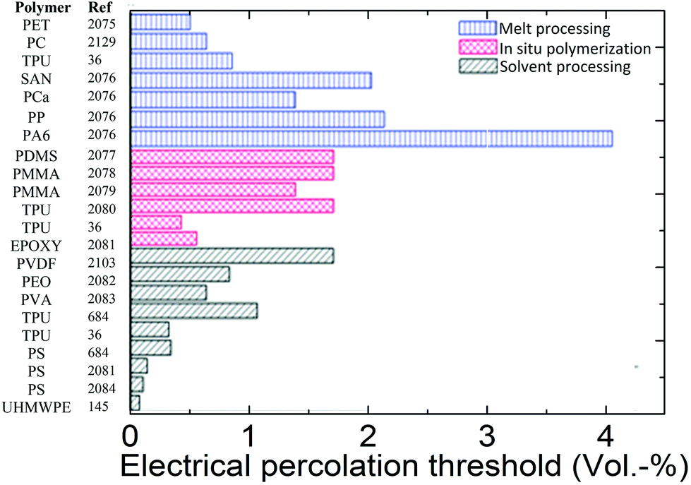 | ||
| Fig. 108 Electrical percolation data of graphene/polymer nanocomposites, produced with different processing approaches, e.g. melt processing (blue bars), in situ polymerization (red bars) and polymerization via solution processing (grey bars). | ||
| Polymer | Reinforcements | Graphene concentration (vol%) | Modulus increase (%) | Tensile strength increase (%) | Ultimate strain increase (%) | Ref. |
|---|---|---|---|---|---|---|
| PVA | GO | 2.5 | 128 | 70 | 32 | 2097 |
| PVA | GO | 0.49 | 62 | 76 | −70 | 2098 |
| PMMA | GO | 1.7 | 54 | N/A | N/A | 2099 |
| PCL | GO | 2.4 | 108 | 36 | −90 | 2100 |
| PCL | GO | 0.46 | 50 | N/A | N/A | 2101 |
| Epoxy | FG | 0.05) | 31 | 40 | N/A | 2129 |
| PEN | FG | 2.4 | 57 | N/A | N/A | 2102 |
| PCA | FG | 1.3 | 25 | N/A | N/A | 2103 |
| PMMA | FG | (0.005, 0.5) | 33, 80 | N/A | N/A | 36 |
| PVDF | FG | 3.1 | 92 | N/A | N/A | 2104 |
| SAN | FG | 2.3 | 34 | N/A | −58 | 2105 |
| Natural rubber | FG | 1.2 | 750 | N/A | N/A | 2106 |
| PDMS | FG | 2.2 | 1100 | N/A | N/A | 2106 |
| Styrene-butadiene rubber | FG | 0.8 | 390 | N/A | N/A | 2106 |
| TPU | FG | 1.5 | 43 | −23 | −15 | 2107 |
| Silicone foam | FG | 0.12 | 200 | N/A | N/A | 2108 |
| PVA | Acid functionalized graphene | 0.34 | 35 | N/A | N/A | 2109 |
| PMMA | Amine treated acid functionalized graphene | 0.3 | 70 | N/A | N/A | 2109 |
| TPU | FG | 1.6 | 250 | N/A | N/A | 2110 |
| 1.6 | 680 | N/A | N/A | |||
| 1.5 | 210 | N/A | N/A | |||
| GO | 1.6 | 490–900 | N/A | N/A | 2110 | |
| PS | PS-functionalized chemically reduced GO | 0.4 | 57 | N/A | N/A | 2111 |
| TPU | chemically reduced sulfonated-graphene | 0.5 | 120 | 75 | N/A | 2112 |
| TPU | GO | 2.4 | 900 | −19 | −60 | 2113 |
| PAN | Exfoliation alkali GIC | 2.1 | 100 | N/A | N/A | 2114 |
Therefore, large efforts were devoted2096 to achieving homogeneous and well-dispersed systems by developing either covalent or non-covalent functionalisation of the filler surface.
The initial aim is to increase the composite modulus and strength by factors 2–4 with respect to plastic, at low loading level, <1%, so that the filler provides reinforcement without degrading any other properties nor significantly increasing weight. Later, one might expect to produce higher volume fractions, higher performance composites, with mechanical properties exceeding those of structural materials, such as steel, at a fraction of the density. In addition, adding GRMs to plastics may reduce gas permeability. This is very important for the beverage industry. E.g., beer manufacturers want to move from glass bottles to PET. However the shelf life of beer in PET is ∼2 weeks (cf. 30 weeks in glass).198,199,2115 To increase this shelf life, both oxygen and CO2 permeability, need to be cut by a factor of ∼5.199 DLC has been successfully used for such applications.198,199,2116 The permeability of a given plastic could be reduced by more than a factor of 10 for <5 vol% loading of platelets with aspect ratio >1000.2117 Thus, graphene could allow one to reduce the mass of plastic per bottle, i.e. reduce wall thickness.
Epoxy resin is a thermosetting polymer (i.e. it cross-links and toughens with T) and is widely used in various industries, including coatings, adhesives, electrical insulators, and composites.2118 Epoxy has excellent mechanical and chemical properties, including good dielectric properties,2119 high dimensional stability (the ability of a material to hold its shape over a period of time and for varying amounts of applied temperature, moisture, pressure, or other stress),2120 hardness,2121 flexibility,2122 and excellent chemical resistance (the ability of a material to avoid the permeability of different ions or molecules).2123 However, epoxy burns easily,2124 so research has been carried out to obtain a fire retardant epoxy.2125,2126 One of the most efficient ways to reduce the heat release rate, slowing thermal degradation of the polymer matrix and inhibiting heat and flammable gas release, is to use carbon materials.2127 Graphene sheets hold potential as new nanofiller and may be preferred over other nanofillers (CNT, carbon nanofiber, graphite nanoplatelets, etc.) owing to its higher surface area, aspect ratio, tensile strength, κ and σ.2128
Blended GO with epoxy, with high κ2071 (1.91 W mK−1) with respect to thermally conductive epoxy (∼1 W mK−1), has been demonstrated.2076 Nanocomposites with 5 wt% GO have shown a 4-fold increment of κ compared to pristine epoxy.2076 A comparison of the mechanical reinforcement of graphene flakes, SWNTs and MWNTs on the epoxy matrix at a nanofiller content of 0.1 wt% was reported in ref. 2129 indicating that graphene flakes out-perform CNTs in terms of Young's modulus, tensile strength and fracture toughness of the resulting composite.
11.2. Ceramic-based composites
Ceramic materials have very valuable properties from the engineering point of view, such as refractoriness (i.e. retaining material strength at T > 600 °C), strength and hardness,2130,2131 but they have an important drawback, their low toughness,2130,2131 which often overcomes their potential benefits.2132 The usual approach to increase toughness is the inclusion of second phase materials that may act as reinforcing agents by producing extrinsic toughening effects.2130,2131 This is the case of fiber containing composites, or CNT-ceramic composites, which received great attention, owing to the improved mechanical properties.2133 An extra benefit of CNTs is that they render the ceramic composites electrically conductive,2134 which enables machining by more efficient methods, such as electro-discharge.2135 This benefits from the erosive effect of electrical discharges or sparks2135 (note that, usually, ceramic materials are costly to machine into complex shapes as consequence of their high hardness and low toughness2136,2137).The above advantages may be transferred to graphene/ceramic composites. Initial studies show significant toughening2129 and higher electrical conductivity.2138,2139 Graphene ceramic composites also have further advantages compared to their CNT counterparts, such as the lower cost and commercial availability of graphene (e.g. RGO), and less stringent processing conditions. The latter aspect is of particular relevance when the high T (usually >1400 °C)2140 required to obtain ceramic materials is considered. In this respect, graphene/ceramic composites may be fabricated using conventional heating methods (e.g. hot isostatic pressing, a process that compresses and sinters the parts of the composite simultaneously in a T range from ∼480 to ∼1230 °C (ref. 2141), which reduces the porosity of metals and increase the density of ceramics),2141 instead of electric field assisted sintering techniques, a must for CNT/ceramic composites.2134
Graphene/ceramic composites might find applications in friction and wear related fields, such as engines components, bearings and cutting tools for metal working operations. Preliminary data show improved response of these composites under sliding contact,2142 where exfoliated graphene sheets seem to act as a solid lubricant.2142 The possibility of precise micromachining of hard ceramic composites exploiting the advantage of electrical conduction makes easier the fabrication of MEMS for high T uses.2143
Significant issues to be resolved include the atomic level characterization of the ceramic/graphene interfaces using HRTEM and focused ion beam methods for micromanipulation and imaging of selected areas. In situ mechanical testing under mechanical stress, e.g. inside an electron microscope, will help to understand the complex mechanical response of these composites.
11.3. 2d organic and inorganic nanocomposites based on chemically modified graphene
The multiple functional groups and unique 2d morphology make GRM ideal templates for the construction of 2d nanocomposites with various organic/inorganic components (see, e.g., ref. 709, 2144, 2145, and Fig. 109). | ||
| Fig. 109 Examples of 2d nanocomposites based on GRMs. (a) Assembly steps for a TiO2/GO nanocomposite from SDS-modified graphene sheets. (b) SEM image of a rutile TiO2/GO nanocomposite. (c) Fabrication process for GO based mesoporous silica sheets through the hydrolysis of tetraethylorthosilicate (TEOS), with cationic surfactant cetyl trimethylammonium bromide (CTAB)-functionalized GO as the template. (d) Lithium insertion and extraction in GMR sheets, where graphene acts as mini-current collectors during discharge and charge processes, facilitating the rapid diffusion of electrons during cycling processes.2144 | ||
CMGs can be viewed as 2d polymers containing extended aromatic frameworks and multiple functional groups.673 These groups can be used for the covalent attachment of organic and inorganic NPs, including MNPs, metal oxide NPs and QDs. The performance of nanostructured, hierarchical materials can be improved by controlling the self-assembly of the molecules in highly ordered 3d crystals,2146 or attaching small molecules to 1d scaffolds, such as linear, long polymeric chains.2147 The use of a 2d scaffold, such as a graphene sheet, is expected to provide 2d substrates allowing molecules to be positioned over flat but highly flexible (and solution processable) sheets.2148 In addition, selective grafting on different parts of the 2d surface may be achieved by exploiting the hydroxyl, carboxylic, epoxide groups present on the basal sheets or the edge sides as anchoring groups,2145,2145 allowing to tune the functional properties of the final hybrids by changing substitution pathways, type of linker and spatial positioning on the sheet. GO as scaffold instead of synthetic polymers gives advantages, because it can be produced on large scale and at low cost, and can form sheets with sizes up to 100 μm, unlike polymeric scaffolds which are 1d with lengths <1 μm.2058
The length of the linker between organic dyes and the GO surface strongly affects the optical properties of the attached molecules and the degree of quenching of the fluorescent dyes,709,2148 see Fig. 110. The graphene (opto)electronic properties can be deeply influenced by the presence of the molecule, due to charge-transfer and doping effects,2149 see Fig. 110.
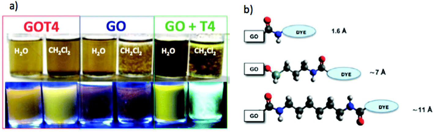 | ||
| Fig. 110 (a) Comparison of solubility and light emission of GO covalently linked to a fluorescent quater-thiophene molecule (GOT4), pure graphene oxide (GO), and a mixture of GO and the quater-thiophene molecule, with no covalent functionalization (GO + T4). For each case, the different solubility in polar (DMF–H2O, 1:5 in volume) and apolar (DMF–CH2Cl2, 1:5 in volume) solvent is shown, either in normal light (top) and under UV lamp (bottom). Adapted from ref. 709 (b) Linkers used in synthetic approaches to oligothiophene-modified GO.2058 | ||
By taking full advantage of synthetic chemistry, it is possible to create a new class of 2d shaped materials, where the sheets of graphene are used as a template, to create more complex and functional 2d sheets with organic or inorganic particles anchored to the graphene substrate.2058 The assembly of inorganic NPs on the surface of conductive GRMs not only avoids the agglomeration of NPs, but also increase the electrical conductivity.
To integrate their unique features, fabrication of 2d nanocomposites of GRMs and inorganic nanomaterials has been pursued.2144,2145 One of the most common strategies is to directly assemble GRMs with pre-prepared inorganic NPs. On the other hand, the in situ growth of inorganic NPs on the GRMs surface offers an alternative approach.
Various GRMs, including GO, RGO, modified GO/RGO and exfoliated graphene were explored for such purposes.2144 Several groups used graphene as template to grow NPs,2150 sheets2151 or ribbons2152 of iron oxide, sandwich-like titania nanosheets,2153 rutile and anatase TiO2 nanocrystals,2154 Mn3O4NPs,1882 and Ni(OH)2 nanoplatelets.1902
Ref. 2155 reported the single-step CVD synthesis of very thin MLGs on ZnO nano-structured networks. The material obtained in this way (termed aerographite2155) is completely black, despite its extremely low density (<200 μg cm−3). It is designed to be lightweight and at the same time robust to bear strong deformations.2155
Ref. 2156 obtained elastic, solid foams (pictured in Fig. 111) with a density lower than air by freeze-drying solutions of CNTs and large (∼18 μm) GO sheets. Ref. 2157 reported extremely elastic aerogels, which survive cyclic compression testing with strain up to 90%, from GO sheets by simultaneous functionalization and reduction of GO and assembly of RGO sheets into hydrogels with little stacking.
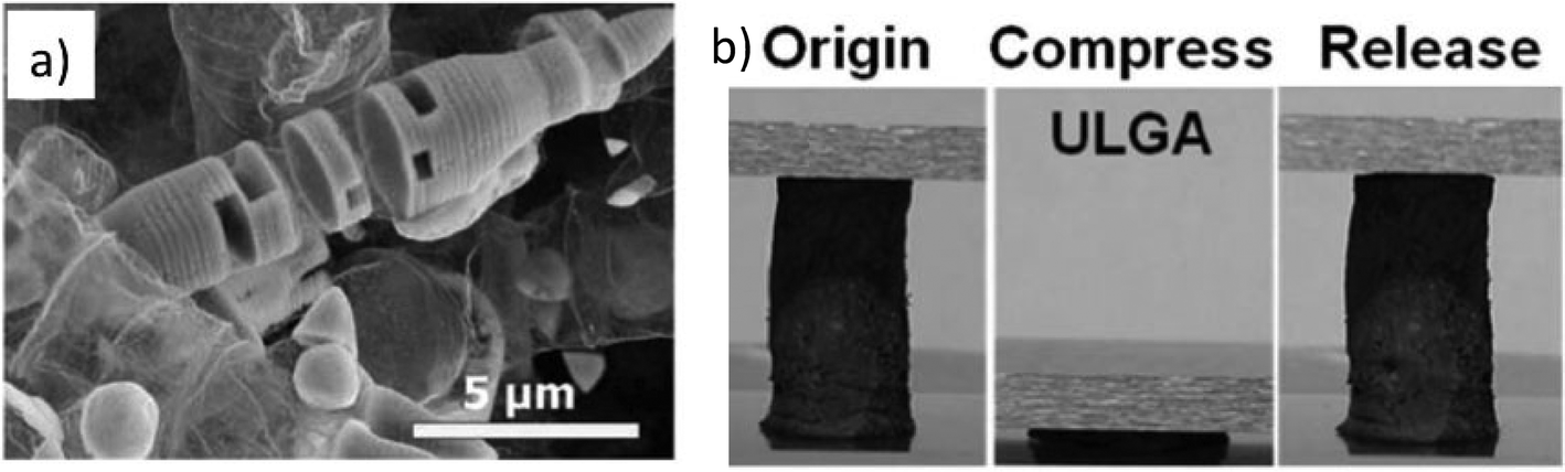 | ||
| Fig. 111 (a) Photograph of an intermediate state of a sample on its way from ZnO to Aerographite.2155 (b) Compressibility of GO based aerogel. ULGA is Ultralight and highly compressible Graphene Aerogels. Adapted from ref. 2157. | ||
Although similarly light carbon aerogels were made before,2158 they have relied on template scaffolds that were later etched away, a technique that limits the size of the final structure.2157 The resulting aerogels show density as low as 3 mg cm−3, yet the structure can fully recover without fracture even after 90% compression, suggesting applications in shock damping.2159
11.4. Photonic polymer composites
The demand in optical networking for photonic components that meet performance criteria as well as economic requirements opens the door to novel technologies capable of high-yield, low-cost manufacturing, while delivering high performance and enabling unique functions.2160 An optical communication system requires light sources and detectors, but many additional components make up modern transmission networks. Until the end of the 1980s, these components, including beam splitters, multiplexers and switches, consisted of bulk optics elements, such as lenses and prisms. Bulk optical components, however, are inconvenient to handle, highly sensitive to misalignment and prone to instability. All of these problems are avoided in integrated optics systems.2161 These combine miniaturised optical components and waveguides in a highly condensed chip-based device. Their compact, planar layout has clear advantages over bulk optics when deployed in complex systems. Integration permits the reduction of complex multi-function photonic circuits on a planar substrate.Polymeric materials are the ideal choice for such an integration platform.2160,2162,2163 They are easily manipulated by methods such as embossing, stamping, sawing, wet or dry etching. They have a low-cost, RT fabrication process. Polymers can be synthesized with customer defined optical characteristics, such as selective transparency bands in different spectral ranges, variable refractive indexes, low birefringence, other than high laser damage threshold and thermal stability. Moreover, the polymers must be easily processable during device fabrication and be economic.2164 Polymers traditionally used for optical applications include PMMA,2160 polycarbonate2165 and epoxy resins.2160
Deuterated2164 or halogenated polyacrylates2164 and fluorinated polyimides2160 were developed to address specific issues, such as optical losses,2166 heat2164 and environmental stability.2164 Water-soluble polymers, such as PVA,1353,2165,2167–2169 and cellulose derivatives, such as sodium carboxymethyl cellulose,1353,2170 have been widely used both for CNT and graphene-based SAs,1353,2171–2173 since stable, high-concentration dispersions can be readily prepared.1353 From the fabrication perspective, PVA is more attractive, because of its mechanical properties.1353 To prepare environmentally stable polymer composites, in particular, against humidity and T, graphene can be directly exfoliated in organic solvents.35 The dispersions are suitable for moisture resistant polymers, such as Polycarbonate and PMMA, or copolymers, such as SMMA.1353 Siloxane polymers have many attractive attributes, such as stable optical performance with low loss, making them viable for polymer waveguides. These can be spin-coated from uncured precursors or polymer solutions and then patterned into the specific waveguide geometries using either reactive ion etch or direct exposure to UV light patterns.
Precise control of the refractive index of both core and cladding material can optimise light transmission. Like inorganic materials,2174 polymers can be doped to take advantage of optical properties associated with the dopant.
Optical amplifiers are an important component in optical communications.2175 They are needed to enhance signals, particularly in order to compensate for the intrinsic losses due to fibre propagation and splitting, switching and multiplexing operations. Amplifiers can be housed in optical fibres or in integrated optics components. EDFAs2174 consist of an active region formed from a length of Er-doped silica fibre. They are often used in telecommunication networks to amplify optical signals in the 1310 and 1550 nm windows. With the emergence of polymer optical fibres,2176 the natural progression from silica-based EDFAs is the doping of rare earths into polymers.2177 There has also been increasing interest in doping rare earths in inorganic and organic waveguide components to make waveguide optical amplifiers.2178 The ease of integrated circuit fabrication provided by polymers, coupled with the expected high-gain performance in rare-earth polymer materials, lead to increased activity in this field.2179,2180
Many of the advantages of polymer materials discussed for communications systems also apply to lab-on-a-chip devices. The “lab-on-a-chip” combines a number of biological and chemical analysis processes into one miniaturized device.2181 Testing the optical behaviour is an important characterisation step, so integrated optics devices are often required in these new systems.2181 Lab-on-a-chip devices can be simplified by taking advantage of the ease of fabrication afforded by various polymer-patterning techniques.
A major technological challenge will be to develop of a new class of polymer-based optoelectronic devices embedding the optical and electronic functionalities of GRMs. These devices will combine the fabrication advantages of polymer photonics, with the tuneable active and passive optical properties of such materials. Such devices are expected to find a wide range of applications not only in optical communications, but also in bio-medical instruments, chemical analysis, time-resolved spectroscopy, electro-optical sampling, microscopy and surgery.
Novel photonic polymers incorporating GRMs need to be studied, e.g. index matching gels and optical adhesives. These are typically epoxy or silicone-based polymers, having excellent elastic and thermal properties, as well as good chemical stability. Current photonic polymers include acrylates,2160 polyimides1353,2160 polycarbonates1353,2160 and silicones.1353,2160 However, these give a significant optical loss (>0.5 dB cm−1) at the telecom wavelengths, due to C–O, O–H, Si–O and Si–H groups.2160 To achieve optimal 2d crystals-polymer devices, special formulations of silicone polymers need to be used. These could be fluorinated, to reduce the influence of Si–O and Si–H groups on the optical absorption in the telecom spectral window.2160 This could enable to set the optical losses at a very small value, less than 0.5 dB cm−1.
The timeline for the implementation of composites based on GRMs for different applications is shown in Fig. 112. Composites having different maturity are present, from those for structural applications, already at commercial level and produced in large scale, to graphene-based foams and composites with non graphene-2d materials, which might have interesting applications for flexible electronics and energy storage, but are still at the fundamental research level. The main targets are: 3 years: Functional composites for packaging; Hybrid composites. 3–7 years: Large scale production graphene nanoplatelets 7–10 years: GRMs functional composites for mechanical, photonic and energy applications.
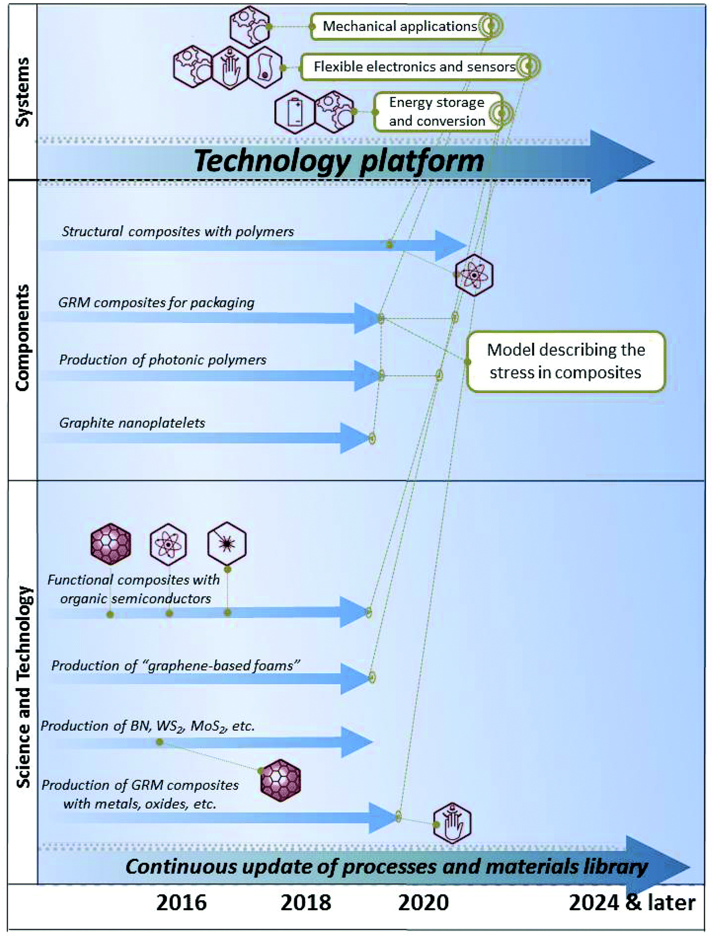 | ||
| Fig. 112 GRM-based composites development timeline. | ||
12. Biomedical applications
The application of nanotechnology for treatment, diagnosis, monitoring and control of biological systems is called “nanomedicine”.2182 NPs offer unique properties as drug delivery systems, and image agents.2183 They could also enable one to combine the diagnostic process with therapy (theranostics). Several NPs are available, ranging from polymeric and metallic ones, to liposomes, dendrimers, microcapsules, etc. All of these systems are currently under development.2184GRMs have recently attracted much attention for their potential use in nanomedicine and biology.2185 A common approach for covalent functionalization of graphene employs GO, which offers a new class of solution-dispersible polyaromatic platform for performing chemistry. The presence of the functional groups makes GO hydrophilic,703 allowing its dispersion in water.690 Moreover, the functional groups allow GO to interact with a wide range of inorganic and organic species in non-covalent, covalent and ionic manner, so that functional hybrids can be synthesized.2186 Furthermore, in contrast to pure graphene, GO is fluorescent over a broad range of wavelengths.689,2187 This tuneable fluorescence was used in biological applications for sensing2188,2189 and drug delivery.564 Additional chemical processing and modification should continue towards this end.
Research on graphene for biomedical applications is progressing quickly due to the previous know-how gained on CNTs,2190 since the surface chemistry is adaptable from one system to the other. Both materials show similar behaviour, with graphene providing additional functionalities with respect to CNTs, e.g. an enhanced loading of biomolecules, due to its 2d shape.2191
Current challenges include the controlled chemical functionalization of graphene with functional units to achieve both good processability in various media, and fine tuning of various physico-chemical properties. One aim of the controlled surface oxidation is the production of anchoring points for additional surface groups targeting: (1) attachment of biomolecules (peptides, DNA, growth factors…) via carboxyl groups: KOH/NaOH activation to induce carboxylic acid functional groups; (2) PEG coatings to get prolonged blood circulation half-life and avoid agglomeration; (3) Sulfonation; (4) Halogenation: fluorination changes the surface hydrophobicity, while surface bromination provides a starting point for conversion into other functional groups, such as amines, anilines, alcohols, or thiols.2192
GO provides a robust framework in which two or more components can be incorporated to give multifunctional capabilities.2193E.g., the conjugation of multiple components such as fluorescent molecules, tumour-targeting moieties, anticancer drugs or small interfering Ribonucleic acid (RNA) to GO represents a viable strategy not only to target human cancer, but also for imaging from inside the body by magnetic resonance or fluorescent imaging. The ability to simultaneously image and treat tumours with nanocarriers may provide advantages over conventional chemotherapies with the added value of reducing secondary effects. Nanocarriers are considered as molecular transporters to shuttle various types of biological molecules, including drugs, proteins, DNA, RNA, into cells by endocytosis.
All materials intended to be used in nanomedicine must be carefully tested and their potential effects on cells, animals and environment investigated.
The small size and the tuneable surface chemistry of graphene flakes allows them to efficiently interact with cells, be injected and diffuse further into tissues and into and through individual cells. Thus, in this respect, particle size is a key parameter. Indeed, size and shape control particle flow and cell internalization.2194 Graphene sheets may flow along capillaries, lymphatics or tumour vessels without obstructions. Flow will also be dependent on surface functionalization; aggregation of flakes should be avoided at any time.
For imaging agents it is essential to have a rapid clearance from blood to obtain low background signals and high quality images.2195 NPs surface charge and hydrodynamic diameter in presence of plasma proteins are important for their bio-distribution, excretion and rapid clearance from blood.2195
Size control and/or size separation of various scales is necessary to interface with biological systems in vitro or in vivo. Ultracentrifugation and filtering are the common ways to control size.35,250,642
Graphene has also potential in applications related to biosensing and bioelectronics. In particular, μ, together with chemical stability and low electronic noise,2196 offer an excellent platform for the development of FET-based biosensors.2197 Whereas μ has a direct influence on the device sensitivity by controlling the intrinsic transistor amplification,2196 the low noise observed in GFETs (down to 10 μV rms)2196 enables the detection of small electrical and chemical signals. The modification of the transistor's active area with functional groups and biomolecules (DNA, enzymes, antibodies, etc.) might allow for the development of sensors specific to particular analytes, which can find use in applications related to drug screening, proteomics, and genomics.
GFETs have also attracted attention for their potential use in bioelectronics, in particular for interfacing living cells and nerve tissue.2198 Further, the combination of excellent electronic properties, chemical stability, biocompatibility, and facile integration with flexible technology, makes graphene a candidate material platform for the next generation of neuroprostheses, i.e. devices that can substitute a motor, sensory or cognitive modality that might have been damaged as a result of an injury or a disease.
12.1. Imaging and diagnosis
Luminescent QDs are widely used for bio-labelling2199 and bio-imaging.2200 However, their toxicity2201 and potential environmental hazard2202 have limited their widespread use and in vivo applications. Fluorescent bio-compatible carbon-based nanomaterials might be a more suitable alternative. Fluorescent species in the IR and NIR are useful for biological applications, because cells and tissues show little auto-fluorescence in this region.2203 The optical properties could be exploited in biological and medical research, such as imaging, and, consequently, diagnosis.Luminescent graphene-based materials can now be routinely produced covering IR, visible and blue.328,689,2187,2204Ref. 564 exploited photoluminescent GO for live cell imaging in the NIR with little background.
The development of GRMs in this field needs to parallel the investigation of toxicity effects of these materials, as discussed in section 3.
12.2. Hyperthermia: photothermal ablation of tumours
Long and branched PEG coated CNTs and graphene exhibit prolonged blood circulation half-life.2205 This allows them to repeatedly pass through tumour vascularisation, with tumour uptake via the enhanced permeability and retention effect (EPRE)2206 of cancerous tumours. LPE graphene, due to its 2d nature and the achievable 10–50 nm dimensions,250 shows a better performance and distinctive behaviour with respect to CNTs, such as RES accumulation574 and improved EPRE,2207 promoting tumour passive targeting. This therapy is based on the energy transfer process occurring during the irradiation of a material generating heat sufficient for cell destruction at T > 40 °C.2208 Both CNTs and graphene are promising photothermal agents for in vivo tumour destruction.2209The hyperthermia treatment, where body tissues are exposed to slightly higher T than body T to damage and kill cancer cells, has the advantage of being less risky than surgery, chemotherapy and radiation therapy, due to fewer side effects and the possibility of repeat treatment. Hyperthermia is considered a promising alternative to conventional thermal ablation.2210 A broad variety of NPs with specific electrical, optical, and thermal properties was tested to induce enhanced hyperthermia,2210 with the aim to improve the treatment efficiency of conventional heating.2210
Ref. 2212 reported that encapsulated iron oxide NPs in a graphene matrix improve the electrical, optical, and thermal properties connected to hyperthermia applications. Also, graphene decorated with V/Au or Pt NPs improve the NP catalytic properties. Hydroxyapatite NPs have been grown on graphene2213 and are promising as scaffolds, according to “in vivo” experiments,2213 suggesting potential for in vivo nano-hyperthermia and cancer treatment.
12.3. Targeted drug delivery
Delivering medicines, see Fig. 113, to a patient in a controlled manner is one of the main research areas in nanomedicine.2182 The nanodevices carrying the medicines should deliver a certain amount of a therapeutic agent for a controlled period of time to a targeted diseased area within the body.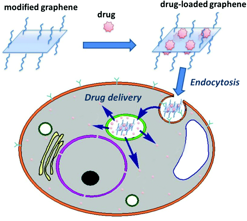 | ||
| Fig. 113 Scheme of drug delivery. Functionalized graphene loaded with the drug is internalized via endocytosis. The drug then escapes from the endosome and is released into the cytoplasm. Adapted from ref. 2211. | ||
Graphene's water soluble derivatives have potential application in drug delivery563,2214 and enzyme immobilization.2215 PEG-GO was applied as a nanocarrier to load anticancer drugs via non-covalent physisorption.2198 The loading and release of doxorubicin hydrochloride, e.g., was investigated as anticancer treatment.2198 The loading ratio (weight ratio of loaded drug with respect to carriers) of GO was up to 200% higher than with others nanocarriers, such as NPs, that usually have a loading ratio lower than 100%.2196 It was also reported that GO functionalized with sulfonic acid followed by covalent binding of folic acid allows to specifically target human breast cancer cells.2216 Controlled loading of two cancer drugs, such as doxorubicin2214 and camptothecin2217via π–π stacking and hydrophobic interactions was investigated.2216 These results pave the way to engineering graphene-based drug delivery.
12.4. Gene transfection
Genetic material (such as supercoiled DNA or small interfering ribonucleic acid – siRNA), or proteins, such as antibodies, may be transfected.2218–2220 This consists in intentionally introducing nucleic acids or other biological active molecules into the cells, changing the cell properties.2221 Gene therapy to cure diseases which are difficult for traditional clinical methods has been pursued for decades.2222 The major obstacle is to develop non-viral based safe and efficient gene delivery vehicles, in which nanomaterials are involved.2223–2226 Even though much progress has been reported on the use of cationic polymers and various nanomaterials, such as CNTs, silica NPs and nanodiamonds, as gene delivery vehicles,2223–2228 a lot more effort is still demanded to develop non-toxic nano-vectors with high gene transfection efficiency for potential gene therapy.GO bound with cationic polymers, such as polyethyleneimine (PEI), was used as nano-vehicle for gene transfection.2229 Cellular toxicity tests revealed that GO-PEI complexes exhibit significantly reduced toxicity to the treated cells compared to bare PEI.2229 Positively charged GO-PEI complexes are able to further bind with plasmid DNA (pDNA) for intracellular transfection of the enhanced green fluorescence protein (EGFP) gene in HeLa cells,2229 isolated for the first time from the cervical cancer2230 of Henrietta Laks (HeLa). While EGFP transfection with PEI appears to be ineffective,2229 high EGFP expression is observed using the corresponding GO-PEI as the transfection agent.2229 On the other hand, GO-PEI shows similar EGFP transfection effectiveness, but lower toxicity compared with PEI.2229 The first results2229 suggest graphene to be a novel gene delivery nano-vector with low cytotoxicity and high transfection efficiency, promising for applications in non-viral based gene therapy.
Whether and how the structure of graphene (e.g. size, thickness) would affect the gene transfection efficiency, however, remains an important question that requires further investigation. Small interfering ribonucleic acid with therapeutic functions may also be delivered by graphene complexes into cancer cells for potential gene therapy. This could be further combined with graphene-based chemotherapy and photothermal therapy, already demonstrated574,2214,2231 for the development of multimodal therapies of cancer.
12.5. Bioelectronics and biosensors
The integration of electronics with biological components is one of the current challenges on the path towards bioelectronics, which holds great promise for developing prostheses for ill or injured organs, as well as leading to a fundamental understanding of the brain.Biology and electronics may interface at three levels: molecular, cellular and skeletal. For any implanted bioelectronic material, the initial interactions at the bio-molecular level will determine long-term performance. While bioelectronic is frequently associated with skeletal level enhancements (e.g. artificial muscles), electronic communication with living cells is of interest for tissue engineering or for implants such as bionic eyes2232 or ears.2233
In the quest towards bioelectronics, different materials were proposed and investigated. The operation in physiological media demands special material properties,568 such as electrochemical stability, biocompatibility, and electronic and chemical functionality. Metals, Si and GaAs and carbon-based materials are expected to provide considerable advantages. Graphene offers a unique combination of physical, chemical and electronic properties, which may allow it to surpass the state-of-the-art for bioelectronics and biosensor applications.568,2234–2236 Indeed, graphene is impervious to the harsh ionic solutions found in the human body.2237 Moreover, graphene's ability to conduct electrical signals means it can interface with neurons and other cells that communicate by nerve impulse, or action potential.2237 These features make it promising for next-generation bionic technology.568,2237
Current research in nano-biosensors is experiencing a fast growth due to the wide range of novel applications for human healthcare. A biosensor combines a biological component with a physicochemical detector component and is designed for the detection of a certain analyte. Biosensors are used for sensitive and selective detection of biologically-relevant molecules, with applications in diagnosis (e.g. for the detection of cancer biomarkers), biomedical research, food quality control and environmental monitoring.2238
Since Si stability2239,2240 is rather low (i.e. Si oxidizes by interacting with atmospheric oxygen and organic solutions, or by hydrolysis with aqueous solutions, to give a SiO2 surface), the possible use of Si transistors in the human body requires coating with metal oxide (e.g. Ir oxide2241) to boost their stability.2237 Thus, other semiconductor technologies are also explored, such as GaN,2242 SiC2243 and diamond.2244–2246 There is however an ever increasing interest in flexible biosensors.2247 Another objective is to increase the device intelligence by integrating computation and decision power.
The use of graphene in biosensors may allow the development of flexible sensors, as well as improvement of impedance and biocompatibility, with a high added value. Graphene could also be used to implement grids of switches to control multi-array biosensors or integrate computing/decision power. The main applications are health, medical, pharmaceutical, impedance sensors, DNA chips, bio-labs on chip, bio-monitoring, and biomedical calibration.
This field requires transferable SLG or FLGs. Graphene on SiC could be also used, but is not appropriate if flexible devices are required. Good electrical properties, such as high μ and low electronic noise, are compulsory for applications in which very small signals are expected (below 100 μV), such as ultra-high sensitive biosensor991 or transistors for recording the electrical activity of nerve cells.2248 For less demanding applications, such as electrochemical detection of analytes for food and environmental monitoring,2249 the performance of other graphene materials (GO, graphene inks, etc.) might be sufficient.
The challenges for the development of ultra-sensitive graphene sensors on flexible substrates are many, but the impact of such technology could be even greater. Part of the technology challenges are similar to those shared by other applications of graphene. Amongst others, they include the preparation of high quality graphene films, novel concepts for surface nanostructuring using top-down semiconductor technology as well as nanopatterning with biomolecules based on (bottom-up) chemistry, etc. Other challenges are related to contact optimization (with a major impact on device performance) and passivation optimization (related to device stability). Further, novel functionalization and biofunctionalization methods have to be developed to control the selectivity of the graphene surface to different analytes. Such methods, which might be based on the modification of graphene, should not be detrimental for the electronic properties of this material.
One of the future targets is bidirectional communication (recording and stimulation) with neurons and nerve tissue, which should enable the study of how a neuronal network reacts and modifies itself. One goal of such research could be neural prostheses that augment or restore damaged or lost functions of the nervous system. The development of brain implants on flexible substrates, which can record the electrical and chemical activity of neurons, is fundamental for these applications. Primary adult retinal ganglion cells were shown to survive on CVD graphene even without any supporting glial layer (which serves as support cell for the neurons of the retina) or protein coating.2250 This, combined with the outstanding gate-sensitivity performance of solution-gated GFETs (exhibiting a transconductance two orders of magnitude larger than Si devices568) promises to surpass the state of the art technology for brain implants. Most current implants are based on metal electrodes.568 However, in addition to some issues with biocompatibility and stability under the harsh environment conditions of in vivo implants, metal electrodes do not offer the intrinsic FET amplification function.568 GFETs, on the other hand, can provide additional advantages due to the inherent amplification function of the FETs, such as an improved signal-to-noise ratio. Variations of the electrical and chemical environment in the vicinity of the FET gate region can be converted into a variation of the transistor current. Graphene can be employed to fabricate arrays of transistors568 to detect the electrical activity of electrogenic cells (i.e. electrically active cells, see Fig. 114), overcoming some of the limitations of the Si technology, such as the relatively high electric noise (typically, Si-based FETs exhibit an root mean square gate noise of few tens of microvolts, originating from trapping–detrapping processes at the Si/oxide interface2251) and the integration with flexible substrates. Moreover, Si-based materials are not stable under physiological conditions.2252,2253
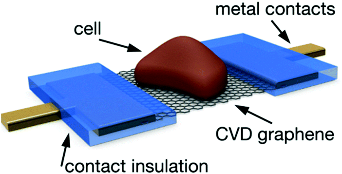 | ||
| Fig. 114 Schematic GFET with a cardiomyocyte cell (a cell of muscular tissue in the heart) on the gate area. The metal contacts (in brown) are insulated from the electrolyte by two layers of chemically stable and biocompatible SU8 photoresist (blue rectangles). [Adapted from ref. 568]. | ||
Other important challenges for bioelectronics and biosensor applications are the fabrication and in electrolyte characterization of graphene-based nanoelectrode arrays, the understanding of fundamental physical (and chemical) parameters, such as the impact of the Debye screening in reaching an ultimate precision in detecting the dynamics of chemical and biological systems, defining a proper biointerface that would be compatible with graphene and with a biological environment, extensive electrophysiology characterization of the electrical and chemical graphene/cell synapse, etc.
Future targets are the development of graphene-based bioelectronics and biosensor devices on a flexible substrates, such as parylene and kapton, already used for in vivo implants.568 Such graphene-based flexible devices might be exploited for the development of brain implants.2237 Moreover, studies could be conducted towards the realization of an artificial retina based on flexible GFET array, see Fig. 115.
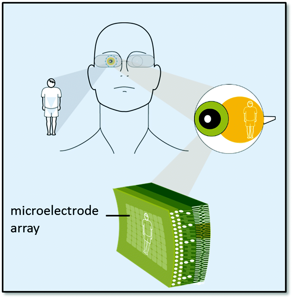 | ||
| Fig. 115 Concept for an artificial retina based on a flexible GFET array.2197 | ||
Degenerative retinal diseases, like retinitis pigmentosa and age-related macular degeneration, are amongst the most common origins of blindness.2254,2255 Electronic visual prostheses are a prospective therapeutic option of increasing importance in otherwise incurably impaired patients.2255 Several devices were tested in animal experiments and, according to the placement of the electrodes, possible stimulation sites are located subretinally,2256 epiretinally,2257 along the optic nerve,2255 or cortically.2255 The idea is to implant electrode arrays in the retina to inject current to the still-functional neural cells. Electrical patterns corresponding to visual images can then be created, and the brain can interpret them as vision.2254,2255 Anatomical, physiological and pathophysiological aspects must be considered.2254,2255 The optimal integration of the prosthesis into the highly complex system of the visual pathway is fundamental to provide an appropriate retinal substitute. In this context, a major challenge needs to be overcome: how to build implants which adapt to the eye's curvature.2258 This is necessary to prevent unwanted cell growth beneath the implant, other than being critical for good focus. Also, curved implants provide larger areas which can in turn capture larger images.2259
Because graphene is so thin, it could improve the interface between retinal implants and eye tissues. Graphene could be an ideal platform to tackle many other technical challenges. More efficient wireless data and energy supply, combined with decreasing space requirements, longer durability and increased safety are required.2255 Moreover, for high resolution, extremely small and densely mounted electrodes are needed. From today's perspective it is unclear in which approach graphene will lead to the best functional long-term results. However, it may be assumed that there will not be one single universal solution and the specific adjustment of a method to a particular disease will be fundamental.2255
12.6. Thin films, joint prostheses
Some medical applications require hydrophobic materials with a non-cell adhesive surface, such as devices in contact with human blood (e.g. artificial heart valves) or joint prostheses in the friction area, while others need a cell-adhesive surface to assure complete tissue integration of the implanted material in the human body. Graphene may be another possibility as biocompatible coating together with other carbon layers, such as nano-diamond coatings2260 or DLC.2261 For this purpose, graphene-inks deposition techniques, as well as growth on metals, should adapt to have a competitive cost and be able to cover large and complexes surfaces. Graphene could be useful as coating of medical tools. However, this research area is still at the beginning, with huge improvement needed.2262,2263Graphene might also be used as reinforcement for polymeric and ceramic prostheses. Small percentages of graphene or GO improve polymer elongation at break,2264 leading to tougher materials.2264 These graphene-based polymer composites can also exhibit good tribological properties,2264 the starting point towards the realization of prostheses.2264
12.7. Single-molecule genomic screening devices
The translocation of proteins and DNA through nanopores is becoming a key tool for the detection of single molecules.2265,2266 Nanopores – nanosized holes that can transport ions and molecules – are very promising for genomic screening, in particular DNA sequencing,2267 by rapid electronic detection of the base sequence of single DNA molecules. DNA sequencing is rapidly growing into an industry of major interest. A variety of ‘conventional’ techniques exist, each with their own pros and cons.2268 The idea of using nanopores for DNA sequencing was proposed over 20 years ago.2269 The first experimental proof of translocation of DNA molecules was reported in 1996 using the biological protein pore α-hemolysin,2270 albeit without sequence information. It has taken significantly more time to establish that single nucleotides can be discriminated within the traversing DNA, most prominently because the speed of translocating DNA has been too fast (∼μs per base) to identify individual bases.2271 In theory, the basic idea of nanopores sequencing is straightforward: pass a DNA molecule from head to tail through a nanoscale pore in a membrane, and read off each base when it is located at the narrowest constriction of the pore, using the ion current passing through the pore to probe the identity of the base.Single-stranded DNA molecules were statically captured in a α-hemolysin nanopore using a DNA hairpin (unpaired loop in a single-stranded DNA – ssDNA)2273 or a protein attached to the DNA end, either of which are too large to enter the pore. This allowed the detection of single-nucleotide mutations in the immobilized DNA.2274–2276Ref. 2277 modified α-hemolysin to include a cyclodextrin ring that binds free mononucleotides, which therefore reside in the pore for long enough (up to 10 ms) to be distinguished by ionic current levels for each of the four bases.2277
More recently, the use of DNA polymerases (enzymes that synthesise DNA) that drive a DNA template through a nanopore in single-nucleotide steps as DNA is synthesized was suggested.2278Ref. 2278 found that certain DNA polymerases were potentially suitable to this approach because they remained bound to DNA, even against the force of an applied voltage needed to insert the DNA into the pore. The polymerase, which processes DNA at a rate of about one nucleotide every 10 ms or slower,982 lowered the translocation speed of DNA by four orders of magnitude compared to freely translocating DNA.2278
Other advantages of nanopore sequencing with respect to other techniques include the single-molecule read-out, the fact that multiple molecules can be processed by a single pore, the absence of expensive fluorophore labelling, and the lack of amplification steps.
Looking ahead, a number of improvements are needed. The error rate must be decreased (a 4% error rate was reported in ref. 2279), the read length needs to be increased further, and the stability of the protein pores over time needs improvement. Current state of the art solid-state nanopores suffer the drawback that the channel is long, ∼100 times the distance between two bases in a DNA molecule (0.5 nm for ss DNA). E.g., conventional Si-based nanopore membranes are ∼30 nm thick,982 corresponding to ∼60 bases along a ssDNA molecule. They are therefore not directly useful as-is in DNA sequencing applications, although solid-state nanopores are excellent new tools for biophysical studies.2268
Suspended graphene membranes are ideal for this new class of sensors, as they are atomically thin, stable, inert, and can be patterned with atomic resolution,317,2272Fig. 116(a).
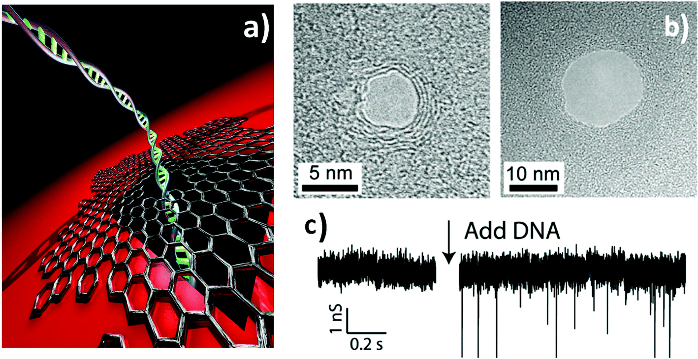 | ||
| Fig. 116 Nanopore sensors for detecting the translocation of single DNA molecules. (a) Illustration of DNA molecule passing through a nanopore in a suspended SLG. (b) Transmission electron micrograph of a nanopore drilled using an electron beam in (left) MLG and (right) SLG. (c) Conductance as a function of time (left) before and (right) during translocation of double-stranded DNA across a 22 nm graphene nanopore. The spikes indicate blockage events. Adapted from ref. 980. | ||
Ref. 980, 2280 demonstrated that ultrathin nanopores fabricated in SLG can be exploited to realize single-molecule DNA translocation. A small nano-size hole can be drilled into a graphene membrane by direct knock-on damage, Fig. 116(b), using the focused electron beam of a TEM,2280,2281 or alternatively by a focused ion beam.2282,2283 This membrane is subsequently placed between two reservoirs of liquid, and a ionic current can then be measured across the membrane. The traversal of single DNA molecules through the hole can be monitored as temporal changes in the ionic current,980Fig. 116(c). As individual DNA molecules translocate through the pore and DNA blocks the path for ionic current, characteristic temporary conductance changes are observed in the ionic current through the nanopore, allowing single molecule detection, and setting the stage for future single-molecule genomic screening devices.980
Ref. 334 formed 12 nm gaps between two graphene electrodes, which act as electrical contacts for molecules that bridge the gap, see Fig. 117. The devices are stable at RT. This technique could be used to contact a variety of objects (molecules, particles), as well as to explore functionalization of the contacts. The graphene electrodes in turn may be contacted by a variety of metals, including ferromagnets, superconductors, etc. Building on the early experiments on DNA translocation,980,2280 sensitivity can be pushed with the ultimate goal of resolving individual bases in ssDNA. As an alternative to measuring ionic currents, devices may be developed based on the control of tunnelling current between two sheets of graphene by the passage of a DNA molecule.
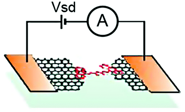 | ||
| Fig. 117 Single-molecule transistor with graphene electrodes [Adapted form ref. 334]. | ||
With further optimization of the patterning, i.e. smaller and more consistently shaped holes, the precision and spatial resolution of the process may be further increased. Mild oxidation2284 and carbothermal etching2285 processes, sensitive to the crystal orientation, could be employed to improve the regularity of such holes. In concert with corresponding progress in readout circuitry, as well as modelling, this could lead to consistent discrimination between individual base-pairs, therefore, in turn, sequencing of DNA molecules. A key challenge is how to progress towards practical fabrication of such sensors, as patterning using TEM or focused ion beams is slow and inconvenient compared to the requirements of large-scale fabrication.
Modelling and data analysis should improve in order to correctly interpret signals from DNA molecules passing through larger holes (e.g. 10 nm diameters). Ultrahigh resolution patterning strategies with potential for upscaling should be developed, possibly bottom-up, like BC lithography,331 nanosphere lithography1706 or other types of self-assembled etch masks. Most of these methods, however, are much better suited for making large arrays of patterns than individual nanopores. While proof-of-concept DNA sequencing is a prime target, the long-term success of such a technology requires substantial efforts in developing atomic-precision nanopatterning with higher throughput.
12.8. Plasmonic biosensors
SPR biosensors2290 are currently the most widely used platform for label-free, real time sensing and monitoring of biomolecules and molecular reaction events.2290 We can typically distinguish two classes: (a) Prism-coupled SPR sensors,2291 utilizing propagating SPP on a flat functionalized thin metal film. SPPs are excited at specific angles and wavelengths resulting into a sharp dip in reflectance (see Fig. 118a). Sensing occurs by monitoring the change in resonant angle or wavelength caused by adsorbed analytes on the metal surface.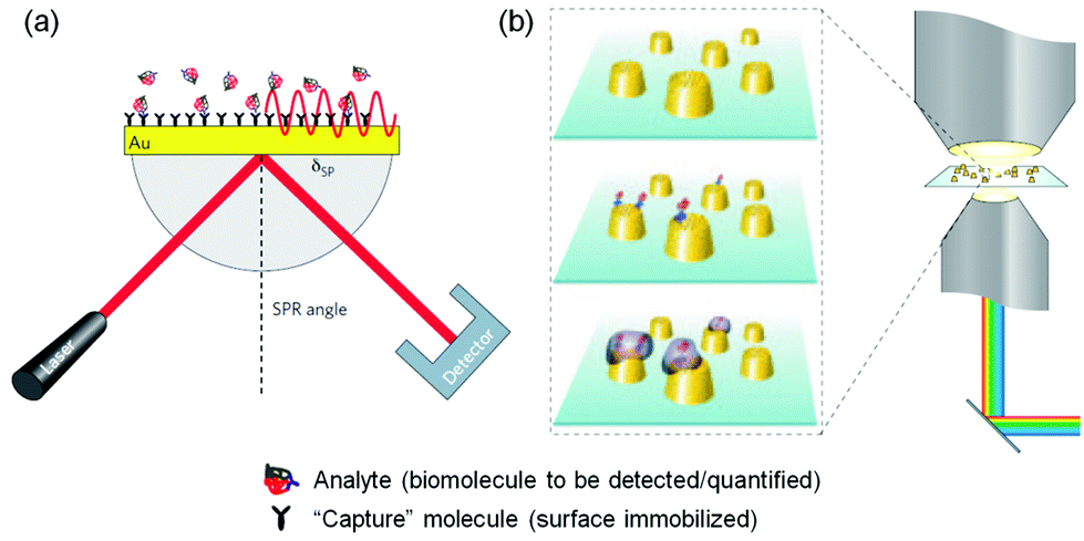 | ||
| Fig. 118 (a) Scheme of a prism-coupled SPR biosensor in the Kretschmann configuration (where a thin metallic layer is formed on the substrate and acts itself as the spacer).2286 A high-index prism is used to match the incident wave's wavevector lateral component to the SPP wavevector.2287,2288 (b) Scheme of a nanoplasmonic biosensor. Functionalized nanoparticles can be simultaneously interrogated within an optical imaging approach. Adapted from ref. 2290, 2289. | ||
This is the commercial standard providing the best sensitivity and proven functionality, at the expense, however, of necessitating bulky optical components and alignment systems, prohibiting compact, low-cost devices, and high-throughput bioanalytical measurements.
Recent proposals to overcome this limitation2292,2293 include SPP excitation by nanoholes,2290,2294 nanopits,2295 nanoslits2296 or gratings,2297 with the possibility of utilizing SPP interference in a Mach–Zehnder (MZ) interferometric configuration.2298–2300 (b) Nanoplasmonic sensors,2301–2303 utilizing localized SPR (LSPRs) in NP assemblies,2304–2306 and metamaterials,2307,2308 typically excited by normally-incident collimated beams. The plasmonic nanostructures exhibit sharp resonances due to LSPRs, and sensing occurs by monitoring the change in resonance wavelength caused by analytes adsorbed on the nanostructured metal surface (see Fig. 118b). This configuration enables an imaging scheme for a low-cost, miniaturized, high-throughput on-chip biosensing platform. With careful tuning and optimization of the metal nanostructures, nanoplasmonic sensors can surpass the performance levels of state of the art commercial prism-coupled SPR sensors,2309 offer single molecule detection2305,2306 with label-free biosensing methods.2310
Graphene has several properties that could enhance biosensing: intrinsic plasmons in the IR to THz range with high field concentration252,1321,1326 and long life-time,1321,1579,1580 constant absorption in visible to IR,990 high biomolecule functionalization capability due to π-stacking interactions,2311–2313 low small molecule permeability offering passivation against corrosion.2062,2314,2315 In particular, graphene can provide new perspectives in plasmonic sensing in three main ways: (1) as a functional surface, which supports intrinsic surface plasmons at IR frequencies: SPPs in bulk and LSPRs in nanostructured graphene, (2) as a functional gate-tuneable coating for existing plasmonic devices: functionalization of Au and Ag surfaces (bulk or nanostructured), LSPR control and tuning via gating, protection against corrosion for Ag and Cu2339 (3) as a direct transducer eliminating the need for optical detection.
The vision for graphene-based plasmonic sensing in 10 years and beyond is the development of a low-cost, ultra-sensitive, ultra-compact, label-free, on-chip, high-throughput and realtime sensing platform.
Utilizing the intrinsic plasmons of graphene for biosensing has not yet been demonstrated. Theoretically, a high-index prism coupling system to match the incident wave's wavevector lateral component to the SPP wavevector, either in Kretschmann geometry (prism in contact with graphene, see Fig. 118a)2287,2288 or Otto geometry (prism at subwavelength separation from graphene and coupling via attenuated total reflection),2309,2316 could be adequate in exciting THz SPPs in highly-doped SLG or FLG.2317 Additionally, graphene LSPRs can be used either in an index sensing setup,2318i.e. measuring the reflection or transmission spectrum shift when biomolecule binding events that change the local environment occur on their surface or, in a surface-enhanced infrared absorption (based on the enhancement of the IR absorption of organic molecules in proximity of noble metal substrates) (SEIRA2319–2321) setup, where the LSPR is tuned to the analyte's molecular vibration modes and serves as a substrate for enhanced absorption.2318 For SEIRA, the possibility of dynamic tuning the LSPR frequency may enable simultaneous multimode detection. Finally, SPPs excited on GNR waveguides and waveguide pairs1325 could be used in a MZ interferometric setup.
A performance improvement factor of (1 + 0.0025Nψ) was estimated,2322 where ψ > 1 is the ratio of the number of biomolecules adsorbed on the graphene/Au surface to those adsorbed on a bare Au surface. Graphene was also shown to significantly modify the LSPR of Au nanorods when placed on top of them,2323 making their optical response particularly sensitive to charge transfer events,2323 theoretically down to single charge transfer events.2323 SPPs on Ag films and LSPRs on nanostructured Ag exhibit a sharper response curve and can thus offer superior sensitivity compared to Au.2324 The main problem of Ag as a sensing platform is its low resistance to sulfidation (introduction of sulfide ions in a material),2325,2326 detrimental to the plasmonic response.2326 Graphene's impermeability to small molecules is a viable solution for Ag surface passivation2327 (see Fig. 119a), which, when combined with graphene's ease of functionalization, may enable Ag-based biosensing.2328,2339 At the same time, graphene-protected Cu survives in air and water environments, provides much better phase sensitivities for SPR detection compared to Au, sustains nano-fabrications and opens a field of graphene-protected Cu-based plasmonics.2339
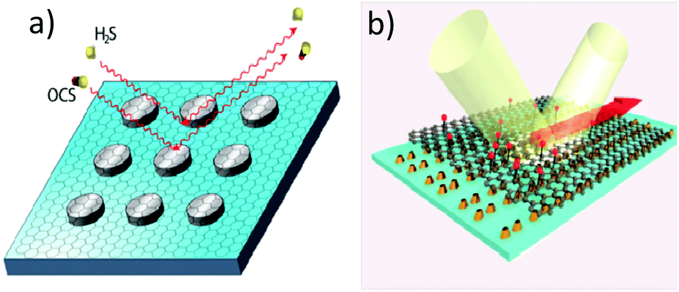 | ||
| Fig. 119 (a) Illustration of graphene-passivated Ag nanoantennas fabricated in a square array. The graphene layer prevents the reaction of trace atmospheric hydrogen sulfide (H2S) and carbonyl sulfide (OCS) with the Ag surface. Adapted from ref. 2327. (b) Scheme of a square array of Au double-dots on a glass substrate covered by hydrogenated graphene. Adapted from ref. 2310. | ||
Metamaterials based on subwavelength MNP assemblies can be tuned to provide narrow optical resonances,2329–2331 important for increased sensitivity. Graphene on top of a metamaterial works as a functionalization layer, allowing the adsorption of biomolecules close to the metamaterial surface. Such a scheme was demonstrated with split-ring resonators2332 and diffractively coupled NP arrangements that yield topologically protected zero reflection [i.e. the metamaterial's effective index as a function of frequency crosses the zero-reflection line on the complex index (n, k) plane, whereby there is always a frequency at which zero-reflection is obtained irrespective of structure imperfections or variations] accompanied by phase sensitivity, measured through an ellipsometric setup2310 (see Fig. 119b). In the latter case, the sensitivity can be better than 1 fg mm−2 (ref. 2310), over 3 orders of magnitude better than state-of-the-art SPR sensors,2291 and within the realm of labelling methods, making this the ultimate SPR-biosensor platform.
 | ||
| Fig. 120 (a) Schematic plasmonic MZ interferometer. Adapted from ref. 2299. (b) Schematic plasmonic interferometer using grating coupling and an integrated graphene transducer. | ||
After excitation, the SPPs propagate towards another slit where they interfere. Dielectric environment changes cause phase differences between the two interfering SPP waves, which are recorded in the far field radiation.2299,2300 Refractive index sensitivities of 3500 nm RIU−1 (i.e. SPP wavelength shift per refractive index unit change), just 4 times lower than commercial prism-based SPR sensors, have been reported.2291 In all cases the interference is optically monitored through a microscope objective.
Besides its use as a passivation and functionalization coating on one of the MZ arms, graphene can find novel functionality as a direct transducer. Ref. 2333 proposed a scheme similar to graphene-based PDs,446,1433 which eliminates the need for optical detection and enables an ultra-compact integratable sensing platform. Graphene-based transduction of optical signal for biodetection was reported with a dielectric waveguide sensing scheme.2334
Ref. 2333 proposed a grating for SPP excitation, after which the plasmons propagate towards a graphene-covered slit where they independently interfere with the incoming wave.
The two MZ arm lengths are asymmetric to enable a net photovoltage response, and fine-tuned for maximal sensitivity. Further extensions to this scheme include graphene for functionalizing one or both of the sensor arms, and a MZ scheme that removes the need of the metal and utilizes intrinsic IR plasmons in graphene ribbon waveguides.
Fig. 121 shows the timeline for biosensing and biomedical applications.
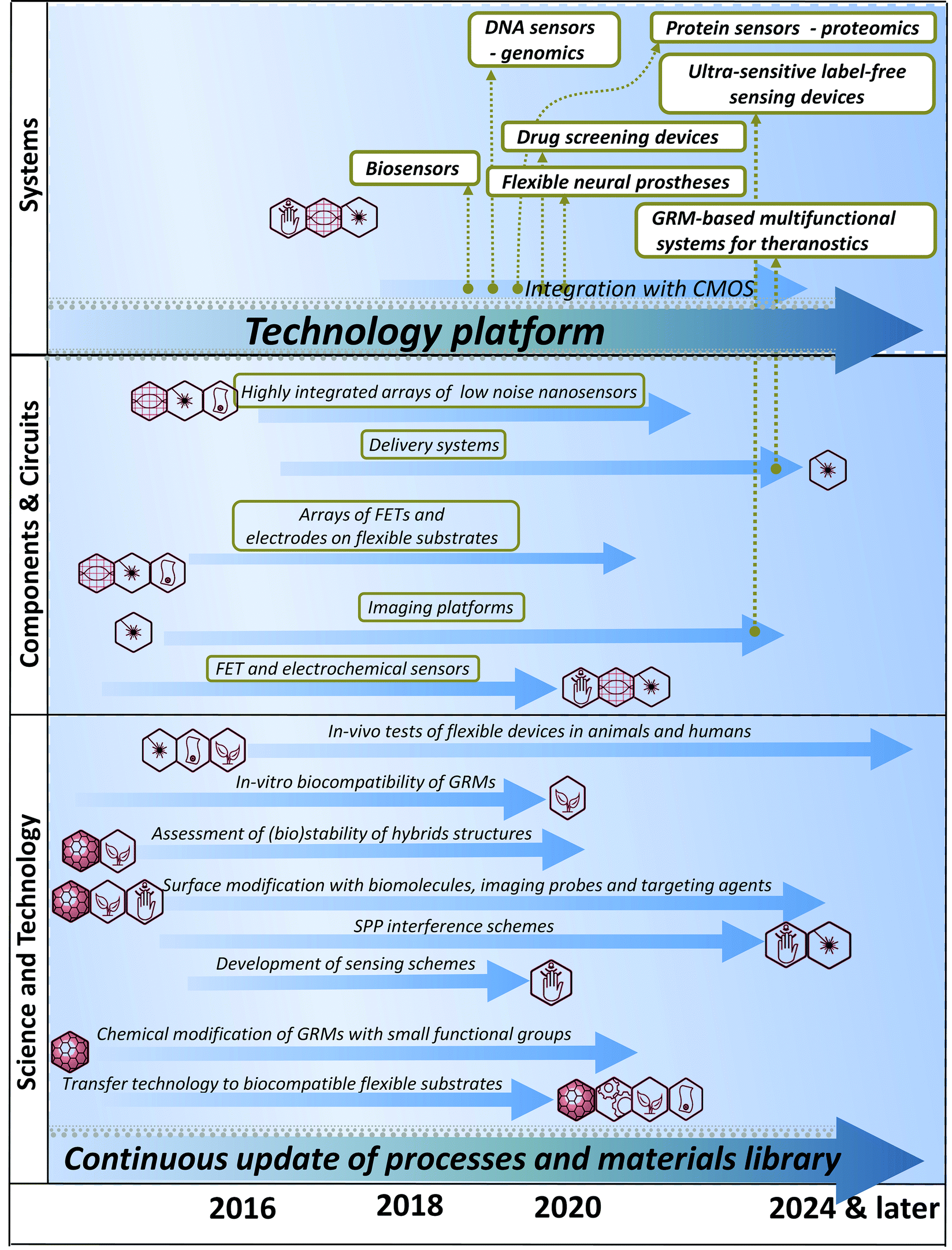 | ||
| Fig. 121 Biomedical applications timeline. | ||
13. Conclusions
The field of graphene, related 2d crystals and hybrids is now rapidly evolving from pure science to technology. Different applications require GRMs with diverse properties, from structurally perfect and high μ graphene for high tech electronics, to defective materials for energy applications, e.g. batteries and supercapacitors.The current and near future market for GRM applications is driven by the production strategies for these materials. Once each production route is mature enough, this will enable a widespread practical implementation of these materials. Thus, as summarized in the detailed roadmaps in Fig. 122, the availability of a product for the end user is strictly dependent on the different pace of the material development. The cheapest GRMs and with the least stringent requirements could be the first available on the market, to be used, e.g., in flexible electronic devices based on conductive inks, such as flexible solar cells, batteries and supercapacitors, while devices which require the highest, electronic quality grade, such as spin valves, non-volatile memories, will take more time to progress.
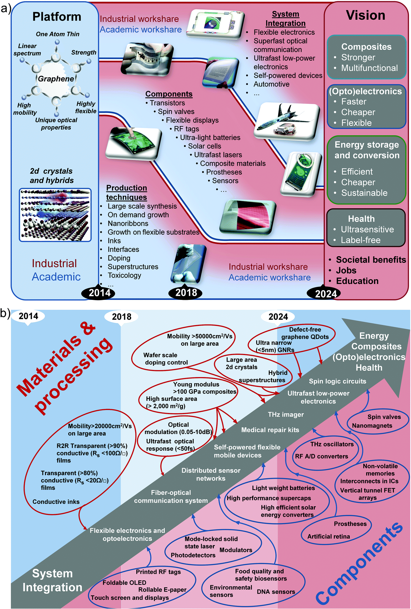 | ||
| Fig. 122 The STRs follow a hierarchical structure where the strategic level in a) is connected to the more detailed roadmap shown in b). These general roadmaps are the condensed form of the topical roadmaps presented in the previous sections, and give technological targets for key applications to become commercially competitive and the forecasts for when the targets are predicted to be met. | ||
The target is to develop novel applications, planned thanks to each GRM unique properties, rather than try to replace other materials in existing applications. GRMs will replace existing standard materials only if the properties of the new components are amply competitive to justify the cost for changing current industrial processes.
Acknowledgements
We acknowledge useful discussions with A. K. Geim, K. von Klitzing, S. Haque, C. Kerr, R. Phaal, N. Athanassopoulou, R. S. Ruoff, G. Yu, M. Stoller, P. Avouris, C. W. J. Beenakker, V. Amendola, M. Meneghetti, L. J. Biró, E. Burovski, G. Calogero, C. P. Grey, M. Lemme, D. Chang, V. Cheianov, Luciano Colombo, M. Dragoman, N. Drummond, R. Dryfe, M. Fogelström, J-C. Gabriel, P. G. Gucciardi, M. G. Donato, C. S. Vasi, P. H. Jones, R. Saija, S. Savasta, T. Hasan, A. Isacsson, M. Inguscio, J. Iwaszkiewicz, U. Jansson, L. Jansen, A.-P. Jauho, V. Raineri, D. Jimenez, S. Kubatkin, G. Lelay, O. M. Maragò, J. Martins, E. McCann, M. Nesladek, P. Papakonstantinou, A. S. Plaut, G. Saracco, W. Strupinski, A. Tzalenchuk, R. Yakimova, C. Coletti, S. Heun, M. Vitiello, V. Tozzini, G. Fiori, R. J. Young, A. Yurgens, A. Zenasni, R. Duffy, M. Bruna, G. Privitera, R. White, A. Liscio, L. Ortolani, P. Samorì, R. Gonnelli, F. Rossi, F. Pirri, M. Vallet-Regi, P. Godignon, E. Diez, F. Calle, M. Lopez-Manchado, R. Menendez, M. Pruneda, A. Cabellos, M. Osendi, J. J. Vilatela, J. Kürti, C. Balázsi, T. Szabó, I. Dékány, A. Virosztek, B. Dora, A. Bacsi, M. Affronte, A. Candini, Ilie, Z. Klusek, A. Gourdon, H. Hod, M. De Sousa, H. M. H. Chong, T. Rawinski, J. Iwaszkiewicz, M. Mogenstern, M. N. Portnoi, S. Bending, M. Massiccotte, H. Rhedin, E. Novoselova, N. Walter, C. Algora, J. A. Martin- Gago, F. Raso, E. Pop, S. Lazcano and A. de Andres. We acknowledge funding by the EC under the Graphene Flagship Pilot and the Graphene Flagship (grant agreement no. 604391).References
- Nanotechnologies for Future Mobile Devices, ed. T. Ryhänen, M. A. Uusitalo, O. Ikkala and A. Kärkkäinen, Cambridge University Press, 2010 Search PubMed.
- http://www.basf.com/group/corporate/chemistryworldtour/en/innovationen/smart-forvision .
- H. Kroemer, Rev. Mod. Phys., 2001, 73, 783–793 CrossRef CAS.
- K. S. Novoselov, A. K. Geim, S. Morozov, D. Jiang, Y. Zhang, S. Dubonos, I. Grigorieva and A. Firsov, Science, 2004, 306, 666–669 CrossRef CAS PubMed.
- K. S. Novoselov, D. Jiang, F. Schedin, T. Booth, V. Khotkevich, S. Morozov and A. K. Geim, Proc. Natl. Acad. Sci. U. S. A., 2005, 102, 10451–10453 CrossRef CAS PubMed.
- X. Li, W. Cai, J. An, S. Kim, J. Nah, D. Yang, R. Piner, A. Velamakanni, I. Jung, E. Tutuc, S. K. Banerjee, L. Colombo and R. S. Ruoff, Science, 2009, 324, 1312–1314 CrossRef CAS PubMed.
- S. Bae, H. Kim, Y. Lee, X. Xu, J. S. Park, Y. Zheng, J. Balakrishnan, T. Lei, H. Ri Kim, Y. I. Song, Y. J. Kim, K. S. Kim, B. Özyilmaz, J. H. Ahn, B. H. Hong and S. Iijima, Nat. Nanotechnol., 2010, 5, 574–578 CrossRef CAS PubMed.
- A. Kumar and C. Zhou, ACS Nano, 2011, 4, 11–14 CrossRef PubMed.
- K. S. Kim, Y. Zhao, H. Jang, S. Y. Lee, J. M. Kim, K. S. Kim, J. H. Ahn, P. Kim, J. Y. Choi and B. H. Hong, Nature, 2009, 457, 706–710 CrossRef CAS PubMed.
- S. Bae, S. J. Kim, J.-H. Ahn and B. H. Hong, Phys. Scr., 2012, T146, 014024 CrossRef.
- Y.-M. Lin, A. Valdes-Garcia, S.-J. Han, D. B. Farmer, I. Meric, Y. Sun, Y. Wu, C. Dimitrakopoulos, A. Grill, P. Avouris and K. A. Jenkins, Science, 2011, 332, 1294–1297 CrossRef CAS PubMed.
- http://www.itrs.net .
- D.-M. Sun, C. Liu, W.-C. Ren and H.-M. Cheng, Small, 2013, 9, 1188–1205 CrossRef CAS PubMed.
- C. Yan, J. H. Cho and J.-H. Ahn, Nanoscale, 2012, 4, 4870 RSC.
- J. G. Son, M. Son, K.-J. Moon, B. H. Lee, J.-M. Myoung, M. S. Strano, M.-H. Ham and C. A. Ross, Adv. Mater., 2013, 25, 4723–4728 CrossRef CAS PubMed.
- J. A. Rogers and Z. Bao, J. Polym. Sci., Part A: Polym. Chem., 2002, 40, 3327–3334 CrossRef CAS.
- A. J. Steckl, IEEE Spectrum, 2013, 50, 48–61 CrossRef.
- C. Lee, X. Wei, J. W. Kysar and J. Hone, Science, 2008, 321, 385–388 CrossRef CAS PubMed.
- V. M. Pereira and A. H. Castro-Neto, Phys. Rev. Lett., 2009, 103, 046801 CrossRef.
- NASA Technology Readiness Levels defined at http://esto.nasa.gov/files/TRL_definitions.pdf.
- https://www.innovateuk.org/documents/1524978/2139688/High+Value+Manufacturing+Strategy+2012-15/9b7e55f0-ed9a-4efe-89e5-59d13b2e47f7 .
- Market observatory for energy, Key figures, EU commission, 2011.
- S. Wolf, A. Y. Chtchelkanova and D. Treger, IBM J. Res. Dev., 2006, 50, 101–110 CrossRef CAS.
- I. Zutic, J. Fabian and S. Das Sarma, Rev. Mod. Phys., 2004, 76, 323–410 CrossRef CAS.
- D. E. Nikonov, G. I. Bourianoff and P. A. Gargini, J. Supercond. Novel Magn., 2006, 19, 497–513 CrossRef CAS PubMed.
- M. N. Baibich, J. Broto, A. Fert, F. N. Van Dau, F. Petroff, P. Etienne, G. Creuzet, A. Friederich and J. Chazelas, Phys. Rev. Lett., 1988, 61, 2472–2475 CrossRef CAS.
- A. Fert, Rev. Mod. Phys., 2008, 80, 1517 CrossRef CAS.
- W. Y. Kim and K. S. Kim, Nat. Nanotechnol., 2008, 3, 408–412 CrossRef CAS PubMed.
- W. Y. Kim, Y. C. Choi and K. S. Kim, J. Mater. Chem., 2008, 18, 4510–4521 RSC.
- L. Brey and H. Fertig, Phys. Rev. B, 2007, 76, 205435 CrossRef.
- A. Rycerz, J. Tworzydło and C. W. J. Beenakker, Nat. Phys., 2007, 3, 172–175 CrossRef CAS.
- R. Nandkishore, L. Levitov and A. Chubukov, Nat. Phys., 2012, 8, 158–163 CrossRef CAS.
- D. C. Elias, R. R. Nair, T. M. G. Mohiuddin, S. V. Morozov, P. Blake, M. P. Halsall, A. C. Ferrari, D. W. Boukhvalov, M. I. Katsnelson, A. K. Geim and K. S. Novoselov, Science, 2009, 323, 610–613 CrossRef CAS PubMed.
- R. R. Nair, W. Ren, R. Jalil, I. Riaz, V. G. Kravets, L. Britnell, P. Blake, F. Schedin, A. S. Mayorov, S. Yuan, M. I. Katsnelson, H.-M. Cheng, W. Strupinski, L. G. Bulusheva, A. V. Okotrub, I. V. Grigorieva, A. N. Grigorenko, K. S. Novoselov and A. K. Geim, Small, 2010, 6, 2877–2884 CrossRef CAS PubMed.
- Y. Hernandez, V. Nicolosi, M. Lotya, F. M. Blighe, Z. Sun, S. De, I. T. McGovern, B. Holland, M. Byrne, Y. K. Gun'ko, J. J. Boland, P. Niraj, G. Duesberg, S. Krishnamurthy, R. Goodhue, J. Hutchison, V. Scardaci, A. C. Ferrari and J. N. Coleman, Nat. Nanotechnol., 2008, 3, 563–568 CrossRef CAS PubMed.
- T. Ramanathan, A. A. Abdala, S. Stankovich, D. A. Dikin, M. Herrera-Alonso, R. D. Piner, D. H. Adamson, H. C. Schniepp, X. Chen, R. S. Ruoff, S. T. Nguyen, I. A. Aksay, R. K. Prud'Homme and L. C. Brinson, Nat. Nanotechnol., 2008, 3, 327–331 CrossRef CAS PubMed.
- S. Park, J. An, R. D. Piner, I. Jung, D. Yang, A. Velamakanni, S. T. Nguyen and R. S. Ruoff, Chem. Mater., 2008, 20, 6592–6594 CrossRef CAS.
- J. N. Coleman, M. Lotya, A. O'Neill, S. D. Bergin, P. J. King, U. Khan, K. Young, A. Gaucher, S. De, R. J. Smith, I. V. Shvets, S. K. Arora, G. Stanton, H.-Y. Kim, K. Lee, G. T. Kim, G. S. Duesberg, T. Hallam, J. J. Boland, J. J. Wang, J. F. Donegan, J. C. Grunlan, G. Moriarty, A. Shmeliov, R. J. Nicholls, J. M. Perkins, E. M. Grieveson, K. Theuwissen, D. W. McComb, P. D. Nellist and V. Nicolosi, Science, 2011, 331, 568–571 CrossRef CAS PubMed.
- P. Joensen, R. F. Frindt and S. R. Morrison, Mater. Res. Bull., 1986, 21, 457–461 CrossRef CAS.
- R. G. Dickinson and L. Pauling, J. Am. Chem. Soc., 1923, 45, 1466–1471 CrossRef CAS.
- R. F. Frindt and A. D. Yoffe, Proc. R. Soc. London, Ser. A, 1963, 273, 69–83 CrossRef.
- R. F. Frindt, Phys. Rev., 1965, 140, A535–A538 CrossRef.
- K. S. Novoselov, Rev. Mod. Phys., 2011, 83, 838 CrossRef.
- Z. Li, C. H. Lui, E. Cappelluti, L. Benfatto, K. F. Mak, G. L. Carr, J. Shan and T. F. Heinz, Phys. Rev. Lett., 2012, 108, 156801 CrossRef.
- http://www.cambridgeip.com/industries/nanotechnology/graphene/ .
- J. Kinaret, A. C. Ferrari, V. Falko and J. Kivioja, Procedia Comput. Sci., 2011, 7, 30–33 CrossRef PubMed.
- P. A. Grünberg, Rev. Mod. Phys., 2008, 80, 1531–1540 CrossRef.
- A. Fert, Angew. Chem., Int. Ed., 2008, 47, 5956–5967 CrossRef CAS PubMed.
- E. Hobsbawm, The Age of Revolution: Europe 1789–1848, Weidenfeld & Nicolson Ltd., 1962 Search PubMed.
- H.-G. Elias, Plastics, General Survey, in Ullmann's Encyclopedia of Industrial Chemistry, Wiley-VCH, Weinheim, 2005, DOI:10.1002/14356007.a20_543.
- W. F. McDonough and S.-s. Sun, Chem. Geol., 1995, 120, 223–253 CrossRef CAS.
- J. Adams and D. Pendlebury, Global Research Report: Materials Science and Technology, Thomson Reuters, 2011 Search PubMed.
- G. Brumfiel, Graphene goes global: Britain's big bet on graphene, Nature News, 2012.
- Q. Tannock and R. Duffy, Patenting Flatland: Graphene – Exploitation challenges and opportunities, CambridgeIP, 2012 Search PubMed.
- See for example P. Stephens, Graphene: Invented in the UK, largely being developed elsewhere, Financial Times, 2012.
- D. Harfhof, et al., The Strategic Use of Patents and its Implications for Enterprise and Competition Policies 9–12, 2007.
- C. Shapiro, Navigating the Patent Thicket: Cross-Licenses, Patent Pools and Standard Setting, Berkeley, 2001 Search PubMed.
- http://cambridgeip.com/pressamedia/publications.html .
- E. G. Acheson, Manufacture of Graphite, U.S. Patent615648, 1896 Search PubMed.
- A. Colli, S. A. Awan, A. Lombardo, T. J. Echtermeyer, T. S. Kulmala and A. C. Ferrari, US20130162333, 2013 Search PubMed.
- O. Rozhin, A. Ferrari and W. I. Milne, US 20100003528, 2010.
- Y. Woo, S. A. Seo, D. Kim and H. Chung, US20110089403, 2011 Search PubMed.
- T. Kobayashi, EP2393107, 2013 Search PubMed.
- L. Song, A. Zhamu, J. Guo and B. Z. Jang, US7623340, 2009 Search PubMed.
- S. M. Yoon, W. M. Choi, H. J. Shin and J. Y. Choi, EP2439779, 2014 Search PubMed.
- G. Owen, GB2471672, 2011 Search PubMed.
- B. Z. Jang and A. Zhamu, US20100000441, 2008 Search PubMed.
- R. Murphy, O. Rozhin, A. C. Ferrari, J. Robertson and W. I. Milne, US20070275230, 2007 Search PubMed.
- F. Torrisi, T. Hasan, F. Bonaccorso and A. C. Ferrari, WO2014064432 A1 Search PubMed.
- H. Andersson, US20110311029, 2011 Search PubMed.
- O. Rozhin, A. Ferrari and W. I. Milne, US8323789 B2, 2007 Search PubMed.
- P. Avouris, M. B. Steiner, M. Engel, R. Krupke, A. C. Ferrari and A. Lombardo, US20130107344 A1, 2013 Search PubMed.
- H. Lammer, US20100125013, 2010 Search PubMed.
- A. K. Geim and K. S. Novoselov, Nat. Mater., 2007, 6, 183–191 CrossRef CAS PubMed.
- E. Fey and E. Rivin, Innovation on demand: New product development using TRIZ, Cambridge University Press, Cambridge U.K., 2005 Search PubMed.
- Cambridge IP.
- C. S. Min, KR20120013604, 2012 Search PubMed.
- US 20110089403, Electronic device using a two-dimensional sheet material, transparent display and methods of fabricating the same, 2010 Search PubMed.
- B. L. Choi, E. K. Lee, D. M. Whang and B. S. Kim, EP2327661, 2011 Search PubMed.
- E. S. Kim, S. Y. Lee, M. K. Ryu and K. B. Park, EP2348531, 2013 Search PubMed.
- J. S. Shin, S. C. Jun, Y. K. Park, I. S. Song, Y. I. Kim, D. H. Kim and C. S. Kim, US20110279188, 2011 Search PubMed.
- J. S. Shin, S. C. Jun, Y. K. Park, I. S. Song, Y. I. Kim, D. H. Kim and C. S. Kim, US20110279188, 2011 Search PubMed.
- KR 20110075402, Circuit board, 2011 Search PubMed.
- D. Wei, C. Bower, T. T. Ryhanen and P. Andrew, US20120028127, 2012 Search PubMed.
- T. Ryhänen and M. Welland, US8024279, 2011 Search PubMed.
- A. Quinn, B. Long, M. Manning and B. Szafranek, EP2362459, 2011 Search PubMed.
- S. Ivanovici, S. Yang, X. Feng and K. Müllen, US20110268647, 2011 Search PubMed.
- S. Ivanovici, S. Yang, X. Feng and K. Müllen, US20110292570, 2011 Search PubMed.
- V. Varma, D. Scheffer, J. C. R. Ginneman and J. S. Lettow, EP2414286, 2012 Search PubMed.
- I. A. Aksay, D. L. Milius, S. Korkut and R. K. Prud'homme, EP2240404, 2010 Search PubMed.
- D. H. Adamson, I. A. Aksay, C. D. O'neil, B. Ozbas, R. K. Prud'homme and R. A. Register, EP2067146, 2009 Search PubMed.
- D. H. Adamson, I. A. Aksay, B. Ozbas, R. K. Prud'homme and R. A. Register, EP2070093, 2007 Search PubMed.
- J. M. Tour and D. V. Kosynkin, EP2432733, 2010 Search PubMed.
- J. M. Tour, D. V. Kosynkin, A. Duque and K. B. Price, EP2327085, 2009 Search PubMed.
- J. M. Tour and D. V. Kosynkin, EP2443062, 2010 Search PubMed.
- B. H. Hall, C. Helmers, G. von Graevenitz and C. Rosazza-Bondibene, The Study of Patent Thickets, The Intellectual Property Office, 2013, ISBN: 978-1-908908-77-3 Search PubMed.
- J. Bessen, Patent Thickets: Strategic Patenting of Complex Technologies, 2004 Search PubMed.
- I. Iliev, P. Tang, H. van der Merwe and Q. Tannock, Emerging patent thickets and standards in the medical devices and telehealth space, CambridgeIP, 2011 Search PubMed.
- A. S. Mayorov, R. V. Gorbachev, S. V. Morozov, L. Britnell, R. Jalil, L. A. Ponomarenko, P. Blake, K. S. Novoselov, K. Watanabe, T. Taniguchi and A. K. Geim, Nano Lett., 2011, 11, 2396–2399 CrossRef CAS PubMed.
- J. Baringhaus, M. Ruan, F. Edler, A. Tejeda, M. Sicot, A. Taleb-Ibrahimi, A. P. Li, Z. Jiang, E. H. Conrad, C. Berger, C. Tegenkamp and W. A. de Heer, Nature, 2014, 506, 349–354 CrossRef CAS PubMed.
- J. S. Bunch, S. S. Verbridge, J. S. Alden, A. M. Van Der Zande, J. M. Parpia, H. G. Craighead and P. L. McEuen, Nano Lett., 2008, 8, 2458–2462 CrossRef CAS PubMed.
- A. A. Balandin, Nat. Mater., 2011, 10, 569–581 CrossRef CAS PubMed.
- J. Moser, A. Barreiro and A. Bachtold, Appl. Phys. Lett., 2007, 91, 163513 CrossRef PubMed.
- K. S. Novoselov, Rev. Mod. Phys., 2011, 83, 837–849 CrossRef CAS.
- A. K. Geim and I. V. Grigorieva, Nature, 2013, 499, 419–425 CrossRef CAS PubMed.
- L. Britnell, R. V. Gorbachev, R. Jalil, B. D. Belle, F. Schedin, A. Mishchenko, T. Georgiou, M. I. Katsnelson, L. Eaves, S. V. Morozov, N. M. R. Peres, J. Leist, A. K. Geim, K. S. Novoselov and L. A. Ponomarenko, Science, 2012, 335, 947–950 CrossRef CAS PubMed.
- H. Yang, J. Heo, S. Park, H. J. Song, D. H. Seo, K.-E. Byun, Ph. Kim, I. Yoo, H.-J. Chung and K. Kim, Science, 2012, 336, 1140–1143 CrossRef CAS PubMed.
- C. Zeng, E. B. Song, M. Wang, S. Lee, C. M. Torres, J. Tang, B. H. Weiller and K. L. Wang, Nano Lett., 2013, 13, 2370–2375 CrossRef CAS PubMed.
- G. Giovannetti, P. Khomyakov, G. Brocks, V. Karpan, J. Van den Brink and P. Kelly, Phys. Rev. Lett., 2008, 101, 26803 CrossRef CAS.
- P. Avouris, Nano Lett., 2010, 10, 4285–4294 CrossRef CAS PubMed.
- J. A. Wilson and A. D. Yoffe, Adv. Phys., 1969, 18, 193–335 CrossRef CAS.
- C. L. Kane and E. J. Mele, Phys. Rev. Lett., 2005, 95, 226801 CrossRef CAS.
- P. Vogt, P. De Padova, C. Quaresima, J. Avila, E. Frantzeskakis, M. C. Asensio, A. Resta, B. Ealet and G. Le Lay, Phys. Rev. Lett., 2012, 108, 155501 CrossRef.
- B. Lalmi, H. Oughaddou, H. Enriquez, A. Kara, S. Vizzini, B. Ealet and B. Aufray, Appl. Phys. Lett., 2010, 97, 223109 CrossRef PubMed.
- C. C. Liu, W. Feng and Y. Yao, Phys. Rev. Lett., 2011, 107, 076802 CrossRef.
- H. Liu, A. T. Neal, Z. Zhu, D. Tomanek and P. D. Ye, ACS Nano, 2014, 8, 4033–4041 CrossRef CAS PubMed.
- T. Osaka, H. Orni, K. Yamamoto and A. Ohtake, Phys. Rev. B, 1994, 50, 7567 CrossRef CAS.
- H. Zimmermann, R. C. Keller, P. Meisen and M. Seelmann-Eggebert, Surf. Sci., 1997, 377–379, 904–908 CrossRef CAS.
- M. Naguib, O. Mashtalir, J. Carle, V. Presser, J. Lu, L. Hultman, Y. Gogotsi and M. W. Barsoum, ACS Nano, 2012, 6, 1322–1331 CrossRef CAS PubMed.
- O. Mashtalir, M. Naguib, V. N. Mochalin, Y. Dall'Agnese, M. Heon, M. W. Barsoum and Y. Gogotsi, Nat. Commun., 2013, 4, 1716 CrossRef PubMed.
- G. Savini, A. C. Ferrari and F. Giustino, Phys. Rev. Lett., 2010, 105, 037002 CrossRef CAS.
- E. Bianco, S. Butler, S. Jiang, O. D. Restrepo, W. Windl and J. E. Goldberger, ACS Nano, 2013, 7, 4414–4421 CrossRef CAS PubMed.
- Y. Xu, B. Yan, H.-J. Zhang, J. Wang, G. Xu, P. Tang, W. Duan and S.-C. Zhang, Phys. Rev. Lett., 2013, 111, 136804 CrossRef.
- G. Vogg, M. S. Brandt and M. Stutzmann, Adv. Mater., 2000, 12, 1278–1281 CrossRef CAS.
- A. K. Geim, Science, 2009, 324, 1530–1534 CrossRef CAS PubMed.
- E. McCann and V. I. Fal'ko, Phys. Rev. Lett., 2006, 96, 86805 CrossRef.
- J. B. Oostinga, H. B. Heersche, X. Liu, A. F. Morpurgo and L. M. K. Vandersypen, Nat. Mater., 2007, 7, 151–157 CrossRef PubMed.
- Y. Zhang, T. T. Tang, C. Girit, Z. Hao, M. C. Martin, A. Zettl, M. F. Crommie, Y. R. Shen and F. Wang, Nature, 2009, 459, 820–823 CrossRef CAS PubMed.
- T. M. G. Mohiuddin, A. Lombardo, R. R. Nair, A. Bonetti, G. Savini, R. Jalil, N. Bonini, D. M. Basko, C. Galiotis, N. Marzari, K. S. Novoselov, A. K. Geim and A. C. Ferrari, Phys. Rev. B, 2009, 79, 205433 CrossRef.
- V. Fal'ko, Nat. Phys., 2007, 3, 151–152 CrossRef.
- N. F. Mott, J. Non-Cryst. Solids, 1968, 1, 1–17 CrossRef CAS.
- A. L. Efros and B. I. Shklovskii, J. Phys. C: Solid State Phys., 1975, 8, L49 CrossRef CAS.
- B. I. Shklovskii and A. L. Efros, Electronic Properties of Doped Semiconductors, Springer-Verlag, Berlin, 1984 Search PubMed.
- A. C. Ferrari and D. Basko, Nat. Nanotechnol., 2013, 8, 235–246 CrossRef CAS PubMed.
- A. C. Ferrari, J. C. Meyer, V. Scardaci, C. Casiraghi, M. Lazzeri, F. Mauri, S. Piscanec, D. Jiang, K. S. Novoselov, S. Roth and A. K. Geim, Phys. Rev. Lett., 2006, 97, 187401 CrossRef CAS.
- A. C. Ferrari, Solid State Commun., 2007, 143, 47–57 CrossRef CAS PubMed.
- Y. J. Yu, Y. Zhao, S. Ryu, L. E. Brus, K. S. Kim and P. Kim, Nano Lett., 2009, 9, 3430–3434 CrossRef CAS PubMed.
- J. Martin, N. Akerman, G. Ulbricht, T. Lohmann, J. Smet, K. Von Klitzing and A. Yacoby, Nat. Phys., 2007, 4, 144–148 CrossRef.
- A. Tselev, N. V. Lavrik, I. Vlassiou, D. P. Briggs, M. Rutgers, R. Proksch and S. V. Kalinin, Nanotechnology, 2012, 23, 385706 CrossRef PubMed.
- V. V. Cheianov and V. I. Fal'ko, Phys. Rev. B, 2006, 74, 041403 CrossRef.
- M. Katsnelson, K. S. Novoselov and A. K. Geim, Nat. Phys., 2006, 2, 620–625 CrossRef CAS.
- A. Cresti, N. Nemec, B. Biel, G. Niebler, F. Triozon, G. Cuniberti and S. Roche, Nano Res., 2008, 1, 361–394 CrossRef CAS.
- V. V. Cheianov, V. Fal'ko and B. Altshuler, Science, 2007, 315, 1252–1255 CrossRef CAS PubMed.
- K. I. Bolotin, K. Sikes, Z. Jiang, M. Klima, G. Fudenberg, J. Hone, P. Kim and H. Stormer, Solid State Commun., 2008, 146, 351–355 CrossRef CAS PubMed.
- X. Du, I. Skachko, A. Barker and E. Y. Andrei, Nat. Nanotechnol., 2008, 3, 491–495 CrossRef CAS PubMed.
- K. S. Novoselov, A. K. Geim, S. Morozov, D. Jiang, M. I. K. I. V. Grigorieva, S. Dubonos and A. Firsov, Nature, 2005, 438, 197–200 CrossRef CAS PubMed.
- Y. Zhang, J. P. Small, M. E. S. Amori and P. Kim, Phys. Rev. Lett., 2005, 94, 176803 CrossRef.
- Y. Zhang, Y. W. Tan, H. L. Stormer and P. Kim, Nature, 2005, 438, 201–204 CrossRef CAS PubMed.
- K. S. Novoselov, E. McCann, S. Morozov, V. I. Fal'ko, M. Katsnelson, U. Zeitler, D. Jiang, F. Schedin and A. K. Geim, Nat. Phys., 2006, 2, 177–180 CrossRef.
- K. v. Klitzing, G. Dorda and M. Pepper, Phys. Rev. Lett., 1980, 45, 494–497 CrossRef.
- X. Du, I. Skachko, F. Duerr, A. Luican and E. Y. Andrei, Nature, 2009, 462, 192–195 CrossRef CAS PubMed.
- K. Bolotin, F. Ghahari, M. D. Shulman, H. L. Stormer and P. Kim, Nature, 2009, 462, 196–199 CrossRef CAS PubMed.
- K. Komatsu, C. Li, S. Autier-Laurent, H. Bouchiat and S. Gueron, Phys. Rev. B, 2012, 86, 115412 CrossRef.
- A. Tzalenchuk, S. Lara-Avila, A. Kalaboukhov, S. Paolillo, M. Syväjärvi, R. Yakimova, O. Kazakova, T. Janssen, V. Fal'Ko and S. Kubatkin, Nat. Nanotechnol., 2010, 5, 186–189 CrossRef CAS PubMed.
- T. Janssen, A. Tzalenchuk, R. Yakimova, S. Kubatkin, S. Lara-Avila, S. Kopylov and V. Fal'ko, Phys. Rev. B, 2011, 83, 233402 CrossRef.
- K. Iwamoto, Y. Kamimuta, A. Ogawa, Y. Watanabe, S. Migita, W. Mizubayashi, Y. Morita, M. Takahashi, H. Ota, T. Nabatame and A. Toriumi, Appl. Phys. Lett., 2008, 92, 132907 CrossRef PubMed.
- Y. Xuan, Y. Q. Wu, T. Shen, M. Qi, M. A. Capano, J. A. Cooper and P. D. Ye, Appl. Phys. Lett., 2008, 92, 013101 CrossRef PubMed.
- O. Leenaerts, B. Partoens and F. M. Peeters, Phys. Rev. B, 2009, 79, 235440 CrossRef.
- I. Meric, M. Y. Han, A. F. Young, B. Ozyilmaz, P. Kim and K. L. Shepard, Nat. Nanotechnol., 2008, 3, 654–659 CrossRef CAS PubMed.
- S. Lara-Avila, K. Moth-Poulsen, R. Yakimova, T. Bjørnholm, V. Fal'ko, A. Tzalenchuk and S. Kubatkin, Adv. Mater., 2011, 23, 878–882 CrossRef CAS PubMed.
- T. Maeda, H. Otsuka and A. Takahara, Prog. Polym. Sci., 2009, 34, 581–604 CrossRef CAS PubMed.
- H. Y. Jeong, J. Y. Kim, J. W. Kim, J. O. Hwang, J.-E. Kim, J. Y. Lee, T. H. Yoon, B. J. Cho, S. O. Kim, R. S. Ruoff and S.-Y. Choi, Nano Lett., 2010, 10, 4381–4386 CrossRef CAS PubMed.
- H. B. Heersche, P. Jarillo-Herrero, J. B. Oostinga, L. M. K. Vandersypen and A. F. Morpurgo, Nature, 2007, 446, 56–59 CrossRef CAS PubMed.
- K. Nagashio, T. Nishimura, K. Kita and A. Toriumi, Appl. Phys. Lett., 2010, 97, 143514 CrossRef PubMed.
- S. Russo, M. F. Craciun, M. Yamamoto, A. F. Morpurgo and S. Tarucha, Physica E, 2010, 42, 677–679 CrossRef CAS PubMed.
- W. Liu, J. Wei, X. Sun and H. Yu, Crystals, 2013, 3, 257–274 CrossRef CAS PubMed.
- E. Chor, W. Chong and C. Heng, J. Appl. Phys., 1998, 84, 2977–2979 CrossRef CAS PubMed.
- J. A. Robinson, M. LaBella, M. Zhu, M. Hollander, R. Kasarda, Z. Hughes, K. Trumbull, R. Cavalero and D. Snyder, Appl. Phys. Lett., 2011, 98, 053103 CrossRef PubMed.
- P. Blake, E. W. Hill, A. H. Castro Neto, K. S. Novoselov, D. Jiang, R. Yang, T. Booth and A. K. Geim, Appl. Phys. Lett., 2007, 91, 063124 CrossRef PubMed.
- D. Abergel, A. Russell and V. I. Falko, Appl. Phys. Lett., 2007, 91, 063125 CrossRef PubMed.
- C. Casiraghi, A. Hartschuh, E. Lidorikis, H. Qian, H. Harutyunyan, T. Gokus, K. S. Novoselov and A. C. Ferrari, Nano Lett., 2007, 7, 2711–2717 CrossRef CAS PubMed.
- F. Tuinstra and J. L. Koenig, J. Chem. Phys., 1970, 53, 1126–1130 CrossRef CAS PubMed.
- A. C. Ferrari and J. Robertson, Philos. Trans. R. Soc. London, Ser. A, 2004, 362, 2477–2512 CrossRef CAS PubMed.
- J. Yan, Y. Zhang, P. Kim and A. Pinczuk, Phys. Rev. Lett., 2007, 98, 166802 CrossRef.
- T. Ando, J. Phys. Soc. Jpn., 2007, 76, 024712 CrossRef.
- M. Goerbig, J. N. Fuchs, K. Kechedzhi and V. I. Fal'ko, Phys. Rev. Lett., 2007, 99, 87402 CrossRef CAS.
- Y. Kim, Y. Ma, A. Imambekov, N. G. Kalugin, A. Lombardo, A. C. Ferrari, J. Kono and D. Smirnov, Phys. Rev. B, 2012, 85, 121403 CrossRef.
- D. M. Basko, S. Piscanec and A. C. Ferrari, Phys. Rev. B, 2009, 80, 165413 CrossRef.
- A. Das, S. Pisana, B. Chakraborty, S. Piscanec, S. K. Saha, U. V. Waghmare, K. S. Novoselov, H. R. Krishnamurthy, A. K. Geim, A. C. Ferrari and A. K. Sood, Nat. Nanotechnol., 2008, 3, 210–215 CrossRef CAS PubMed.
- L. M. Malard, J. Nilsson, D. C. Elias, J. C. Brant, F. Plentz, E. S. Alves, A. H. Castro Neto and M. A. Pimenta, Phys. Rev. B, 2007, 76, 201401 CrossRef.
- S. Pisana, M. Lazzeri, C. Casiraghi, K. S. Novoselov, A. K. Geim, A. C. Ferrari and F. Mauri, Nat. Mater., 2007, 6, 198–201 CrossRef CAS PubMed.
- J. Yan, S. Goler, T. D. Rhone, M. Han, R. He, P. Kim, V. Pellegrini and A. Pinczuk, Phys. Rev. Lett., 2010, 105, 227401 CrossRef.
- C. Faugeras, M. Amado, P. Kossacki, M. Orlita, M. Kühne, A. A. L. Nicolet, Y. I. Latyshev and M. Potemski, Phys. Rev. Lett., 2011, 107, 36807 CrossRef CAS.
- N. Ferralis, R. Maboudian and C. Carraro, Phys. Rev. Lett., 2008, 101, 156801 CrossRef.
- C. Casiraghi, S. Pisana, K. Novoselov, A. Geim and A. Ferrari, Appl. Phys. Lett., 2007, 91, 233108 CrossRef PubMed.
- L. G. Cançado, A. Jorio, E. H. Martins Ferreira, F. Stavale, C. A. Achete, R. B. Capaz, M. V. O. Moutinho, A. Lombardo, T. Kulmala and A. C. Ferrari, Nano Lett., 2011, 11, 3190–3196 CrossRef PubMed.
- C. Casiraghi, A. Hartschuh, H. Qian, S. Piscanec, C. Georgi, A. Fasoli, K. S. Novoselov, D. M. Basko and A. C. Ferrari, Nano Lett., 2009, 9, 1433–1441 CrossRef CAS PubMed.
- A. C. Ferrari and J. Robertson, Phys. Rev. B, 2001, 64, 075414 CrossRef.
- R. J. Nemanich, G. Lucovsky and S. A. Solin, Proceedings of the International Conference on Lattice Dynamics, ed. M. Balkanski, Flammarion, Paris, France, 1977, pp. 619–622 Search PubMed.
- P. H. Tan, W. P. Han, W. J. Zhao, Z. H. Wu, K. Chang, H. Wang, Y. F. Wang, N. Bonini, N. Marzari, N. Pugno, G. Savini, A. Lombardo and A. C. Ferrari, Nat. Mater., 2012, 11, 294–300 CrossRef CAS PubMed.
- C. H. Lui, L. M. Malard, S. H. Kim, G. Lantz, F. E. Laverge, R. Saito and T. F. Heinz, Nano Lett., 2012, 12, 5539–5544 CrossRef CAS PubMed.
- P. May, M. Lazzeri, P. Venezuela, F. Herziger, G. Callsen, J. S. Reparaz, A. Hoffmann, F. Mauri and J. Maultzsch, Phys. Rev. B, 2013, 87, 075402 CrossRef.
- P. May, M. Lazzeri, P. Venezuela, F. Herziger, G. Callsen, J. S. Reparaz, A. Hoffmann, F. Mauri and J. Maultzsch, Phys. Rev. B: Condens. Matter, 2013, 87, 075402 CrossRef.
- C. H. Lui and T. F. Heinz, Phys. Rev. B, 2013, 87, 121404 CrossRef.
- K. Sato, J. S. Park, R. Saito, C. Cong, T. Yu, C. H. Lui, T. F. Heinz, G. Dresselhaus and M. S. Dresselhaus, Phys. Rev. B, 2011, 84, 035419 CrossRef.
- F. Herziger, F. May and J. Maultzsch, Phys. Rev. B, 2012, 85, 235447 CrossRef.
- A. C. Ferrari and J. Robertson, Phys. Rev. B, 2000, 61, 14095 CrossRef CAS.
- N. Boutroy, Y. Pernel, J. M. Rius, F. Auger, H. J. v. Bardeleben, J. L. Cantin, F. Abel, A. Zeinert, C. Casiraghi, A. C. Ferrari and J. Robertson, Diamond Relat. Mater., 2006, 15, 921–927 CrossRef CAS PubMed.
- C. Casiraghi, J. Robertson and A. C. Ferrari, Mater. Today, 2007, 10, 44–53 CrossRef CAS.
- N. A. Morrison, S. E. Rodil, A. C. Ferrari, J. Robertson and W. I. Milne, Thin Solid Films, 1999, 337, 71–73 CrossRef CAS.
- K. B. K. Teo, S. E. Rodil, J. T. H. Tsai, A. C. Ferrari, J. Robertson and W. I. Milne, J. Appl. Phys., 2001, 89, 3706–3710 CrossRef CAS PubMed.
- B. Racine, A. C. Ferrari, N. A. Morrison, I. Hutchings, W. I. Milne and J. Robertson, J. Appl. Phys., 2001, 90, 5002–5012 CrossRef CAS PubMed.
- M. Shamsa, W. L. Liu, A. A. Balandin, C. Casiraghi, W. I. Milne and A. C. Ferrari, Appl. Phys. Lett., 2006, 89, 161921 CrossRef PubMed.
- F. Bonaccorso, P. H. Tan and A. C. Ferrari, ACS Nano, 2013, 7, 1838–1844 CrossRef CAS PubMed.
- X. Zhang, W. P. Han, J. B. Wu, S. Milana, Y. Lu, Q. Q. Li, A. C. Ferrari and P. H. Tan, Phys. Rev. B, 2013, 87, 115413 CrossRef.
- M. Goerbig, J. N. Fuchs, K. Kechedzhi and V. I. Fal'ko, Phys. Rev. Lett., 2007, 99, 87402 CrossRef CAS.
- C. Faugeras, M. Amado, P. Kossacki, M. Orlita, M. Sprinkle, C. Berger, W. A. De Heer and M. Potemski, Phys. Rev. Lett., 2009, 103, 186803 CrossRef CAS.
- S. Piscanec, M. Lazzeri, F. Mauri, A. C. Ferrari and J. Robertson, Phys. Rev. Lett., 2004, 93, 185503 CrossRef CAS.
- Y. Kim, J. M. Poumirol, A. Lombardo, N. G. Kalugin, T. Georgiou, Y. J. Kim, K. S. Novoselov, A. C. Ferrari, J. Kono, O. Kashuba, V. I. Fal'ko and D. Smirnov, Phys. Rev. Lett., 2013, 110, 227402 CrossRef CAS.
- M. Lazzeri, S. Piscanec, F. Mauri, A. C. Ferrari and J. Robertson, Phys. Rev. B, 2006, 73, 155426 CrossRef.
- Y. Ma, Y. Kim, N. G. Kalugin, A. Lombardo, A. C. Ferrari, J. Kono, A. Imambekov and D. Smirnov, Phys. Rev. B, 2014, 89, 121402R CrossRef.
- D. Abergel and V. I. Fal'ko, Phys. Rev. B, 2007, 75, 155430 CrossRef.
- A. Kuzmenko, I. Crassee, D. Van der Marel, P. Blake and K. Novoselov, Phys. Rev. B, 2009, 80, 165406 CrossRef.
- A. Bostwick, T. Ohta, T. Seyller, K. Horn and E. Rotenberg, Nat. Phys., 2006, 3, 36–40 CrossRef.
- M. Mucha-Kruczyński, O. Tsyplyatyev, A. Grishin, E. McCann, V. I. Fal'ko, A. Bostwick and E. Rotenberg, Phys. Rev. B, 2008, 77, 195403 CrossRef.
- G. Li, A. Luican and E. Y. Andrei, Phys. Rev. Lett., 2009, 102, 176804 CrossRef.
- H. Dery, H. Wu, B. Ciftcioglu, M. Huang, Y. Song, R. Kawakami, J. Shi, I. Krivoroto, I. Zutic and L. J. Sham, IEEE Trans. Electron Devices, 2012, 59, 259–262 CrossRef CAS.
- M. Zeng, L. Shen, H. Su, C. Zhang and Y. Feng, Appl. Phys. Lett., 2011, 98, 092110 CrossRef PubMed.
- N. Tombros, C. Jozsa, M. Popinciuc, H. T. Jonkman and B. J. Van Wees, Nature, 2007, 448, 571–574 CrossRef CAS PubMed.
- W. Han and R. K. Kawakami, Phys. Rev. Lett., 2011, 107, 047207 CrossRef.
- E. W. Hill, A. K. Geim, K. Novoselov, F. Schedin and P. Blake, IEEE Trans. Magn., 2006, 42, 2694–2696 CrossRef.
- C. Józsa, M. Popinciuc, N. Tombros, H. Jonkman and B. Van Wees, Phys. Rev. Lett., 2008, 100, 236603 CrossRef.
- B. Dlubak, M.-B. Martin, C. Deranlot, B. Servet, S. Xavier, R. Mattana, M. Sprinkle, C. Berger, W. A. De Heer, F. Petroff, A. Anane, P. Seneor and A. Fert, Nat. Phys., 2012, 8, 557 CrossRef CAS.
- J. W. McClure, Phys. Rev., 1956, 104, 666–671 CrossRef CAS.
- D. Soriano, N. Leconte, P. Ordejón, J.-C. Charlier, J.-J. Palacios and S. Roche, Phys. Rev. Lett., 2011, 107, 016602 CrossRef.
- K. M. McCreary, A. G. Swartz, W. Han, J. Fabian and R. K. Kawakami, Phys. Rev. Lett., 2012, 109, 186604 CrossRef.
- Y. W. Son, M. L. Cohen and S. G. Louie, Nature, 2006, 444, 347–349 CrossRef CAS PubMed.
- H.-X. Yang, M. Chshiev, D. W. Boukhvalov, X. Waintal and S. Roche, Phys. Rev. B: Condens. Matter Mater. Phys., 2011, 84, 214404 CrossRef.
- A. Ney, P. Papakonstantinou, A. Kumar, N. G. Shang and N. Peng, Appl. Phys. Lett., 2011, 99, 102504 CrossRef PubMed.
- P. Esquinazi, D. Spemann, R. Höhne, A. Setzer, K. H. Han and T. Butz, Phys. Rev. Lett., 2003, 91, 227201 CrossRef CAS.
- R. R. Nair, M. Sepioni, I. L. Tsai, O. Lehtinen, J. Keinonen, A. V. Krasheninnikov, T. Thomson, A. K. Geim and I. V. Grigorieva, Nat. Phys., 2012, 8, 199–202 CrossRef CAS.
- R. Elliott, Phys. Rev., 1954, 96, 266 CrossRef CAS.
- Y. Yafet, Solid State Phys., 1963, 14, 1 CAS.
- M. I. Dyakonov and V. I. Perel, Sov. Phys. JETP Lett., 1971, 13, 467 Search PubMed.
- S. Roche and S. O. Valenzuela, J. Phys. D: Appl. Phys., 2014, 47, 094011 CrossRef.
- D. Kochan, M. Gmitra and J. Fabian, Phys. Rev. Lett., 2014, 112, 116602 CrossRef.
- D. Van Tuan, F. Ortmann, D. Soriano, S. O. Valenzuela and S. Roche, Nat. Phys., 2014, 10, 857–863 CrossRef.
- T. Koga, J. Nitta, T. Akazaki and H. Takayanagi, Phys. Rev. Lett., 2002, 89, 046801 CrossRef.
- H. X. Yang, A. Hallal, D. Terrade, X. Waintal, S. Roche and M. Chshiev, Phys. Rev. Lett., 2013, 110, 046603 CrossRef CAS.
- A. W. Cummings, D. L. Duong, V. L. Nguyen, D. V. Tuan, J. Kotakoski, J. Eduardo, B. Vargas, Y. H. Lee and S. Roche, Adv. Mater., 2014, 26, 5079–5094 CrossRef CAS PubMed.
- P. Y. Huang, C. S. Ruiz-Vargas, A. M. Van Der Zande, W. S. Whitney, M. P. Levendorf, J. W. Kevek, S. Garg, J. S. Alden, C. J. Hustedt, Y. Zhu, J. Park, P. L. McEuen and D. A. Muller, Nature, 2011, 469, 389–392 CrossRef CAS PubMed.
- L. Tapasztó, P. Nemes-Incze, G. Dobrik, K. Jae Yoo, C. Hwang and L. P. Biró, Appl. Phys. Lett., 2012, 100, 053114 CrossRef PubMed.
- Y. Liu and B. I. Yakobson, Nano Lett., 2010, 10, 2178–2183 CrossRef CAS PubMed.
- D. Van Tuan, J. Kotakoski, T. Louvet, F. Ortmann, J. C. Meyer and S. Roche, Nano Lett., 2013, 13, 1730–1735 CrossRef CAS PubMed.
- A. Bagri, S. P. Kim, R. S. Ruoff and V. B. Shenoy, Nano Lett., 2011, 11, 3917–3921 CrossRef CAS PubMed.
- H. Y. Cao, H. Xiang and X. G. Gong, Solid State Commun., 2012, 152, 1807–1810 CrossRef CAS PubMed.
- O. V. Yazyev and S. G. Louie, Nat. Mater., 2010, 9, 806–809 CrossRef CAS PubMed.
- J. Lahiri, Y. Lin, P. Bozkurt, I. I. Oleynik and M. Batzill, Nat. Nanotechnol., 2010, 5, 326–329 CrossRef CAS PubMed.
- D. Gunlycke and C. T. White, Phys. Rev. Lett., 2011, 106, 136806 CrossRef CAS.
- O. M. Maragó, F. Bonaccorso, R. Saija, G. Privitera, P. G. Gucciardi, M. A. Iatí, G. Calogero, P. H. Jones, F. Borghese, P. Denti, V. Nicolosi and A. C. Ferrari, ACS Nano, 2010, 4, 7515–7523 CrossRef PubMed.
- R. Hillenbrand, T. Taubner and F. Keilmann, Nature, 2002, 418, 159–162 CrossRef CAS PubMed.
- Z. Fei, S. Rodin, G. O. Andreev, W. Bao, A. S. McLeod, M. Wagner, L. M. Zhang, Z. Zhao, M. Thiemens and G. Dominguez, et al. , Nature, 2012, 487, 82–85 CAS.
- Q. Yu, L. A. Jauregui, W. Wu, R. Colby, J. Tian, Z. Su, H. Cao, Z. Liu, D. Pandey, D. Wei, T. F. Chung, P. Peng, N. P. Guisinger, E. A. Stach, J. Bao, S. S. Pei and Y. P. Chen, Nat. Mater., 2011, 10, 443–449 CrossRef CAS PubMed.
- D. Jiménez, A. W. Cummings, F. Chaves, D. Van Tuan, J. Kotakoski and S. Roche, Appl. Phys. Lett., 2014, 104, 043502 CrossRef PubMed.
- G. E. Dieter, Mechanical Metallurgy, McGraw-Hill, UK, 1988 Search PubMed.
- W. Cai, A. L. Moore, Y. Zhu, X. Li, S. Chen, L. Shi and R. S. Ruoff, Nano Lett., 2010, 10, 1645–1651 CrossRef CAS PubMed.
- S. Chen, A. L. Moore, W. Cai, J. W. Suk, J. An, C. Mishra, C. Amos, C. W. Magnuson, J. Kang, L. Shi and R. S. Ruoff, ACS Nano, 2010, 5, 321–328 CrossRef PubMed.
- K. M. F. Shahil and A. A. Balandin, Nano Lett., 2012, 12, 861 CrossRef CAS PubMed.
- K. K. Gomes, W. Mar, W. Ko, F. Guinea and H. C. Manoharan, Nature, 2012, 483, 306–310 CrossRef CAS PubMed.
- A. Singha, M. Gibertini, B. Karmakar, S. Yuan, M. Polini, G. Vignale, M. I. Katsnelson, A. Pinczuk, L. N. Pfeiffer, K. W. West and V. Pellegrini, Science, 2011, 332, 1176–1179 CrossRef CAS PubMed.
- L. Tarruell, D. Greif, T. Uehlinger, G. Jotzu and T. Esslinger, Nature, 2012, 483, 302–305 CrossRef CAS PubMed.
- M. Gibertini, A. Singha, V. Pellegrini, M. Polini, G. Vignale, A. Pinczuk, L. N. Pfeiffer and K. W. West, Phys. Rev. B, 2009, 79, 241406 CrossRef.
- G. Roati, C. D'Errico, L. Fallani, M. Fattori, C. Fort, M. Zaccanti, G. Modugno, M. Modugno and M. Inguscio, Nature, 2008, 453, 895–898 CrossRef CAS PubMed.
- M. Polini, F. Guinea, M. j. Lewenstein, H. C. Manoharan and V. Pellegrini, Nat. Nanotechnol., 2013, 8, 625 CrossRef CAS PubMed.
- E. Hwang, B. Y. K. Hu and S. Das Sarma, Phys. Rev. Lett., 2007, 99, 226801 CrossRef CAS.
- M. Polini, R. Asgari, G. Borghi, Y. Barlas, T. Pereg-Barnea and A. MacDonald, Phys. Rev. B: Condens. Matter Mater. Phys., 2008, 77, 081411 CrossRef.
- J. Moore, Nat. Phys., 2009, 5, 378 CrossRef CAS.
- J. E. Moore, Nature, 2010, 464, 194 CrossRef CAS PubMed.
- M. Hasan and C. Kane, Rev. Mod. Phys., 2010, 82, 3045–3067 CrossRef CAS.
- X. L. Qi and S. C. Zhang, Rev. Mod. Phys., 2011, 83, 1057–1110 CrossRef CAS.
- M. Greiner, O. Mandel, T. Esslinger, T. W. Hänsch and I. Bloch, Nature, 2002, 415, 39–44 CrossRef CAS PubMed.
- K. Kechedzhi and S. Das Sarma, Phys. Rev. B, 2013, 88, 085403 CrossRef.
- E. H. Hwang and S. Das Sarma, Phys. Rev. B, 2007, 75, 205418 CrossRef.
- A. Principi, M. Polini and G. Vignale, Phys. Rev. B: Condens. Matter Mater. Phys., 2009, 80, 075418 CrossRef.
- M. Goerbig, Rev. Mod. Phys., 2008, 80, 1355–1417 CrossRef.
- K. S. Novoselov, Z. Jiang, Y. Zhang, S. V. Morozov, H. L. Stormer, U. Zeitler, J. C. Maan, G. S. Boebinger, P. Kim and A. K. Geim, Science, 2007, 315, 1379 CrossRef CAS PubMed.
- D. R. Hofstadter, Phys. Rev. B, 1976, 14, 2239 CrossRef CAS.
- C. R. Dean, L. Wang, P. Maher, C. Forsythe, F. Ghahari, Y. Gao, J. Katoch, M. Ishigami, P. Moon, M. Koshino, T. Taniguchi, K. Watanabe, K. L. Shepard, J. Hone and P. Kim, Nature, 2013, 497, 598–602 CrossRef CAS PubMed.
- L. A. Ponomarenko, R. V. Gorbachev, D. C. Elias, G. L. Yu, A. S. Mayorov, J. Wallbank, M. Mucha-Kruczynski, A. Patel, B. A. Piot, M. Potemski, I. V. Grigorieva, K. S. Novoselov, F. Guinea, V. I. Fal'ko and A. K. Geim, Nature, 2013, 497, 594–597 CrossRef CAS PubMed.
- C. Albrecht, J. Smet, K. Von Klitzing, D. Weiss, V. Umansky and H. Schweizer, Physica E, 2003, 20, 143 CrossRef CAS PubMed; C. Albrecht, J. Smet, K. Von Klitzing, D. Weiss, V. Umansky and H. Schweizer, Phys. Rev. Lett., 2001, 86, 147 CrossRef.
- B. Hunt, J. D. Sanchez-Yamagishi, A. F. Young, M. Yankowitz, B. J. LeRoy, K. Watanabe, T. Taniguchi, P. Moon, M. Koshino, P. Jarillo-Herrero and R. C. Ashoori, Science, 2013, 340, 1427 CrossRef CAS PubMed.
- E. Rasanen, C. Rozzi, S. Pittalis and G. Vignale, Phys. Rev. Lett., 2012, 108, 246803 CrossRef CAS.
- M. Lewenstein, A. Sanpera and V. Ahufinger, Ultracold Atoms in Optical Lattices, Oxford University Press, Oxford, 2012 Search PubMed.
- P. Soltan-Panahi, J. Struck, P. Hauke, A. Bick, W. Plenkers, G. Meineke, C. Becker, P. Windpassinger, M. Lewenstein and K. Sengstock, Nat. Phys., 2011, 7, 434 CrossRef CAS.
- C. Chin, R. Grimm, P. Julienne and E. Tiesinga, Rev. Mod. Phys., 2010, 82, 1225–1286 CrossRef CAS.
- I. Bloch, J. Dalibard and W. Zwerger, Rev. Mod. Phys., 2008, 80, 885 CrossRef CAS.
- D. Clément, N. Fabbri, L. Fallani, C. Fort and M. Inguscio, Phys. Rev. Lett., 2009, 102, 155301 CrossRef.
- L. Fallani, C. Fort and M. Inguscio, Adv. At., Mol., Opt. Phys., 2008, 56, 119 CAS.
- K. Nakada, M. Fujita, G. Dresselhaus and M. S. Dresselhaus, Phys. Rev. B, 1996, 54, 17954–17961 CrossRef CAS.
- K. Wakabayashi and T. Aoki, Int. J. Mod. Phys. B, 2002, 16, 4897–4909 CrossRef CAS.
- S. Lakshmi, S. Roche and G. Cuniberti, Phys. Rev. B, 2009, 80, 193404 CrossRef.
- J. M. Poumirol, W. Escoffier, A. Kumar, B. Raquet and M. Goiran, Phys. Rev. B, 2010, 82, 121401 CrossRef.
- S. Roche, Nat. Nanotechnol., 2011, 6, 8–9 CrossRef CAS.
- V. H. Nguyen, V. N. Do, A. Bournel, V. L. Nguyen and P. Dollfus, J. Appl. Phys., 2009, 106, 053710 CrossRef PubMed.
- V. H. Nguyen, F. Mazzamuto, J. Saint-Martin, A. Bournel and P. Dollfus, Appl. Phys. Lett., 2011, 99, 042105 CrossRef PubMed.
- M. Y. Han, B. Özyilmaz, Y. Zhang and P. Kim, Phys. Rev. Lett., 2007, 98, 206805 CrossRef.
- C. Stampfer, J. Güttinger, S. Hellmüller, F. Molitor, K. Ensslin and T. Ihn, Phys. Rev. Lett., 2009, 102, 56403 CrossRef CAS.
- S. Droscher, H. Knowles, Y. Meir, K. Ensslin and T. Ihn, Phys. Rev. B, 2011, 84, 073405 CrossRef.
- J. F. Dayen, A. Mahmood, D. S. Golubev, I. Roch-Jeune, P. Salles and E. Dujardin, Small, 2008, 4, 716–720 CrossRef CAS PubMed.
- M. C. Lemme, D. C. Bell, J. R. Williams, L. A. Stern, B. W. H. Baugher, P. Jarillo-Herrero and C. M. Marcus, ACS Nano, 2009, 3, 2674–2676 CrossRef CAS PubMed.
- F. Molitor, C. Stampfer, J. Güttinger, A. Jacobsen, T. Ihn and K. Ensslin, Semicond. Sci. Technol., 2010, 25, 034002 CrossRef.
- M. Y. Han, J. C. Brant and P. Kim, Phys. Rev. Lett., 2010, 104, 056801 CrossRef.
- X. Li, X. Wang, L. Zhang, S. Lee and H. Dai, Science, 2008, 319, 1229–1232 CrossRef CAS PubMed.
- D. V. Kosynkin, A. L. Higginbotham, A. Sinitskii, J. R. Lomeda, A. Dimiev, B. K. Price and J. M. Tour, Nature, 2009, 458, 872–876 CrossRef CAS PubMed.
- L. Jiao, L. Zhang, X. Wang, G. Diankov and H. Dai, Nature, 2009, 458, 877–880 CrossRef CAS PubMed.
- A. J. M. Giesbers, U. Zeitler, S. Neubeck, F. Freitag, K. S. Novoselov and J. C. Maan, Solid State Commun., 2008, 147, 366–369 CrossRef CAS PubMed.
- L. Tapasztó, G. Dobrik, P. Lambin and L. P. Biró, Nat. Nanotechnol., 2008, 3, 397–401 CrossRef PubMed.
- S. S. Datta, D. R. Strachan, S. M. Khamis and A. T. C. Johnson, Nano Lett., 2008, 8, 1912–1915 CrossRef CAS PubMed.
- L. J. Ci, L. Song, D. Jariwala, A. L. Elías, W. Gao, M. Terrones and P. M. Ajayan, Adv. Mater., 2009, 2, 4487–4491 CrossRef.
- L. C. Campos, V. R. Manfrinato, J. D. Sanchez-Yamagishi, J. Kong and P. Jarillo-Herrero, Nano Lett., 2009, 9, 2600–2604 CrossRef CAS PubMed.
- M.-W. Lin, C. Ling, Y. Zhang, H. J. Yoon, M. M.-C. Cheng, L. A. Agapito, N. Kioussis, N. Widjaja and Z. Zhou, Nanotechnology, 2011, 22, 265201 CrossRef PubMed.
- X. Wang, Y. Ouyang, X. Li, H. Wang, J. Guo and H. Dai, Phys. Rev. Lett., 2008, 100, 206803 CrossRef.
- J. M. Poumirol, W. Escoffier, A. Kumar, B. Raquet and M. Goiran, Phys. Rev B: Condens. Matter Mater. Phys., 2010, 82, 121401R CrossRef.
- Ç. Ö. Girit, J. C. Meyer, R. Erni, M. D. Rossell, C. Kisielowski, L. Yang, C. H. Park, M. Crommie, M. L. Cohen and S. G. Louie, Science, 2009, 323, 1705–1708 CrossRef PubMed.
- X. Jia, M. Hofmann, V. Meunier, B. G. Sumpter, J. Campos-Delgado, J. M. Romo-Herrera, H. Son, Y.-P. Hsieh, A. Reina, J. Kong, M. Terrones and M. S. Dresselhaus, Science, 2009, 323, 1701–1705 CrossRef CAS PubMed.
- B. Song, G. F. Schneider, Q. Xu, G. Pandraud, C. Dekker and H. Zandbergen, Nano Lett., 2011, 11, 2247–2250 CrossRef CAS PubMed.
- Q. Xu, M.-Y. Wu, G. F. Schneider, L. Houben, S. K. Malladi, C. Dekker, E. Yucelen, R. E. Dunin-Borkowski and H. W. Zandbergen, ACS Nano, 2013, 7, 1566 CrossRef CAS PubMed.
- J. M. Englert, A. Hirsch, X. L. Feng and K. Mullen, Angew. Chem., Int. Ed., 2011, 50, A17–A24 Search PubMed.
- G. Franc and A. Gourdon, Phys. Chem. Chem. Phys., 2011, 13, 14283–14292 RSC.
- J. Cai, P. Ruffieux, R. Jaafar, M. Bieri, T. Braun, S. Blankenburg, M. Muoth, A. P. Seitsonen, M. Saleh, X. Feng, K. Müllen and R. Fasel, Nature, 2010, 466, 470–473 CrossRef CAS PubMed.
- G. Dobrik, L. Tapasztó, P. Nemes-Incze, Ph. Lambin and L. P. Biró, Phys. Status Solidi B, 2010, 247, 896–902 CAS.
- L. Scipioni, L. A. Stern, J. Notte, S. Sijranddij and B. J. Griffin, Adv. Mater. Processes, 2008, 166, 27–30 Search PubMed.
- D. C. Bell, M. C. Lemme, L. A. Stern, J. R. Williams and C. M. Marcus, Nanotechnology, 2009, 20, 455301 CrossRef CAS PubMed.
- T. G. Pedersen, C. Flindt, J. Pedersen, N. A. Mortensen, A. P. Jauho and K. Pedersen, Phys. Rev. Lett., 2008, 100, 136804 CrossRef.
- Y. W. Son, M. L. Cohen and S. G. Louie, Nature, 2006, 444, 347–349 CrossRef CAS PubMed.
- A. Cresti and S. Roche, New J. Phys., 2009, 11, 095004 CrossRef.
- D. Van Tuan, F. Ortmann, D. Soriano, S. O. Valenzuela and S. Roche, Nat. Phys., 2014, 10, 857–863 CrossRef.
- J. Lu, J.-x. Yang, J. Wang, A. Lim, S. Wang and K. P. Loh, ACS Nano, 2009, 3, 2367–2375 CrossRef CAS PubMed.
- L. Ponomarenko, F. Schedin, M. Katsnelson, R. Yang, E. Hill, K. Novoselov and A. Geim, Science, 2008, 320, 356–358 CrossRef CAS PubMed.
- Z. Chen, Y. M. Lin, M. J. Rooks and P. Avouris, Physica E, 2007, 40, 228–232 CrossRef CAS PubMed.
- M. Kim, N. S. Safron, E. Han, M. S. Arnold and P. Gopalan, Nano Lett., 2010, 10, 1125–1131 CrossRef CAS PubMed.
- A. Sinitskii and J. M. Tour, IEEE Spectrum, 2010, 47, 28–33 CrossRef.
- N. Tombros, A. Veligura, J. Junesch, M. H. D. Guimarães, I. J. Vera-Marun, H. T. Jonkman and B. J. van Wees, Nat. Phys., 2011, 7, 697–700 CrossRef CAS.
- F. Prins, A. Barreiro, J. W. Ruitenberg, J. S. Seldenthuis, N. Aliaga-Alcalde, L. M. K. Vandersypen and H. S. J. van der Zant, Nano Lett., 2011, 11, 4607–4611 CrossRef CAS PubMed.
- X. Wang, Y. Ouyang, L. Jiao, H. Wang, L. Xie, J. Wu, J. Guo and H. Dai, Nat. Nanotechnol., 2011, 6, 563–567 CrossRef CAS PubMed.
- L. Dössel, L. Gherghel, X. Feng and K. Müllen, Angew. Chem., Int. Ed., 2011, 50, 2540–2543 CrossRef PubMed.
- W. C. Forsman, F. L. Vogel, D. E. Carl and J. Hoffman, Carbon, 1978, 16, 269–271 CrossRef CAS.
- M. J. McAllister, J.-L. Li, D. H. Adamson, H. C. Schniepp, A. A. Abdala, J. Liu, M. Herrera-Alonso, D. L. Milius, R. Car, R. K. Prud'homme and I. A. Aksay, Chem. Mater., 2007, 19, 4396–4404 CrossRef CAS.
- J. Bai, X. Zhong, S. Jiang, Y. Huang and X. Duan, Nat. Nanotechnol., 2010, 5, 190–194 CrossRef CAS PubMed.
- C. Joachim, N. Renaud and M. Hliwa, Adv. Mater., 2012, 24, 312–317 CrossRef CAS PubMed.
- D. V. Averin and K. K. Likharev, in Mesoscopic Phenomena in Solids, ed. B. L. Altshuler, P. A. Lee and R. A. Webb, Elsevier, Amsterdam, 1991 Search PubMed.
- C. C. Stampfer, E. Schurtenberger, F. Molitor, J. Güttinger, T. Ihn and K. Ensslin, Nano Lett., 2008, 8, 2378–2383 CrossRef CAS PubMed.
- F. Molitor, S. Dröscher, J. Güttinger, A. Jacobsen, C. Stampfer, T. Ihn and K. Ensslin, Appl. Phys. Lett., 2009, 94, 222107 CrossRef PubMed.
- X. L. Liu, D. Hug and L. Vandersypen, Nano Lett., 2010, 10, 1623–1627 CrossRef CAS PubMed.
- A. M. Goossens, S. C. M. Driessen, T. A. Baart, K. Watanabe, T. Taniguchi and L. M. K. Vandersypen, Nano Lett., 2012, 12, 4656–4660 CrossRef CAS PubMed.
- A. M. Goossens, S. C. M. Driessen, T. A. Baart, K. Watanabe, T. Taniguchi and L. M. K. Vandersypen, Nano Lett., 2012, 12, 4656–4660 CrossRef CAS PubMed.
- H. Zhang, C. Lazo, S. Blügel, S. Heinze and Y. Mokrousov, Phys. Rev. Lett., 2012, 108, 056802 CrossRef.
- A. Shailos, W. Nativel, A. Kasumov, C. Collet, M. Ferrier, S. Guéron, R. Deblock and H. Bouchiat, Europhys. Lett., 2007, 79, 57008 CrossRef.
- X. Du, I. Skachko and E. Y. Andrei, Phys. Rev. B, 2008, 77, 184507 CrossRef.
- T. Dirks, T. L. Hughes, S. Lal, B. Uchoa, Y.-F. Chen, C. Chialvo, P. M. Goldbart and N. Mason, Nat. Phys., 2011, 7, 386–390 CrossRef CAS.
- C. Beenakker, Phys. Rev. Lett., 2006, 97, 067007 CrossRef CAS.
- M. V. Feigel'man, M. A. Skvortsov and K. Tikhonov, JETP Lett., 2008, 88, 747–751 CrossRef.
- B. M. Kessler, Ç. Ö. Girit, A. Zettl and V. Bouchiat, Phys. Rev. Lett., 2010, 104, 047001 CrossRef CAS.
- P. Rickhaus, M. Weiss, L. Marot and C. Schönenberger, Nano Lett., 2012, 12, 1942–1945 CrossRef CAS PubMed.
- C.-H. Park, L. Yang, Y.-W. Son, M. L. Cohen and S. G. Louie, Nat. Phys., 2008, 4, 213–217 CrossRef CAS.
- M. Barbier, F. M. Peeters, P. Vasilopoulos and J. Milton Pereira Jr., Phys. Rev. B, 2008, 77, 115446 CrossRef.
- A. Isacsson, L. M. Jonsson, J. M. Kinaret and M. Jonson, Phys. Rev. B, 2008, 77, 035423 CrossRef.
- R. Balog, B. Jørgensen, L. Nilsson, M. Andersen, E. Rienks, M. Bianchi, M. Fanetti, E. Lægsgaard, A. Baraldi, S. Lizzit, Z. Sljivancanin, F. Besenbacher, B. Hammer, T. G. Pedersen, P. Hofmann and L. Hornekær, Nat. Mater., 2010, 9, 315–319 CrossRef CAS PubMed.
- L. Brey and H. A. Fertig, Phys. Rev. Lett., 2009, 103, 046809 CrossRef CAS.
- J. Feng, W. Li, X. Qian, J. Qi, L. Qi and J. Li, Nanoscale, 2012, 4, 4883 RSC.
- E. Marseglia, Int. Rev. Phys. Chem., 1983, 3, 177–216 CrossRef CAS.
- T. Pillo, J. Hayoz, H. Berger, M. Grioni, L. Schlapbach and P. Aebi, Phys. Rev. Lett., 1999, 83, 3494–3497 CrossRef CAS.
- J. Hayoz, D. Naumović, H. Berger, L. Perfetti, L. Gavioli, A. Taleb-Ibrahimi, L. Schlapbach and P. Aebi, Phys. Rev. B, 2001, 64, 245105 CrossRef.
- P. Aebi, T. Pillo, H. Berger and F. Levy, J. Electron Spectrosc. Relat. Phenom., 2001, 117, 433–449 CrossRef.
- K. Horiba, K. Ono, J. H. Oh, T. Kihara, S. Nakazono, M. Oshima, O. Shino, H. W. Yeom, A. Kakizaki and Y. Aiura, Phys. Rev. B, 2002, 66, 073106 CrossRef.
- L. Perfetti, A. Georges, S. Florens, S. Biermann, S. Mitrovic, H. Berger, Y. Tomm, H. Höchst and M. Grioni, Phys. Rev. Lett., 2003, 90, 166401 CrossRef CAS.
- L. Perfetti, T. A. Gloor, F. Mila, H. Berger and M. Grioni, Phys. Rev. B, 2005, 71, 153101 CrossRef.
- M. Bovet, S. van Smaalen, H. Berger, R. Gaal, L. Forro, L. Schlapbach and P. Aebi, Phys. Rev. B, 2003, 67, 125105 CrossRef.
- M. Bovet, D. Popović, F. Clerc, C. Koitzsch, U. Probst, E. Bucher, H. Berger, D. Naumović and P. Aebi, Phys. Rev. B, 2004, 69, 125117 CrossRef.
- F. Clerc, M. Bovet, H. Berger, L. Despont, C. Koitzsch, O. Gallus, L. Patthey, M. Shi, J. Krempasky, M. G. Garnier and P. Aebi, J. Phys.: Condens. Matter, 2004, 16, 3271 CrossRef CAS.
- S. Colonna, F. Ronci, A. Cricenti, L. Perfetti, H. Berger and M. Grioni, Phys. Rev. Lett., 2005, 94, 036405 CrossRef.
- T. Yokoya, T. Kiss, A. Chainani, S. Shin, M. Nohara and H. Takagi, Science, 2001, 294, 2518–2520 CrossRef CAS PubMed.
- F. Clerc, C. Battaglia, H. Cercellier, C. Monney, H. Berger, L. Despont, M. G. Garnier and P. Aebi, J. Phys.: Condens. Matter, 2007, 19, 355002 CrossRef.
- D. Moncton, J. Axe and F. Disalvo, Phys. Rev. B, 1977, 16, 801–819 CrossRef CAS.
- F. Gamble and B. Silbernagel, J. Chem. Phys., 1975, 63, 2544–2552 CrossRef CAS PubMed.
- Z. Ren, A. A. Taskin, S. Sasaki, K. Segawa and Y. Ando, Phys. Rev. B, 2010, 82, 241306 CrossRef.
- E. Parthé and L. Gmelin, Gmelin Handbook of inorganic and organometallic chemistry: TYPIX- Standardized data and crystal chemical characterization of inorganic structure types, Springer, 1993, vol. B7 Search PubMed.
- A. Splendiani, L. Sun, Y. Zhang, T. Li, J. Kim, C.-Y. Chim, G. Galli and F. Wang, Nano Lett., 2010, 10, 1271–1275 CrossRef CAS PubMed.
- B. Radisavljevic, A. Radenovic, J. Brivio, V. Giacometti and A. Kis, Nat. Nanotechnol., 2011, 6, 147–150 CrossRef CAS PubMed.
- G.-H. Lee, Y.-J. Yu, X. Cui, N. Petrone, C.-H. Lee, M. S. Choi, D.-Y. Lee, C. Lee, W. J. Yoo, K. Watanabe, T. Taniguchi, C. Nuckolls, P. Kim and J. Hone, ACS Nano, 2013, 7, 7931–7936 CrossRef CAS PubMed.
- H. Liu, A. T. Neal and P. D. Ye, ACS Nano, 2012, 6, 8563–8569 CrossRef CAS PubMed.
- S. Das and J. Appenzeller, Nano Lett., 2013, 13, 3396–3402 CrossRef CAS PubMed.
- D. Jariwala, V. K. Sangwan, D. J. Late, J. E. Johns, V. P. Dravid, T. J. Marks, L. J. Lauhon and M. C. Hersam, Appl. Phys. Lett., 2013, 102, 173107 CrossRef PubMed.
- M. S. Fuhrer and J. Hone, Nat. Nanotechnol., 2013, 8, 146–147 CrossRef CAS PubMed.
- S. Das, H.-Y. Chen, A. V. Penumatcha and J. Appenzeller, Nano Lett., 2013, 13, 100–105 CrossRef CAS PubMed.
- B. W. H. Baugher, H. O. H. Churchill, Y. Yang and P. Jarillo-Herrero, Nano Lett., 2013, 13, 4212–4216 CrossRef CAS PubMed.
- H. Liu, M. Si, Y. Deng, A. T. Neal, Y. Du, S. Najmaei, P. M. Ajayan, J. Lou and P. D. Ye, ACS Nano, 2014, 8, 1031–1038 CrossRef CAS PubMed.
- S. Das, A. Prakash, R. Salazar and J. Appenzeller, ACS Nano, 2014, 8, 1681–1689 CrossRef CAS PubMed.
- C.-C. Wu, D. Jariwala, V. K. Sangwan, T. J. Marks, M. C. Hersam and L. J. Lauhon, J. Phys. Chem. Lett., 2013, 4, 2508–2513 CrossRef CAS.
- V. K. Sangwan, H. N. Arnold, D. Jariwala, T. J. Marks, L. J. Lauhon and M. C. Hersam, Nano Lett., 2013, 13, 4351–4355 CrossRef CAS PubMed.
- A. T. Neal, H. Liu, J. Gu and P. D. Ye, ACS Nano, 2013, 7, 7077–7082 CrossRef CAS PubMed.
- D. Jariwala, V. K. Sangwan, L. J. Lauhon, T. J. Marks and M. C. Hersam, ACS Nano, 2014, 8, 1102–1120 CrossRef CAS PubMed.
- G. L. Frey, K. J. Reynolds, R. H. Friend, H. Cohen and Y. Feldman, J. Am. Chem. Soc., 2003, 125, 5998–6007 CrossRef CAS PubMed.
- A. Kudo, K. Omori and H. Kato, J. Am. Chem. Soc., 1999, 121, 11459–11467 CrossRef CAS.
- K. Chang and W. X. Chen, J. Mater. Chem., 2011, 21, 17175–17184 RSC.
- R. J. Smith, P. J. King, M. Lotya, C. Wirtz, U. Khan, S. De, A. O'Neill, G. S. Duesberg, J. C. Grunlan, G. Moriarty, J. Chen, J. Wang, A. I. Minett, V. Nicolosi and J. N. Coleman, Adv. Mater., 2011, 23, 3944–3948 CrossRef CAS PubMed.
- Y. Hu, H. Zhu, J. Wang and Z. Chen, J. Alloys Compd., 2011, 509, 10234–10240 CrossRef CAS PubMed.
- J. Zhang, J. Jiang and X. S. Zhao, J. Phys. Chem. C, 2011, 115, 6448–6454 CAS.
- T. S. Sreeprasad, A. A. Rodriguez, J. Colston, A. Graham, E. Shishkin, V. Pallem and V. Berry, Nano Lett., 2013, 13, 1757–1763 CrossRef CAS PubMed.
- S. V. Prasad and J. S. Zabinski, Nature, 1997, 387, 761–763 CrossRef CAS PubMed.
- M. Osada and T. Sasaki, J. Mater. Chem., 2009, 19, 2503–2511 RSC.
- R. D. Shannon, J. Appl. Phys., 1993, 73, 348 CrossRef CAS PubMed.
- G. D. Wilk, R. M. Wallace and J. M. Anthony, J. Appl. Phys., 2000, 15, 484 CrossRef PubMed.
- P. Poizot, S. Laruelle, S. Grugeon, L. Dupont and J. M. Tarascon, Nature, 2000, 407, 496–499 CrossRef CAS PubMed.
- V. Subramanian, H. W. Zhu and B. Q. Wei, J. Power Sources, 2006, 159, 361–364 CrossRef CAS PubMed.
- J. M. Soon and K. P. Loh, Electrochem. Solid-State Lett., 2007, 10, A250–A254 CrossRef CAS PubMed.
- L. A. King, W. Zhao, M. Chhowalla, D. J. Riley and G. Eda, J. Mater. Chem. A, 2013, 1, 8935–8941 CAS.
- B. O'Regan and M. Grätzel, Nature, 1991, 353, 737–740 CrossRef.
- S. Bertolazzi, J. Brivio and A. Kis, ACS Nano, 2011, 5, 9703–9709 CrossRef CAS PubMed.
- C. Li, S. Pan, W. Zhang and Z. Du, Nanotechnology, 2009, 20, 065104 CrossRef PubMed.
- A. Iwabuchia, H. Araia, Y. Yoshinoa, T. Shimizua, M. Sugimoto, K. Yoshida, T. Kashima and H. Inui, Cryogenics, 1995, 35, 5–40 CrossRef.
- S. Cahangirov, M. Topsakal, E. Akturk, H. Sahin and S. Ciraci, Phys. Rev. Lett., 2009, 102, 236804 CrossRef CAS.
- A. Morita, Appl. Phys. A, 1986, 39, 227–242 CrossRef.
- D. Jena and A. Konar, Phys. Rev. Lett., 2007, 98, 136805 CrossRef.
- S. Lebegue and O. Eriksson, Phys. Rev. B, 2009, 79, 115409 CrossRef.
- M. Houssa, G. Pourtois, V. V. Afanas'ev and A. Stesmans, Appl. Phys. Lett., 2010, 96, 082111 CrossRef PubMed.
- M. Houssa, G. Pourtois, V. V. Afanas'ev and A. Stesmans, Appl. Phys. Lett., 2010, 97, 112106 CrossRef PubMed.
- R. Wang, X. Pi, Z. Ni, Y. Liu, S. Lin, M. Xu and D. Yang, Sci. Rep., 2013, 3, 1–5 Search PubMed.
- S. Utsunomiya and R. C. Ewing, Environ. Sci. Technol., 2003, 37, 786–791 CrossRef CAS.
- J. L. Verble and T. J. Wieting, Phys. Rev. Lett., 1970, 25, 362–365 CrossRef CAS.
- C. Lee, H. Yan, L. E. Brus, T. F. Heinz, J. Hone and S. Ryu, ACS Nano, 2010, 4, 2695–2700 CrossRef CAS PubMed.
- M. Mucha-Kruczynski, D. S. L. Abergel, E. McCann and V. I. Falko, J. Phys.: Condens. Matter, 2009, 21, 344206 CrossRef CAS PubMed.
- M. L. Sadowski, G. Martinez, M. Potemski, C. Berger and W. A. de Heer, Phys. Rev. Lett., 2006, 97, 266405 CrossRef CAS.
- Y. Yu, C. Li, Y. Liu, L. Su, Y. Zhang and L. Cao, Sci. Rep., 2013, 3, 1866 Search PubMed.
- Y. Yoon, K. Ganapathi and S. Salahuddin, Nano Lett., 2011, 11, 3768–3773 CrossRef CAS PubMed.
- A. Kumara and P. K. Ahluwalia, Eur. Phys. J. B, 2012, 85, 186 CrossRef.
- D. S. Inosov, V. B. Zabolotnyy, D. V. Evtushinsky, A. A. Kordyuk, B. Buechner, R. Follath, H. Berger and S. V. Borisenko, New J. Phys., 2008, 10, 125027 CrossRef.
- X. Huang, Z. Zeng and H. Zhang, Chem. Soc. Rev., 2013, 42, 1934–1946 RSC.
- L. Esaki, Phys. Rev., 1958, 109, 603–604 CrossRef CAS.
- F. Jerome, Science, 1994, 264, 553–556 Search PubMed.
- H. Min, R. Bistritzer, J. J. Su and A. H. MacDonald, Phys. Rev. B, 2008, 78, 121401 CrossRef.
- A. Gamucci, D. Spirito, M. Carrega, B. Karmakar, A. Lombardo, M. Bruna, L. N. Pfeiffer, K. W. West, A. C. Ferrari, M. Polini and V. Pellegrini, Nat. Comm., 2014, 10, 5824 CrossRef PubMed.
- F. Schwierz, Nat. Nanotechnol., 2010, 5, 487–496 CrossRef CAS PubMed.
- G. Fiori, S. Bruzzone and G. Iannaccone, IEEE Trans. Electron Devices, 2013, 60, 268–273 CrossRef CAS.
- W. Mehr, J. Dabrowski, J. C. Scheytt, G. Lippert, Y. H. Xie, M. C. Lemme, M. Osting and G. Lupina, IEEE Electron Device Lett., 2012, 33, 691–693 CrossRef CAS.
- S. Bala Kumar, G. Seol and J. Guo, Appl. Phys. Lett., 2012, 101, 033503 CrossRef PubMed.
- S. Z. Butler, S. M. Hollen, L. Cao, Y. Cui, J. A. Gupta, H. R. Gutiérrez, T. F. Heinz, S. S. Hong, J. Huang and A. F. Ismach, et al. , ACS Nano, 2013, 7, 2898–2926 CrossRef CAS PubMed.
- G. Giovannetti, P. A. Khomyakov, G. Brocks, P. J. Kelly and J. V. Brink, Phys. Rev. B, 2007, 76, 073103 CrossRef.
- S. M. Kim, A. Hsu, P. T. Araujo, Y. H. Lee, T. Palacios, M. Dresselhaus, J. C. Idrobo, K. K. Kim and J. Kong, Nano Lett., 2013, 13, 933–941 CrossRef CAS PubMed.
- N. Myoung, K. Seo, S. J. Lee and G. Ihm, ACS Nano, 2013, 7, 7021–7027 CrossRef CAS PubMed.
- E. E. Vdovin, A. Levin, A. Patanè, L. Eaves, P. C. Main, Yu. N. Khanin, Yu. V. Dubrovskii, M. Henini and G. Hill, Science, 2000, 290, 122–124 CrossRef CAS.
- G. Fiori and G. Iannaccone, Proc. IEEE, 2013, 101, 1653–1669 CrossRef CAS.
- M. Heiblum, M. I. Nathan, D. C. Thomas and C. M. Knoedler, Phys. Rev. Lett., 1985, 55, 2200–2203 CrossRef CAS.
- D. A. B. Miller, Opt. Photonics News, 1990, 1, 7 CrossRef.
- D. A. B. Miller, Int. J. High Speed Electron., 1990, 1, 19 CrossRef.
- T. J. Echtermeyer, L. Britnell, P. K. Jasnos, A. Lombardo, R. V. Gorbachev, A. N. Grigorenko, A. K. Geim, A. C. Ferrari and K. S. Novoselov, Nat. Commun., 2011, 2, 458 CrossRef CAS PubMed.
- M. Schadt and W. Helfrich, Appl. Phys. Lett., 1971, 18, 127 CrossRef CAS PubMed.
- A. N. Grigorenko, M. Polini and K. S. Novoselov, Nat. Photonics., 2012, 6, 749–758 CrossRef CAS.
- C. Chen, Y. Wu, A. Jiang, B. Wu, G. You, R. Li and S. Lin, J. Opt. Soc. Am. B, 1989, 6, 616–621 CrossRef CAS.
- D. N. Nikogosyan Nonlinear Optical Crystals: A Complete Survey Springer, New York, 2005 Search PubMed.
- M. F. Craciun, S. Russo, M. Yamamoto and S. Tarucha, Nano Today, 2011, 6, 42–60 CrossRef CAS PubMed.
- P. E. Trevisanutto, Ch. Giorgetti, L. Reining, M. Ladisa and V. Olevano, Phys. Rev. Lett., 2008, 101, 226405 CrossRef.
- V. Despoja, D. J. Mowbray, D. Vlahović and L. Marušić, Phys. Rev. B, 2012, 86, 195429 CrossRef.
- F. Fischer, Comput. Phys. Commun., 1987, 43, 355–365 CrossRef.
- C. J. Cramer, Essentials of Computational Chemistry, John Wiley & Sons, 2002 Search PubMed.
- C. Møller and M. S. Plesset, Phys. Rev., 1934, 46, 618–622 CrossRef.
- H. G. Kümmel, Proceedings of the 11th international conference, World Scientific Publishing, Singapore, 2002, pp. 334–348.
- E. A. Carter, Science, 2008, 321, 800–803 CrossRef CAS PubMed.
- R. G. Parr, Annu. Rev. Phys. Chem., 1983, 34, 631–656 CrossRef CAS.
- D. R. Bowler and T. Miyazaki, Rep. Prog. Phys., 2012, 75, 036503 CrossRef CAS PubMed.
- S. Latil, S. Roche, D. Mayou and J. C. Charlier, Phys. Rev. Lett., 2004, 92, 256805 CrossRef.
- A. Lherbier, X. Blase, Y. M. Niquet, F. Triozon and S. Roche, Phys. Rev. Lett., 2008, 101, 036808 CrossRef.
- J. Klimeš and A. Michaelide, J. Chem. Phys., 2012, 137, 120901 CrossRef PubMed.
- Y. J. Dappe, M. A. Basanta, F. Flores and J. Ortega, Phys. Rev. B, 2006, 74, 205434 CrossRef.
- J.-L. Li, G.-M. Rignanese, E. K. Chang, X. Blase and S. G. Louie, Phys. Rev. B, 2002, 66, 035102 CrossRef.
- C. Faber, I. Duchemin, T. Deutsch and X. Blase, Phys. Rev. B, 2012, 86, 155315 CrossRef.
- D. Foerster, P. Koval and D. Sánchez-Portal, J. Chem. Phys., 2011, 135, 074105 CrossRef CAS PubMed.
- H. Bethe and E. Salpeter, Phys. Rev., 1951, 84, 1232 CrossRef.
- P. H. Tan, A. G. Rozhin, T. Hasan, P. Hu, V. Scardaci, W. I. Milne and A. C. Ferrari, Phys. Rev. Lett., 2007, 99, 137402 CrossRef CAS.
- P. H. Tan, T. Hasan, F. Bonaccorso, V. Scardaci, A. G. Rozhin, W. I. Milne and A. C. Ferrari, Physica E, 2008, 40, 2352–2359 CrossRef CAS PubMed.
- P. Hohenberg and W. Kohn, Phys. Rev., 1964, 136, B864 CrossRef.
- W. Kohn and L. J. Sham, Phys. Rev. A: At., Mol., Opt. Phys., 1965, 140, 1133–1138 CrossRef.
- W. M. C. Foulkes, L. Mitáš, R. J. Needs and G. Rajagopal, Rev. Mod. Phys., 2001, 73, 33–83 CrossRef CAS.
- Y. Pouillon and X. Gonze, Psi-k Newsl., 2008, 90, 57–67 Search PubMed.
- http://www.castep.org/CASTEP/ .
- J. Hafner, J. Comput. Chem., 2008, 29, 2044–2078 CrossRef CAS PubMed.
- T. Velde, F. M. Bickelhaupt, E. J. Baerends, C. Fonseca Guerra, S. J. A. van Gisbergen, J. G. Snijder and T. Ziegler, J. Comput. Chem., 2001, 22, 931–967 CrossRef.
- D. Young, Computational Chemistry, Wiley-Interscience, 2001. Appendix A. A.2.1, p. 332 Search PubMed.
- D. A. Papaconstantopoulos and M. J. Mehl, J. Phys.: Condens. Matter, 2003, 15, R413–R440 CrossRef CAS.
- J. M. Soler, E. Artacho, J. D. Gale, A. García, J. Junquera, P. Ordejón and D. Sánchez-Portal, J. Phys.: Condens. Matter, 2002, 14, 2745–2779 CrossRef CAS.
- G. Roman-Perez and J. M. Soler, Phys. Rev. Lett., 2009, 103, 096102 CrossRef.
- D. R. Bowler, R. Choudhury, M. J. Gillan and T. Miyazaki, Phys. Status Solidi B, 2006, 243, 989–1000 CrossRef CAS.
- C.-K. Skylaris, P. D. Haynes, A. A. Mostofi and M. C. Payne, J. Chem. Phys., 2005, 122, 084119 CrossRef PubMed.
- G. H. Wannier, Phys. Rev., 1937, 52, 191 CrossRef CAS.
- G. H. Wannier, Rev. Mod. Phys., 1962, 34, 645 CrossRef.
- C.-K. Skylaris, P. D. Haynes, A. A. Mostofi and M. C. Payne, J. Chem. Phys., 2005, 122, 084119 CrossRef PubMed.
- P. Giannozzi, S. Baroni, N. Bonini, M. Calandra, R. Car, C. Cavazzoni, D. Ceresoli, G. L. Chiarotti, M. Cococcioni, I. Dabo, A. Dal Corso, S. de Gironcoli, S. Fabris, G. Fratesi, R. Gebauer, U. Gerstmann, C. Gougoussis, A. Kokalj, M. Lazzeri, L. Martin-Samos, N. Marzari, F. Mauri, R. Mazzarello, S. Paolini, A. Pasquarello, L. Paulatto, C. Sbraccia, S. Scandolo, G. Sclauzero, A. P. Seitsonen, A. Smogunov, P. Umari and R. M. Wentzcovitch, J. Phys.: Condens. Matter, 2009, 21, 395502 CrossRef PubMed.
- S. Blügel and G. Bihlmayer, Symbol - externer LinkFull-Potential Linearized Augmented Planewave Method, in Computational Nanoscience: Do It Yourself!, ed. J. Grotendorst, S. Blügel and D. Marx, John von Neumann Institute for Computing, Jülich, 2006, NIC Series vol. 31, p. 85 Search PubMed.
- S. Blügel and G. Bihlmayer, Computational Nanoscience: Do It Yourself!, ed. J. Grotendorst, S. Blügel and D. Marx, John von Neumann Institute for Computing, Jülich, 2006, NIC Series, vol. 31, pp. 85–129, ISBN 3-00-017350-1 Search PubMed.
- M. J. Field, P. A. Bash and M. Karplus, J. Comput. Chem., 1990, 11, 700–733 CrossRef CAS.
- X. Andrade, J. Alberdi-Rodriguez, D. A. Strubbe, M. J. T. Oliveira, F. Nogueira, A. Castro, J. Muguerza, A. Arruabarrena, S. G. Louie, A. Aspuru-Guzik, A. Rubio and M. A. L. Marques, J. Phys.: Condens. Matter, 2012, 24, 233202 CrossRef PubMed.
- C. J. Umrigar, M. P. Nightingale and K. J. Runge, J. Chem. Phys., 1993, 99, 2865 CrossRef CAS PubMed.
- P. Lopez Rios, A. Ma, N. D. Drummond, M. D. Towler and R. J. Needs, Phys. Rev. E: Stat. Phys., Plasmas, Fluids, Relat. Interdiscip. Top., 2006, 74, 066701 CrossRef CAS.
- C. J. Umrigar, K. G. Wilson and J. W. Wilkins, Optimized trial wave functions for quantum Monte Carlo calculations, Phys. Rev. Lett., 1988, 60, 1719 CrossRef CAS.
- R. Car and M. Parrinello, Phys. Rev. Lett., 1985, 55, 2471–2474 CrossRef CAS.
- M. D. Towler, M. Causà and A. Zupan, Comput. Phys. Commun., 1996, 98, 181–205 CrossRef CAS.
- C. Adessi, R. Avriller, X. Blase, A. Bournel, H. Cazin d'Honincthun, P. Dollfus, S. Frégonèse, S. Galdin-Retailleau, A. López-Bezanilla, C. Maneux, H. Nha Nguyen, D. Querlioz, S. Roche, F. Triozon and T. Zimmer, C. R. Phys., 2009, 10, 305 CrossRef CAS PubMed.
- G. Moras, R. Choudhury, J. R. Kermode, G. CsÁnyi, M. C. Payne and A. De Vita, Trends Comput. Nanomech. Challenges Adv. Comput. Chem. Phys., 2010, 9, 1–23 Search PubMed.
- G. Csanyi, G. Moras, J. R. Kermode, M. C. Payne, A. Mainwood and A. De Vita, Top. Appl. Phys., 2007, 104, 193–212 CrossRef CAS.
- I. Rungger and S. Sanvito, Phys. Rev. B, 2008, 78, 035407 CrossRef.
- A. Lherbier, B. Biel, Y. M. Niquet and S. Roche, Phys. Rev. Lett., 2008, 100, 036803 CrossRef.
- A. Lherbier, M. P. Persson, Y. M. Niquet, F. Triozon and S. Roche, Phys. Rev. B, 2008, 77, 085301 CrossRef.
- A. Lherbier, X. Blase, Y.-M. Niquet, F. Triozon and S. Roche, Phys. Rev. Lett., 2008, 101, 036808 CrossRef.
- F. Triozon and S. Roche, Eur. Phys. J. B, 2005, 46, 427 CrossRef CAS.
- S. Roche, N. Leconte, F. Ortmann, A. Lherbier, D. Soriano and J.-Ch. Charlier, Solid State Commun., 2012, 152, 1404–1410 CrossRef CAS PubMed.
- B. Biel, F. Triozon, X. Blase and S. Roche, Nano Lett., 2009, 9, 2725–2729 CrossRef CAS PubMed.
- A. Lherbier, S. M. M. Dubois, X. Declerck, S. Roche, Y.-M. Niquet and J. C. Charlier, Phys. Rev. Lett., 2011, 106, 046803 CrossRef.
- D. R. Bowler and T. Miyazaki, Rep. Prog. Phys., 2012, 75, 036503 CrossRef CAS PubMed.
- E. J. Chikofsky and J. H. Cross, IEEE Software, 1990, 7, 13 CrossRef.
- J. González, F. Guinea and M. A. H. Vozmediano, Nucl. Phys. B, 1994, 424, 595 CrossRef.
- K. Kechedzhi, D. W. Horsell, F. V. Tikhonenko, A. K. Savchenko, R. V. Gorbachev, I. V. Lerner and V. I. Fal'ko, Phys. Rev. Lett., 2009, 102, 066801 CrossRef CAS.
- D. Brida, A. Tomadin, C. Manzoni, Y. J. Kim, A. Lombardo, S. Milana, R. R. Nair, K. S. Novoselov, A. C. Ferrari, G. Cerullo and M. Polini, Nat. Commun., 2013, 4, 1987 CAS.
- A. Tomadin, D. Brida, G. Cerullo, A. C. Ferrari and M. Polini, Phys. Rev. B, 2013, 88, 035430 CrossRef.
- F. Guinea, Physics, 2010, 3, 1 CrossRef.
- C.-H. Park, F. Giustino, M. L. Cohen and S. G. Louie, Nano Lett., 2008, 8, 4229 CrossRef CAS PubMed.
- A. Georges, G. Kotliar, W. Krauth and M. Rozenberg, Rev. Mod. Phys., 1996, 68, 13 CrossRef CAS.
- R. Shimano, G. Yumoto, J. Y. Yoo, R. Matsunaga, S. Tanabe, H. Hibino, T. Morimoto and H. Aoki, Nat. Commun., 2013, 4, 1841 CrossRef CAS PubMed.
- O. V. Yazyev, Rep. Prog. Phys., 2010, 73, 056501 CrossRef.
- V. G. Kravets, A. N. Grigorenko, R. R. Nair, P. Blake, S. Anissimova, K. S. Novoselov and A. K. Geim, Phys. Rev. B, 2010, 81, 155413 CrossRef.
- K. F. Mak, J. Shan and T. F. Heinz, Phys. Rev. Lett., 2009, 104, 176404 CrossRef.
- Xenon, ed. J. A. Simpson and E. S. C. Weiner, Oxford English Dictionary 20, Clarendon Press, 2nd edn, 1989 Search PubMed.
- http://www.iter.org/construction .
- Y. Blumenfeld, T. Nilsson and P. Van Duppen, Phys. Scr., 2013, T152, 014023 CrossRef.
- P. Costa Pinto, S. Calatroni, P. Chiggiato, P. Edwards, M. Mensi, H. Neupert, M. Taborelli and C. Yin-Vallgren, 2013, Arxiv:1308.1305.
- P. J. Mohr, B. N. Taylor and D. B. Newell, Rev. Mod. Phys., 2008, 80, 633 CrossRef CAS.
- T. J. B. M. Janssen, A. Tzalenchuk, S. Lara-Avila, S. Kubatkin and V. I. Falko, Rep. Prog. Phys., 2013, 76, 104501 CrossRef CAS PubMed.
- W. Poirier and F. Schopfer, Eur. Phys. J., 2009, 172, 207 Search PubMed.
- F. Schopfer and W. Poirier, J. Appl. Phys., 2007, 102, 054903–054909 CrossRef PubMed.
- K. K. Likharev, Proc. IEEE, 1999, 87, 606–632 CrossRef CAS.
- A. S. Biris, D. Boldor, J. Palmer, W. T. Monroe, M. Mahmood, E. Dervishi, Y. Xu, Z. Li, E. I. Galanzha and V. P. Zharov, J. Biomed. Opt., 2009, 14, 021007 CrossRef PubMed.
- C. Torres-Torres, N. Perea-Lopez, H. Martinez-Gutierrez, M. Trejo-Valdez, J. Ortiz-Lopez and M. Terrones, Nanotechnology, 2013, 24, 045201 CrossRef CAS PubMed.
- J. H. Lehman, B. Lee and E. N. Grossman, Appl. Opt., 2011, 50, 4099 CrossRef CAS PubMed.
- K. Kostarelos, A. Bianco and M. Prato, Nat. Nanotechnol., 2009, 4, 627 CrossRef CAS PubMed.
- A. A. Shvedova, V. E. Kagan and B. Fadeel, Annu. Rev. Pharmacol. Toxicol., 2010, 50, 63 CrossRef CAS PubMed.
- M. P. Monopoli, F. B. Bombelli and K. A. Dawson, Nat. Nanotechnol., 2011, 6, 11 CrossRef CAS.
- H. F. Krug and P. Wick, Angew. Chem., Int. Ed., 2011, 50, 1260 CrossRef CAS PubMed.
- V. C. Sanchez, A. Jachak, R. H. Hurt and A. B. Kane, Chem. Res. Toxicol., 2011, 25, 15 CrossRef PubMed.
- L. Feng and Z. Liu, Nanomedicine, 2011, 6, 317 CrossRef CAS PubMed.
- C. Bussy, H. Ali-Boucetta and K. Kostarelos, Acc. Chem. Res., 2013, 46, 692–701 CrossRef CAS PubMed.
- A. M. Jastrzębska, P. Kurtycz and A. R. Olszyna, J. Nanopart. Res., 2012, 14, 1320 CrossRef PubMed.
- X. Hu and Q. Zhou, Chem. Rev., 2013, 113, 3815–3835 CrossRef CAS PubMed.
- A. Bianco, Angew. Chem., Int. Ed., 2013, 52, 4986–4997 CrossRef CAS PubMed.
- A. Schinwald, F. A. Murphy, A. Jones, W. MacNee and K. Donaldson, ACS Nano, 2012, 6, 736 CrossRef CAS PubMed.
- Y. Zhang, S. F. Ali, E. Dervishi, Y. Xu, Z. Li, D. Casciano and A. S. Biris, ACS Nano, 2010, 4, 3181 CrossRef CAS PubMed.
- S. Y. Proskuryakov, A. G. Konoplyannikov and V. L. Gabai, Exp. Cell Res., 2003, 283, 1–16 CrossRef CAS.
- Green, Douglas. Means to an End: Apoptosis and other Cell Death Mechanisms, Cold Spring Harbor Laboratory Press, Cold Spring Harbor, NY, 2011. ISBN 978-0-87969-888-1 Search PubMed.
- A. Sasidharan, P. Chandran, D. Menon, S. Raman, S. Nair and M. Koyakutty, Nanoscale, 2011, 3, 3657–3669 RSC.
- M. Lv, Y. Zhang, L. Liang, M. Wei, W. Hu, X. Li and Q. Huang, Nanoscale, 2012, 4, 3861–3866 RSC.
- W. Hu, C. Peng, W. Luo, M. Lv, X. Li, D. Li, Q. Huang and C. Fan, ACS Nano, 2010, 4, 4317–4323 CrossRef CAS PubMed.
- Y. Chang, S. T. Yang, J. H. Liu, E. Dong, Y. Wang, A. Cao, Y. Liu and H. Wang, Toxicol. Lett., 2011, 200, 201–210 CrossRef CAS PubMed.
- L. Yan, Y. Wang, X. Xu, C. Zeng, J. Hou, M. Lin, J. Xu, F. Sun, X. Huang, L. Dai, F. Lu and Y. Liu, Chem. Res. Toxicol., 2012, 25, 1265–1270 CrossRef CAS PubMed.
- N. V. Vallabani, S. Mittal, R. K. Shukla, A. K. Pandey, S. R. Dhakate, R. Pasricha and A. Dhawan, J. Biomed. Nanotechnol., 2011, 7, 106–107 CrossRef CAS PubMed.
- K. Wang, J. Ruan, H. Song, J. Zhang, Y. Wo, S. Guo and D. Cui, Nanoscale Res. Lett., 2011, 6, 8 Search PubMed.
- H. Yue, W. Wei, Z. Yue, B. Wang, N. Luo, Y. Gao, D. Ma, G. Ma and Z. Su, Biomaterials, 2012, 33, 4013–4021 CrossRef CAS PubMed.
- Y. Li, Y. Liu, Y. Fu, T. Wei, L. Le Guyader, G. Gao, R.-S. Liu, Y.-Z. Chang and C. Chen, Biomaterials, 2012, 33, 402–411 CrossRef CAS PubMed.
- M. Wojtoniszak, X. Chen, R. J. Kalenczuk, A. Wajda, J. Łapczuk, M. Kurzewski, M. Drozdzik, P. K. Chu and E. Borowiak-Palen, Colloids Surf., B, 2102, 89, 79 CrossRef PubMed.
- A. Sasidharan, L. S. Panchakarla, A. R. Sadanandan, A. Ashokan, P. Chandran, C. M. Girish, D. Menon, S. V. Nair, C. N. Rao and M. Koyakutty, Small, 2012, 8, 1251–1263 CrossRef CAS PubMed.
- K. H. Liao, Y. S. Lin, C. W. Macosko and C. L. Haynes, ACS Appl. Mater. Interfaces, 2011, 3, 2607–2615 CAS.
- S. K. Singh, M. K. Singh, P. P. Kulkarni, V. K. Sonkar, J. J. Grácio and D. Dash, ACS Nano, 2012, 6, 2731–2740 CrossRef CAS PubMed.
- S. K. Singh, M. K. Singh, M. K. Nayak, S. Kumari, S. Shrivastava, J. J. A. Grácio and D. Dash, ACS Nano, 2011, 5, 4987–4996 CrossRef CAS PubMed.
- T. Curtius, Ber., 1890, 23, 3023 CrossRef.
- T. Curtius, J. Prakt. Chem., 1894, 50, 275–294 CrossRef CAS.
- Z. Liu, J. T. Robinson, X. Sun and H. Dai, J. Am. Chem. Soc., 2008, 130, 10876–10877 CrossRef CAS PubMed.
- X. Sun, Z. Liu, K. Welsher, J. T. Robinson, A. Goodwin, S. Zaric and H. Dai, Nano Res., 2008, 1, 203–212 CrossRef CAS PubMed.
- S. Zhang, K. Yang, L. Feng and Z. Liu, Carbon, 2011, 49, 4040–4049 CrossRef CAS PubMed.
- J. Conroy, N. K. Verma, R. J. Smith, E. Rezvani, G. S. Duesberg, J. N. Coleman and Y. Volkov, 2014, arXiv:1406:2497.
- S. Park, N. Mohanty, J. W. Suk, A. Nagaraja, J. An, R. D. Piner, W. Cai, D. R. Dreyer, V. Berry and R. S. Ruoff, Adv. Mater., 2010, 22, 1736–1740 CrossRef CAS PubMed.
- L. H. Hess, M. Jansen, V. Maybeck, M. V. Hauf, M. Seifert, M. Stutzmann, I. D. Sharp, A. Offenhäusser and J. A. Garrido, Adv. Mater., 2011, 23, 5045–5049 CrossRef CAS PubMed.
- N. Li, X. Zhang, Q. Song, R. Su, Q. Zhang, T. Kong, L. Liu, G. Jin, M. Tang and G. Cheng, Biomaterials, 2011, 32, 9374–9382 CrossRef CAS PubMed.
- T. R. Nayak, H. Andersen, V. S. Makam, C. Khaw, S. Bae, X. Xu, P.-L. R. Ee, J.-H. Ahn, B. H. Hong, G. Pastorin and B. Özyilmaz, ACS Nano, 2011, 5, 4670–4678 CrossRef CAS PubMed.
- X. Zhang, J. Yin, C. Peng, W. Hu, Z. Zhu, W. Li, C. Fan and Q. Huang, Carbon, 2011, 49, 986–995 CrossRef CAS PubMed.
- M. C. Duch, G. R. S. Budinger, Y. T. Liang, S. Soberanes, D. Urich, S. E. Chiarella, L. A. Campochiaro, A. Gonzalez, N. S. Chandel and M. C. Hersam, Nano Lett., 2011, 11, 5201–5207 CrossRef PubMed.
- H. Ali-Boucetta, D. Bitounis, R. Raveendran - Nair, A. Servant, J. Van den Bossche and K. Kostarelos, Adv. Healthcare Mater., 2013, 2, 433–441 CrossRef CAS PubMed.
- K. Yang, S. Zhang, G. Zhang, X. Sun, S. T. Lee and Z. Liu, Nano Lett., 2010, 10, 3318–3323 CrossRef CAS PubMed.
- K. Yang, J. Wan, S. Zhang, Y. Zhang, S.-T. Lee and Z. Liu, ACS Nano, 2010, 5, 516–522 CrossRef PubMed.
- S. Baron, M. R. J. Salton and K. S. Kim, Structure, in ed. S. Baron, et al., Baron's Medical Microbiology, Univ of Texas Medical Branch, 4th edn, 1996. ISBN 0-9631172-1-1. PMID 21413343 Search PubMed.
- O. Akhavan and E. Ghaderi, ACS Nano, 2010, 4, 5731–5736 CrossRef CAS PubMed.
- H. C. Gram, Fortschr. Med., 1884, 2, 185–189 Search PubMed.
- S. Liu, T. H. Zeng, M. Hofmann, E. Burcombe, J. Wei, R. Jiang, J. Kong and Y. Chen, ACS Nano, 2011, 5, 6971–6980 CrossRef CAS PubMed.
- M. Sawangphruk, P. Srimuk, P. Chiochan, T. Sangsri and P. Siwayaprahm, Carbon, 2012, 50, 5156–5161 CrossRef CAS PubMed.
- O. N. Ruiz, K. A. S. Fernando, B. Wang, N. A. Brown, P. G. Luo, N. D. McNamara, M. Vangsness, Y. P. Sun and C. E. Bunker, ACS Nano, 2011, 5, 8100–8107 CrossRef CAS PubMed.
- J. Russier, C. Ménard-Moyon, E. Venturelli, E. Gravel, G. Marcolongo, M. Meneghetti, E. Doris and A. Bianco, Nanoscale, 2011, 3, 893–896 RSC.
- G. P. Kotchey, B. L. Allen, H. Vedala, N. Yanamala, A. A. Kapralov, Y. Y. Tyurina, J. Klein-Seetharaman, V. E. Kagan and A. Star, ACS Nano, 2011, 5, 2098–2108 CrossRef CAS PubMed.
- G. Wang, F. Qian, C. W. Saltikov, Y. Jiao and Y. Li, Nano Res., 2011, 4, 563–570 CrossRef CAS PubMed.
- S. Gurunathan, J. W. Han, V. Eppakayala and J. H. Kim, Colloids Surf., B, 2013, 102, 772–777 CrossRef CAS PubMed.
- E. J. Petersen and T. B. Henry, Environ. Toxicol. Chem., 2012, 31, 60–72 CrossRef CAS PubMed.
- S. Pérez, M. l. Farré and D. Barceló, Trends Anal. Chem., 2009, 28, 820–832 CrossRef PubMed.
- J. Du, S. Wang, H. You and X. Zhao, Environ. Toxicol. Pharmacol., 2013, 36, 451–462 CrossRef CAS PubMed.
- E. Oberdorster, Environ. Health Perspect., 2004, 112, 1058–1062 CrossRef CAS.
- A. P. Roberts, A. S. Mount, B. Seda, J. Souther, R. Qiao, S. Lin, P. C. Ke, A. M. Rao and S. J. Klaine, Environ. Sci. Technol., 2007, 41, 3025–3029 CrossRef CAS.
- J. J. Vilatela and D. Eder, ChemSusChem, 2012, 5, 456–478 CrossRef CAS PubMed.
- S. Kang, M. S. Mauter and M. Elimelech, Environ. Sci. Technol., 2009, 43, 2648–2653 CrossRef CAS.
- P. Begum, R. Ikhtiari and B. Fugetsu, Carbon, 2011, 49, 3907–3919 CrossRef CAS PubMed.
- R. Nair, M. S. Mohamed, W. Gao, T. Maekawa, Y. Yoshida, P. M. Ajayan and D. S. Kumar, J. Nanosci. Nanotechnol., 2012, 12, 2212–2220 CrossRef CAS PubMed.
- G. Ciofani, S. Danti, D. D'Alessandro, S. Moscato and A. Menciassi, Biochem. Biophys. Res. Commun., 2010, 394, 405–411 CrossRef CAS PubMed.
- G. Ciofani, L. Ricotti, S. Danti, S. Moscato, C. Nesti, D. D'Alessandro, D. Dinucci, F. Chiellini, A. Pietrabissa, M. Petrini and A. Menciassi, Int. J. Nanomed., 2010, 5, 285–298 CrossRef CAS.
- X. Chen, P. Wu, M. Rousseas, D. Okawa, Z. Gartner, A. Zettl and C. R. Bertozzi, J. Am. Chem. Soc., 2009, 131, 890–891 CrossRef CAS PubMed.
- L. Horváth, A. Magrez, D. Golberg, C. Zhi, Y. Bando, R. Smajda, E. Horváth, L. Forró and B. Schwaller, ACS Nano, 2011, 5, 3800–3810 CrossRef PubMed.
- D. L. Silver and D. J. Montell, Cell, 2001, 107, 831–841 CrossRef CAS.
- L. Lacerda, J. Russier, G. Pastorin, M. A. Herrero, E. Venturelli, H. Dumortier, K. T. Al-Jamal, M. Prato, K. Kostarelos and A. Bianco, Biomaterials, 2012, 33, 3334–3343 CrossRef CAS PubMed.
- A. V. Titov, P. Král and R. Pearson, ACS Nano, 2009, 4, 229–234 CrossRef PubMed.
- F. Bonaccorso, A. Lombardo, T. Hasan, Z. Sun, L. Colombo and A. C. Ferrari, Mater. Today, 2012, 15, 564–589 CrossRef CAS.
- R. A. Schultz, M. J. Jensen and R. C. Bradt, Int. J. Fract., 1994, 65, 291–312 CrossRef CAS.
- R. Romero, M. Robert, F. Elsass and C. Garcia, Clay Miner., 1992, 27, 21–33 CAS.
- X. Lu, M. Yu, H. Huang and R. S. Ruoff, Nanotechnology, 1999, 10, 269 CrossRef CAS.
- P. Neugebauer, M. Orlita, C. Faugeras, A. L. Barra and M. Potemski, Phys. Rev. Lett., 2009, 103, 136403 CrossRef CAS.
- D. C. Elias, R. V. Gorbachev, A. S. Mayorov, S. V. Morozov, A. A. Zhukov, P. Blake, L. A. Ponomarenko, I. V. Grigorieva, K. S. Novoselov, F. Guinea and A. K. Geim, Nat. Phys., 2011, 7, 701–704 CrossRef CAS.
- Z. H. Ni, L. A. Ponomarenko, R. R. Nair, R. Yang, S. Anissimova, I. V. Grigorieva, F. Schedin, P. Blake, Z. X. Shen, E. H. Hill, K. S. Novoselov and A. K. Geim, Nano Lett., 2010, 10, 3868–3872 CrossRef CAS PubMed.
- A. S. Mayorov, D. C. Elias, I. S. Mukhin, S. V. Morozov, L. A. Ponomarenko, K. S. Novoselov, A. K. Geim and R. V. Gorbachev, Nano Lett., 2012, 12, 4629–4634 CrossRef CAS PubMed.
- K. B. Albaugh, J. Electrochem. Soc., 1991, 138, 3089–3093 CrossRef CAS PubMed.
- H. Henmi, S. Shoji, Y. Shoji, K. Yoshimi and M. Esashi, Sens. Actuators, A, 1994, 43, 243–248 CrossRef CAS.
- T. Moldt, A. Eckmann, P. Klar, S. V. Morozov, A. A. Zhukov, K. S. Novoselov and C. Casiraghi, ACS Nano, 2011, 5, 7700–7706 CrossRef CAS PubMed.
- A. Shukla, R. Kumar, J. Mazher and A. Balan, Solid State Commun., 2009, 149, 718–721 CrossRef CAS PubMed.
- B. N. Chichkov, C. Momma, S. Nolte, F. von Alvensleben and A. Tünnermann, Appl. Phys. A, 1996, 63, 109–115 CrossRef.
- Y. Miyamoto, H. Zhang and D. Tománek, Phys. Rev. Lett., 2010, 104, 208302 CrossRef.
- S. Dhar, A. Roy Barman, G. X. Ni, X. Wang, X. F. Xu, Y. Zheng, S. Tripathy, Ariando, A. Rusydi, K. P. Loh, M. Rubhausen, A. H. Castro Neto, B. Őzyilmaz and T. Venkatesan, AIP Adv., 2011, 1, 022109 CrossRef PubMed.
- M. Reininghaus, D. Wortmann, J. Finger, O. Faley, R. Poprawe and C. Stampfer, Appl. Phys. Lett., 2012, 100, 151606 CrossRef PubMed.
- S. W. Lee, M. F. Toney, W. Ko, J. C. Randel, H. J. Jung, K. Munakata, J. Lu, T. H. Geballe, M. R. Beasley, R. Sinclair, H. C. Manoharan and A. Salleo, ACS Nano, 2010, 4, 7524–7530 CrossRef CAS PubMed.
- M. Qian, Y. S. Zhou, Y. Gao, J. B. Park, T. Feng, S. M. Huang, Z. Sun, L. Jiang and Y. F. Lu, Appl. Phys. Lett., 2011, 98, 173108 CrossRef PubMed.
- S. Z. Mortazavi, P. Parvin and A. Reyhan, Laser Phys. Lett., 2012, 9, 547–552 CrossRef CAS.
- D. A. Sokolov, K. R. Shepperd and T. M. Orlando, J. Phys. Chem. Lett., 2010, 1, 2633–2636 CrossRef CAS.
- J. Hassoun, F. Bonaccorso, M. Agostini, M. Angelucci, M. G. Betti, R. Cingolani, M. Gemmi, C. Mariani, S. Panero, V. Pellegrini and B. Scrosati, Nano Lett., 2014, 14, 4901–4906 CrossRef CAS PubMed.
- P. Blake, P. D. Brimicombe, R. R. Nair, T. J. Booth, D. Jiang, F. Schedin, L. A. Ponomarenko, S. V. Morozov, H. F. Gleeson, E. W. Hill, A. K. Geim and K. S. Novoselov, Nano Lett., 2008, 8, 1704–1708 CrossRef PubMed.
- M. Lotya, Y. Hernandez, P. J. King, R. J. Smith, V. Nicolosi, L. S. Karlsson, F. M. Blighe, S. De, Z. Wang, I. T. McGovern, G. S. Duesberg and J. N. Coleman, J. Am. Chem. Soc., 2009, 131, 3611–3620 CrossRef CAS PubMed.
- T. Hasan, F. Torrisi, Z. Sun, D. Popa, V. Nicolosi, G. Privitera, F. Bonaccorso and A. C. Ferrari, Phys. Status Solidi B, 2010, 247, 2953–2957 CrossRef CAS.
- U. Khan, A. O'Neill, M. Lotya, S. De and J. N. Coleman, Small, 2010, 6, 864–871 CrossRef CAS PubMed.
- M. Lotya, P. J. King, U. Khan, S. De and J. N. Coleman, ACS Nano, 2010, 4, 3155–3162 CrossRef CAS PubMed.
- C. Vallés, C. Drummond, H. Saadaoui, C. A. Furtado, M. He, O. Roubeau, L. Ortolani, M. Monthioux and A. Pénicaud, J. Am. Chem. Soc., 2008, 130, 15802–15804 CrossRef PubMed.
- F. Torrisi, T. Hasan, W. Wu, Z. Sun, A. Lombardo, T. S. Kulmala, G.-W. Hsieh, S. Jung, F. Bonaccorso, P. J. Paul, D. Chu and A. C. Ferrari, ACS Nano, 2012, 6, 2992–3006 CrossRef CAS PubMed.
- T. J. Mason, Sonochemistry, Oxford, 1999 Search PubMed.
- J. Israelachvili, Intermolecular and surface force, Academic Press, Boston, 3rd edn, 2011 Search PubMed.
- M. H. Ghatee and L. Pakdel, Fluid Phase Equilib., 2005, 234, 101 CrossRef CAS PubMed.
- J. Lyklema, Colloids Surf., A, 1999, 156, 413–421 CrossRef CAS.
- T. Hasan, V. Scardaci, P. H. Tan, A. G. Rozhin, W. I. Milne and A. C. Ferrari, J. Phys. Chem. C, 2007, 111, 12594–12602 CAS.
- T. Hasan, P. H. Tan, F. Bonaccorso, A. G. Rozhin, V. Scardaci, W. I. Milne and A. C. Ferrari, J. Phys. Chem. C, 2008, 112, 20227–20232 CAS.
- T. Hasan, V. Scardaci, P. H. Tan, A. G. Rozhin, W. I. Milne and A. C. Ferrari, Physica E, 2008, 40, 2414–2418 CrossRef CAS PubMed.
- S. Wang, Y. Zhang, N. Abidi and L. Cabrales, Langmuir, 2009, 25, 11078–11081 CrossRef CAS PubMed.
- Y. J. Shin, Y. Wang, H. Huang, G. Kalon, A. T. S. Wee, Z. Shen, C. S. Bhatia and H. Yan, Langmuir, 2010, 26, 3798–3802 CrossRef CAS PubMed.
- H. M. Solomon, B. A. Burgess, G. L. Kennedy Jr. and R. E. Staples, Drug Chem. Toxicol., 1995, 18, 271–293 CrossRef CAS PubMed.
- G. L. Kennedy and H. Sherman, Drug Chem. Toxicol., 1986, 9, 147–170 CrossRef CAS PubMed.
- A. O'Neill, U. Khan, P. N. Nirmalraj, J. Boland and J. N. Coleman, J. Phys. Chem. C, 2011, 115, 5422–5428 Search PubMed.
- A. A. Green and M. C. Hersam, Nano Lett., 2009, 9, 4031–4036 CrossRef CAS PubMed.
- J.-W. T. Seo, A. A. Green, A. L. Antaris and M. C. Hersam, J. Phys. Chem. Lett., 2011, 2, 1004–1008 CrossRef CAS.
- P. N. Nirmalraj, P. E. Lyons, S. De, J. N. Coleman and J. J. Boland, Nano Lett., 2009, 9, 3890–3895 CrossRef CAS PubMed.
- T. Svedberg and K. O. Pedersen, The Ultracentrifuge, Oxford Univ. Press, London, 1940 Search PubMed.
- M. Behrens, Hoppe-Seyler's Z. Physiol. Chem., 1939, 258, 27–32 CrossRef CAS.
- V. Alzari, D. Nuvoli, S. Scognamillo, M. Piccinini, E. Gioffredi, G. Malucelli, S. Marceddu, M. Sechi, V. Sanna and A. Mariani, J. Mater. Chem., 2011, 21, 8727–8733 RSC.
- D. R. Lide, in Handbook of Chemistry and physics, CRC Press Inc., Boca Raton, FL, 86th edn, 2005 Search PubMed.
- J. W. Williams, K. E. van Holde, R. L. Baldwin and H. Fujita, Chem. Rev., 1958, 58, 715–806 CrossRef CAS.
- J. J. Crochet, M. Clemens and T. Hertel, J. Am. Chem. Soc., 2007, 129, 8058–8059 CrossRef CAS PubMed.
- M. S. Arnold, A. A. Green, J. F. Hulvat, S. I. Stupp and M. C. Hersam, Nat. Nanotechnol., 2006, 1, 60–65 CrossRef CAS PubMed.
- F. Bonaccorso, T. Hasan, P. H. Tan, C. Sciascia, G. Privitera, G. Di Marco, P. G. Gucciardi and A. C. Ferrari, J. Phys. Chem. C, 2010, 114, 17267–17285 CAS.
- X. Sun, D. Luo, J. Liu and D. G. Evans, ACS Nano, 2010, 4, 3381–3389 CrossRef CAS PubMed.
- F. Bonaccorso, M. Zerbetto, A. C. Ferrari and V. Amendola, J. Phys. Chem. C, 2013, 117, 13217–13229 CAS.
- T. P. Tyler, A-I. Henry, R. P. Van Duyne and M. C. Hersam, J. Phys. Chem. Lett., 2011, 2, 218–222 CrossRef CAS.
- O. Akbulut, C. R. Mace, R. V. Martinez, A. A. Kumar, Z. Nie, M. R. Patton and G. M. Whitesides, Nano Lett., 2012, 12, 4060–4064 CrossRef CAS PubMed.
- D. Nuvoli, L. Valentini, V. Alzari, S. Scognamillo, S. Bittolo Bon, M. Piccinini, J. Illescas and A. Mariani, J. Mater. Chem., 2011, 21, 3428–3431 RSC.
- X. Wang, P. F. Fulvio, G. A. Baker, G. M. Veith, R. R. Unocic, S. M. Mahurin, M. Chi and S. Dai, Chem. Commun., 2010, 46, 4487 RSC.
- T. Welton, Chem. Rev., 1999, 99, 2071–2084 CrossRef CAS PubMed.
- N. G. Shang, P. Papakonstantinou, S. Sharma, G. Lubarsky, M. Li, D. W. McNeill, A. J. Quinn, W. Zhou and R. Blackley, Chem. Commun., 2012, 48, 1877–1879 RSC.
- J. H. Lee, D. W. Shin, V. G. Makotchenko, A. S. Nazarov, V. E. Fedorov, Y. H. Kim, J. Y. Choi, J. M. Kim and J. B. Yoo, Adv. Mater., 2009, 21, 4383–4387 CrossRef CAS.
- D. Li, M. B. Müller, S. Gilje, R. B. Kaner and G. G. Wallace, Nat. Nanotechnol., 2008, 3, 101–105 CrossRef CAS PubMed.
- X. An, T. Simmons, R. Shah, C. Wolfe, K. M. Lewis, M. Washington, S. K. Nayak, S. Talapatra and S. Kar, Nano Lett., 2010, 10, 4295–4301 CrossRef CAS PubMed.
- W. Zheng and S. C. Wong, Comput. Sci. Technol., 2003, 63, 225 CrossRef CAS.
- O. M. Maragó, P. H. Jones, F. Bonaccorso, V. Scardaci, P. G. Gucciardi, A. G. Rozhin and A. C. Ferrari, Nano Lett., 2008, 8, 3211–3216 CrossRef PubMed.
- O. M. Maragò, P. G. Gucciardi, F. Bonaccorso, G. Calogero, V. Scardaci, A. Rozhin, A. C. Ferrari, P. H. Jones, R. Saija, F. Borghese, P. Denti and M. A. Iatì, Physica E, 2008, 40, 2347–2351 CrossRef PubMed.
- P. H. Jones, F. Palmisano, F. Bonaccorso, P. G. Gucciardi, G. Calogero, A. C. Ferrari and O. M. Maragò, ACS Nano, 2009, 3, 3077–3084 CrossRef CAS PubMed.
- M. G. Donato, S. Vasi, R. Sayed, P. H. Jones, F. Bonaccorso, A. C. Ferrari, P. G. Gucciardi and O. M. Maragò, Opt. Lett., 2012, 37, 3381–3383 CrossRef CAS PubMed.
- O. M. Maragò, P. H. Jones, P. G. Gucciardi, G. Volpe and A. C. Ferrari, Nat. Nanotechnol., 2013, 8, 807 CrossRef PubMed.
- K. R. Paton, E. Varrla, C. Backes, R. J. Smith, U. Khan, A. O'Neill, C. Boland, M. Lotya, O. M. Istrate and P. King, et al. , Nat. Mater., 2014, 13, 624–630 CrossRef CAS PubMed.
- B. C. Brodie, Ann. Chim. Phys., 1860, 59, 466 Search PubMed.
- L. V. Staudenmaier, Ber. Dtsch. Chem. Ges., 1898, 31, 1481 CrossRef CAS.
- D. R. Dreyer, S. Park, C. W. Bielawski and R. S. Ruoff, Chem. Soc. Rev., 2010, 39, 228–240 RSC.
- F. S. Hyde, J. Soc. Chem. Ind., 1904, 23, 300 CAS.
- V. Kohlschtter and P. Z. Haenni, Anorg. Allg. Chem., 1918, 105, 121 CrossRef.
- G. Ruess and F. Vogt, Monatsh. Chem., 1948, 78, 222 CrossRef CAS.
- W. S. Hummers and R. E. Offeman, J. Am. Chem. Soc., 1958, 80, 1339–1339 CrossRef CAS.
- W. Cai, R. D. Piner, F. J. Stadermann, S. Park, M. A. Shaibat, Y. Ishii, D. Yang, A. Velamakanni, S. J. An, M. Stoller, J. An, D. Chen and R. S. Ruoff, Science, 2008, 321, 1815–1817 CrossRef CAS PubMed.
- C. Mattevi, G. Eda, S. Agnoli, S. Miller, K. A. Mkhoyan, O. Celik, D. Mastrogiovanni, G. Granozzi, E. Garfunkel and M. Chhowalla, Adv. Funct. Mater., 2009, 19, 2577–2583 CrossRef CAS.
- H. P. Boehm, Proc. of the Fifth Conference on Carbon, Pergamon Press, London, 1962, p. 73.
- S. Stankovich, D. A. Dikin, R. D. Piner, K. A. Kohlhaas, A. Kleinhammes, Y. Jia, Y. Wu, S. T. Nguyen and R. S. Ruoff, Carbon, 2007, 45, 1558–1565 CrossRef CAS PubMed.
- J. R. Lomeda, C. D. Doyle, D. V. Kosynkin, W.-F. Hwang and J. M. Tour, J. Am. Chem. Soc., 2008, 130, 16201–16206 CrossRef CAS PubMed.
- S. Niyogi, E. Bekyarova, M. E. Itkis, J. L. McWilliams, M. A. Hamon and R. C. Haddon, J. Am. Chem. Soc., 2006, 128, 7720–7721 CrossRef CAS PubMed.
- H. C. Schniepp, J. L. Li, M. J. McAllister, H. Sai, M. Herrera-Alonso, D. H. Adamson, R. K. Prud'homme, R. Car, D. A. Saville and I. A. Aksay, J. Phys. Chem. B, 2006, 110, 8535–8539 CrossRef CAS PubMed.
- J. I. Paredes, S. Villar-Rodil, A. Martínez-Alonso and J. M. D. Tascón, Langmuir, 2008, 24, 10560–10564 CrossRef CAS PubMed.
- Y. Si and E. T. Samulski, Nano Lett., 2008, 8, 1679–1682 CrossRef CAS PubMed.
- C.-Y. Su, Y. Xu, W. Zhang, J. Zhao, X. Tang, C-H. Tsai and L.-J. Li, Chem. Mater., 2009, 21, 5674–5680 CrossRef CAS.
- H. A. Becerril, J. Mao, Z. Liu, R. M. Stoltenberg, Z. Bao and Y. Chen, ACS Nano, 2008, 2, 463–470 CrossRef CAS PubMed.
- T. Gokus, R. Nair, A. Bonetti, M. Bohmler, A. Lombardo, K. Novoselov, A. Geim, A. Ferrari and A. Hartschuh, ACS Nano, 2009, 3, 3963–3968 CrossRef CAS PubMed.
- G. Eda, Y. Y. Lin, C. Mattevi, H. Yamaguchi, H. A. Chen, I. Chen, C. W. Chen and M. Chhowalla, Adv. Mater., 2009, 22, 505–509 CrossRef PubMed.
- P. Matyba, H. Yamaguchi, G. Eda, M. Chhowalla, L. Edman and N. D. Robinson, ACS Nano, 2010, 4, 637–642 CrossRef CAS PubMed.
- H. P. Boehm, A. Clauss, G. O. Fischer and U. Hofmann, Z. Naturforsch., 1962, 17, 150 Search PubMed.
- C. Gomez-Navarro, R. T. Weitz, A. M. Bittner, M. Scolari, A. Mews, M. Burghard and K. Kern, Nano Lett., 2007, 7, 3499–3503 CrossRef CAS PubMed.
- A. B. Bourlinos, D. Gournis, D. Petridis, T. Szabó, A. Szeri and I. Dékány, Langmuir, 2003, 19, 6050–6055 CrossRef CAS.
- Y. Chen, X. Zhang, P. Yu and Y. Ma, Chem. Commun., 2009, 4527–4529 RSC.
- K.-H. Liao, A. Mittal, S. Bose, C. Leighton, K. A. Mkhoyan and C. W. Macosko, ACS Nano, 2011, 5, 1253–1258 CrossRef CAS PubMed.
- H. J. Wang, J. T. Robinson, X. Li and H. Dai, J. Am. Chem. Soc., 2009, 131, 9910–9911 CrossRef CAS PubMed.
- G. Williams, B. Seger and P. V. Kamat, ACS Nano, 2008, 2, 1487–1491 CrossRef CAS PubMed.
- A. B. Kaiser, C. Gómez-Navarro, R. S. Sundaram, M. Burghard and K. Kern, Nano Lett., 2009, 9, 1787–1792 CrossRef CAS PubMed.
- V. Lopez, R. S. Sundaram, C. G. Navarro, D. Olea, M. Burghard, J. G. Herrero, F. Zamora and K. Kern, Adv. Mater., 2009, 21, 4683–4686 CrossRef CAS.
- Q. Su, S. Pang, V. Alijani, C. Li, X. Feng and K. Müllen, Adv. Mater., 2009, 21, 3191–3195 CrossRef CAS.
- A. R. Brown, C. P. Jarrett, D. M. de Leeuwa and M. Mattersa, Synth. Met., 1997, 88, 37–55 CrossRef CAS.
- S. Stankovich, D. A. Dikin, G. H. B. Dommett, K. M. Kohlhaas, E. J. Zimney, E. A. Stach, R. D. Piner, S. T. Nguyen and R. S. Ruoff, Nature, 2006, 442, 282–286 CrossRef CAS PubMed.
- S. Korkus, J. D. Roy-Mayhew, D. M. Dabbs, D. L. Milius and I. A. Aksay, ACS Nano, 2011, 5, 5214–5222 CrossRef PubMed.
- Y. M. Lin, K. A. Jenkins, A. Valdes-Garcia, J. P. Small, D. B. Farmer and P. Avouris, Nano Lett., 2009, 9, 422–426 CrossRef CAS PubMed.
- G. Eda, G. Fanchini and M. Chhowalla, Nat. Nanotechnol., 2008, 3, 270–274 CrossRef CAS PubMed.
- J. M. Mativetsky, E. Treossi, E. Orgiu, M. Melucci, G. P. Veronese, P. Samorì and V. Palermo, J. Am. Chem. Soc., 2010, 132, 14130–14136 CrossRef CAS PubMed.
- J. M. Mativetsky, A. Liscio, E. Treossi, E. Orgiu, A. Zanelli, P. Samorì and V. Palermo, J. Am. Chem. Soc., 2011, 133, 14320–14326 CrossRef CAS PubMed.
- M. Melucci, E. Treossi, L. Ortolani, G. Giambastiani, V. Morandi, P. Klar, C. Casiraghi, P. Samorì and V. Palermo, J. Mater. Chem., 2010, 20, 9052–9060 RSC.
- X. Wang, L. Zhi, N. Tsao, Z. Tomović, J. Li and K. Müllen, Angew. Chem., Int. Ed., 2008, 47, 2990–2992 CrossRef CAS PubMed.
- Q. Bao, H. Zhang, J. X. Yang, S. Wang, D. Y. Tang, R. Jose, S. Ramakrishna, C. T. Lim and K. P. Loh, Adv. Funct. Mater., 2010, 20, 782–791 CrossRef CAS.
- Z. Sun, T. Hasan and A. C. Ferrari, Physica E, 2012, 44, 1082–1091 CrossRef CAS PubMed.
- S. Talapatra, P. G. Ganesan, T. Kim, R. Vajtai, M. Huang, M. Shima, G. Ramanath, D. Srivastava, S. C. Deevi and P. M. Ajayan, Phys. Rev. Lett., 2005, 95, 097201 CrossRef CAS.
- P. O. Lehtinen, A. S. Foster, Y. Ma, A. V. Krasheninnikov and R. M. Nieminen, Phys. Rev. Lett., 2004, 93, 187202 CrossRef CAS.
- O. V. Yazyev and L. Helm, Phys. Rev. B, 2007, 75, 125408 CrossRef.
- J. Hong, S. Niyogi, E. Bekyarova, M. Itkis, P. Ramesh, N. Amos, D. Litvinov, C. Berger, W. de Heer, S. Khizroev and R. Haddon, Small, 2011, 9, 1175–1180 CrossRef PubMed.
- C. Coletti, C. Riedl, D. S. Lee, B. Krauss, L. Patthey, K. von Klitzing, J. H. Smet and U. Starke, Phys. Rev. B, 2010, 81, 235401 CrossRef.
- W. Chen, W. Chen, S. Chen, D. C. Qi, X. Y. Gao and A. T. S. Wee, J. Am. Chem. Soc., 2007, 129, 10418–10422 CrossRef CAS PubMed.
- Y. L. Wang, J. Ren, C. L. Song, Y. P. Jiang, L. L. Wang, K. He, X. Chen, J. F. Jia, S. Meng, E. Kaxiras, Q. K. Xue and X. C. Ma, Phys. Rev. B, 2010, 82, 245420 CrossRef.
- H. Huang, S. Chen, X. Gao, W. Chen and A. T. Wee, ACS Nano, 2009, 3, 3431–3436 CrossRef CAS PubMed.
- J. Mao, H. Zhang, Y. Jiang, Y. Pan, M. Gao, W. Xiao and H.-J. Gao, J. Am. Chem. Soc., 2009, 131, 14136–14137 CrossRef CAS PubMed.
- M. Roos, B. Uhl, D. Künzel, H. E. Hoster, A. Groß and R. J. Behm, Beilstein J. Nanotechnol., 2011, 2, 365 CrossRef CAS PubMed.
- V. Bellini, G. Lorusso, A. Candini, W. Wernsdorfer, T. B. Faust, G. A. Timco, R. E. P. Winpenny and M. Affronte, Phys. Rev. Lett., 2011, 106, 227205 CrossRef CAS.
- C. Schafhaeutl, Philos. Mag., 1840, 16, 570–590 Search PubMed.
- P. J. Schaffautl, J. Prakt. Chem., 1841, 21, 155 Search PubMed.
- M. S. Dresselhaus and G. Dresselhaus, Adv. Phys., 2002, 51, 1 CrossRef CAS.
- M. J. Inagaki, Mater. Res., 1989, 4, 1560–1568 CrossRef CAS.
- U. Hoffman and A. Feanzel, Z. Elektrochem., 1931, 37, 613 Search PubMed.
- F. L. Vogel, Mater. Sci. Eng., 1977, 31, 261–279 CrossRef CAS.
- G. M. T. Foley, C. Zeller, E. R. Falardeau and F. L. Vogel, Solid State Commun., 1977, 24, 371 CrossRef CAS.
- J. Shioya, H. Matsubara and S. Murakami, Synth. Met., 1986, 14, 113–123 CrossRef CAS.
- I. L. Spain, in Chemistry and Physics of Carbon, ed. P. L. Walker, Marcel Dekker, New York, 1973, vol. 8, p. 105 Search PubMed.
- N. B. Hannay, T. H. Geballe, B. T. Matthias, K. Andres, P. Schmidt and D. MacNair, Phys. Rev. Lett., 1965, 14, 225–226 CrossRef CAS.
- T. E. Weller, M. Ellerby, S. S. Saxena, R. P. Smith and N. T. Skipper, Nat. Phys., 2005, 1, 39–41 CrossRef CAS.
- G. Csanyi, C. J. Pickard, B. D. Simons and R. J. Needs, Phys. Rev. B, 2007, 75, 085432 CrossRef.
- W.-Q. Deng, X. Xu and W. A. Goddard, Phys. Rev. Lett., 2004, 92, 166103 CrossRef.
- T. Enoki, M. Endo and M. Suzuki, Graphite Intercalation Compounds and Applications, Oxford University press, 2003 Search PubMed.
- M. Winter, J. O. Besenhard, M. E. Spahr and P. Novák, Adv. Mater., 1998, 10, 725–763 CrossRef CAS.
- N. Emery, C. Hérold, M. d'Astuto, V. Garcia, Ch. Bellin, J. F. Marêché, P. Lagrange and G. Loupias, Phys. Rev. Lett., 2005, 95, 087003 CrossRef CAS.
- N. Emery, C. Hérold, J. F. Marêché and P. Lagrange, Sci. Technol. Adv. Mater., 2008, 9, 044102 CrossRef.
- R. Yazami, Electrochim. Acta, 1999, 45, 87–97 CrossRef CAS.
- R. Yazami and P. J. Touzain, J. Power Sources, 1983, 9, 365–371 CrossRef CAS.
- A. Hrold, Bull. Soc. Chim. Fr., 1955, 187, 999 Search PubMed.
- W. J. Zhao, P. H. Tan, J. Liu and A. C. Ferrari, J. Am. Chem. Soc., 2011, 133, 5941–5946 CrossRef CAS PubMed.
- R. C. Croft, Q. Rev., Chem. Soc., 1960, 14, 1–45 RSC.
- E. R. Falardeau, L. R. Hanlon and T. E. Thompson, Inorg. Chem., 1978, 17, 301 CrossRef CAS.
- J. Kwon, S. H. Lee, K.-H. Park, D.-H. Seo, J. Lee, B.-S. Kong, K. Kang and S. Jeon, Small, 2011, 7, 864–868 CrossRef CAS PubMed.
- A. Lerf, H. He, M. Forster and J. Klinowski, J. Phys. Chem. B, 1998, 102, 4477–4482 CrossRef CAS.
- P. K. Ang, S. Wang, Q. Bao, J. T. L. Thong and K. P. Loh, ACS Nano, 2009, 3, 3587–3594 CrossRef CAS PubMed.
- A. Catheline, C. Vallés, C. Drummond, L. Ortolani, V. Morandi, M. Marcaccio, M. Iurlo, F. Paolucci and A. Pénicaud, Chem. Commun., 2011, 47, 5470–5472 RSC.
- F. L. Vogel, J. Mater. Sci., 1977, 12, 982 CrossRef CAS.
- I. Khrapach, F. Withers, T. H. Bointon, D. K. Polyushkin, W. L. Barnes, S. Russo and M. F. Craciun, Adv. Mater., 2012, 24, 2844–2849 CrossRef CAS PubMed.
- P. Arora, R. E. White and M. Doyle, J. Electrochem. Soc., 1998, 145, 3647–3667 CrossRef CAS PubMed.
- G. Pistoia, A. Antonini, G. Rosati and D. Zane, Electrochim. Acta, 1996, 41, 2683–2689 CrossRef CAS.
- G. G. Amatucci, C. N. Schmutz, A. Blyr, C. Sigala, A. S. Gozdz, D. Larcher and J. M. Tarascon, J. Power Sources, 1997, 69, 11–25 CrossRef CAS.
- I. Forbeaux, J.-M. Themlin, A. Charrier, F. Thibaudau and J.-M. Debever, Appl. Surf. Sci., 2000, 162, 406–412 CrossRef.
- A. Charrier, A. Coati, T. Argunova, F. Thibaudau, Y. Garreau, R. Pinchaux, I. Forbeaux, J.-M. Debever, M. Sauvage-Simkin and J.-M. Themlin, J. Appl. Phys., 2002, 92, 2479–2484 CrossRef CAS PubMed.
- C. Berger, Z. Song, T. Li, X. Li, A. Y. Ogbazghi, R. Feng, Z. Dai, A. N. Marchenkov, E. H. Conrad, P. N. First and W. A. de Heer, J. Phys. Chem. B, 2004, 108, 19912–19916 CrossRef CAS.
- K. V. Emtsev, A. Bostwick, K. Horn, J. Jobst, G. L. Kellogg, L. Ley, J. L. McChesney, T. Ohta, S. A. Reshanov and J. Röhrl, et al. , Nat. Mater., 2009, 8, 203–207 CrossRef CAS PubMed.
- A. J. Van Bommel, J. E. Crombeen and A. Van Tooren, Surf. Sci., 1975, 48, 463–472 CrossRef.
- K. V. Emtsev, F. Speck, T. Seyller and L. Ley, Phys. Rev. B, 2008, 77, 155303 CrossRef.
- J. Hass, F. Varchon, J. E. Millán-Otoya, M. Sprinkle, N. Sharma, W. A. de Heer, C. Berger, P. N. First, L. Magaud and E. H. Conrad, Phys. Rev. Lett., 2008, 100, 125504 CrossRef CAS.
- C. Riedl, C. Coletti, T. Iwasaki, A. A. Zakharov and U. Starke, Phys. Rev. Lett., 2009, 103, 246804 CrossRef CAS.
- http://mrsec.gatech.edu/epitaxial - graphene .
- L. Royer, Bull. Soc. Fr. Min., 1928, 51, 7 CAS.
- K. J. Bachmann, N. Dietz, A. E. Miller, D. Venables and J. T. Kelliher, J. Vac. Sci. Technol., A, 1995, 13, 696–704 CAS.
- H. G. Schneider, Acta Crystallogr., 1963, 16, 1261–1262 CrossRef.
- D. W. Pashley, Adv. Phys., 1965, 14, 327–416 CrossRef CAS.
- D. W. Pashley, Proc. Phys. Soc., London, Sect. A, 1956, 65, 33 CrossRef.
- S. C. Jain, H. E. Maes, K. Pinardi and I. De Wolf, J. Appl. Phys., 1996, 79, 8145–8165 CrossRef CAS PubMed.
- H. Ago, Y. Ito, N. Mizuta, K. Yoshida, B. Hu, C. M. Orofeo, M. Tsuji, K.-i. Ikeda and S. Mizuno, ACS Nano, 2010, 4, 7407–7414 CrossRef CAS PubMed.
- T. Ueno, H. Yamamoto, K. Saiki and A. Koma, Appl. Surf. Sci., 1997, 113, 33 CrossRef.
- A. Koma, J. Cryst. Growth, 1999, 201/202, 236–241 CrossRef CAS.
- W. Jaegermann, R. Rudolph, A. Klein and C. Pettenkofer, Thin Solid Films, 2000, 380, 276–281 CrossRef CAS.
- W. A. de Heer, C. Berger, M. Ruan, M. Sprinkle, X. Li, Y. Hu, B. Zhang, J. Hankinson and E. Conrad, Proc. Natl. Acad. Sci. U. S. A., 2011, 108, 16900–16905 CrossRef CAS PubMed.
- W. De Heer, 2010, arXiv:1012.1644v1.
- J. Hass, J. Hass, R. Feng, T. Li, X. Li, Z. Zong, W. A. de Heer, P. N. First, E. H. Conrad, C. A. Jeffrey and C. Berger, Appl. Phys. Lett., 2006, 89, 143106–143103 CrossRef PubMed.
- J. Hass, J. E. Millan-Otoya, P. N. First and E. H. Conrad, Phys. Rev. B, 2008, 78, 205424 CrossRef.
- G. M. Rutter, J. N. Crain, N. P. Guisinger, T. Li, P. N. First and J. A. Stroscio, Science, 2007, 317, 219–222 CrossRef CAS PubMed.
- R. Tromp and J. Hannon, Phys. Rev. Lett., 2009, 102, 106104 CrossRef CAS.
- G. R. Fonda, Phys. Rev., 1923, 21, 343–347 CrossRef CAS.
- V. Sorkin and Y. W. Zhang, Phys. Rev. B, 2010, 81, 085435 CrossRef.
- M. Sprinkle, M. Ruan, Y. Hu, J. Hankinson, M. Rubio-Roy, B. Zhang, X. Wu, C. Berger and W. A. de Heer, Nat. Nanotechnol., 2010, 5, 727–731 CrossRef CAS PubMed.
- J. M. Dawlaty, S. Shivaraman, M. Chandrashekhar, F. Rana and M. G. Spencer, Appl. Phys. Lett., 2008, 92, 042116 CrossRef PubMed.
- J. L. Tedesco, B. L. VanMil, R. L. Myers-Ward, J. M. McCrate, S. A. Kitt, P. M. Campbell, G. G. Jernigan, J. C. Culbertson, C. R. Eddy Jr. and D. K. Gaskill, Appl. Phys. Lett., 2009, 95, 122102 CrossRef PubMed.
- R. F. Davis, G. Kelner, M. Shur, J. W. Palmour and J. A. Edmond, Proc. IEEE, 1991, 79, 677 CrossRef CAS.
- J. Kedzierski, P.-L. Hsu, P. Healey, P. W. Wyatt, C. L. Keast, M. Sprinkle, C. Berger and W. A. de Heer, IEEE Trans. Electron Devices, 2008, 55, 2078–2085 CrossRef CAS.
- Y. M. Lin, C. Dimitrakopoulos, K. A. Jenkins, D. B. Farmer, H. Y. Chiu, A. Grill and P. Avouris, Science, 2010, 327, 662–662 CrossRef CAS PubMed.
- http://www.tankeblue.com/news_55_en.html .
- http://www.imicronews.com/upload/Rapports/Yole_Sapphire_Market_November_2011_Flyer.pdf .
- T. J. McArdle, J. O. Chu, Y. Zhu, Z. Liu, M. Krishnan, C. M. Breslin, C. Dimitrakopoulos, R. Wisnieff and A. Grill, Appl. Phys. Lett., 2011, 98, 132108 CrossRef PubMed.
- V. Russo, et al., Towards graphene epitaxy on Si. Graphene Week 2009 Universiẗatszentrum Obergurgl, Austria, 2–7 March 2009.
- H. Matsunami, S. Nishino and T. Tanakaet, J. Cryst. Growth, 1978, 45, 138–143 CrossRef CAS.
- S. Nishino, Y. Hazuki, H. Matsunami and T. Tanaka, J. Electrochem. Soc., 1980, 127, 2674–2680 CrossRef CAS PubMed.
- K. Ikoma, M. Yamanaka, H. Yamaguchi and Y. Shichi, J. Electrochem. Soc., 1991, 138, 3028 CrossRef CAS PubMed.
- A. Ouerghi, A. Kahouli, D. Lucot, M. Portail, L. Travers, J. Gierak, J. Penuelas, P. Jegou, A. Shukla, T. Chassagne and M. Zielinski, Appl. Phys. Lett., 2010, 96, 191910 CrossRef PubMed.
- A. Ouerghi, M. Marangolo, R. Belkhou, S. El Moussaoui, M. G. Silly, M. Eddrief, L. Largeau, M. Portail, B. Fain and F. Sirotti, Phys. Rev. B, 2010, 82, 125445 CrossRef.
- C. Coletti, K. V. Emtsev, A. A. Zakharov, T. Ouisse, D. Chaussende and U. Starke, Appl. Phys. Lett., 2011, 99, 081904 CrossRef PubMed.
- J. Kim, H. Park, J. B. Hannon, S. W. Bedell, K. Fogel, D. K. Sadana and C. Dimitrakopoulos, Science, 2013, 342, 833 CrossRef CAS PubMed.
- G. Ruan, Z. Sun, Z. Peng and J. M. Tour, ACS Nano, 2011, 5, 7601–7607 CrossRef CAS PubMed.
- Z. Z. Sun, Z. Yan, J. Yao, E. Beitler, Y. Zhu and J. M. Tour, Nature, 2010, 468, 549–552 CrossRef CAS PubMed.
- Y. Miyasaka, A. Nakamura and J. Temmyo, Jpn. J. Appl. Phys., 2011, 50, 04DH12 CrossRef.
- Y. Miyata, K. Kamon, K. Ohashi, R. Kitaura, M. Yoshimura and H. Shinohara, Appl. Phys. Lett., 2010, 96, 263105 CrossRef PubMed.
- K. R. Peters, J. Microsc., 1984, 133, 17–25 CrossRef CAS PubMed.
- C. F. Powell, H. O. Joseph, M. B. John and M. Blocher, Vapour Deposition, Wiley, New York, 1966 Search PubMed.
- H. Lipson and A. R. Stokes, Proc. R. Soc. London, Ser. A, 1942, 181, 101–105 CrossRef CAS.
- J. Biscoe and B. E. Warren, J. Appl. Phys., 1942, 13, 364–370 CrossRef CAS PubMed.
- V. J. Kehrer and H. Leidheiser, J. Phys. Chem., 1954, 58, 550 CrossRef CAS.
- J. C. Shelton, H. R. Patil and J. M. Blakely, Surf. Sci., 1974, 43, 493–520 CrossRef CAS.
- L. C. Isett and J. M. Blakely, Surf. Sci., 1976, 58, 397–414 CrossRef CAS.
- F. J. Himpsel, K. Christmann, P. Heimann, D. E. Eastman and P. J. Feibelman, Surf. Sci., 1982, 115, L159–L164 CrossRef CAS.
- A. T. N'Diaye, S. Bleikamp, P. J. Feibelman and T. Michely, Phys. Rev. Lett., 2006, 97, 215501 CrossRef.
- J. C. Hamilton and J. M. Blakely, Surf. Sci., 1980, 91, 199–217 CrossRef CAS.
- C. Oshima, E. Bannai, T. Tanaka and S. Kawai, Jpn. J. Appl. Phys., 1977, 16, 965–969 CrossRef CAS.
- T. B. Massalski, H. Okamoto, P. R. Subramanian and L. Kacprzak, Binary Alloy Phase Diagrams, ASM International, 1990 Search PubMed.
- H. Okamoto, J. Phase Equilib., 1990, 11, 396–403 CAS.
- I. Cadoff and J. F. Nielsen, Trans. Am. Inst. Min., Metall. Pet. Eng., 1953, 197, 248–252 Search PubMed.
- A. Fernández Guillermet, J. Alloys Compd., 1995, 217, 69–89 CrossRef.
- H. Okamoto, Phase Diagrams for Binary Alloys, Desk Handbook, vol. 1, 2000 Search PubMed.
- L. Kaufman, CALPHAD, 1979, 3, 45–76 CrossRef.
- Y. Gamo, A. Nagashima, M. Wakabayashi, M. Terai and C. Oshima, Surf. Sci., 1997, 374, 61–64 CrossRef CAS.
- S. M. Winder, D. Liu and J. W. Bender, Carbon, 2006, 44, 3037–3042 CrossRef CAS PubMed.
- P. Walker Jr. and G. Imperial, Nature, 1957, 180, 1184–1185 CrossRef.
- A. Reina, X. Jia, J. Ho, D. Nezich, H. Son, V. Bulovic, M. S. Dresselhaus and J. Kong, Nano Lett., 2009, 9, 30–35 CrossRef CAS PubMed.
- A. Reina, S. Thiele, X. Jia, S. Bhaviripudi, M. S. Dresselhaus, J. A. Schaefer and J. Kong, Nano Res., 2009, 2, 509–516 CrossRef CAS.
- Q. Yu, J. Lian, S. Siriponglert, H. Li, Y. P. Chen and S.-S. Pei, Appl. Phys. Lett., 2008, 93, 113103 CrossRef PubMed.
- M. E. Ramon, A. Gupta, C. Corbet, D. A. Ferrer, H. C. P. Movva, G. Carpenter, L. Colombo, G. Bourianoff, M. Doczy, D. Akinwande, E. Tutuc and S. K. Banerjee, ACS Nano, 2011, 5, 7198–7204 CrossRef CAS PubMed.
- A. L. Vázquez de Parga, F. Calleja, B. Borca, M. C. G. Passeggi Jr., J. J. Hinarejos, F. Guinea and R. Miranda, Phys. Rev. Lett., 2008, 100, 056807 CrossRef.
- G. Bertoni, L. Calmels, A. Altibelli and V. Serin, Phys. Rev. B, 2004, 71, 075402 CrossRef.
- M. Li, J. B. Hannon, R. M. Tromp, J. Sun, J. Li, V. B. Shenoy and E. Chason, Phys. Rev. B, 2013, 88, 041402R CrossRef.
- E. C. Neyts, A. C. T. van Duinb and A. Bogaerts, Nanoscale, 2013, 5, 7250–7255 RSC.
- S. Marchini, S. Gunther and J. Wintterlin, Phys. Rev. B, 2007, 76, 075429 CrossRef.
- J. Coraux, A. T. NDiaye, C. Busse and T. Michely, Nano Lett., 2008, 8, 565–570 CrossRef CAS PubMed.
- J. Vaari, J. Lahtinen and P. Hautojärvi, Catal. Lett., 1997, 44, 43–49 CrossRef CAS.
- T. Land, T. Michely, R. Behm, J. Hemminger and G. Comsa, Surf. Sci., 1992, 264, 261–270 CrossRef CAS.
- C. Busse, P. Lazić, R. Djemour, J. Coraux, T. Gerber, N. Atodiresei, V. Caciuc, R. Brako, A. T. N'Diaye, S. Blügel, J. Zegenhagen and T. Michely, Phys. Rev. Lett., 2011, 107, 036101 CrossRef.
- P. W. Sutter, J.-I. Flege and E. A. Sutter, Nat. Mater., 2008, 7, 406–411 CrossRef CAS PubMed.
- D. E. Jiang, M.-H. Du and S. Dai, J. Chem. Phys., 2009, 130, 074705 CrossRef PubMed.
- H. Zhang, Q. Fu, Y. Cui, D. Tan and X. Bao, J. Phys. Chem. C, 2009, 113, 8296–8301 CAS.
- S. Yoshii, K. Nozawa, K. Toyoda, N. Matsukawa, A. Odagawa and A. Tsujimura, Nano Lett., 2011, 11, 2628–2633 CrossRef CAS PubMed.
- B. Dai, L. Fu, Z. Zou, M. Wang, H. Xu, S. Wang and Z. Liu, Nat. Commun., 2011, 2, 522 CrossRef PubMed.
- P. W. Sutter, P. M. Albrecht and E. A. Sutter, Appl. Phys. Lett., 2010, 97, 213101 CrossRef PubMed.
- Z. Peng, Z. Yan, Z. Sun and J. M. Tour, ACS Nano, 2011, 5, 8241–8247 CrossRef CAS PubMed.
- M. M. Ugeda, I. Brihuega, F. Guinea and J. M. Gómez-Rodríguez, Phys. Rev. Lett., 2010, 104, 096804 CrossRef CAS.
- A. T. N'Diaye, R. van Gastel, A. J. Martínez-Galera, J. Coraux, H. Hattab, D. Wall, F.-J. Meyerzu Heringdorf, M. Horn-von Hoegen, J. M. Gómez-Rodríguez, B. Poelsema, C. Busse and T. Michely, New J. Phys., 2009, 11, 113056 CrossRef.
- W. Kern and G. L. Schnable, IEEE Trans. Electron Devices, 1979, 26, 647–657 CrossRef PubMed.
- X. T. Yan and Y. Xu, Chemical Vapour Deposition: An Integrated Engineering Design for Advanced Materials, Springer, 2010 Search PubMed.
- M. Meyyappan, D. Lance, C. Alan and H. David, Plasma Sources Sci. Technol., 2003, 12, 205 CrossRef CAS.
- A. E. Karu and M. Beer, J. Appl. Phys., 1966, 37, 2179–2181 CrossRef CAS PubMed.
- J. May, Surf. Sci., 1969, 17, 267–270 CrossRef CAS.
- J. Perdereau and G. E. Rhead, Surf. Sci., 1971, 24, 555–571 CrossRef CAS.
- N. A. Kholin, E. V. Rut'kov and A. Y. Tontegode, Surf. Sci., 1984, 139, 155–172 CrossRef CAS.
- N. R. Gall, E. V. Rut'kov and A. Y. Tontegode, Carbon, 2000, 38, 663–667 CrossRef CAS.
- C. Charrier, P. Jacquot, E. Denisse, J. Brissot, F. Bossut, A. Amouroux and G. Dervieux, Diamond Relat. Mater., 1994, 3, 41–46 CrossRef CAS.
- K. Möller and L. Holmlid, Appl. Surf. Sci., 1987, 29, 474–478 CrossRef.
- A. Reina, X. Jia, J. Ho, D. Nezich, H. Son, V. Bulovic, M. S. Dresselhaus and J. Kong, Nano lett., 2008, 9, 30–35 CrossRef PubMed.
- C. Orofeo, H. Ago, B. Hu and M. Tsuji, Nano Res., 2011, 4, 531–540 CrossRef CAS.
- J. Gambino and E. Colgan, Mater. Chem. Phys., 1998, 52, 99–146 CrossRef CAS.
- K. Maex, Mater. Sci. Eng., R, 1993, 11, vii–153 CrossRef.
- T. Morimoto, T. Ohguro, S. Momose, T. Iinuma, I. Kunishima, K. Suguro, I. Katakabe, H. Nakajima, M. Tsuchiaki, M. Ono, Y. Katsumata and H. Iwai, IEEE Trans. Electron Devices, 1995, 42, 915–922 CrossRef CAS.
- C. Lavoie, F. M. d'Heurle, C. Detavernier and C. Cabral Jr., Microelectron. Eng., 2003, 70, 144–157 CrossRef CAS.
- S.-L. Zhang and M. Östling, Crit. Rev. Solid State Mater. Sci., 2003, 28, 1–129 CrossRef CAS.
- X. Li, W. Cai, L. Colombo and R. S. Ruoff, Nano Lett., 2009, 9, 4268–4272 CrossRef CAS PubMed.
- G. A. López and E. J. Mittemeijer, Scr. Mater., 2004, 51, 1–5 CrossRef PubMed.
- X. Li, Y. Zhu, W. Cai, M. Borysiak, B. Han, D. Chen, R. D. Piner, L. Colombo and R. S. Ruoff, Nano Lett., 2009, 9, 4359–4363 CrossRef CAS PubMed.
- X. Li, C. W. Magnuson, A. Venugopal, J. An, J. W. Suk, B. Han, M. Borysiak, W. Cai, A. Velamakanni, Y. Zhu, L. Fu, E. M. Vogel, E. Voelkl, L. Colombo and R. S. Ruoff, Nano Lett., 2010, 10, 4328–4334 CrossRef CAS PubMed.
- N. Petrone, C. R. Dean, I. Meric, A. M. van der Zande, P. Y. Huang, L. Wang, D. Muller, K. L. Shepard and J. Hone, Nano Lett., 2012, 12, 2751–2756 CrossRef CAS PubMed.
- Z. Yan, J. Lin, Z. Peng, Z. Sun, Y. Zhu, L. Li, C. Xiang, E. L. Samuel, C. Kittrell and J. M. Tour, ACS Nano, 2012, 6, 9110–9117 CrossRef CAS PubMed.
- Y. Hao, M. S. Bharathi, L. Wang, Y. Liu, H. Chen, S. Nie, X. Wang, H. Chou, C. Tan and B. Fallahazad, et al. , Science, 2013, 342, 720–723 CrossRef CAS PubMed.
- X. Li, C. W. Magnuson, A. Venugopal, R. M. Tromp, J. B. Hannon, E. M. Vogel, L. Colombo and R. S. Ruoff, J. Am. Chem. Soc., 2011, 133, 2816–2819 CrossRef CAS PubMed.
- K. W. Frese Jr., Surf. Sci., 1987, 182, 85–97 CrossRef.
- T. Aoyama, M. Kiyotoshi, S. Yamazaki and K. Eguchi, Jpn. J. Appl. Phys., 1999, 38, 2194 CrossRef CAS.
- Z. Luo, Y. Lu, D. W. Singer, M. E. Berck, L. A. Somers, B. R. Goldsmith and A. T. C. Johnson, Chem. Mater., 2011, 23, 1441–1447 CrossRef CAS.
- B. Zhang, W. H. Lee, R. Piner, I. Kholmanov, Y. Wu, H. Li, H. Ji and R. S. Ruoff, ACS Nano, 2012, 6, 2471–2476 CrossRef CAS PubMed.
- D. Yoon, Y.-W. Son and H. Cheong, Nano Lett., 2011, 11, 3227–3231 CrossRef CAS PubMed.
- R. Addou, A. Dahal, P. Sutter and M. Batzill, Appl. Phys. Lett., 2012, 100, 021601 CrossRef PubMed.
- A. A. Vertman and V. K. Grigorovich, Dokl. Akad. Nauk SSSR, 1965, 162, 1304 CAS.
- Z. Li, P. Wu, C. Wang, X. Fan, W. Zhang, X. Zhai, C. Zeng, Z. Li, J. Yang and J. Hou, ACS Nano, 2011, 5, 3385–3390 CrossRef CAS PubMed.
- H. Ago, Y. Ito, N. Mizuta, K. Yoshida, B. Hu, C. M. Orofeo, M. Tsuji, K.-i. Ikeda and S. Mizuno, ACS Nano, 2010, 4, 7407–7414 CrossRef CAS PubMed.
- S. Lee, K. Lee and Z. Zhong, Nano Lett., 2010, 10, 4702–4707 CrossRef CAS PubMed.
- N. Liu, L. Fu, B. Dai, K. Yan, X. Liu, R. Zhao, Y. Zhang and Z. Liu, Nano Lett., 2011, 11, 297–303 CrossRef CAS PubMed.
- T. Kobayashi, M. Bando, N. Kimura, K. Shimizu, K. Kadono, N. Umezu, K. Miyahara, S. Hayazaki, S. Nagai and Y. Mizuguchi, et al. , Appl. Phys. Lett., 2013, 102, 023112 CrossRef PubMed.
- P. Nemes-Incze, K. J. Yoo, L. Tapasztó, G. Dobrik, J. Lábár, Z. E. Horváth, C. Hwang and L. P. Biró, Appl. Phys. Lett., 2011, 99, 023104 CrossRef PubMed.
- O. V. Yazyev and S. G. Louie, Nat. Mater., 2010, 9, 806–809 CrossRef CAS PubMed.
- J. Lahiri, Y. Lin, P. Bozkurt, I. I. Oleynik and M. Batzill, Nat. Nanotechnol., 2010, 5, 326–329 CrossRef CAS PubMed.
- D. Gunlycke and C. T. White, Phys. Rev. Lett., 2011, 106, 136806 CrossRef CAS.
- D. Kondo, S. Sato, K. Yagi, N. Harada, M. Sato, M. Nihei and N. Yokoyama, Appl. Phys. Express, 2010, 3, 025102 CrossRef.
- M. H. Rummeli, A. Bachmatiuk, A. Scott, F. Borrnert, J. H. Warner, V. Hoffman, J.-H. Lin, G. Cuniberti and B. Buechner, ACS Nano, 2010, 4, 4206–4210 CrossRef PubMed.
- M.-Y. Lin, W.-C. Guo, M.-H. Wu, P.-Y. Wang, T.-H. Liu, C.-W. Pao, C.-C. Chang, S.-C. Lee and S.-Y. Lin, Appl. Phys. Lett., 2012, 101, 221911 CrossRef PubMed.
- A. Dato, V. Radmilovic, Z. Lee, J. Phillips and M. Frenklach, Nano Lett., 2008, 8, 2012–2016 CrossRef CAS PubMed.
- J. Kim, M. Ishihara, Y. Koga, K. Tsugawa, M. Hasegawa and S. Iijima, Appl. Phys. Lett., 2011, 98, 091502 CrossRef PubMed.
- A. Guermoune, T. Chari, F. Popescu, S. S. Sabri, J. Guillemette, H. S. Skulason, T. Szkopek and M. Siaj, Carbon, 2011, 49, 4204–4210 CrossRef CAS PubMed.
- R. John, A. Ashokreddy, C. Vijayan and T. Pradeep, Nanotechnology, 2011, 22, 165701 CrossRef PubMed.
- http://www.electronicsweekly.com/Articles/20/01/2011/50309/first-silicon-carbide-mosfet-from-cree.htm .
- S. Aisenberg and R. Chabot, J. Appl. Phys., 1971, 42, 2953–2958 CrossRef CAS PubMed.
- J. Hwang, V. B. Shields, C. I. Thomas, S. Shivaraman, D. Hao, M. Kim, A. R. Woll, G. S. Tompa and M. G. Spencer, J. Cryst. Growth, 2010, 312, 3219–3224 CrossRef CAS PubMed.
- A. Michon, S. Vézian, A. Ouerghi, M. Zielinski, T. Chassagne and M. Portail, Appl. Phys. Lett., 2010, 97, 171909 CrossRef PubMed.
- W. Strupinski, K. Grodecki, A. Wysmolek, R. Stepniewski, T. Szkopek, P. E. Gaskell, A. Grüneis, D. Haberer, R. Bozek, J. Krupka and J. M. Baranowski, Nano Lett., 2011, 11, 1786–1791 CrossRef CAS PubMed.
- M. A. Fanton, J. A. Robinson, C. Puls, Y. Liu, M. J. Hollander, B. E. Weiland, M. LaBella, K. Trumbull, R. Kasarda, C. Howsare, J. Stitt and D. W. Snyder, ACS Nano, 2011, 5, 8062–8069 CrossRef CAS PubMed.
- J. Sun, N. Lindvall, M. T. Cole, K. B. K. Teo and A. Yurgens, Appl. Phys. Lett., 2011, 98, 252107 CrossRef PubMed.
- A. Scott, A. Dianat, F. Börrnert, A. Bachmatiuk, S. Zhang, J. H. Warner, E. Borowiak-Paleń, M. Knupfer, B. Büchner, G. Cuniberti and M. H. Rümmeli, Appl. Phys. Lett., 2011, 98, 073110 CrossRef PubMed.
- C. Oshima, N. Tanaka, A. Itoh, E. Rokuta, K. Yamashita and T. Sakurai, Surf. Rev. Lett., 2000, 7, 521–525 CrossRef CAS.
- X. Ding, G. Ding, X. Xie, F. Huang and M. Jiang, Carbon, 2011, 49, 2522 CrossRef CAS PubMed.
- L. Song, L. Ci, H. Lu, P. B. Sorokin, C. Jin, J. Ni, A. G. Kvashnin, D. G. Kvashnin, J. Lou, B. I. Yakobson and P. M. Ajayan, Nano Lett., 2010, 10, 3209–3215 CrossRef CAS PubMed.
- Y. Shi, C. Hamsen, X. Jia, K. K. Kim, A. Reina, M. Hofmann, A. L. Hsu, K. Zhang, H. Li, Z.-Y. Juang, M. S. Dresselhaus, L.-J. Li and J. Kong, Nano Lett., 2010, 10, 4134–4139 CrossRef CAS PubMed.
- C. R. Herron, K. S. Coleman, R. S. Edwards and B. G. Mendis, J. Mater. Chem., 2011, 21, 3378 RSC.
- M. Moseler, P. Gumbsch, C. Casiraghi, A. C. Ferrari and J. Robertson, Science, 2005, 309, 1545 CrossRef CAS PubMed.
- C. R. Dean, A. F. Young, I. Meric, C. Lee, L. Wang, S. Sorgenfrei, K. Watanabe, T. Taniguchi, P. Kim, K. L. Shepard and J. Hone, Nat. Nanotechnol., 2010, 5, 722–726 CrossRef CAS PubMed.
- Y. Kubota, K. Watanabe, O. Tsuda and T. Taniguchi, Science, 2007, 317, 932–934 CrossRef CAS PubMed.
- S. Veprek, J. Vac. Sci. Technol., A, 1999, 17, 2401–2420 CAS.
- S. Tang, H. Wang, Y. Zhang, A. Li, H. Xie, X. Liu, L. Liu, T. Li, F. Huang, X. Xie and M. Jiang, Sci. Rep., 2013, 3, 2666 Search PubMed.
- J.-H. Lee, E. K. Lee, W.-J. Joo, Y. Jang, B.-S. Kim, J. Y. Lim, S.-H. Choi, S. J. Ahn, J. R. Ahn and M.-H. Park, et al. , Science, 2014, 344, 286–289 CrossRef CAS PubMed.
- R. I. Scace and G. A. Slack, J. Chem. Phys., 1959, 30, 1551 CrossRef CAS PubMed.
- I. Hamada and M. Otani, Phys. Rev. B, 2010, 82, 153412 CrossRef.
- L. Gomez De Arco, Y. Zhang, C. W. Schlenker, K. Ryu, M. E. Thompson and C. Zhou, ACS Nano, 2010, 4, 2865–2873 CrossRef CAS PubMed.
- K. Kobayashi, M. Tanimura, H. Nakai, A. Yoshimura, H. Yoshimura, K. Kojima and M. Tachibana, J. Appl. Phys., 2007, 101, 094306 CrossRef PubMed.
- A. T. H. Chuang, J. Robertson, B. O. Boskovic and K. K. K. Koziol, Appl. Phys. Lett., 2007, 90, 123107 CrossRef PubMed.
- A. T. H. Chuang, B. Boskovich and J. Robertson, Diamond Relat. Mater., 2006, 15, 1103–1106 CrossRef CAS PubMed.
- S. Mori, T. Ueno and M. Suzuki, Diamond Relat. Mater., 2011, 20, 1129–1132 CrossRef CAS PubMed.
- M. Chhowalla, K. B. K. Teo, C. Ducati, N. L. Rupesinghe, G. A. J. Amaratunga, A. C. Ferrari, D. Roy, J. Robertson and W. I. Milne, J. Appl. Phys., 2001, 90, 5308–5317 CrossRef CAS PubMed.
- S. Hofmann, B. Kleinsorge, C. Ducati, A. C. Ferrari and J. Robertson, Diamond Relat. Mater., 2004, 13, 1171 CrossRef CAS PubMed.
- S. Hoffman, G. Csányi, A. C. Ferrari, M. C. Payne and J. Robertson, Phys. Rev. Lett., 2005, 95, 036101 CrossRef.
- M. Cantoro, S. Hofmann, S. Pisana, V. Scardaci, A. Parvez, C. Ducati, A. C. Ferrari, A. M. Blackburn, K. Y. Wang and J. Robertson, Nano Lett., 2006, 6, 1107–1112 CrossRef CAS PubMed.
- B. L. French, J. J. Wang, M. Y. Zhu and B. C. Holloway, J. Appl. Phys., 2005, 97, 114317 CrossRef PubMed.
- J. Wang, M. Zhu, R. A. Outlaw, X. Zhao, D. M. Manos and B. C. Holloway, Carbon, 2004, 42, 2867–2872 CrossRef CAS PubMed.
- B. L. French, J. J. Wang, M. Y. Zhu and B. C. Holloway, Thin Solid Films, 2006, 494, 105–109 CrossRef CAS PubMed.
- A. Malesevic, R. Vitchev, K. Schouteden, A. Volodin, L. Zhang, G. V. Tendeloo, A. Vanhulsel and C. V. Haesendonck, Nanotechnology, 2008, 19, 305604 CrossRef PubMed.
- A. T. H. Chuang, J. Robertson, B. O. Boskovic and K. K. K. Koziol, Appl. Phys. Lett., 2007, 90, 123107 CrossRef PubMed.
- A. T. H. Chuang, B. O. Boskovic and J. Robertson, Diamond Relat. Mater., 2006, 15, 1103–1106 CrossRef CAS PubMed.
- T.-o. Terasawa and K. Saiki, Carbon, 2012, 50, 869–874 CrossRef CAS PubMed.
- L. Jaeho, C. Hyun-Jong, L. Jaehong, S. Hyungcheol, H. Jinseong, Y. Heejun, L. Sung-Hoon, S. Sunae, S. Jaikwang, U. I. Chung, Y. Inkyeong and K. Kinam, RF performance of pre-patterned locally-embedded-back-gate graphene device, IEEE, New York, 2010 Search PubMed.
- A. Y. Cho and J. R. Arthur, Prog. Solid State Chem., 1975, 10, 157–192 CrossRef.
- V. Umanski, M. Heiblum, Y. Levinson, J. Smet, J. Nübler and M. Dolev, J. Cryst. Growth, 2009, 311, 1658–1661 CrossRef PubMed.
- J. Ko, C. H. Chen and L. A. Coldren, Electron. Lett., 1996, 32, 2099–2100 CrossRef CAS.
- J. Hackley, D. Ali, J. DiPasquale, J. D. Demaree and C. J. K. Richardson, Appl. Phys. Lett., 2009, 95, 133114 CrossRef PubMed.
- G. Lippert, J. Dabrowski, M. C. Lemme, C. Marcus, O. Seifarth and G. Lupina, Phys. Status Solidi B, 2011, 248, 2619–2622 CrossRef CAS.
- J. M. Garcia, R. He, M. P. Jiang, J. Yan, A. Pinczuk, Y. M. Zuev, K. S. Kim, P. Kim, K. Baldwin, K. W. West and L. N. Pfeiffer, Solid State Commun., 2010, 150, 809–811 CrossRef CAS PubMed.
- S. K. Jerng, D. S. Yu, Y. S. Kim, J. Ryou, S. Hong, C. Kim, S. Yoon, D. K. Efetov, P. Kim and S. H. Chun, J. Phys. Chem. C, 2011, 115, 4491–4494 CAS.
- W. T. Tsang, Appl. Phys. Lett., 1984, 45, 1234–1236 CrossRef CAS PubMed.
- K. Y. Lee, W. C. Lee, Y. J. Lee, M. L. Huang, C. H. Chang, T. B. Wu, M. Hong and J. Kwo, Appl. Phys. Lett., 2006, 89, 222903–222906 CrossRef PubMed.
- T. Suntola, Mater. Sci. Rep., 1989, 4, 261–312 CrossRef CAS.
- M. Ritala, P. Kalsi, D. Riihelä, K. Kukli, M. Leskelä and J. Jokinen, Chem. Mater., 1999, 11, 1712–1718 CrossRef CAS.
- M. Ritala, M. Leskelä, J.-P. Dekker, C. Mutsaers, P. J. Soininen and J. Skarp, Chem. Vap. Deposition, 1999, 5, 7–9 CrossRef CAS.
- H. Kim, K. C. Saraswat and P. C. McIntyre, J. Mater. Res., 2005, 20, 3125–3132 CrossRef CAS.
- A. C. Ferrari, B. Kleinsorge, N. A. Morrison, A. Hart, V. Stolojan and J. Robertson, J. Appl. Phys., 1999, 85, 7191–7197 CrossRef CAS PubMed.
- B. Kleinsorge, A. C. Ferrari, J. Robertson and W. I. Milne, J. Appl. Phys., 2000, 88, 1149–1157 CrossRef CAS PubMed.
- A. Ilie, A. C. Ferrari, T. Yagi, S. E. Rodil, J. Robertson, E. Barborini and P. Milani, J. Appl. Phys., 2001, 90, 2024 CrossRef CAS PubMed.
- A. Ilie, A. C. Ferrari, T. Yagi and J. Robertson, Appl. Phys. Lett., 2000, 76, 2627–2629 CrossRef CAS PubMed.
- B. Westenfelder, J. C. Meyer, J. Biskupek, S. Kurasch, F. Scholz, C. E. Krill III and U. Kaiser, Nano Lett., 2011, 11, 5123–5127 CrossRef CAS PubMed.
- M. Chhowalla, A. C. Ferrari, J. Robertson and G. A. J. Amaratunga, Appl. Phys. Lett., 2000, 76, 1419–1421 CrossRef CAS PubMed.
- A. C. Ferrari, A. Libassi, B. K. Tanner, V. Stolojan, J. Yuan, L. M. Brown, S. E. Rodil, B. Kleinsorge and J. Robertson, Phys. Rev. B, 2000, 62, 11089 CrossRef CAS.
- J. Wu, W. Pisula and K. Müllen, Chem. Rev., 2007, 107, 718–743 CrossRef CAS PubMed.
- Q. H. Wang and M. C. Hersam, Nat. Chem., 2009, 1, 206–211 CrossRef CAS PubMed.
- C. A. Palma and P. Samorì, Nat. Chem., 2011, 3, 431–436 CrossRef CAS PubMed.
- A. Candini, S. Klyatskaya, M. Ruben, W. Wernsdorfer and M. Affronte, Nano Lett., 2011, 11, 2634–2639 CrossRef CAS PubMed.
- X. Yan, X. Cui, B. Li and L. Li, Nano Lett., 2010, 10, 1869–1873 CrossRef CAS PubMed.
- L. Zhi and K. A. Müllen, J. Mater. Chem., 2008, 18, 1472–1484 RSC.
- A. Luican, G. Li, A. Reina, J. Kong, R. R. Nair, K. S. Novoselov, A. K. Geim and E. Y. Andrei, Phys. Rev. Lett., 2011, 106, 126802 CrossRef CAS.
- Z. Jin, W. Sun, Y. Ke, C.-J. Shih, G. L. C. Paulus, Q. H. Wang, B. Mu, P. Yin and M. S. Strano, Nat. Commun., 2013, 4, 1663 CrossRef PubMed.
- A. Sinitskii, A. A. Fursina, D. V. Kosynkin, A. L. Higginbotham, D. Natelson and J. M. Tour, Appl. Phys. Lett., 2009, 95, 253108 CrossRef PubMed.
- A. K. Singh and B. I. Yakobson, Nano Lett., 2009, 9, 1540–1543 CrossRef CAS PubMed.
- W.-K. Lee, J. T. Robinson, D. Gunlycke, R. R. Stine, C. R. Tamanaha, W. P. King and P. E. Sheehan, Nano Lett., 2011, 11, 5461–5464 CrossRef CAS PubMed.
- Z. Wei, D. Wang, S. Kim, S.-Y. Kim, Y. Hu, M. K. Yakes, A. R. Laracuente, Z. Dai, S. R. Marder, C. Berger, W. P. King, W. A. de Heer, P. E. Sheehan and E. Riedo, Science, 2010, 328, 1373–1376 CrossRef CAS PubMed.
- L. Ci, Z. Xu, L. Wang, W. Gao, F. Ding, K. Kelly, B. Yakobson and P. Ajayan, Nano Res., 2008, 1, 116–122 CrossRef CAS PubMed.
- M. Rehahn, A.-D. Schlüter, G. Wegner and W. J. Feast, Polymer, 1989, 30, 1060–1062 CrossRef CAS.
- A. Fasoli, A. Colli, A. Lombardo and A. C. Ferrari, Phys. Status Solidi B, 2009, 246, 2514–2517 CrossRef CAS.
- T. S. Kulmala, A. Colli, A. Fasoli, A. Lombardo, S. Haque and A. C. Ferrari, ACS Nano, 2011, 5, 6910–6915 CrossRef CAS PubMed.
- Z. Pan, N. Liu, L. Fu and Z. Liu, J. Am. Chem. Soc., 2011, 133, 17578–17581 CrossRef CAS PubMed.
- Z. Zhang, C. Chen and W. Guo, Phys. Rev. Lett., 2009, 103, 187204 CrossRef.
- F. Cervantes-Sodi, G. Csányi, S. Piscanec and A. C. Ferrari, Phys. Stat. Sol. b, 2008, 245, 2068–2071 CrossRef CAS.
- F. Cervantes-Sodi, G. Csanyi, S. Piscanec and A. C. Ferrari, Phys. Rev. B, 2008, 77, 165427–165439 CrossRef.
- D. Pan, J. Zhang, Z. Li and M. Wu, Adv. Mater., 2010, 22, 734–738 CrossRef CAS PubMed.
- S. Zhu, J. Zhang, C. Qiao, S. Tang, Y. Li, W. Yuan, B. Li, L. Tian, F. Liu, R. Hu, H. Gao, H. Wei, H. Zhang, H. Sun and B. Yang, Chem. Commun., 2011, 47, 6858–6860 RSC.
- J. Shen, Y. Zhu, C. Chen, X. Yang and C. Li, Chem. Commun., 2011, 47, 2580–2582 RSC.
- Y. Li, Y. Hu, Y. Zhao, G. Shi, L. Deng, Y. Hou and L. Qu, Adv. Mater., 2011, 23, 776–780 CrossRef CAS PubMed.
- J. Lu, P. S. E. Yeo, C. K. Gan, P. Wu and K. P. Loh, Nat. Nanotechnol., 2011, 6, 247–252 CrossRef CAS PubMed.
- R. Liu, D. Wu, X. Feng and K. Müllen, J. Am. Chem. Soc., 2011, 133, 15221–15223 CrossRef CAS PubMed.
- C. Y. Chen, S. Rosenblatt, K. I. Bolotin, W. Kalb, P. Kim, I. Kymissis, H. L. Stormer, T. F. Heinz and J. Hone, Nat. Nanotechnol., 2009, 4, 861–867 CrossRef CAS PubMed.
- J. C. Meyer, C. O. Girit, M. F. Crommie and A. Zettl, Nature, 2008, 454, 319–322 CrossRef CAS PubMed.
- G. F. Schneider, S. W. Kowalczyk, V. E. Calado, G. Pandraud, H. W. Zandbergen, L. M. K. Vandersypen and C. Dekker, Nano Lett., 2010, 10, 3163–3167 CrossRef CAS PubMed.
- R. R. Nair, P. Blake, J. R. Blake, R. Zan, S. Anissimova, U. Bangert, A. P. Golovanov, S. V. Morozov, A. K. Geim, K. S. Novoselov and T. Latychevskaia, Appl. Phys. Lett., 2010, 97, 153102–153103 CrossRef PubMed.
- G. F. Schneider and C. Dekker, Nat. Biotechnol., 2012, 30, 326–328 CrossRef CAS PubMed.
- D. B. Wells, M. Belkin, J. Comer and A. Aksimentiev, Nano Lett., 2012, 12, 4117–4123 CrossRef CAS PubMed.
- T. Albrecht, Nat. Nanotechnol., 2011, 6, 195–196 CrossRef CAS PubMed.
- J. C. Meyer, M. Paillet and S. Roth, Science, 2005, 309, 1539–1541 CrossRef CAS PubMed.
- J. C. Meyer, A. K. Geim, M. I. Katsnelson, K. S. Novoselov, T. J. Booth and S. Roth, Nature, 2007, 446, 60–63 CrossRef CAS PubMed.
- J. S. Bunch, A. M. Van Der Zande, S. S. Verbridge, I. W. Frank, D. M. Tanenbaum, J. M. Parpia, H. G. Craighead and P. L. McEuen, Science, 2007, 315, 490–493 CrossRef CAS PubMed.
- J. C. Meyer, C. O. Girit, M. F. Crommie and A. Zettl, Appl. Phys. Lett., 2008, 92, 123110 CrossRef PubMed.
- T. J. Booth, P. Blake, R. R. Nair, D. Jiang, E. W. Hill, U. Bangert, A. Bleloch, M. Gass, K. S. Novoselov, M. I. Katsnelson and A. K. Geim, Nano Lett., 2008, 8, 2442–2446 CrossRef CAS PubMed.
- R. R. Nair, P. Blake, A. N. Grigorenko, K. S. Novoselov, T. J. Booth, T. Stauber, N. M. R. Peres and A. K. Geim, Science, 2008, 320, 1308–1308 CrossRef CAS PubMed.
- S. Garaj, W. Hubbard, A. Reina, J. Kong, D. Branton and J. A. Golovchenko, Nature, 2010, 467, 190–U173 CrossRef CAS PubMed.
- M. A. Meitl, Y. Zhou, A. Gaur, S. Jeon, M. L. Usrey, M. S. Strano and J. A. Rogers, Nano Lett., 2004, 4, 1643–1647 CrossRef CAS.
- L. Jiao, B. Fan, X. Xian, Z. Wu, J. Zhang and Z. Liu, J. Am. Chem. Soc., 2008, 130, 12612–12613 CrossRef CAS PubMed.
- A. Reina, H. Son, L. Jiao, B. Fan, M. S. Dresselhaus, Z. Liu and J. Kong, J. Phys. Chem. C, 2008, 112, 17741–17744 CAS.
- F. Bonaccorso, Z. Sun, T. Hasan and A. C. Ferrari, Nat. Photonics, 2010, 4, 611 CrossRef CAS.
- G. F. Schneider, V. E. Calado, H. Zandbergen, L. M. K. Vandersypen and C. Dekker, Nano Lett., 2010, 10, 1912–1916 CrossRef CAS PubMed.
- P. J. Zomer, S. P. Dash, N. Tombros and B. J. van Wees, Appl. Phys. Lett., 2011, 99, 232104–232103 CrossRef PubMed.
- S. J. Haigh, A. Gholinia, R. Jalil, S. Romani, L. Britnell, D. C. Elias, K. S. Novoselov, L. A. Ponomarenko, A. K. Geim and R. Gorbachev, Nat. Mater., 2012, 11, 764–767 CrossRef CAS PubMed.
- L. Wang, I. Meric, P. Y. Huang, Q. Gao, Y. Gao, H. Tran, T. Taniguchi, K. Watanabe, L. M. Campos and D. A. Muller, et al. , Science, 2013, 342, 614–617 CrossRef CAS PubMed.
- S. Nedev, A. S. Urban, A. A. Lutich and J. Feldmann, Nano Lett., 2011, 11, 5066–5070 CrossRef CAS PubMed.
- B. Alemán, W. Regan, S. Aloni, V. Altoe, N. Alem, C. Girit, B. Geng, L. Maserati, M. Crommie, F. Wang and A. Zettl, ACS Nano, 2010, 4, 4762–4768 CrossRef PubMed.
- J. Kang, S. Hwang, J. H. Kim, M. H. Kim, J. Ryu, S. J. Seo, B. H. Hong, M. K. Kim and J. B. Choi, ACS Nano, 2012, 6, 5360–5365 CrossRef CAS PubMed.
- T. B. Johns, Electromechanisms of Particles, Cambridge University Press, 1995 Search PubMed.
- H. A. Pohl, J. Appl. Phys., 1951, 22, 869–871 CrossRef CAS PubMed.
- R. Krupke, F. Hennrich, H. B. Weber, M. M. Kappes and H. V. Löhneysen, Nano Lett., 2003, 3, 1019–1023 CrossRef CAS.
- R. Krupke, F. Hennrich, H. V. Löhneysen and M. M. Kappes, Science, 2003, 301, 344–347 CrossRef CAS PubMed.
- B. R. Burg, F. Lutolf, J. Schneider, N. C. Schirmer, T. Schwamb and D. Poulikakos, Appl. Phys. Lett., 2009, 94, 053110–053113 CrossRef PubMed.
- H. Kang, A. Kulkarni, S. Stankovich, R. S. Ruoff and S. Baik, Carbon, 2009, 47, 1520–1525 CrossRef CAS PubMed.
- A. Vijayaraghavan, C. Sciascia, S. Dehm, A. Lombardo, A. Bonetti, A. C. Ferrari and R. Krupke, ACS Nano, 2009, 3, 1729–1734 CrossRef CAS PubMed.
- S. Hong, S. Jung, S. Kang, Y. Kim, X. Chen, S. Stankovich, S. R. Ruoff and S. Baik, J. Nanosci. Nanotechnol., 2008, 8, 424–427 CrossRef CAS PubMed.
- I.-C. Cheng and S. Wagner, Overview of Flexible Electronics Technology, in Flexible Electronics: Materials and Applications, ed. W. S. Wong and A. Salleo, Springer, New York, 2009, p. 1 Search PubMed.
- Coatings Technology Handbook, ed. A. A. Tracton, CRC Press, Boca Raton, FL, 2006 Search PubMed.
- J. R. Sheats, Roll-to-roll manufacturing of thin film electronics, in Emerging Lithographic Technologies VI, ed. L. E. Roxann, SPIE, Santa Clara, CA, USA, 2002, vol. 4688, p. 240 Search PubMed.
- M.-C. Choi, Y. Kim and C.-S. Ha, Prog. Polym. Sci., 2008, 33, 581–630 CrossRef CAS PubMed.
- W. S. Wong, et al., Materials and Novel Patterning Methods for Flexible Electronics, in Flexible Electronics: Materials and Applications, ed. W. S. Wong and A. Salleo, Springer, New York, 2009 Search PubMed.
- Solution Processing of Inorganic Materials, ed. D. B. Mitzi, John Wiley and Sons, Inc., Hoboken, New Jersey, 2009 Search PubMed.
- Y. Y. Noh, N. Zhao, M. Caironi and H. Sirringhaus, Nat. Nanotechnol., 2007, 2, 784–789 CrossRef CAS PubMed.
- P. Ferraro, S. Coppola, S. Grilli, M. Paturzo and V. Vespini, Nat. Nanotechnol., 2010, 5, 429–435 CrossRef CAS PubMed.
- P. Beecher, P. Servati, A. Rozhin, A. Colli, V. Scardaci, S. Pisana, T. Hasan, A. J. Flewitt, J. Robertson and G. W. Hsieh, et al. , J. Appl. Phys., 2007, 102, 043710 CrossRef PubMed.
- P. Calvert, Chem. Mater., 2001, 13, 3299–3305 CrossRef CAS.
- Y. M. Jo, S. Yoon, J.-H. Lee, S.-J. Park, S. R. Kim and I. In, Chem. Lett., 2011, 40, 54–55 CrossRef CAS.
- Y. Yu, H. Wada, J. Inoue, S. Imaizumi, Y. Kounosu, K. Tsuboi, H. Matsumoto, M. Ashizawa, T. Mori, M. Minagawa and A. Tanioka, Appl. Phys. Express, 2011, 4, 115101 CrossRef.
- N. A. Luechinger, E. K. Athanassiou and W. J. Stark, Nanotechnology, 2008, 19, 445201 CrossRef PubMed.
- S. Wang, P. K. Ang, Z. Wang, A. L. L. Tang, J. T. L. Thong and K. P. Loh, Nano Lett., 2010, 10, 92–98 CrossRef CAS PubMed.
- E. B. Secor, P. L. Prabhumirashi, K. Puntambekar, M. L. Geier and M. C. Hersam, J. Phys. Chem. Lett., 2013, 4, 1347–1351 CrossRef CAS.
- W. Kern, Handbook of Semiconductor Wafer Cleaning Technology: Science, Technology, and Applications, Noyes Publication, 1993 Search PubMed.
- M. Bruna and S. Borini, J. Phys. D: Appl. Phys., 2009, 42, 175307 CrossRef.
- M. Ishigami, J. H. Chen, W. G. Cullen, M. S. Fuhrer and E. D. Williams, Nano Lett., 2007, 7, 1643–1648 CrossRef CAS PubMed.
- E. Stolyarova, T. R. Kwang, S. Ryu, J. Maultzsch, P. Kim, L. E. Brus, T. F. Heinz, M. S. Hybertsen and G. W. Flynn, Proc. Natl. Acad. Sci. U. S. A., 2007, 104, 9209–9212 CrossRef CAS PubMed.
- Z. Cheng, Q. Zhou, C. Wang, Q. Li, C. Wang and Y. Fang, Nano Lett., 2011, 11, 767–771 CrossRef CAS PubMed.
- A. M. Goossens, V. E. Calado, A. Barreiro, K. Watanabe, T. Taniguchi and L. M. K. Vandersypen, Appl. Phys. Lett., 2012, 100, 073110–073113 CrossRef PubMed.
- J. Yan and M. S. Fuhrer, Phys. Rev. Lett., 2011, 107, 206601 CrossRef.
- A. Pirkle, J. Chan, A. Venugopal, D. Hinojos, C. Magnuson, S. McDonnell, L. Colombo, E. Vogel, R. Ruoff and R. Wallace, Appl. Phys. Lett., 2011, 99 Search PubMed.
- J. Chan, A. Venugopal, A. Pirkle, S. McDonnell, D. Hinojos, C. W. Magnuson, R. S. Ruoff, L. Colombo, R. M. Wallace and E. M. Vogel, ACS Nano, 2012, 6, 3224–3229 CrossRef CAS PubMed.
- B. Lee, G. Mordi, T. J. Park, L. Goux, Y. J. Chabal, K. J. Cho, E. M. Vogel, M. J. Kim, L. Colombo, R. M. Wallace and J. Kim, ECS Trans., 2009, 19, 225–230 CAS.
- X. Liang, B. A. Sperling, I. Calizo, G. Cheng, C. A. Hacker, Q. Zhang, Y. Obeng, K. Yan, H. Peng, Q. Li, X. Zhu, H. Yuan, A. R. Hight Walker, Z. Liu, L. M. Peng and C. A. Richter, ACS Nano, 2011, 5, 9144–9153 CrossRef PubMed.
- Z. Wu, Z. Chen, X. Du, J. M. Logan, J. Sippel, M. Nikolou, K. Kamaras, J. R. Reynolds, D. B. Tanner, A. F. Hebard and A. G. Rinzler, Science, 2004, 305, 1273–1276 CrossRef CAS PubMed.
- N. Alem, R. Erni, C. Kisielowski, M. D. Rossell, W. Gannett and A. Zettl, Phys. Rev. B, 2009, 80, 155425 CrossRef.
- C. Suryanarayana, Int. Mater. Rev., 1995, 40, 41–64 CrossRef CAS PubMed.
- D. Pacile, J. C. Meyer, C. O. Girit and A. Zettl, Appl. Phys. Lett., 2008, 92, 133107 CrossRef PubMed.
- M. M. Benameur, B. Radisavljevic, J. S. Heron, S. Sahoo, H. Berger and A. Kis, Nanotechnology, 2011, 22, 125706 CrossRef CAS PubMed.
- H. Li, Z. Yin, Q. He, H. Li, X. Huang, G. Lu, D. W. H. Fam, A. I. Y. Tok, Q. Zhang and H. Zhang, Small, 2012, 8, 63–67 CrossRef CAS PubMed.
- A. Ayari, E. Cobas, O. Ogundadegbe and M. S. Fuhrer, J. Appl. Phys., 2007, 101, 014507 CrossRef PubMed.
- B. Radisavljevic, M. B. Whitwick and A. Kis, ACS Nano, 2011, 5, 9934–9938 CrossRef CAS PubMed.
- A. Castellanos-Gomez, M. Barkelid, A. M. Goossens, V. E. Calado, H. S. J. Van Der Zant and G. A. Steele, Nano Lett., 2012, 12, 3187–3192 CrossRef CAS PubMed.
- W. Q. Han, W. Q. Han, L. Wu, Y. Zhu, K. Watanabe and I. Taniguchi, Appl. Phys. Lett., 2008, 93, 223103 CrossRef PubMed.
- Y. Lin, T. V. Williams and J. W. Connell, J. Phys. Chem. Lett., 2010, 1, 277–283 CrossRef CAS.
- Y. Lin, T. V. Williams, T. B. Xu, W. Cao, H. E. Elsayed-Ali and J. W. Connell, J. Phys. Chem. C, 2011, 115, 2679–2685 CAS.
- J. H. Warner, M. H. Rümmeli, A. Bachmatiuk and B. Büchner, ACS Nano, 2010, 4, 1299–1304 CrossRef CAS PubMed.
- C. Y. Zhi, Y. Bando, C. Tang, H. Kuwahara and D. Golberg, Adv. Mater., 2009, 21, 2889–2893 CrossRef CAS.
- K. G. Zhou, N. N. Mao, H. X. Wang, Y. Peng and H. L. Zhang, Angew. Chem., Int. Ed., 2011, 50, 10839–10842 CrossRef CAS PubMed.
- G. Cunningham, M. Lotya, C. S. Cucinotta, S. Sanvito, S. D. Bergin, R. Menzel, M. S. P. Shaffer and J. N. Coleman, ACS Nano, 2012, 6, 3468–3480 CrossRef CAS PubMed.
- M. Naguib, M. Kurtoglu, V. Presser, J. Lu, J. Niu, M. Heon, L. Hultman, Y. Gogotsi and M. W. Barsoum, Adv. Mater., 2011, 23, 4248–4253 CrossRef CAS PubMed.
- M. Naguib, O. Mashtalir, J. Carle, V. Presser, J. Lu, L. Hultman, Y. Gogotsi and M. W. Barsoum, ACS Nano, 2012, 6, 1322–1331 CrossRef CAS PubMed.
- M. S. Strano, V. C. Moore, M. K. Miller, M. J. Allen, E. H. Haroz, C. Kittrell, R. H. Hauge and R. E. Smalley, J. Nanosci. Nanotechnol., 2003, 3, 81–86 CrossRef CAS PubMed.
- U. Halim, C. R. Zheng, Y. Chen, S. Jiang, R. Cheng, Y. Huang and X. Duan, Nat. Commun., 2013, 4, 2213 Search PubMed.
- I. S. Khattab, F. Bandarkar, M. A. Fakhree and A. Jouyban, Korean J. Chem. Eng., 2012, 29, 812–817 CrossRef CAS.
- F. Bonaccorso and Z. Sun, Opt. Mater. Express, 2014, 4, 63–78 CrossRef.
- C. Li, L. Huang, G. P. Snigdha, Y. Yu and L. Cao, ACS Nano, 2012, 6, 8868–8877 CrossRef CAS PubMed.
- M. Kizilyalli, J. Corish and R. Metselaar, Pure Appl. Chem., 1999, 71 Search PubMed.
- V. Buck, Thin Solid Films, 1991, 198, 157–167 CrossRef CAS.
- A. K. Rai, R. S. Bhattacharya, J. S. Zabinski and K. Miyoshi, Surf. Coat. Technol., 1997, 92, 120–128 CrossRef CAS.
- A. Matthäus, A. Ennaoui, S. Fiechter, S. Tiefenbacher, T. Kiesewetter, K. Diesner, I. Sieber, W. Jaegermann, T. Tsirlina and R. Tenne, J. Electrochem. Soc., 1997, 144, 1013–1019 CrossRef PubMed.
- M. Genut, L. Margulis, G. Hodes and R. Tenne, Thin Solid Films, 1992, 217, 91–97 CrossRef CAS.
- M. Hirano and S. Miyake, Appl. Phys. Lett., 1985, 47, 683–685 CrossRef CAS PubMed.
- K. Ellmer, Low Temperature Plasmas. Fundamentals, Technologies and Techniques, Wiley-VCH, Berlin, 2008 Search PubMed.
- J. Szczyrbowski, G. Bräuer, M. Ruske, H. Schilling and A. Zmelty, Thin Solid Films, 1999, 351, 254–259 CrossRef CAS.
- A. Nagashima, N. Tejima, Y. Gamou, T. Kawai and C. Oshima, Phys. Rev. B, 1995, 51, 4606–4613 CrossRef CAS.
- Y. Zhan, Z. Liu, S. Najmaei, P. M. Ajayan and J. Lou, Small, 2012, 8, 966–971 CrossRef CAS PubMed.
- A. Ramasubramaniam, D. Naveh and E. Towe, Nano Lett., 2011, 11, 1070–1075 CrossRef CAS PubMed.
- T. Tanaka, A. Ito, A. Tajima, E. Rokuta and C. Oshima, Surf. Rev. Lett., 2003, 10, 721–726 CrossRef CAS.
- L. A. Ponomarenko, R. Yang, T. M. Mohiuddin, M. I. Katsnelson, K. S. Novoselov, S. V. Morozov, A. A. Zhukov, F. Schedin, E. W. Hill and A. K. Geim, Phys. Rev. Lett., 2009, 102, 206603 CrossRef CAS.
- A. Nagashima, N. Tejima, Y. Gamou, T. Kawai and C. Oshima, Phys. Rev. B, 1995, 51, 4606–4613 CrossRef CAS.
- Y. Zhan, Z. Liu, S. Najmaei, P. M. Ajayan and J. Lou, Small, 2012, 8, 966–971 CrossRef CAS PubMed.
- Q. Li, J. T. Newberg, E. C. Walter, J. C. Hemminger and R. M. Penner, Nano Lett., 2004, 4, 277–281 CrossRef CAS.
- H. B. Zheng, C. Y. Zhi, Z. H. Zhang, X. L. Wei, X. B. Wang, W. L. Guo, Y. Bando and D. Golberg, Nano Lett., 2010, 10, 5049–5055 CrossRef PubMed.
- Z. Liu, L. Song, S. Zhao, J. Huang, L. Ma, J. Zhang, J. Lou and P. M. Ajayan, Nano Lett., 2011, 11, 2032–2037 CrossRef CAS PubMed.
- L. Ponomarenko, A. K. Geim, A. A. Zhukov, R. Jalil, S. V. Morozov, K. S. Novoselov, I. V. Grigorieva, E. H. Hill, V. V. Cheianov, V. I. Fal'ko, K. Watanabe, T. Taniguchi and R. V. Gorbachev, Nat. Phys., 2011, 7, 958–961 CrossRef CAS.
- M. Mucha-Kruczynski, I. Aleiner and V. Fal'ko, Phys. Rev. B, 2011, 84, 041404 CrossRef.
- A. S. Mayorov, D. C. Elias, M. Mucha-Kruczynski, R. V. Gorbachev, T. Tudorovskiy, A. Zhukov, S. V. Morozov, M. I. Katsnelson, V. I. Fal'ko, A. K. Geim and K. S. Novoselov, Science, 2011, 333, 860–863 CrossRef CAS PubMed.
- G. G. Guzman-Verri and L. C. Lew Yan Voon, Phys. Rev. B, 2007, 76, 75132 CrossRef.
- M. Houssa, G. Pourtois, M. M. Heyns, V. V. Afanas'ev and A. Stesmans, J. Electrochem. Soc., 2011, 158, H107–H110 CrossRef CAS PubMed.
- P. De Padova, C. Quaresima, C. Ottaviani, P. M. Sheverdyaeva, P. Moras, C. Carbone, D. Topwal, B. Olivieri, A. Kara, H. Oughaddou, B. Aufray and G. Le Lay, Appl. Phys. Lett., 2010, 96, 261905 CrossRef PubMed.
- M. König, S. Wiedmann, C. Brüne, A. Roth, H. Buhmann, L. W. Molenkamp, X.-L. Qi and S.-C. Zhang, Science, 2007, 318, 766–770 CrossRef PubMed.
- T. Nishii, Synth. Met., 1987, 18, 559–564 CrossRef CAS.
- P. M. Bridgman, J. Am. Chem. Soc., 1914, 36, 1344–1363 CrossRef CAS.
- S. Narita, Y. Akahama, Y. Tsukiyama, K. Muro, S. Mori, S. Endo, M. Taniguchi, M. Seki, S. Suga, A. Mikuni and H. Kanzaki, Physica B, 1983, 117–118, 422–424 CrossRef CAS.
- M. Baba, Y. Nakamura, Y. Takeda, K. Shibata, A. Morita, Y. Koike and T. Fukase, J. Phys.: Condens. Matter, 1992, 4, 1535–1544 CrossRef CAS.
- Y. Maruyama, S. Suzuki, K. Kobayashi and S. Tanuma, Physica B, 1981, 105, 99–102 CrossRef CAS.
- D. Warschauer, J. Appl. Phys., 1963, 34, 1853–1860 CrossRef CAS PubMed.
- J. C. Jamieson, Crystal Structures Adopted by Black Phosphorus at High Pressures, Science, 1963, 139, 1291–1292 CAS.
- R. W. Keyes, Phys. Rev., 1953, 92, 580–584 CrossRef CAS.
- J. Wittig and B. T. Matthias, Science, 1968, 160, 994–995 CAS.
- H. Kawamura, I. Shirotani and K. Tachikawa, Solid State Commun., 1984, 49, 879–881 CrossRef CAS.
- C. A. Vanderborgh and D. Schiferl, Phys. Rev. B, 1989, 40, 9595–9599 CrossRef CAS.
- M. Naguib, J. Come, B. Dyatkin, V. Presser, P.-L. Taberna, P. Simon, M. W. Barsoum and Y. Gogotsi, Electrochem. Commun., 2012, 16, 61–64 CrossRef CAS PubMed.
- M. R. Lukatskaya, O. Mashtalir, C. E. Ren, Y. Dall'Agnese, P. Rozier, P. L. Taberna, M. Naguib, P. Simon, M. W. Barsoum and Y. Gogotsi, Science, 2013, 341, 1502–1505 CrossRef CAS PubMed.
- Q. Hu, D. Sun, Q. Wu, H. Wang, L. Wang, B. Liu, A. Zhou and J. He, J. Phys. Chem. A, 2013, 117, 14253–14260 CrossRef CAS PubMed.
- M. E. Dávila, L. Xian, S. Cahangirov, A. Rubio and G. Le Lay, New J. Phys., 2014, 16, 095002 CrossRef.
- X. Zhang and Y. Xie, Chem. Soc. Rev., 2013, 42, 8187–8199 RSC.
- B. Li, L. Zhou, D. Wu, H. Peng, K. Yan, Y. Zhou and Z. Liu, ACS Nano, 2011, 5, 5957–5961 CrossRef CAS PubMed.
- E. Guerriero, L. Polloni, M. Bianchi, A. Behnam, E. Carrion, L. G. Rizzi, E. Pop and R. Sordan, ACS Nano, 2013, 7, 5588–5594 CrossRef CAS PubMed.
- C.-H. Jan, U. Bhattacharya, R. Brain, S.-J. Choi, G. Curello, G. Gupta, W. Hafez, M. Jang, M. Kang and K. Komeyli, et al., Proceedings of the IEEE International Electron Devices Meeting (IEDM), San Francisco, USA, 2012, pp. 3.1.1–3.1.4 Search PubMed.
- L. Ci, L. Song, C. Jin, D. Jariwala, D. Wu, Y. Li, A. Srivastava, Z. F. Wang, K. Storr, L. Balicas, F. Liu and P. M. Ajayan, Nat. Mater., 2010, 9, 430–435 CrossRef CAS PubMed.
- S. Y. Zhou, G.-H. Gweon, A. V. Fedorov, P. N. First, W. A. de Heer, D.-H. Lee, F. Guinea, A. H. Castro Neto and A. Lanzara, Nat. Mater., 2007, 6, 770–775 CrossRef CAS PubMed.
- T. Kawasaki, T. Ichimura, H. Kishimoto, A. A. Akber, T. Ogawa and C. Oshima, Surf. Rev. Lett., 2002, 9, 1459–1464 CrossRef CAS.
- P. Shemella and S. K. Nayak, Appl. Phys. Lett., 2009, 94, 032101 CrossRef PubMed.
- X. Peng and R. Ahuja, Nano Lett., 2008, 8, 4464–4468 CrossRef CAS PubMed.
- D. Wei, Y. Liu, Y. Wang, H. Zhang, L. Huang and G. Yu, Nano Lett., 2009, 9, 1752–1758 CrossRef CAS PubMed.
- T. O. Wehling, K. S. Novoselov, S. V. Morozov, E. E. Vdovin, M. I. Katsnelson, A. K. Geim and A. I. Lichtenstein, Nano Lett., 2008, 8, 173–177 CrossRef CAS PubMed.
- E. McCann, Phys. Rev. B, 2006, 74, 161403 CrossRef.
- E. V. Castro, K. S. Novoselov, S. V. Morozov, N. M. R. Peres, J. M. B. Lopes dos Santos, J. Nilsson, F. Guinea, A. K. Geim and A. H. Castro Neto, Phys. Rev. Lett., 2007, 99, 216802 CrossRef.
- T. Ohta, A. Bostwick, T. Seyller, K. Horn and E. Rotenberg, Science, 2006, 313, 951–954 CrossRef CAS PubMed.
- K. Zhang, Q. Fu, N. Pan, X. Yu, J. Liu, Y. Luo, X. Wang, J. Yang and J. Hou, Nat. Commun., 2012, 3, 1194 CrossRef PubMed.
- G. E. Moore , in Tech. Dig. ISSCC 20–23 (IEEE, 2003).
- F. Schwierz, H. Wong and J. J. Liou, Nanometer CMOS, Pan Stanford, 2010 Search PubMed.
- E. N. Shauly, J. Low Power Electron. Appl., 2012, 2, 1–29 CrossRef PubMed.
- C. Y. Lu, J. Nanosci. Nanotechnol., 2012, 12, 7604–7618 CrossRef CAS PubMed.
- J. D. Meindl, Q. Chen and J. A. Davis, Science, 2001, 293, 2044–2049 CrossRef CAS PubMed.
- G. W. Taylor and J. G. Simmons, Solid-State Electron., 1986, 29, 941–946 CrossRef.
- M. C. Lemme, T. J. Echtermeyer, M. Baus and H. Kurz, IEEE Electron Device Lett., 2007, 28, 282–284 CrossRef CAS.
- L. Liao, J. Baib, Y. Qu, Y. C. Lin, Y. Li, Y. Huang and X. Duan, Proc. Natl. Acad. Sci. U. S. A., 2010, 107, 6711–6715 CrossRef CAS PubMed.
- D. B. Farmer, H. Y. Chiu, Y. M. Lin, K. A. Jenkins, F. Xia and P. Avouris, Nano Lett., 2009, 9, 4474–4478 CrossRef CAS PubMed.
- I. Meric, N. Baklitskaya, P. Kim and K. L. Shepard, Tech. Dig. IEDM, 2008, paper 21.2.
- J. S. Moon, D. Curtis, M. Hu, D. Wong, C. McGuire, P. M. Campbell, G. Jernigan, J. L. Tedesco, B. VanMil, R. Myers-Ward, C. Eddy Jr. and D. K. Gaskill, IEEE Electron Device Lett., 2009, 30, 650–652 CrossRef CAS.
- J. Kedzierski, P. L. Hsu, A. Reina, J. Kong, P. Healey, P. Wyatt and C. Keast, IEEE Electron Device Lett., 2009, 30, 745–747 CrossRef CAS.
- L. Liao, J. Bai, Y. Qu, Y. Huang and X. Duan, Nanotechnology, 2010, 21, 015705 CrossRef PubMed.
- A. Konar, T. Fang and D. Jena, Phys. Rev. B, 2010, 82, 115452 CrossRef.
- S.-L. Li, H. Miyazaki, A. Kumatani, A. Kanda and K. Tsukagoshi, Nano Lett., 2010, 10, 2357–2362 CrossRef CAS PubMed.
- J. M. P. Alaboson, Q. H. Wang, J. D. Emery, A. L. Lipson, M. J. Bedzyk, J. W. Elam, M. J. Pellin and M. C. Hersam, ACS Nano, 2011, 5, 5223–5232 CrossRef CAS PubMed.
- V. K. Sangwan, D. Jariwala, S. A. Filippone, H. J. Karmel, J. E. Johns, J. M. P. Alaboson, T. J. Marks, L. J. Lauhon and M. C. Hersam, Nano Lett., 2013, 13, 1162–1167 CrossRef CAS PubMed.
- A. Tselev, V. K. Sangwan, D. Jariwala, T. J. Marks, L. J. Lauhon, M. C. Hersam and S. V. Kalinin, Appl. Phys. Lett., 2013, 103, 243105 CrossRef PubMed.
- S. Jandhyala, G. Mordi, B. Lee, G. Lee, C. Floresca, P.-R. Cha, J. Ahn, R. M. Wallace, Y. J. Chabal, M. J. Kim, L. Colombo, K. Cho and J. Kim, ACS Nano, 2012, 6, 2722–2730 CrossRef CAS PubMed.
- V. K. Sangwan, D. Jariwala, K. Everaerts, J. J. McMorrow, J. He, M. Grayson, L. J. Lauhon, T. J. Marks and M. C. Hersam, Appl. Phys. Lett., 2014, 104, 083503 CrossRef PubMed.
- H. Liu, K. Xu, X. Zhang and P. D. Ye, Appl. Phys. Lett., 2012, 100, 152115 CrossRef PubMed.
- H. Liu and P. D. Ye, IEEE Electron Devices Lett., 2012, 33, 546 CrossRef CAS.
- S.-L. Li, H. Miyazaki, H. Hiura, C. Liu and K. Tsukagoshi, ACS Nano, 2011, 5, 500–506 CrossRef CAS PubMed.
- W. Kim, A. Javey, O. Vermesh, Q. Wang, Y. Li and H. Dai, Nano Lett., 2003, 3, 193–198 CrossRef CAS.
- D. Estrada, S. Dutta, A. Liao and E. Pop, Nanotechnology, 2010, 21, 085702 CrossRef PubMed.
- E. U. Stützel, M. Burghard, K. Kern, F. Traversi, F. Nichele and R. Sordan, Small, 2010, 6, 2822–2825 CrossRef PubMed.
- A. Sagar, K. Balasubramanian, M. Burghard, K. Kern and R. Sordan, Appl. Phys. Lett., 2011, 99, 043307 CrossRef PubMed.
- S.-J. Han, K. A. Jenkins, A. Valdes Garcia, A. D. Franklin, A. A. Bol and W. Haensch, Nano Lett., 2011, 11, 3690–3693 CrossRef CAS PubMed.
- E. Guerriero, L. Polloni, L. G. Rizzi, M. Bianchi, G. Mondello and R. Sordan, Small, 2012, 8, 357–361 CrossRef CAS.
- L. G. Rizzi, M. Bianchi, A. Behnam, E. Carrion, E. Guerriero, L. Polloni, E. Pop and R. Sordan, Nano Lett., 2012, 12, 3948–3953 CrossRef CAS PubMed.
- F. Xia, D. B. Farmer, Y.-M. Lin and P. Avouris, Nano Lett., 2010, 10, 715–718 CrossRef CAS PubMed.
- A. Naeemi and J. Meindl, IEEE Electron Device Lett., 2007, 28, 428–431 CrossRef CAS.
- S. K. Banerjee, L. F. Register, E. Tutuc, D. Reddy and A. H. MacDonald, IEEE Electron Device Lett., 2009, 30, 158–160 CrossRef.
- J. Su and A. H. MacDonald, Nat. Phys., 2008, 4, 799–780 CrossRef CAS.
- R. Sordan, F. Traversi and V. Russo, Appl. Phys. Lett., 2009, 94, 073305 CrossRef PubMed.
- H. Wang, D. Nezich, J. Kong and T. Palacios, IEEE Electron Device Lett., 2009, 30, 547–549 CrossRef CAS.
- F. Traversi, V. Russo and R. Sordan, Appl. Phys. Lett., 2009, 94, 223312 CrossRef PubMed.
- V. Barone, O. Hod and G. E. Scuseria, Nano Lett., 2006, 6, 2748–2754 CrossRef CAS PubMed.
- W. Yanqing, D. B. Farmer, X. Fengnian and P. Avouris, Proc. IEEE, 2013, 101, 1620–1637 CrossRef.
- M.-B. Lin, Introduction to VLSI Systems: A Logic, Circuit, and System Perspective, CRC Press, Boca Raton, 2012 Search PubMed.
- D. Schall, M. Otto, D. Neumaier and H. Kurz, Sci. Rep., 2013, 3, 2592 Search PubMed.
- S. M. Sze, Physics of Semiconductor Devices, Wiley-Interscience, New York, 1981 Search PubMed.
- N. Harada, K. Yagi, S. Sato and N. Yokoyama, Appl. Phys. Lett., 2010, 96, 012102 CrossRef PubMed.
- X. Yang, G. Liu, A. A. Balandin and K. Mohanram, ACS Nano, 2010, 4, 5532–5538 CrossRef CAS PubMed.
- X. Yang, G. Liu, M. Rostami, A. A. Balandin and K. Mohanram, IEEE Electron Device Lett., 2011, 32, 1328–1330 CrossRef CAS.
- Y. W. Son, M. L. Cohen and S. G. Louie, Phys. Rev. Lett., 2006, 97, 216803 CrossRef.
- J. E. Ayers, Digital Integrated Circuits: Analysis and Design, CRC Press, Boca Raton, 2009 Search PubMed.
- B. Wong, A. Mittal, Y. Cao and G. W. Starr, Nano-CMOS Circuit and Physical Design, Wiley-Interscience, Hoboken, 2004 Search PubMed.
- E. N. Shauly, J. Low Power Electron. Appl., 2012, 2, 1–29 CrossRef PubMed.
- H. Schmidt, T. Lüdtke, P. Barthold, E. McCann, V. I. Fal'ko and R. J. Haug, Appl. Phys. Lett., 2008, 93, 172108 CrossRef PubMed.
- A. Sagar, E. J. H. Lee, K. Balasubramanian, M. Burghard and K. Kern, Nano Lett., 2009, 9, 3124–3128 CrossRef CAS PubMed.
- D. B. Farmer, R. Golizadeh-Mojarad, V. Perebeinos, Y. M. Lin, G. S. Tulevski, J. C. Tsang and P. Avouris, Nano Lett., 2008, 9, 388–392 CrossRef PubMed.
- T. Lohmann, K. von Klitzing and J. H. Smet, Nano Lett., 2009, 9, 1973–1979 CrossRef CAS PubMed.
- Electronic Materials Handbook: Packaging, ed. M. L. Minges, ASM International. Handbook Committee, 1989, p. 163 Search PubMed.
- High Speed Integrated Circuit Technology: Towards 100 GHz Logic, ed. M. J. W. Rodwell, World Scientific Publishing, Singapore, 2001 Search PubMed.
- A. Gutin, P. Jacob, M. Chu, P. M. Belemjian, M. R. LeRoy, R. P. Kraft and J. F. McDonald, IEEE Trans. Circuits Syst. I, Reg. Papers, 2011, 58, 2201–2210 CrossRef.
- H. Knapp, T. Meister, W. Liebl, D. Claeys, T. Popp, K. Aufinger, H. Schäfer, J. Böck, S. Boguth and R. Lachner, Static frequency dividers up to 133 GHz in SiGe: C bipolar technology, 2010 Search PubMed.
- A. Konczykowska, F. Jorge, J. Y. Dupuy, M. Riet, J. Godin, A. Scavennec, H. G. Bach, G. Mekonnen, D. Pech and C. Schubert, InP HBT demultiplexing ICs for over 100 Gb/s optical transmission, in Proceedings of the 18th International Conference on Microwave Radar and Wireless Communications (MIKON), Vilnius, Lithuania, June 14–16, 2010, pp. 1–4 Search PubMed.
- N. Joram, A. Barghouthi, C. Knochenhauer, F. Ellinger and C. Scheytt, Logic framework for high-speed serial links in SiGe BiCMOS, 2011 Search PubMed.
- R. Micheloni, L. Crippa and A. Marelli, Inside NAND Flash Memories, 2010, p. 600, ISBN 978-90-481-9431-5 Search PubMed.
- K. T. Park, M. Kang, D. Kim, S. W. Hwang, B. Y. Choi, Y. T. Lee, C. Kim and K. Kim, IEEE J. Solid-State Circuits, 2008, 43, 919–928 CrossRef.
- Y. S. Shin, Non-volatile memory technologies for beyond 2010, 2005 Search PubMed.
- D. Nobunaga, E. Abedifard, F. Roohparvar, J. Lee, E. Yu, A. Vahidimowlavi, M. Abraham, S. Talreja, R. Sundaram, R. Rozman, L. Vu, C. Chih Liang, U. Chandrasekhar, R. Bains, V. Viajedor, W. Mak, M. Choi, D. Udeshi, M. Luo, S. Qureshi, J. Tsai, F. Jaffin, L. Yujiang and M. Mancinelli, A 50 nm 8 Gb NAND Flash Memory with 100 MB/s Program Throughput and 200 MB/s DDR Interface, 2008 Search PubMed.
- S. K. Hong, J. E. Kim, S. O. Kim, S. Y. Choi and B. J. Cho, IEEE Electron Device Lett., 2010, 31, 1005–1007 CrossRef CAS.
- A. J. Hong, E. B. Song, H. S. Yu, M. J. Allen, J. Kim, J. D. Fowler, J. K. Wassei, Y. Park, Y. Wang, J. Zou, R. B. Kaner, B. H. Weiller and K. L. Wang, ACS Nano, 2011, 5, 7812–7817 CrossRef CAS PubMed.
- J. K. Park, S. M. Song, J. H. Mun and B. J. Cho, Nano Lett., 2011, 11, 5383–5386 CrossRef CAS PubMed.
- N. Zhan, M. Olmedo, G. Wang and J. Liu, Appl. Phys. Lett., 2011, 99, 113112 CrossRef PubMed.
- C. Wu, F. Li, Y. Zhang and T. Guo, Appl. Phys. Lett., 2012, 100, 042105 CrossRef PubMed.
- B. Stackhouse, S. Bhimji, C. Bostak, D. Bradley, B. Cherkauer, J. Desai, E. Francom, M. Gowan, P. Gronowski, D. Krueger, C. Morganti and S. Troyer, IEEE J. Solid-State Circuits, 2009, 44, 18–31 CrossRef.
- C.-H. Jan, et al., IEEE International Electron Devices Meeting (IEDM), San Francisco, USA, 2012, pp. 3.1.1–3.1.4 Search PubMed.
- Smart Power ICs, ed. B. Murari, F. Bertotti and G. A. Vignola, Springer, Berlin, 2002 Search PubMed.
- P.-C. Wang and R. G. Filippi, Appl. Phys. Lett., 2001, 78, 3598–3600 CrossRef CAS PubMed.
- A. D. Liao, J. Z. Wu, X. Wang, K. Tahy, D. Jena, H. Dai and E. Pop, Phys. Rev. Lett., 2011, 106, 256801 CrossRef.
- R. Murali, K. Brenner, Y. Yinxiao, T. Beck and J. D. Meindl, IEEE Electron Device Lett., 2009, 30, 611–616 CrossRef.
- K. J. Lee, A. P. Chandrakasan and J. Kong, IEEE Electron Device Lett., 2011, 32, 557–559 CrossRef CAS.
- D. Tse and P. Viswanath, Fundamentals of wireless communication, Cambridge University Press, 2005 Search PubMed.
- M. C. Beard, G. M. Turner and C. A. Schmuttenmaer, J. Phys. Chem. B, 2002, 106, 7146–7159 CrossRef CAS.
- F. Schwierz and J. Liou, Design and Performance, Wiley, New York, 2003, p. 271–272 Search PubMed.
- F. Schwierz, Proc. IEEE, 2013, 101, 1567–1584 CrossRef CAS.
- B. Hughes and P. J. Tasker, IEEE Trans. Electron Devices, 1989, 36, 2267–2273 CrossRef.
- L. D. Nguyen, et al., in Tech. Dig. IEDM 176–179 (IEEE, 1988).
- L. D. Nguyen, P. J. Tasker, D. C. Radulescu and L. F. Eastman, IEEE Trans. Electron Devices, 1989, 36, 2243–2248 CrossRef.
- L. Liao, Y. C. Lin, M. Bao, R. Cheng, J. Bai, Y. Liu, Y. Qu, K. L. Wang, Y. Huang and X. Duan, Nature, 2010, 467, 305–308 CrossRef CAS PubMed.
- R. Cheng, J. Bai, L. Liao, H. Zhou, Y. Chen, L. Liu, Y.-C. Lin, S. Jiang, Y. Huang and X. Duan, Proc. Natl. Acad. Sci. U. S. A., 2013, 109, 11588–11592 CrossRef PubMed.
- H. Wang, A. Hsu, J. Wu, J. Kong and T. Palacios, IEEE Electron Device Lett., 2010, 31, 906–908 CrossRef CAS.
- T. Palacios, Nat. Nanotechnol., 2011, 6, 464–465 CrossRef CAS PubMed.
- L. Liao, J. W. Bai, R. Cheng, Y. C. Lin, S. Jiang, Y. Huang and X. F. Duan, Nano Lett., 2010, 10, 1917–1921 CrossRef CAS PubMed.
- G. Liu, W. Stillman, S. Rumyantsev, Q. Shao, M. Shur and A. Balandin, Appl. Phys. Lett., 2009, 95, 033103 CrossRef PubMed.
- Q. Shao, G. Liu, D. Teweldebrhan, A. A. Balandin, S. Rumyantsev, M. S. Shur and D. Yan, IEEE Electron Device Lett., 2009, 30, 288–290 CrossRef CAS.
- S. S. Rumyantsev, G. Liu, W. Stillman, M. Shur and A. Balandin, J. Phys.: Condens. Matter, 2010, 22, 395302 CrossRef CAS PubMed.
- Y. Wu, Y. Lin, A. A. Bol, K. A. Jenkins, F. Xia, D. B. Farmer, Y. Zhu and P. Avouris, Nature, 2011, 472, 74–78 CrossRef CAS PubMed.
- L. Liao, J. Bai, R. Cheng, H. Zhou, L. Liu, Y. Liu, Y. Huang and X. Duan, Nano Lett., 2011, 12, 2653–2657 CrossRef PubMed.
- J. L. Hood, Audio Electronics, Newnes, Oxford, 1999 Search PubMed.
- R. Sordan and A. C. Ferrari, Electron Devices Meeting (IEDM), IEEE International, 2013 Search PubMed.
- M. Bhushan, A. Gattiker, M. Ketchen and K. Das, IEEE Trans. Semicond. Manuf., 2006, 19, 10–18 CrossRef.
- B. Razavi, Design of Analog CMOS Integrated Circuits, McGraw-Hill, Boston, 2001 Search PubMed.
- R. Chau, S. Datta and A. Majumdar, Opportunities and challenges of iii–v nanoelectronics for future high-speed, low-power logic applications, in Proceedings of the 27th IEEE Compound Semiconductor Integrated Circuit Symposium (CSICS), Palm Springs, CA, USA, Oct 30–Nov 2, 2005, p. 4 Search PubMed.
- S. D. Brotherton, C. Glasse, C. Glaister, P. Green, F. Rohlfing and J. R. Ayres, Appl. Phys. Lett., 2004, 84, 293–295 CrossRef CAS PubMed.
- Z. Chen, J. Appenzeller, Y.-M. Lin, J. Sippel-Oakley, A. G. Rinzler, J. Tang, S. J. Wind, P. M. Solomon and P. Avouris, Science, 2006, 311, 1735 CrossRef CAS PubMed.
- H. Wang, L. Yu, Y.-H. Lee, Y. Shi, A. Hsu, M. L. Chin, L.-J. Li, M. Dubey, J. Kong and T. Palacios, Nano Lett., 2012, 12, 4674–4680 CrossRef CAS PubMed.
- M. Badaroglu, P. Wambacq, G. Van der Plas, S. Donnay, G. Gielen and H. De Man, IEEE Trans. Circuits Syst. I, 2006, 53, 296–305 CrossRef.
- Z. Griffith, M. Urteaga, R. Pierson, P. Rowell, M. Rodwell and B. Brar, A 204.8 GHz static divide-by-8 frequency divider in 250 nm InP HBT, in Proceedings of the 32nd IEEE Compound Semiconductor Integrated Circuit Symposium (CSICS), Monterey, CA, USA, Oct 3–6, 2010, pp. 1–4 Search PubMed.
- Logic Design, ed. W.-K. Chen, CRC Press, Boca Raton, 2003 Search PubMed.
- U. L. Rohde, A. K. Poddar and G. Böck, The Design of Modern Microwave Oscillators for Wireless Applications: Theory and Optimization, Wiley-Interscience, Hoboken, 2005 Search PubMed.
- J. W. M. Rogers and C. Plett, Radio Frequency Integrated Circuit Design, Artech House, Norwood, 2010 Search PubMed.
- A. Hsu, H. Wang, J. Wu, J. Kong and T. Palacios, IEEE Electron Device Lett., 2010, 31, 906–908 CrossRef.
- J. Moon, H.-C. Seo, M. Antcliffe, D. Le, C. McGuire, A. Schmitz, L. Nyakiti, D. Gaskill, P. Campbell, K.-M. Lee and P. Asbeck, IEEE Electron Device Lett., 2013, 34, 465–467 CrossRef CAS.
- O. Habibpour, S. Cherednichenko, J. Vukusic, K. Yhland and J. Stake, A subharmonic graphene FET mixer, IEEE Electron Device Lett., 2012, 33(1), 71–73 CrossRef CAS.
- Z. Yin, H. Li, H. Li, L. Jiang, Y. Shi, Y. Sun, G. Lu, Q. Zhang, X. Chen and H. Zhang, ACS Nano, 2012, 6, 74–80 CrossRef CAS PubMed.
- W. Bao, X. Cai, D. Kim, K. Sridhara and M. S. Fuhrer, Appl. Phys. Lett., 2013, 102, 042104 CrossRef PubMed.
- K. Kaasbjerg, K. S. Thygesen and K. W. Jacobsen, Phys. Rev. B, 2012, 85, 115317 CrossRef.
- K. Kaasbjerg, K. S. Thygesen and A.-P. Jauho, Phys. Rev. B, 2013, 87, 235312 CrossRef.
- J. Brivio, D. T. L. Alexander and A. Kis, Nano Lett., 2011, 11, 5148–5153 CrossRef CAS PubMed.
- P. Miró, M. Ghorbani-Asl and T. Heine, Adv. Mater., 2013, 25, 5473–5475 CrossRef PubMed.
- Y. Zhang, J. Ye, Y. Matsuhashi and Y. Iwasa, Nano Lett., 2012, 12, 1136–1140 CrossRef CAS PubMed.
- J. T. Ye, Y. J. Zhang, R. Akashi, M. S. Bahramy, R. Arita and Y. Iwasa, Science, 2012, 338, 1193–1196 CrossRef CAS PubMed.
- B. Radisavljevic and A. Kis, Nat. Mater., 2013, 12, 815–820 CrossRef CAS PubMed.
- D. Lembke and A. Kis, ACS Nano, 2012, 6, 10070–10075 CrossRef CAS PubMed.
- B. Radisavljevic, M. B. Whitwick and A. Kis, Appl. Phys. Lett., 2012, 101, 043103 CrossRef PubMed.
- L. Liu, S. B. Kumar, Y. Ouyang and J. Guo, IEEE Trans. Electron Devices, 2011, 58, 3042–3047 CrossRef CAS.
- S. Bertolazzi, D. Krasnozhon and A. Kis, ACS Nano, 2013, 7, 3246–3252 CrossRef CAS PubMed.
- M. S. Choi, G.-H. Lee, Y.-J. Yu, D.-Y. Lee, S. H. Lee, P. Kim, J. Hone and W. J. Yoo, Nat. Commun., 2013, 4, 1624 CrossRef PubMed.
- L. Li, Y. Yu, G. J. Ye, Q. Ge, X. Ou, H. Wu, D. Feng, X. H. Chen and Y. Zhang, Nat. Nanotechnol., 2014, 9, 372–377 CrossRef CAS PubMed.
- T. Georgiou, R. Jalil, B. D. Belle, L. Britnell, R. V. Gorbachev, S. V. Morozov, Y.-J. Kim, A. Gholinia, S. J. Haigh and O. Makarovsky, et al. , Nat. Nanotechnol., 2013, 8, 100–103 CrossRef CAS PubMed.
- D. Jariwala, V. K. Sangwan, C.-C. Wu, P. L. Prabhumirashi, M. L. Geiera, T. J. Marks, L. J. Lauhona and M. C. Hersam, Proc. Natl. Acad. Sci. U. S. A., 2014, 111, 6198–6202 CrossRef PubMed.
- T. J. Gramila, J. P. Eisenstein, A. H. MacDonald, L. N. Pfeiffer and K. W. West, Phys. Rev. Lett., 1991, 66, 1216–1219 CrossRef CAS.
- R. V. Gorbachev, A. K. Geim, M. I. Katsnelson, K. S. Novoselov, T. Tudorovskiy, I. V. Grigorieva, A. H. MacDonald, S. V. Morozov, K. Watanabe, T. Taniguchi and L. A. Ponomarenko, Nat. Phys., 2012, 8, 896–901 CrossRef CAS.
- L. F. Mattheiss, Phys. Rev. B, 1973, 8, 3719–3740 CrossRef CAS.
- C. A. Spindt, I. Brodie, L. Humphrey and E. R. Westerberg, J. Appl. Phys., 1976, 47, 5248–5263 CrossRef CAS PubMed.
- I. Brodie and C. Spindt, Adv. Electron. Electron. Phys., 1992, 83, 1–106 CAS.
- W. I. Milne, M. Mann, J. Dijon, P. Bachmann, J. McLaughlin, J. Robertson, K. B. K. Teo, A. Lewalter, M. de Souza, P. Boggild, A. Briggs, K. Bo Mogensen, J.-C. P. Gabriel, S. Roche and R. Baptist, E nano newsletter n. 13, pagg. 8–32, (Sep 2008).
- http://www.digitimes.com/news/a20100121PD207.html .
- R. V. Latham, High voltage vacuum insulation: basic concepts and technological practice, Academic Press, 1995 Search PubMed.
- S. Ferguson, N. McGara, B. Cavness, D. Gonzales and S. Williams, Int. J. Nanosci. Nanotechnol., 2013, 4, 71–79 Search PubMed.
- W. I. Milne, A. Ilie, J. B. Cui, A. C. Ferrari and J. Robertson, Diamond Relar. Mater., 2001, 10, 260 CrossRef CAS.
- A. Ilie, A. Ferrari, T. Yagi, S. Rodil, J. Robertson, E. Barborini and P. Milani, J. Appl. Phys., 2001, 90, 2024–2032 CrossRef CAS PubMed.
- A. C. Ferrari, B. S. Satyanarayana, J. Robertson, W. I. Milne, P. Milani, E. Barborini and P. Piseri, Europhys. Lett., 1999, 46, 245–250 CrossRef CAS.
- A. C. Ferrari, B. S. Satyanarayana, J. Robertson, W. I. Milne, P. Milani, E. Barborini and P. Piseri, Europhys. Lett., 1999, 46, 245 CrossRef CAS.
- L. A. Chernozatonskii, Y. V. Gulyaev, Z. J. Kosakovskaja, N. I. Sinitsyn, G. V. Torgashov, Y. F. Zakharchenko, E. A. Fedorov and V. P. Val'chuk, Chem. Phys. Lett., 1995, 233, 63–68 CrossRef CAS.
- A. G. Rinzler, J. H. Hafner, P. Nikolaev, L. Lou, S. G. Kim, D. Tománek, P. Nordlander, D. T. Colbert and R. E. Smalley, Science, 1995, 269, 1550–1553 CAS.
- W. A. Deheer, A. Chatelain and D. Ugarte, Science, 1995, 270, 1179–1180 CAS.
- N. De Jonge and J. M. Bonard, Philos. Trans. R. Soc. London, A, 2004, 362, 2239–2266 CrossRef CAS PubMed.
- Y. Wu, J. Li, Y. Fu and Z. Bo, Org. Lett., 2004, 6, 3485–3487 CrossRef CAS PubMed.
- N. Xu and S. E. Huq, Mater. Sci. Eng., R, 2005, 48, 47–189 CrossRef PubMed.
- G. Eda and M. Chhowalla, Nano Lett., 2009, 9, 814–818 CrossRef CAS PubMed.
- Z. S. Wu, S. Pei, W. Ren, D. Tang, L. Gao, B. Liu, F. Li, C. Liu and H. M. Cheng, Adv. Mater., 2009, 21, 1756–1760 CrossRef CAS.
- Z. Xiao, J. She, S. Deng, Z. Tang, Z. Li, J. Lu and N. Xu, ACS Nano, 2010, 4, 6332–6336 CrossRef CAS PubMed.
- H. M. Wang, Z. Zheng, Y. Y. Wang, J. J. Qiu, Z. B. Guo, Z. X. Shen and T. Yu, Appl. Phys. Lett., 2010, 96, 023106 CrossRef PubMed.
- T. Paulmier, M. Balat-Pichelin, D. Le Quéau, R. Berjoan and J. F. Robert, Appl. Surf. Sci., 2001, 180, 227–245 CrossRef CAS.
- K. Nakada, M. Fujita, G. Dresselhaus and M. S. Dresselhaus, Phys. Rev. B, 1996, 54, 17954–17961 CrossRef CAS.
- C. A. Moritz, P. Narayanan and C. O. Chui, in Nanoscale Application Specific Integrated Circuit, ed. N. K. Jha and D. Chen, Springer, New York, 2011, pp. 215–275 Search PubMed.
- S. Datta and B. Das, Appl. Phys. Lett., 1990, 56, 665–667 CrossRef CAS PubMed.
- S. Roche and S. O. Valenzuela, J. Phys. D: Appl. Phys., 2014, 47, 094011 CrossRef.
- M. B. Lundeberg, R. Yang, J. Renard and J. A. Folk, Phys. Rev. Lett., 2013, 110, 156601 CrossRef CAS.
- C. L. He, F. Zhuge, X. F. Zhou, M. Li, G. C. Zhou, Y. W. Liu, J. Z. Wang, B. Chen, W. J. Su, Z. P. Liu, Y. H. Wu, P. Cui and R. W. Li, Appl. Phys. Lett., 2009, 95, 232101 CrossRef PubMed.
- Y. Zheng, G. X. Ni, C. T. Toh, C. Y. Tan, K. Yao and B. Özyilmaz, Phys. Rev. Lett., 2010, 105, 166602 CrossRef.
- C. Chappert, A. Fert and F. N. Van Dau, Nat. Mater., 2007, 6, 813–823 CrossRef CAS PubMed.
- E. W. Hill, A. K. Geim, K. Novoselov, F. Schedin and P. Blake, IEEE Trans. Magn., 2006, 42, 2694–2696 CrossRef.
- H. Ochoa, A. H. Castro Neto and F. Guinea, Phys. Rev. Lett., 2012, 108, 206808 CrossRef CAS.
- J. Fabian, A. Matos-Abiague, C. Ertler, P. Stano and I. Zutic, Acta Phys. Slovaca, 2007, 57, 565 CAS.
- M. I. Katsnelson, Mater. Today, 2007, 10, 20–27 CrossRef CAS.
- W. Han, R. K. Kawakami, M. Gmitra and J. Fabian, Nat. Nanotechnol., 2014, 9, 794–807 CrossRef CAS PubMed.
- P. J. Zomer, M. H. D. Guimaraes, N. Tombros and B. J. van Wees, Phys. Rev. B, 2012, 86, 161416 CrossRef.
- A. Avsar, T.-Y. Yang, S. Bae, J. Balakrishnan, F. Volmer, M. Jaiswal, Z. Yi, S. R. Ali, G. Güntherodt, B. H. Hong, B. Beschoten and B. Özyilmaz, Nano Lett., 2011, 11, 2363–2368 CrossRef CAS PubMed.
- I. Neumann, J. Van de Vondel, G. Bridoux, M. V. Costache, F. Alzina, C. M. S. Torres and S. O. Valenzuela, Small, 2013, 9, 156–160 CrossRef CAS PubMed.
- P. Seneor, B. Dlubak, M. Martin, A. Anane, H. Jaffres and A. Fert, MRS Bull., 2012, 37, 1245–1254 CrossRef CAS.
- W. Han, K. Pi, K. McCreary, Y. Li, J. J. I. Wong, A. Swartz and R. Kawakami, Phys. Rev. Lett., 2010, 105, 167202 CrossRef.
- W. Wang, W. Han, K. Pi, K. McCreary, F. Miao, W. Bao, C. Lau and R. Kawakami, Appl. Phys. Lett., 2008, 93, 183107 CrossRef PubMed.
- A. Ghirri, V. Corradini, C. Cervetti, A. Candini, U. Del Pennino, G. Timco, R. J. Pritchard, C. A. Muryn, R. E. P. Winpenny and M. Affronte, Adv. Funct. Mater., 2010, 20, 1552–1560 CrossRef CAS.
- M. Lopes, A. Candini, M. Urdampilleta, A. Reserbat-Plantey, V. Bellini, S. Klyatskaya, L. Marty, M. Ruben, M. Affronte and W. Wernsdorfer, ACS Nano, 2010, 4, 7531–7537 CrossRef CAS PubMed.
- B. Dieny, V. S. Speriosu, S. Metin, S. S. P. Parkin, B. A. Gurney, P. Baumgart and D. R. Wilhoit, J. Appl. Phys., 1991, 69, 4774–4779 CrossRef CAS PubMed.
- A. Candini, S. Klyatskaya, M. Ruben, W. Wernsdorfer and M. Affronte, Nano Lett., 2011, 11, 2634–2639 CrossRef CAS PubMed.
- Y. K. Kato, R. C. Myers, A. C. Gossard and D. D. Awschalom, Science, 2004, 306, 1910–1913 CrossRef CAS PubMed.
- S. O. Valenzuela and M. Tinkham, Nature, 2006, 442, 176–179 CrossRef CAS PubMed.
- L. Liu, C.-F. Pai, Y. Li, H. W. Tseng, D. C. Ralph and R. A. Buhrman, Science, 2012, 336, 555–558 CrossRef CAS PubMed.
- W. Han and R. K. Kawakami, Phys. Rev. Lett., 2011, 107, 47207 CrossRef.
- T. Maassen, F. Dejene, M. Guimaraes, C. Jozsa and B. Van Wees, Phys. Rev. B, 2011, 83, 115410 CrossRef.
- H. Goto, A. Kanda, T. Sato, S. Tanaka, Y. Ootuka, S. Odaka, H. Miyazaki, K. Tsukagoshi and Y. Aoyagi, Appl. Phys. Lett., 2008, 92, 212110–212113 CrossRef PubMed.
- M. Shiraishi, M. Ohishi, R. Nouchi, N. Mitoma, T. Nozaki, T. Shinjo and Y. Suzuki, Adv. Funct. Mater., 2009, 19, 3711–3716 CrossRef CAS.
- D. A. Abanin, S. V. Morozov, L. A. Ponomarenko, R. V. Gorbachev, A. S. Mayorov, M. I. Katsnelson, K. Watanabe, T. Taniguchi, K. S. Novoselov, L. S. Levitov and A. K. Geim, Science, 2011, 332, 328–330 CrossRef CAS PubMed.
- V. Courtillot and J. L. Le Mouël, Annu. Rev. Earth Planet. Sci., 1988, 16, 435 CrossRef.
- W. K. Giloi, IEEE Ann. Hist. Comput., 1997, 19, 17 CrossRef.
- S. A. Wolf and D. Treger, IEEE Trans. Magn., 2000, 36, 2748 CrossRef.
- B. Trauzettel, D. V. Bulaev, D. Loss and G. Burkard, Nat. Phys., 2007, 3, 192–196 CrossRef CAS.
- H. X. Yang, A. Hallal, D. Terrade, X. Waintal, S. Roche and M. Chshiev, Phys. Rev. Lett., 2013, 110, 046603 CrossRef CAS.
- T. Maassen, J. J. van den Berg, E. H. Huisman, H. Dijkstra, F. Fromm, T. Seyller and B. J. van Wees, Phys. Rev. Lett., 2013, 110, 067209 CrossRef CAS.
- D. Loss and D. P. DiVincenzo, Phys. Rev. A, 1998, 57, 120 CrossRef CAS.
- X. Li, D. Steel, D. Gammon and L. J. Sham, Opt. Photonics News, 2004, 15, 38–43 CrossRef.
- J. C. Slonczewski, J. Magn. Magn. Mater., 1996, 159, L1–L7 CrossRef CAS.
- H. Meng and J. P. Wang, Appl. Phys. Lett., 2006, 88, 172506 CrossRef PubMed.
- S. O. Valenzuela, Int. J. Mod. Phys. B, 2009, 23, 2413 CrossRef CAS.
- W.-G. Wang, M. Li, S. Hageman and C. L. Chien, Nat. Mater., 2012, 11, 64 CrossRef CAS PubMed.
- H. Dery, P. Dalal, L. Cywinski and L. J. Sham, Nature, 2007, 447, 573 CrossRef CAS PubMed.
- A. Ramasubramaniam and D. Naveh, Phys. Rev. B, 2013, 87, 195201 CrossRef.
- C. Ataca and S. Ciraci, J. Phys. Chem. C, 2011, 115, 13303–13311 CAS.
- H. Zeng, J. Dai, W. Yao, D. Xiao and X. Cui, Nat. Nanotechnol., 2012, 7, 490–493 CrossRef CAS PubMed.
- Z. Q. Li, Nat. Phys., 2008, 4, 532–535 CrossRef CAS.
- D. K. Efetov and P. Kim, Phys. Rev. Lett., 2010, 105, 256805 CrossRef.
- F. H. L. Koppens, D. E. Chang and F. J. García Abajo, Nano Lett., 2011, 11, 3370–3377 CrossRef CAS PubMed.
- M. Liu, X. Yin, E. Ulin-Avila, B. Geng, T. Zentgraf, L. Ju, F. Wang and X. Zhang, Nature, 2011, 474, 64–67 CrossRef CAS PubMed.
- G. Konstantatos, M. Badioli, L. Gaudreau, J. Osmond, M. Bernechea, F. P. G. De Arquer, F. Gatti and F. H. L. Koppens, Nat. Nanotechnol., 2012, 7, 363–368 CrossRef CAS PubMed.
- X. Wang, Z. Cheng, K. Xu, H. K. Tsang and J.-B. Xu, Nat. Photonics, 2013, 7, 888–891 CrossRef CAS.
- X. Gan, R.-J. Shiue, Y. Gao, I. Meric, T. F. Heinz, K. Shepard, J. Hone, S. Assefa and D. Englund, Nat. Photonics, 2013, 7, 883–887 CrossRef CAS.
- A. Pospischil, M. Humer, M. M. Furchi, D. Bachmann, R. Guider, T. Fromherz and T. Mueller, Nat. Photonics, 2013, 7, 892–896 CrossRef CAS.
- M. Engel, M. Steiner, A. Lombardo, A. C. Ferrari, H. V. Löhneysen, P. Avouris and R. Krupke, Nat. Commun., 2012, 3, 906 CrossRef PubMed.
- B. Wunsch, T. Stauber, F. Sols and F. Guinea, New J. Phys., 2006, 8, 318–318 CrossRef.
- M. Jablan, H. Buljan and M. Soljačić, Phys. Rev. B, 2009, 80, 245435 CrossRef.
- L. Ju, B. Geng, J. Horng, C. Girit, M. Martin, Z. Hao, H. A. Bechtel, X. Liang, A. Zettl, Y. R. Shen and F. Wang, Nat. Nanotechnol., 2011, 6, 630–634 CrossRef CAS PubMed.
- A. Vakil and N. Engheta, Science, 2011, 332, 1291–1294 CrossRef CAS PubMed.
- Y. Nikitin, F. Guinea, F. J. Garcia-Vidal and L. Martin-Moreno, Phys. Rev. B, 2011, 84, 195446 CrossRef.
- J. Christensen, A. Manjavacas, S. Thongrattanasiri, F. H. L. Koppens and F. J. G. de Abajo, ACS Nano, 2012, 6, 431–440 CrossRef CAS PubMed.
- J. Chen, M. Badioli, P. Alonso-Gonzalez, S. Thongrattanasiri, F. Huth, J. Osmond, M. Spasenovic, A. Centeno, A. Pesquera, P. Godignon, A. Zurutuza Elorza, N. Camara, F. J. G. de Abajo, R. Hillenbrand and F. H. L. Koppens, Nature, 2012, 487, 77–81 CAS.
- A. Urich, K. Unterrainer and T. Mueller, Nano Lett., 2011, 11, 2804–2808 CrossRef CAS PubMed.
- L. Prechtel, L. Song, D. Schuh, P. Ajayan, W. Wegscheider and A. W. Holleitner, Nat. Commun., 2012, 3 Search PubMed.
- B. E. Burke, R. W. Mountain, D. C. Harrison, M. W. Bautz, J. P. Doty, G. R. Ricker and P. J. Daniels, IEEE Trans. Electron Devices, 1991, 38, 1069–1076 CrossRef CAS.
- P. R. Jorden, in Silicon-Based Image Sensors, ed. T. D. Oswalt and I. S. McLean, Springer, 2013 Search PubMed.
- M. A. Green, Solar cells: Operating principles, technology, and system applications, Prentice-Hall, Inc., Englewood Cliffs, NJ, 1982, p. 288 Search PubMed.
- K. Kneipp, H. Kneipp, I. Itzkan, R. R. Dasari and M. S. Feld, Chem. Rev., 1999, 99, 2957–2976 CrossRef CAS PubMed.
- F. Schedin, E. Lidorikis, A. Lombardo, V. G. Kravets, A. K. Geim, A. N. Grigorenko, K. S. Novoselov and A. C. Ferrari, ACS Nano, 2010, 4, 5617–5626 CrossRef CAS PubMed.
- J. Mertens, A. L. Eiden, D. O. Sigle, F. Huang, A. Lombardo, Z. Sun, R. S. Sundaram, A. Colli, C. Tserkezis and J. Aizpurua, et al. , Nano Lett., 2013, 13, 5033–5038 CrossRef CAS PubMed.
- U. Keller, Nature, 2003, 424, 831–838 CrossRef CAS PubMed.
- O. Okhotnikov, A. Grudinin and M. Pessa, New J. Phys., 2004, 6, 177 CrossRef.
- M. Breusing, C. Ropers and T. Elsaesser, Phys. Rev. Lett., 2009, 102, 86809 CrossRef.
- D. Sun, Z. K. Wu, C. Divin, X. Li, C. Berger, W. A. de Heer, P. N. First and T. B. Norris, Phys. Rev. Lett., 2008, 101, 157402 CrossRef.
- Z. Sun, T. Hasan, F. Torrisi, D. Popa, G. Privitera, F. Wang, F. Bonaccorso, D. M. Basko and A. C. Ferrari, ACS Nano, 2010, 4, 803–810 CrossRef CAS PubMed.
- A. G. Rozhin, V. Scardaci, F. Wang, F. Hennrich, I. H. White, W. I. Milne and A. C. Ferrari, Phys. Status Solidi B, 2006, 243, 3551–3555 CrossRef CAS.
- R. Osellame, G. Della Valle, G. Galzerano, N. Chiodo, G. Cerullo, P. Laporta, O. Svelto, U. Morgner, A. G. Rozhin, V. Scardaci and A. C. Ferrari, Appl. Phys. Lett., 2006, 89, 231115 CrossRef PubMed.
- A. Gambetta, G. Galzerano, A. G. Rozhin, A. C. Ferrari, R. Ramponi, P. Laporta and M. Marangoni, Opt. Express, 2008, 16, 11727–11734 CrossRef CAS.
- E. J. R. Kelleher, J. C. Travers, Z. Sun, A. C. Ferrari, K. M. Golant, S. V. Popov and J. R. Taylor, Laser Phys. Lett., 2010, 7, 790 CrossRef CAS.
- S. J. Beecher, R. R. Thomson, N. D. Psaila, Z. Sun, T. Hasan, A. G. Rozhin, A. C. Ferrari and A. K. Kar, Appl. Phys. Lett., 2010, 97, 111114 CrossRef PubMed.
- C. E. S. Castellani, E. J. R. Kelleher, J. C. Travers, D. Popa, T. Hasan, Z. Sun, E. Flahaut, A. C. Ferrari, S. V. Popov and J. R. Taylor, Opt. Lett., 2011, 36, 3996–3998 CrossRef CAS PubMed.
- R. Going, D. Popa, F. Torrisi, Z. Sun, T. Hasan, F. Wang and A. C. Ferrari, Physica E, 2012, 44, 1078 CrossRef CAS PubMed.
- D. Popa, Z. Sun, T. Hasan, W. B. Cho, F. Wang, F. Torrisi and A. C. Ferrari, Appl. Phys. Lett., 2012, 101, 153107 CrossRef PubMed.
- R. Mary, G. Brown, S. J. Beecher, R. R. Thomson, D. Popa, Z. Sun, F. Torrisi, T. Hasan, S. Milana, F. Bonaccorso, A. C. Ferrari and A. K. Kar, Appl. Phys. Lett., 2013, 103, 221117 CrossRef PubMed.
- R. I. Woodward, E. J. R. Kelleher, D. Popa, T. Hasan, F. Bonaccorso, A. C. Ferrari, S. V. Popov and J. R. Taylor, IEEE Photonics Technol. Lett., 2014, 26, 1672 CrossRef CAS.
- T. Hasan, V. Scardaci, P. H. Tan, F. Bonaccorso, Z. Sun, A. G. Rozhin and A. C. Ferrari, Nanotube-polymer composites for photonics and optoelectronics, in Molecular and Nano-tubes, ed. O. Hayden and K. Nielsch, Springer, 2011, ch. 9, p. 279 Search PubMed.
- T. Hasan, Z. Sun, P. H. Tan, D. Popa, E. Flahaut, E. J. R. Kelleher, F. Bonaccorso, F. Wang, Z. Jang and F. Torrisi, et al. , ACS Nano, 2014, 8, 4836–4847 CrossRef CAS PubMed.
- Y. Ren, G. Brown, R. Mary, G. Demetriou, D. Popa, F. Torrisi, A. C. Ferrari, F. Chen and A. K. Kar, IEEE J. Sel. Topics Quantum Electron., 2015, 21, 1602106 CAS.
- T. Hasan, Z. Sun, F. Wang, F. Bonaccorso, P. H. Tan, A. G. Rozhin and A. C. Ferrari, Adv. Mater., 2009, 21, 3874–3899 CrossRef CAS.
- C. Feng, Y. Wang, J. Liu, Y. H. Tsang, Y. Song and Z. Yu, Opt. Commun., 2013, 298, 168–170 CrossRef PubMed.
- D. Popa, Z. Sun, F. Torrisi, T. Hasan, F. Wang and A. C. Ferrari, Appl. Phys. Lett., 2010, 97, 203106 CrossRef PubMed.
- Z. Sun, D. Popa, T. Hasan, F. Torrisi, F. Wang, E. J. R. Kelleher, J. C. Travers, V. Nicolosi and A. C. Ferrari, Nano Res., 2010, 3, 653–660 CrossRef CAS PubMed.
- D. Popa, Z. Sun, T. Hasan, F. Torrisi, F. Wang and A. Ferrari, Appl. Phys. Lett., 2011, 98, 073106 CrossRef PubMed.
- Y. M. Chang, H. Kim, J. H. Lee and Y. W. Song, Appl. Phys. Lett., 2010, 97, 211102 CrossRef PubMed.
- A. Martinez, K. Fuse and S. Yamashita, Appl. Phys. Lett., 2011, 99, 121107 CrossRef PubMed.
- H. Zhang, D. Tang, L. Zhao, Q. Bao, K. Loh, B. Lin and S. Tjin, Laser Phys. Lett., 2010, 7, 591–596 CrossRef CAS.
- C. A. Zaugg, Z. Sun, V. J. Wittwer, D. Popa, S. Milana, T. Kulmala, R. S. Sundaram, M. Mangold, O. D. Sieber, M. Golling, Y. Lee, J. H. Ahn, A. C. Ferrari and U. Keller, Opt. Express, 2013, 21, 31548 CrossRef CAS PubMed.
- H. Yu, X. Chen, H. Zhang, X. Xu, X. Hu, Z. Wang, J. Wang, S. Zhuang and M. Jiang, ACS Nano, 2010, 4, 7582–7586 CrossRef CAS PubMed.
- Y. M. Chang, H. Kim, J. H. Lee and Y. W. Song, Appl. Phys. Lett., 2010, 97, 211102 CrossRef PubMed.
- J. Liu, Y. G. Wang, Z. S. Qu, L. H. Zheng, L. B. Su and J. Xu, Laser Phys. Lett., 2012, 9, 15–19 CrossRef CAS.
- M. J. F. Digonnet, Rare-Earth-Doped Fiber Lasers and Amplifiers, Revised and Expanded, CRC Press, 2001 Search PubMed.
- A. Martinez, K. Fuse, B. Xu and S. Yamashita, Opt. Express, 2010, 18, 23054–23061 CrossRef CAS PubMed.
- Y. W. Song, S. Y. Jang, W. S. Han and M. K. Bae, Appl. Phys. Lett., 2010, 96, 051122 CrossRef PubMed.
- W. Koechner, Solid-state laser engineering, Springer, 2006 Search PubMed.
- W. Tan, C. Su, R. Knize, G. Xie, L. Li and D. Tang, Appl. Phys. Lett., 2010, 96, 031106 CrossRef PubMed.
- W. B. Cho, J. W. Kim, H. W. Lee, S. Bae, B. H. Hong, S. Y. Choi, I. H. Baek, K. Kim, D. I. Yeom and F. Rotermund, Opt. Lett., 2011, 36, 4089–4091 CrossRef CAS PubMed.
- C. C. Lee, T. Schibli, G. Acosta and J. Bunch, J. Nonlinear Opt. Phys. Mater., 2010, 19, 767–771 CrossRef CAS.
- Z. Sun, X. C. Lin, H. J. Yu, T. Hasan, F. Torrisi, L. Zhang, L. Sun, L. Guo, W. Hou, J. M. Li and A. C. Ferrari, The Conference on Lasers and Electro-Optics, Baltimore, US, 2011, JWA79.
- U. Keller and A. C. Tropper, Phys. Rep., 2006, 429, 67–120 CrossRef PubMed.
- T. Südmeyer, D. J. H. C. Maas and U. Keller, Mode-Locked Semiconductor Disk Lasers, in Semiconductor Disk Lasers, ed. O. G. Okhotnikov, Wiley-VCH, 2010, pp. 213–261 Search PubMed.
- D. Lorenser, D. J. H. C. Maas, H. J. Unold, A.-R. Bellancourt, B. Rudin, E. Gini, D. Ebling and U. Keller, IEEE J. Quantum Electron., 2006, 42, 838–847 CrossRef CAS.
- V. J. Wittwer, C. A. Zaugg, W. P. Pallmann, A. E. H. Oehler, B. Rudin, M. Hoffmann, M. Golling, Y. Barbarin, T. Südmeyer and U. Keller, IEEE Photonics J., 2011, 3, 658–664 CrossRef.
- B. Rudin, V. J. Wittwer, D. J. H. C. Maas, M. Hoffmann, O. D. Sieber, Y. Barbarin, M. Golling, T. Südmeyer and U. Keller, Opt. Express, 2010, 18, 27582–27588 CrossRef CAS PubMed.
- M. Scheller, T. L. Wang, B. Kunert, W. Stolz, S. W. Koch and J. V. Moloney, Electron. Lett., 2012, 48, 588–589 CrossRef CAS.
- K. G. Wilcox, A. C. Tropper, H. E. Beere, D. A. Ritchie, B. Kunert, B. Heinen and W. Stolz, Opt. Express, 2013, 21, 1599–1605 CrossRef PubMed.
- O. J. Morris, K. G. Wilcox, C. R. Head, A. P. Turnbull, P. J. Mosley, A. H. Quarterman, H. J. Kbashi, I. Farrer, H. E. Beere, D. A. Ritchie and A. C. Tropper, A wavelength tunable 2-ps pulse VECSEL, in Photonics West, SPIE, 2012, p. 824212 Search PubMed.
- M. Bass, G. Li and E. V. Stryland, Handbook of Optics IV, McGraw-Hill, 2001 Search PubMed.
- J. Wang, Y. Hernandez, M. Lotya, J. N. Coleman and W. J. Blau, Adv. Mater., 2009, 21, 2430–2435 CrossRef CAS.
- Y. Xu, Z. Liu, X. Zhang, Y. Wang, J. Tian, Y. Huang, Y. Ma, X. Zhang and Y. Chen, Adv. Mater., 2009, 21, 1275–1279 CrossRef CAS.
- S. Mikhailov, Europhys. Lett., 2007, 79, 27002 CrossRef.
- J. J. Dean and H. M. van Driel, Appl. Phys. Lett., 2009, 95, 261910 CrossRef PubMed.
- E. Hendry, P. Hale, J. Moger, A. Savchenko and S. Mikhailov, Phys. Rev. Lett., 2010, 105, 97401 CrossRef CAS.
- J. C. Knight, T. A. Birks, P. St. Russell and D. M. Atkin, Opt. Lett., 1996, 21, 1547–1549 CrossRef CAS.
- D. J. Coluzzi and R. A. Convissar, Atlas of Laser Applications in Dentistry, Quintessense Books, ISBN 978-0-86715-476-4, 2007 Search PubMed.
- A. Y. Sajjadi, K. Mitra and M. Grace, Opt. Lasers Eng., 2011, 49, 451–456 CrossRef PubMed.
- W. Stephen and M. D. Eubanks, in Mastery of Endoscopic and Laparoscopic Surgery, ed. Steve Eubanks, L. Lee, M. D. Swanstrom, N. J. Soper, Lippincott Williams & Wilkins, 2nd edn, 2004 Search PubMed.
- Concise Medical Dictionary, ed. L. Baker and E. Martin, 6th edn, Emerald Group Publishing Limited, 2003 Search PubMed.
- C. B. Schaffer, J. F. Garcia and E. Mazur, Appl. Phys. A, 2003, 76, 351–354 CrossRef CAS PubMed.
- S. Lu, C. Zhao, Y. Zou, S. Chen, Y. Chen, Y. Li, H. Zhang, S. Wen and D. Tang, Opt. Express, 2012, 21, 2072–2082 CrossRef PubMed.
- M. Hajlaoui, E. Papalazarou, D. Boschetto, I. Miotkowski, Y. P. Chen, A. Taleb-Ibrahimi, L. Perfetti and M. Marsi, Nano Lett., 2012, 12, 3532–3536 CrossRef CAS PubMed.
- J. Qi, X. Chen, W. Yu, D. Smirnov, N. H. Tolk, I. Miotkowski, H. Cao, Y. P. Chen, Y. Wu, S. Qiao and Z. Jiang, Appl. Phys. Lett., 2010, 97, 182102 CrossRef PubMed.
- N. Kumar, J. He, D. He, Y. Wang and H. Zhao, J. Appl. Phys., 2013, 113, 133702–133706 CrossRef PubMed.
- R. Wang, B. A. Ruzicka, N. Kumar, M. Z. Bellus, H.-Y. Chiu and H. Zhao, Phys. Rev. B, 2012, 86, 045406 CrossRef.
- K. Wang, J. Wang, J. Fan, M. Lotya, A. O'Neill, D. Fox, Y. Feng, X. Zhang, B. Jiang, Q. Zhao, H. Zhang, J. N. Coleman, L. Zhang and W. J. Blau, ACS Nano, 2013, 7, 9260–9267 CrossRef CAS PubMed.
- P. Tang, X. Zhang, C. Zhao, Y. Wang, H. Zhang, D. Tang and D. Fan, IEEE Photonics, 2013, 5, 1500707 CrossRef.
- J. Lee, M. Jung, J. Koo, C. Chi and J. H. Lee, IEEE J. Sel. Top. Quantum Electron., 2015, 21, 1–6 CrossRef.
- M. Wu, Y. Chen, H. Zhang and S. Wen, IEEE J. Quantum Electron., 2014, 50, 393–396 CrossRef CAS.
- C. Zhao, H. Zhang, X. Qi, Y. Chen, Z. Wang, S. Wen and D. Tang, Appl. Phys. Lett., 2012, 101, 211106 CrossRef PubMed.
- M. Jung, J. Lee, J. Koo, J. Park, Y.-W. Song, K. Lee, S. Lee and J. H. Lee, Opt. Express, 2014, 22, 7865–7874 CrossRef CAS PubMed.
- C. Zhao, Y. Zou, Y. Chen, Z. Wang, S. Lu, H. Zhang, S. Wen and D. Tang, Opt. Express, 2012, 20, 27888–27895 CrossRef CAS PubMed.
- Z. Luo, C. Liu, Y. Huang, D. Wu, J. Wu, H. Xu, Z. Cai, Z. Lin, L. Sun and J. Weng, IEEE J. Sel. Top. Quantum Electron., 2014, 20, 902708 Search PubMed.
- L. Gao, W. Huang, J. D. Zhang, T. Zhu, H. Zhang, C. J. Zhao, W. Zhang and H. Zhang, Appl. Opt., 2014, 53, 5117–5122 CrossRef CAS PubMed.
- J. Boguslawski, J. Sotor, G. Sobon, J. Tarka, J. Jagiello, W. Macherzynski, L. Lipinska and K. M. Abramski, Laser Phys., 2014, 24, 105111 CrossRef.
- H. Zhang, S. B. Lu, J. Zheng, J. Du, S. C. Wen, D. Y. Tang and K. P. Loh, Opt. Express, 2014, 22, 7249–7260 CrossRef CAS PubMed.
- X. Yin, Z. Ye, D. A. Chenet, Y. Ye, K. O'Brien, J. C. Hone and X. Zhang, Science, 2014, 344, 488–490 CrossRef CAS PubMed.
- D. C. Brown and H. J. Hoffman, IEEE J. Quantum Electron., 2001, 37, 207–217 CrossRef CAS.
- S. J. Sheldon, L. V. Knight and J. M. Thorne, Appl. Opt., 1982, 21, 1663–1669 CrossRef CAS PubMed.
- Y. Wang, C.-Q. Xu and H. Po, IEEE Photonics Technol. Lett., 2004, 16, 63–65 CrossRef.
- C. Lecaplain, B. Ortaç, G. Machinet, J. Boullet, M. Baumgartl, T. Schreiber, E. Cormier and A. Hideur, Opt. Lett., 2010, 35, 3156–3158 CrossRef PubMed.
- M. J. Weber, Handbook of lasers, CRC Press, 2000 Search PubMed.
- H. Ji, M. Pu, H. Hu, M. Galili, L. K. Oxenlowe, K. Yvind, J. M. Hvam and P. Jeppesen, J. Lightwave Technol., 2011, 29, 426–431 CrossRef CAS.
- S. Rausch, T. Binhammer, A. Harth, J. Kim, R. Ell, F. X. Kärtner and U. Morgner, Opt. Express, 2008, 16, 9739–9745 CrossRef.
- W. B. Cho, J. W. Kim, H. W. Lee, S. Bae, B. H. Hong, S. Y. Choi, I. H. Baek, K. Kim, D. I. Yeom and F. Rotermund, Opt. Lett., 2011, 36, 4089–4091 CrossRef CAS PubMed.
- M. E. Fermann, A. Galvanauskas and G. Sucha, Ultrafast lasers: Technology and applications, Marcel Dekker, 2002 Search PubMed.
- D. Lorenser, D. J. H. C. Maas, H. J. Unold, A. R. Bellancourt, B. Rudin, E. Gini, D. Ebling and U. Keller, IEEE J. Quantum Electron., 2006, 42, 838–847 CrossRef CAS.
- L. Krainer, R. Paschotta, S. Lecomte, M. Moser, K. J. Weingarten and U. Keller, IEEE J. Quantum Electron., 2002, 38, 1331–1338 CrossRef CAS.
- C. Rullière, Femtosecond laser pulses: principles and experiments, Springer, 2004 Search PubMed.
- T. K. Kim, Y. Song, K. Jung, C. Kim, H. Kim, C. H. Nam and J. Kim, Opt. Lett., 2011, 36, 4443–4445 CrossRef CAS PubMed.
- V. R. Bhardwaj, P. B. Corkum, D. M. Rayner, C. Hnatovsky, E. Simova and R. S. Taylor, Opt. Lett., 2004, 29, 1312–1314 CrossRef CAS.
- Z. Liu, C. Wu, M.-L. V. Tse, C. Lu and H.-Y. Tam, Opt. Lett., 2013, 38, 1385–1387 CrossRef CAS PubMed.
- L. A. Fernandes, J. R. Grenier, P. R. Herman, J. S. Aitchison and P. V. S. Marques, Opt. Express, 2012, 20, 24103–24114 CrossRef CAS PubMed.
- L. Lefort and A. Barthelemy, Opt. Lett., 1995, 20, 1749–1751 CrossRef CAS.
- Y. Wang, C.-Q. Xu and H. Po, IEEE Photonics Technol. Lett., 2004, 16, 63–65 CrossRef.
- B. E. A. Saleh, M. C. Teich and B. E. Saleh, Fundamentals of photonics, Wiley, New York, 2007, pp. 784–803 Search PubMed.
- E. J. H. Lee, K. Balasubramanian, R. T. Weitz, M. Burghard and K. Kern, Nat. Nanotechnol., 2008, 3, 486–490 CrossRef CAS PubMed.
- T. Mueller, F. Xia, M. Freitag, J. Tsang and Ph. Avouris, Phys. Rev. B, 2009, 79, 245430 CrossRef.
- J. M. Dawlaty, S. Shivaraman, J. Strait, P. George, M. Chandrashekhar, F. Rana, M. G. Spencer, D. Veksler and Y. Chen, Appl. Phys. Lett., 2008, 93, 131905 CrossRef PubMed.
- A. Wright, J. Cao and C. Zhang, Phys. Rev. Lett., 2009, 103, 207401 CrossRef CAS.
- T. Mueller, F. Xia and P. Avouris, Nat. Photonics, 2010, 4, 297–301 CrossRef CAS.
- F. H. L. Koppens, T. Mueller, P. Avouris, A. C. Ferrari, M. S. Vitiello and M. Polini, Nat. Nanotechnol., 2014, 9, 780–793 CrossRef CAS PubMed.
- J. Park, Y. Ahn and C. Ruiz-Vargas, Nano Lett., 2009, 9, 1742–1746 CrossRef CAS PubMed.
- F. Xia, T. Mueller, R. Golizadeh-Mojarad, M. Freitag, Y. Lin, J. Tsang, V. Perebeinos and P. Avouris, Nano Lett., 2009, 9, 1039–1044 CrossRef CAS PubMed.
- M. Freitag, T. Low, W. Zhu, H. Yan, F. Xia and Ph. Avouris, Nat. Commun., 2013, 4, 1951 Search PubMed.
- M. C. Lemme, F. H. L. Koppens, A. L. Falk, M. S. Rudner, H. Park, L. S. Levitov and C. M. Marcus, Nano Lett., 2011, 11, 4134–4137 CrossRef CAS PubMed.
- N. M. Gabor, J. C. W. Song, Q. Ma, N. L. Nair, T. Taychatanapat, K. Watanabe, T. Taniguchi, L. S. Levitov and P. Jarillo-Herrero, Science, 2011, 334, 648–652 CrossRef CAS PubMed.
- X. Gan, R.-J. Shiue, Y. Gao, I. Meric, T. F. Heinz, K. Shepard, J. Hone, S. Assefa and D. Englund, Nat. Photonics, 2013, 7, 883–887 CrossRef CAS.
- X. Wang, Z. Cheng, K. Xu, H. K. Tsang and J. Xu, Nat. Photonics, 2013, 7, 888–891 CrossRef CAS.
- M. Furchi, A. Urich, A. Pospischil, G. Lilley, K. Unterrainer, H. Detz, P. Klang, A. M. Andrews and W. Schrenk, et al. , Nano Lett., 2012, 12, 2773–2777 CrossRef CAS PubMed.
- W. Guo, S. Xu, Z. Wu, N. Wang, M. M. T. Loy and S. Du, Small, 2013, 9, 3031–3036 CrossRef CAS PubMed.
- Z. Sun, Z. Liu, J. Li, G-a. Tai, S.-P. Lau and F. Yan, Adv. Mater., 2012, 24, 5878–5883 CrossRef CAS PubMed.
- L. Vicarelli, M. Vitiello, D. Coquillat, A. Lombardo, A. Ferrari, W. Knap, M. Polini, V. Pellegrini and A. Tredicucci, Nat. Mater., 2012, 11, 865 CrossRef CAS PubMed.
- P. L. Richards, J. Appl. Phys., 1994, 76, 1 CrossRef CAS PubMed.
- R. C. Jones, J. Opt. Soc. Am., 1947, 37, 879–890 CAS.
- E. C. Peters, E. J. H. Lee, M. Burghard and K. Kern, Appl. Phys. Lett., 2010, 97, 193102 CrossRef PubMed.
- G. Rao, M. Freitag, H.-Y. Chiu, R. S. Sundaram and P. Avouris, ACS Nano, 2011, 5, 5848–5854 CrossRef CAS PubMed.
- M. Freitag, T. Low, F. Xia and P. Avouris, Nat. Photonics, 2012, 7, 53–59 CrossRef.
- S. D. Sherpa, J. Kunc, Y. Hu, G. Levitin, W. A. de Heer, C. Berger and D. W. Hess, Appl. Phys. Lett., 2014, 104, 081607 CrossRef PubMed.
- R. Kim, V. Perebeinos and P. Avouris, Phys. Rev. B, 2011, 84, 075449 CrossRef.
- E. Malic, T. Winzer, E. Bobkin and A. Knorr, Phys. Rev. B, 2011, 84, 205406 CrossRef.
- T. Winzer, A. Knorr and E. Malic, Nano Lett., 2010, 10, 4839–4843 CrossRef CAS PubMed.
- M. Breusing, C. Ropers and T. Elsaesser, Phys. Rev. Lett., 2009, 102, 086809 CrossRef.
- M. Lazzeri, S. Piscanec, F. Mauri, A. C. Ferrari and J. Robertson, Phys. Rev. Lett., 2005, 95, 236802 CrossRef.
- R. Bistritzer and A. H. MacDonald, Phys. Rev. Lett., 2009, 102, 206410 CrossRef CAS.
- W.-K. Tse and S. Das Sarma, Phys. Rev. B, 2009, 79, 235406 CrossRef.
- J. C. W. Song, M. Y. Reizer and L. S. Levitov, Phys. Rev. Lett., 2012, 109, 106602 CrossRef.
- M. W. Graham, S.-F. Shi, D. C. Ralph, J. Park and P. L. McEuen, Nat. Phys., 2012, 9, 103–108 CrossRef.
- A. C. Betz, S. H. Jhang, E. Pallecchi, R. Ferreira, G. Fève, J.-M. Berroir and B. Plaçais, Nat. Phys., 2012, 9, 109–112 CrossRef.
- M. Freitag, T. Low and P. Avouris, Nano Lett., 2013, 13, 1644–1648 CAS.
- N. W. Ashcroft and N. D. Mermin, S. Solid State Phys., Harcourt College Publishers, San Diego, 1976, vol. 2, p. 848 Search PubMed.
- K. J. Tielrooij, J. C. W. Song, S. A. Jensen, A. Centeno, A. Pesquera, A. Zurutuza Elorza, M. Bonn, L. S. Levitov and F. H. L. Koppens, Nat. Phys., 2013, 9, 248–252 CrossRef CAS.
- J. C. W. Song, K. J. Tielrooij, F. H. L. Koppens and L. S. Levitov, Phys. Rev. B, 2013, 87, 155429 CrossRef.
- R. A. Soref, Proc. IEEE, 1993, 81, 1687–1706 CrossRef CAS.
- A. Rose, Concepts in photoconductivity and allied problems, Krieger, New York, 1978 Search PubMed.
- M. Dyakonov and M. Shur, Phys. Rev. Lett., 1993, 71, 2465–2468 CrossRef CAS.
- M. Dyakonov and M. Shur, IEEE Trans. Electron Devices, 1996, 43, 380–387 CrossRef CAS.
- G. Giuliani and G. Vignale, Quantum Theory of the Electron Liquid, Cambridge University Press, Cambridge, 2005 Search PubMed.
- A. Tomadin and M. Polini, Phys. Rev. B, 2013, 88, 205426 CrossRef.
- D. Spirito, D. Coquillat, S. L. De Bonis, A. Lombardo, M. Bruna, A. C. Ferrari, V. Pellegrini, A. Tredicucci, W. Knap and M. S. Vitiello, Appl. Phys. Lett., 2014, 104, 061111 CrossRef PubMed.
- B. Huard, N. Stander, J. Sulpizio and D. Goldhaber-Gordon, Phys. Rev. B, 2008, 78, 121402 CrossRef.
- A. Urich, et al. , Appl. Phys. Lett., 2012, 101, 153113 CrossRef PubMed.
- F. Withers, T. H. Bointon, M. F. Craciun and S. Russo, ACS Nano, 2013, 7, 5052–5057 CrossRef CAS PubMed.
- X. Xu, N. M. Gabor, J. S. Alden, A. M. van der Zande and P. L. McEuen, Nano Lett., 2009, 10, 562–566 CrossRef PubMed.
- T. J. Echtermeyer, P. S. Nene, M. Trushin, R. V. Gorbachev, A. L. Eiden, S. Milana, Z. Sun, J. Schliemann, E. Lidorikis, K. S. Novoselov and A. C. Ferrari, Nano Lett., 2014, 14, 3733–3742 CrossRef CAS PubMed.
- P. Blake, R. Yang, S. V. Morozov, F. Schedin, L. A. Ponomarenko, A. A. Zhukov, R. R. Nair, I. V. Grigorieva, K. S. Novoselov and A. K. Geim, Solid State Commun., 2009, 149, 1068–1071 CrossRef CAS PubMed.
- F. Xia, T. Mueller, Y.-M. Lin, A. Valdes-Garcia and P. Avouris, Nat. Nanotechnol., 2009, 4, 839–843 CrossRef CAS PubMed.
- Y. M. Kang, H.-D. Liu, M. Morse, M. J. Paniccia, M. Zadka, S. Litski, G. Sarid, A. Pauchard, Y.-H. Kuo and H.-W. Chen, et al. , Nat. Photonics, 2009, 3, 59–63 CrossRef CAS.
- V. Kravets, G. Zoriniants, C. Burrows, F. Schedin, C. Casiraghi, P. Klar, A. Geim, W. Barnes and A. Grigorenko, Phys. Rev. Lett., 2010, 105, 246806 CrossRef CAS.
- V. Kravets, F. Schedin and A. Grigorenko, Phys. Rev. Lett., 2008, 101, 87403 CrossRef CAS.
- L. C. Kimerling, D. Ahn, A. B. Apsel, M. Beals, D. Carothers, Y.-K. Chen, T. Conway, D. M. Gill, M. Grove and C.-Y. Hong, et al. , Proc. SPIE-Int. Soc. Opt. Eng., 2006, 6125, 612502–612510 CrossRef PubMed.
- P. Weinberger, Philos. Mag. Lett., 2008, 88, 897–907 CrossRef CAS.
- W. Franz, Z. Naturforsch., 1958, 13a, 484 Search PubMed.
- L. V. Keldysh, J. Exp. Theor. Phys., 1957, 33, 994–1003 CAS.
- G. Konstantatos, I. Howard, A. Fischer, S. Hoogland, J. Clifford, E. Klem, L. Levina and E. H. Sargent, Nature, 2006, 442, 180–183 CrossRef CAS PubMed.
- G. Konstantatos and E. H. Sargent, Nat. Nanotechnol., 2010, 5, 391–400 CrossRef CAS PubMed.
- J. S. Lee, M. V. Kovalenko, J. Huang, D. S. Chung and D. V. Talapin, Nat. Nanotechnol., 2011, 6, 348–352 CrossRef CAS PubMed.
- C. Drain, B. Christensen and D. Mauzerall, Proc. Natl. Acad. Sci. U. S. A., 1989, 86, 6959–6962 CrossRef CAS.
- L. Novotny and N. van Hulst, Nat. Photonics, 2011, 5, 83–89 CrossRef CAS.
- J. Yan, M.-H. Kim, J. A. Elle, A. B. Sushkov, G. S. Jenkins, H. M. Milchberg, M. S. Fuhrer and H. D. Drew, Nat. Nanotechol., 2012, 7, 472–478 CrossRef CAS PubMed.
- Y.-W. Tan, Y. Zhang, H. L. Stormer and P. Kim, Eur. Phys. J.: Spec. Top., 2007, 148, 15–18 CrossRef.
- J. K. Viljas and T. T. Heikkila, Phys. Rev. B, 2010, 81, 245404 CrossRef.
- A. C. Betz, F. Vialla, D. Brunel, C. Voisin, M. Picher, A. Cavanna, A. Madouri, G. Fève, J.-M. Berroir and B. Plaçais, et al. , Phys. Rev. Lett., 2012, 109, 056805 CrossRef CAS.
- Q. Han, T. Gao, R. Zhang, Y. Chen, J. Chen, G. Liu, Y. Zhang, Z. Liu, X. Wu and D. Yu, Sci. Rep., 2013, 3, 3533 Search PubMed.
- H. Vora, P. Kumaravadivel, B. Nielsen and X. Du, Appl. Phys. Lett., 2012, 100, 153507 CrossRef PubMed.
- X. Du, D. E. Prober, H. Vora and C. Mckitterick, Graphene 2D Mater., 2014, 1, 1–22 Search PubMed.
- S. Wallin, A. Pettersson, H. Ostmark and A. Hobro, Anal. Bioanal. Chem., 2009, 395, 259–274 CrossRef CAS PubMed.
- Y.-S. Lee, Principles of Terahertz Science and Technology, 2009 Search PubMed.
- F. Sizov and A. Rogalski, Prog. Quantum Electron., 2010, 34, 278–347 CrossRef PubMed.
- W. Knap, M. Dyakonov, D. Coquillat, F. Teppe, N. Dyakonova, J. Łusakowski, K. Karpierz, M. Sakowicz, G. Valusis and D. Seliuta, et al. , J. Infrared Millim. TeraHz Waves, 2009, 30, 1319 CAS.
- F. Teppe, W. Knap, D. Veksler, M. S. Shur, A. P. Dmitriev, V. Yu. Kachorovskii and S. Rumyantsev, Appl. Phys. Lett., 2005, 87, 052107 CrossRef PubMed.
- A. Lisauskas, S. Boppel, J. Matukas, V. Palenskis, L. Minkevicius, G. Valusis, P. Haring-Bolivar and H. G. Roskos, Appl. Phys. Lett., 2013, 103, 153505 CrossRef PubMed.
- E. Öjefors, U. R. Pfeiffer, A. Lisauskas and H. G. Roskos, IEEE J. Solid-State Circuits, 2009, 44, 1968–1976 CrossRef.
- http://www.synview.com/ .
- M. Mittendorff, S. Winnerl, J. Kamann, J. Eroms, D. Weiss, H. Schneider and M. Helm, Appl. Phys. Lett., 2013, 103, 021113 CrossRef PubMed.
- X. Cai, A. B. Sushkov, R. J. Suess, M. M. Jadidi, G. S. Jenkins, L. O. Nyakiti, R. L. Myers-Ward, J. Yan, D. K. Gaskill and T. E. Murphy, et al., Nat. Nanotechnol., 2014, 9, 814–819 CrossRef CAS PubMed.
- Q. H. Wang, K. Kalantar-Zadeh, A. Kis, J. N. Coleman and M. S. Strano, Nat. Nanotechnol., 2012, 7, 699–712 CrossRef CAS PubMed.
- A. Kuc, N. Zibouche and T. Heine, Phys. Rev. B, 2011, 83, 245213 CrossRef.
- K. F. Mak, K. He, J. Shan and T. F. Heinz, Nat. Nanotechnol., 2012, 7, 494–498 CrossRef CAS PubMed.
- O. Lopez-Sanchez, D. Lembke, M. Kayci, A. Radenovic and A. Kis, Nat. Nanotechnol., 2013, 8, 497–501 CrossRef CAS PubMed.
- Z. Yin, H. Li, H. Li, L. Jiang, Y. Shi, Y. Sun, G. Lu, Q. Zhang, X. Chen and H. Zhang, Nano Lett., 2011, 74–80 CAS.
- H. Lee, S. Min, Y. Chang, M. Park, T. Nam, H. Kim, J. H. Kim, S. Ryu and S. Im, Nano Lett., 2012, 12, 3695–3700 CrossRef CAS PubMed.
- M. Buscema, M. Barkelid, V. Zwiller, H. S. J. van der Zant, G. A. Steele and A. Castellanos-Gomez, Nano Lett., 2013, 13, 358–363 CrossRef CAS PubMed.
- M. R. Esmaeili-Rad and S. Salahuddin, Sci. Rep., 2013, 3, 2345 Search PubMed.
- S. Takayama, K. Mori, K. Suzuki and C. Tanuma, IEEE Trans. Electron Devices, 1993, 40, 342–347 CrossRef CAS.
- R. S. Sundaram, M. Engel, A. Lombardo, R. Krupke, A. C. Ferrari, Ph. Avouris and M. Steiner, Nano Lett., 2013, 13, 1416–1421 CAS.
- K. S. Novoselov and A. H. Castro Neto, Phys. Scr., 2012, T146, 014006 CrossRef.
- L. Britnell, R. V. Gorbachev, A. K. Geim, L. A. Ponomarenko, A. Mishchenko, M. T. Greenaway, T. M. Fromhold, K. S. Novoselov and L. Eaves, Nat. Commun., 2013, 4, 1794 CrossRef CAS PubMed.
- H.-Z. Lu, W. Yao, D. Xiao and S.-Q. Shen, Phys. Rev. Lett., 2013, 110, 016806 CrossRef.
- D. Xiao, G.-B. Liu, W. Feng, X. Xu and W. Yao, Phys. Rev. Lett., 2012, 108, 196802 CrossRef.
- Z. Y. Zhu, Y. C. Cheng and U. Schwingenschlogl, Phys. Rev. B, 2011, 84, 153402 CrossRef.
- B. Y. Zhang, T. Liu, B. Meng, X. Li, G. Liang, X. Hu and Q. J. Wang, Nat. Commun., 2013, 4, 1811 CrossRef PubMed.
- L. Chen and M. Lipson, Opt. Express, 2009, 17, 7901–7906 CrossRef CAS.
- A. Novack, M. Gould, Y. Yang, Z. Xuan, M. Streshinsky, Y. Liu, G. Capellini, A. E-J. Lim, G.-Q. Lo and T. Baehr-Jones, et al. , Opt. Express, 2013, 21, 28387 CrossRef PubMed.
- H. Ito, T. Furuta, S. Kodama, S. Watanabe and T. Ishibashi, Electron. Lett., 1999, 35, 1556–1557 CrossRef CAS.
- X. An, F. Liu, Y. J. Jung and S. Kar, Nano Lett., 2013, 13, 909–916 CrossRef CAS PubMed.
- L. Britnell, R. M. Ribeiro, A. Eckmann, R. Jalil, B. D. Belle, A. Mishchenko, Y.-J. Kim, R. V. Gorbachev, T. Georgiou, S. V. Morozov, A. N. Grigorenko, A. K. Geim, C. Casiraghi, A. H. Castro Neto and K. S. Novoselov, Science, 2013, 340, 1311–1314 CrossRef CAS PubMed.
- W. J. Yu, Y. Liu, H. Zhou, A. Yin, Z. Li, Y. Huang and X. Duan, Nat. Nanotechnol., 2013, 8, 952–958 CrossRef CAS PubMed.
- K. F. Mak, K. L. McGill, J. Park and P. L. McEuen, Science, 2014, 344, 1489–1492 CrossRef CAS PubMed.
- C. Liu, Y. Chang, T. B. Norris and Z. Zhong, Nat. Nanotechnol., 2014, 9, 273–278 CrossRef CAS PubMed.
- J. S. Ross, P. Klement, A. M. Jones, N. J. Ghimire, J. Yan, D. G. Mandrus, T. Taniguchi, K. Watanabe, K. Kitamura and W. Yao, et al. , Nat. Nanotechnol., 2014, 9, 268–272 CrossRef CAS PubMed.
- A. Pospischil, M. M. Furchi and T. Mueller, Nat. Nanotechnol., 2014, 9, 257–261 CrossRef CAS PubMed.
- B. W. H. Baugher, H. O. H. Churchill, Y. Yang and P. Jarillo-Herrero, Nat. Nanotechnol., 2014, 9, 257–261 CrossRef PubMed.
- P. Hu, L. Wang, M. Yoon, J. Zhang, W. Feng, X. Wang, Z. Wen, J. C. Idrobo, Y. Miyamoto and D. B. Geohegan, et al. , Nano Lett., 2013, 13, 1649–1654 CAS.
- K. Roy, M. Padmanabhan, S. Goswami, T. P. Sai, G. Ramalingam, S. Raghavan and A. Ghosh, Nat. Nanotechnol., 2013, 8, 826–830 CrossRef CAS PubMed.
- V. Sukhovatkin, S. Hinds, L. Brzozowski and E. H. Sargent, Science, 2009, 324, 1542–1544 CrossRef CAS PubMed.
- G. Konstantatos, J. Clifford, L. Levina and E. H. Sargent, Nat. Photonics, 2007, 1, 531–534 CrossRef CAS.
- S. Keuleyan, E. Lhuillier, V. Brajuskovic and P. Guyot-Sionnest, Nat. Photonics, 2011, 5, 489–493 CrossRef CAS.
- M. Tonouchi, Nat. Photonics, 2007, 1, 97–105 CrossRef CAS.
- Spectaris, VDMA, ZVEI, BMBF, ‘Photonik – Branchenreport 2013’, May 2013.
- J. A. Schuller, E. S. Barnard, W. Cai, Y. C. Jun, J. S. White and M. L. Brongersma, Nat. Mater., 2010, 9, 193–204 CrossRef CAS PubMed.
- N. J. Halas, S. Lal, W.-S. Chang, S. Link and P. Nordlander, Chem. Rev., 2011, 111, 3913–3961 CrossRef CAS PubMed.
- G. V. Hartland, Chem. Rev., 2011, 111, 3858–3887 CrossRef CAS PubMed.
- M. Popa, T. Pradell, D. Crespo and J. M. Calderon-Moreno, Colloids Surf., A, 2007, 303, 184–190 CrossRef CAS PubMed.
- G. M. Veith, A. R. Lupini, S. Rashkeev, S. J. Pennycook, D. R. Mullins, V. Schwartz, C. A. Bridges and N. J. Dudney, J. Catal., 2009, 262, 92–101 CrossRef CAS PubMed.
- Y. A. Wang, J. J. Li, H. Y. Chen and X. G. Peng, J. Am. Chem. Soc., 2002, 124, 2293–2298 CrossRef CAS PubMed.
- S. K. Bajpai, Y. M. Mohan, M. Bajpai, R. Tankhiwale and V. Thomas, J. Nanosci. Nanotechnol., 2007, 7, 2994–3010 CrossRef CAS PubMed.
- M.-A. Neouze and U. Schubert, Monatsh. Chem., 2008, 139, 183–195 CrossRef CAS PubMed.
- S. W. Zeng, K. T. Yong, I. Roy, X. Q. Dinh, X. Yu and F. Luan, Plasmonics, 2011, 6, 491–506 CrossRef CAS.
- S. Lal, S. Link and N. J. Halas, Nat. Photonics, 2007, 1, 641–648 CrossRef CAS.
- S. Savasta, R. Saija, A. Ridolfo, O. Di Stefano, P. Denti and F. Borghese, ACS Nano, 2010, 4, 6369–6376 CrossRef CAS PubMed.
- W. Zhang, A. O. Govorov and G. W. Bryant, Phys. Rev. Lett., 2006, 97, 146804 CrossRef.
- A. O. Govorov, G. W. Bryant, W. Zhang, T. Skeini, J. Lee, N. A. Kotov, J. M. Slocik and R. R. Naik, Nano Lett., 2006, 6, 984–994 CrossRef CAS.
- M.-T. Cheng, S.-D. Liu, H.-J. Zhou, Z.-H. Hao and Q.-Q. Wang, Opt. Lett., 2007, 32, 2125–2127 CrossRef CAS.
- R. D. Artuso and G. W. Bryant, Nano Lett., 2008, 8, 2106–2111 CrossRef CAS PubMed.
- M. Noginov, G. Zhu, A. Belgrave, R. Bakker, V. Shalaev, E. Narimanov, S. Stout, E. Herz, T. Suteewong and U. Wiesner, Nature, 2009, 460, 1110–1112 CrossRef CAS PubMed.
- A. Ridolfo, O. Di Stefano, N. Fina, R. Saija and S. Savasta, Phys. Rev. Lett., 2010, 105, 263601 CrossRef CAS.
- M. L. Vatsia, U. K. Stich and D. Dunlap, Night-sky radiant sterance from 450 to 2000 nanometers, DTIC Document, 1972.
- M. Ettenberg, Adv. Imaging, 2005, 20, 29–32 Search PubMed.
- X. Gao, Y. Cui, R. M. Levenson, L. W. K. Chung and S. Nie, Nat. Biotechnol., 2004, 22, 969–976 CrossRef CAS PubMed.
- Y. T. Lim, S. Kim, A. Nakayama, N. E. Stott, M. G. Bawendi and J. V. Frangioni, Mol. Imaging, 2003, 2, 50 CrossRef CAS.
- S. Kim, Y. T. Lim, E. G. Soltesz, A. M. De Grand, J. Lee, A. Nakayama, J. A. Parker, T. Mihaljevic, R. G. Laurence and D. M. Dor, et al. , Nat. Biotechnol., 2004, 22, 93–97 CrossRef CAS PubMed.
- R. Schödel, T. Ott, R. Genzel, R. Hofmann, M. Lehnert, A. Eckart, N. Mouawad, T. Alexander, M. J. Reid and R. Lenzen, et al. , Nature, 2002, 419, 694–696 CrossRef PubMed.
- W. Herrmann, M. Blake, M. Doyle, D. Huston, J. Kamprad, N. Merry and S. Pontual, Econ. Geol., 2001, 96, 939–955 CAS.
- M. Golic, K. Walsh and P. Lawson, Appl. Spectrosc., 2003, 57, 139–145 CrossRef CAS PubMed.
- J. Kang, A. Borkar, A. Yeung, N. Nong, M. Smith and M. Hayes, Short wavelength infrared face recognition for personalization, 2006 Search PubMed.
- V. Amendola and M. Meneghetti, Adv. Funct. Mater., 2012, 22, 353–360 CrossRef CAS.
- H. DeVoe, J. Chem. Phys., 1964, 41, 393 CrossRef CAS PubMed.
- K. Yee, IEEE Trans. Antennas Propag., 1966, 14, 302–307 CrossRef.
- P. K. Jain, X. Huang, I. H. El-Sayed and M. A. El-Sayed, Acc. Chem. Res., 2008, 41, 1578–1586 CrossRef CAS PubMed.
- V. Amendola and M. Meneghetti, Phys. Chem. Chem. Phys., 2009, 11, 3805–3821 RSC.
- N. Papasimakis, Z. Luo, Z. X. Shen, F. De Angelis, E. Di Fabrizio, A. E. Nikolaenko and N. I. Zheludev, Opt. Express, 2010, 18, 8353–8359 CrossRef CAS PubMed.
- V. G. Kravets, F. Schedin, R. Jalil, L. Britnell, K. S. Novoselov and A. N. Grigorenko, J. Phys. Chem. C, 2012, 116, 3882–3887 CAS.
- V. Krasavin and N. I. Zheludev, Appl. Phys. Lett., 2004, 84, 1416–1418 CrossRef PubMed.
- Z. Fang, S. Thongrattanasiri, A. Schlather, Z. Liu, L. Ma, Y. Wang, P. M. Ajayan, P. Nordlander, N. J. Halas and F. J. García de Abajo, ACS Nano, 2013, 7, 2388–2395 CrossRef CAS PubMed.
- S. Thongrattanasiri, F. Koppens and F. García de Abajo, Complete Optical Absorption in Periodically Patterned Graphene, Phys. Rev. Lett., 2012, 108 Search PubMed.
- H. Yan, X. Li, B. Chandra, G. Tulevski, Y. Wu, M. Freitag, W. Zhu, P. Avouris and F. Xia, Nat. Nanotechnol., 2012, 7, 330–334 CrossRef CAS PubMed.
- H. Yan, T. Low, W. Zhu, Y. Wu, M. Freitag, X. Li, F. Guinea, Ph. Avouris and F. Xia, Nat. Photonics, 2013, 7, 394–399 CrossRef CAS.
- V. W. Brar, M. S. Jang, M. Sherrott, J. J. Lopez and H. A. Atwater, Nano Lett., 2013, 13, 2541–2547 CrossRef CAS PubMed.
- I. Crassee, M. Orlita, M. Potemski, A. L. Walter, M. Ostler, Th. Seyller, I. Gaponenko, J. Chen and A. B. Kuzmenko, Nano Lett., 2012, 12, 2470–2474 CrossRef CAS PubMed.
- J. Wessel, J. Opt. Soc. Am. B, 1985, 2, 1538–1541 CrossRef CAS.
- F. Zenhausern, Y. Martin and H. K. Wickramasinghe, Science, 1995, 269, 1083–1085 CrossRef CAS PubMed.
- A. Lahrech, R. Bachelot, P. Gleyzes and A. C. Boccara, Opt. Lett., 1996, 21, 1315–1317 CrossRef CAS.
- B. Ren, G. Picardi and B. Pettinger, Rev. Sci. Instrum., 2004, 75, 837–841 CrossRef CAS PubMed.
- F. Bonaccorso, G. Calogero, G. Di Marco, O. Marago, P. Gucciardi, U. Giorgianni, K. Channon and G. Sabatino, Rev. Sci. Instrum., 2007, 78, 103702 CrossRef CAS PubMed.
- P. Gucciardi, F. Bonaccorso, M. Lopes, L. Billot and M. L. de La Chapelle, Thin Solid Films, 2008, 516, 8064–8072 CrossRef CAS PubMed.
- M. Lopes, T. Toury, M. L. De La Chapelle, F. Bonaccorso and P. G. Gucciardi, Rev. Sci. Instrum., 2013, 84, 073702 CrossRef PubMed.
- L. Novotny and B. Hecht, Principles of nano-optics, Cambridge University Press, 2006 Search PubMed.
- N. Ocelic, A. Huber and R. Hillenbrand, Appl. Phys. Lett., 2006, 89, 101124 CrossRef PubMed.
- D. A. Jackson, A. D. Kersey, M. Corke and J. D. Jones, Electron. Lett., 1982, 18, 1081–1083 CrossRef.
- F. Varchon, R. Feng, J. Hass, X. Li, B. N. Nguyen, C. Naud, P. Mallet, J. Y. Veuillen, C. Berger, E. H. Conrad and L. Magaud, Phys. Rev. Lett., 2007, 99, 126805 CrossRef CAS.
- D. Bohm and D. Pines, Phys. Rev., 1951, 82, 625–634 CrossRef CAS.
- D. Pines and D. Bohm, Phys. Rev., 1952, 85, 338–353 CrossRef CAS.
- D. Bohm and D. Pines, Phys. Rev., 1953, 92, 609–625 CrossRef CAS.
- J. M. Pitarke, V. M. Silkin, E. V. Chulkov and P. M. Echenique, Rep. Prog. Phys., 2007, 70, 1–87 CrossRef CAS.
- J. K. Viljas and T. T. Heikkila, Phys. Rev. B, 2010, 81, 245404 CrossRef.
- M. S. Kushwaha, Surf. Sci. Rep., 2001, 41, 1–416 CrossRef CAS.
- C. Faugeras, M. Amado, P. Kossacki, M. Orlita, M. Kuhne, A. A. L. Nicolet, Yu. I. Latyshev and M. Potemski, Phys. Rev. Lett., 2011, 107, 036807 CrossRef CAS.
- A. Principi, M. Carrega, R. Asgari, V. Pellegrini and M. Polini, Phys. Rev. B, 2012, 86, 085421 CrossRef.
- U. Leonhardt, Prog. Opt., 2009, 53, 69–152 Search PubMed.
- N. B. Kundtz, D. R. Smith and J. B. Pendry, Proc. IEEE, 2011, 99, 1622–1633 CrossRef.
- J. B. Pendry, A. Aubry, D. R. Smith and S. A. Maier, Science, 2012, 337, 549–552 CrossRef CAS PubMed.
- J. B. Pendry, A. I. Fernández-Domínguez, Y. Luo and R. Zhao, Nat. Phys., 2013, 9, 518–522 CrossRef CAS.
- W. Cai and V. Shalaev, Optical metamaterials: fundamentals and applications, Springer, 2009 Search PubMed.
- J. M. Jornet and I. F. Akyildiz, IEEE Trans. Wireless Commun., 2011, 10, 3211–3221 CrossRef.
- S. L. Cunningham, A. A. Maradudin and R. F. Wallis, Phys. Rev. B, 1974, 10, 3342–3355 CrossRef CAS.
- S. I. Bozhevolnyi, V. S. Volkov, E. Devaux, J. Y. Laluet and T. W. Ebbesen, Nature, 2006, 440, 508–511 CrossRef CAS PubMed.
- T. Holmgaard and S. I. Bozhevolnyi, Phys. Rev. B, 2007, 75, 245405 CrossRef.
- S. R. Best and J. D. Morrow, IEEE Antennas Wireless Propag. Lett., 2002, 1, 112–115 CrossRef.
- V. Ryzhii, M. Ryzhii, A. Satou, T. Otsuji, A. Dubinov and V. Y. Aleshkin, J. Appl. Phys., 2009, 106, 084507 CrossRef PubMed.
- V. Ryzhii, Jpn. J. Appl. Phys., 2006, 45, L923 CrossRef CAS.
- L. Benini and G. D. Micheli, Computer, 2002, 35, 70–78 CrossRef.
- I. F. Akyildiz and J. M. Jornet, Nano Commun. Networks, 2010, 1, 3–19 CrossRef PubMed.
- T. Toffoli and N. Margolus, J. Phys. D: Appl. Phys., 1991, 47, 263–272 Search PubMed.
- C. C. Serra, C. R. Medeiros, J. R. Costa and C. A. Fernandes, IEEE Antennas Wireless Propag. Lett., 2011, 10, 776–779 CrossRef.
- M. Tamagnone, A. Fallahi, J. R. Mosig and J. Perruisseau-Carrier, Nat. Photonics, 2014, 8, 556–563 CrossRef CAS.
- S. Coe, W. K. Woo, M. Bawendi and V. Bulovic, Nature, 2002, 420, 800–803 CrossRef CAS PubMed.
- J. Lee, V. Sundar, J. Heine, M. G. Bawendi and K. F. Jemsen, Adv. Mater., 2000, 12, 1102 CrossRef CAS.
- L. Carbone, C. Nobile, M. De Giorgi, F. D. Sala, G. Morello, P. Pompa, M. Hytch, E. Snoeck, A. Fiore, I. R. Franchini, M. Nadasan, A. F. Silvestre, L. Chiodo, S. Kudera, R. Cingolani, R. Krahne and L. Manna, Nano Lett., 2007, 7, 2942–2950 CrossRef CAS PubMed.
- B. Dabbousi, J. Rodriguez-Viejo, F. V. Mikulec, J. Heine, H. Mattoussi, R. Ober, K. Jensen and M. Bawendi, J. Phys. Chem. B, 1997, 101, 9463–9475 CrossRef CAS.
- D. V. Talapin, A. L. Rogach, A. Kornowski, M. Haase and H. Weller, Nano Lett., 2001, 1, 207–211 CrossRef CAS.
- S. A. Maier and H. A. Atwater, J. Appl. Phys., 2005, 98, 011101 CrossRef PubMed.
- H. Li, Y. Anugrah, S. J. Koester and M. Li, Appl. Phys. Lett., 2012, 101, 111110 CrossRef PubMed.
- J. Valasek, Phys. Rev., 1922, 19, 478 CrossRef CAS.
- P. Weinberger, Philos. Mag. Lett., 2008, 88, 897–907 CrossRef CAS.
- K. W. Böer, H. J. Hänsch and U. Kümmel, Naturwissenschaften, 1958, 19, 460 CrossRef.
- Q. Xu, B. Schmidt, S. Pradhan and M. Lipson, Nature, 2005, 435, 325–327 CrossRef CAS PubMed.
- M. Y. Liu and S. Y. Chou, Appl. Phys. Lett., 1995, 68, 170–172 CrossRef PubMed.
- E. S. Barr, Appl. Opt., 1967, 6, 631–637 CrossRef CAS PubMed.
- E. W. Hill, A. Vijayaragahvan and K. Novoselov, IEEE Sens. J., 2011, 11, 3161–3170 CrossRef CAS.
- N. L. Rangel and J. M. Seminario, J. Chem. Phys., 2010, 132, 125102 CrossRef PubMed.
- S. H. Bae, Y. Lee, B. K. Sharma, H. J. Lee, J. H. Kim and J. H. Ahn, Carbon, 2013, 51, 236–242 CrossRef CAS PubMed.
- C. Lee, J. Ahn, K. B. Lee, D. Kim and J. Kim, Thin Solid Films, 2012, 520, 5459–5462 CrossRef CAS PubMed.
- M. Poot and H. S. J. van der Zant, Appl. Phys. Lett., 2008, 92, 063111 CrossRef PubMed.
- Y. Liu, X. Dong and P. Chen, Chem. Soc. Rev., 2012, 41, 2283 RSC.
- Q. Y. He, S. X. Wu, Z. Y. Yin and H. Zhang, Chem. Sci., 2012, 3, 1764–1772 RSC.
- S. M. Avdoshenko, C. G. da Rocha and G. Cuniberti, Nanoscale, 2012, 4, 3168–3174 RSC.
- C. L. Wong, M. Annamalai, Z. Q. Wang and M. Palaniapan, J. Micromech. Microeng., 2010, 20(20), 115029 CrossRef.
- O. Frank, G. Tsoukleri, I. Riaz, K. Papagelis, J. Parthenios, A. C. Ferrari, A. K. Geim, K. S. Novoselov and C. Galiotis, Nat. Commun., 2011, 2, 255 CrossRef.
- G. Hwang, J. C. Acosta, E. Vela, S. Haliyo and S. Regnier, Isot: 2009 International Symposium on Optomechatronic Technologies, 2009, pp. 169–174.
- K. W. C. Lai, N. Xi, H. Z. Chen, C. K. M. Fung and L. L. Chen, IEEE Sens., 2011, 398–401 Search PubMed.
- S. Pisana, P. M. Braganca, E. E. Marinero and B. A. Gurney, Nano Lett., 2009, 10, 341–346 CrossRef PubMed.
- M. Foxe, G. Lopez, I. Childres, R. Jalilian, C. Roecker, J. Boguski, I. Jovanovic and Y. P. Chen, 2009 Ieee Nuclear Science Symposium Conference Record, vol. 1–5, 2009, pp. 90–95.
- A. Patil, O. Koybasi, G. Lopez, M. Foxe, I. Childres, C. Roecker, J. Boguski, J. Gu, M. L. Bolen, M. A. Capano, P. Ye, I. Jovanovic and Y. P. Chen, 2011 Ieee Nuclear Science Symposium and Medical Imaging Conference, 2011, pp. 455–459.
- Y. Wang, R. Yang, Z. W. Shi, L. C. Zhang, D. X. Shi, E. Wang and G. Y. Zhang, ACS Nano, 2011, 5, 3645–3650 CrossRef CAS PubMed.
- F. Schedin, A. K. Geim, S. V. Morozov, E. W. Hill, P. Blake, M. I. Katsnelson and K. S. Novoselov, Nat. Mater., 2007, 6, 652–655 CrossRef CAS PubMed.
- A. Boisen and T. Thundat, Mater. Today, 2009, 12, 32–38 CrossRef.
- K. L. Ekinci, Y. T. Yang and M. L. Roukes, J. Appl. Phys., 2004, 95, 2682–2689 CrossRef CAS PubMed.
- C. X. Guo, Y. Lei and C. M. Li, Electroanalysis, 2011, 23, 885–893 CrossRef CAS.
- K. R. Ratinac, W. R. Yang, S. P. Ringer and F. Braet, Environ. Sci. Technol., 2010, 44, 1167–1176 CrossRef CAS PubMed.
- S. J. Park, O. S. Kwon, S. H. Lee, H. S. Song, T. H. Park and J. Jang, Nano Lett., 2012, 12, 5082–5090 CrossRef CAS PubMed.
- D. Du, Z. X. Zou, Y. S. Shin, J. Wang, H. Wu, M. H. Engelhard, J. Liu, I. A. Aksay and Y. H. Lin, Anal. Chem., 2010, 82, 2989–2995 CrossRef CAS PubMed.
- K. F. Peng, H. W. Zhao, X. F. Wu, Y. L. Yuan and R. Yuan, Sens. Actuators, B, 2012, 169, 88–95 CrossRef CAS PubMed.
- M. H. Gass, U. Bangert, A. L. Bleloch, P. Wang, R. R. Nair and A. K. Geim, Nat. Nanotechnol., 2008, 3, 676–681 CrossRef CAS PubMed.
- V. Geringer, M. Liebmann, T. Echtermeyer, S. Runte, M. Schmidt, R. Ruckamp, M. C. Lemme and M. Morgenstern, Phys. Rev. Lett., 2009, 102, 076102 CrossRef CAS.
- W. R. Yang, K. R. Ratinac, S. P. Ringer, P. Thordarson, J. J. Gooding and F. Braet, Angew. Chem., Int. Ed., 2010, 49, 2114–2138 CrossRef CAS PubMed.
- C. N. Lau, W. Z. Bao and J. Velasco, Mater. Today, 2012, 15, 238–245 CrossRef CAS.
- Y. Y. Wang, Z. H. Ni, A. Z. Li, Z. Zafar, Y. Zhang, Z. H. Ni, S. L. Qu, T. Qiu, T. Yu and Z. X. Shen, Appl. Phys. Lett., 2011, 99, 233103 CrossRef PubMed.
- G. Chen, T. M. Paronyan and R. Harutyunyan, Appl. Phys. Lett., 2012, 101, 053119 CrossRef PubMed.
- O. J. Guy, A. Castaing, Z. Tehrani and S. H. Doak, Proc. IEEE Sens., 2010, 907–912 Search PubMed.
- J. Lin, J. B. Zhong, J. R. Kyle, M. Penchev, M. Ozkan and C. S. Ozkan, Nanotechnology, 2011, 22, 355701 CrossRef PubMed.
- A. T. Murdock, A. Koos, T. B. Britton, L. Houben, T. Batten, T. Zhang, A. J. Wilkinson, R. E. Dunin-Borkowski, C. E. Lekka and N. Grobert, ACS Nano, 2013, 7, 1351–1359 CrossRef CAS PubMed.
- L. Tao, J. Lee, M. Holt, H. Chou, S. J. McDonnell, D. A. Ferrer, M. G. Babenco, R. M. Wallace, S. K. Banerjee, R. S. Ruoff and D. Akinwande, J. Phys. Chem. C, 2012, 116, 24068–24074 CAS.
- K. L. Ekinci, X. M. H. Huang and M. L. Roukes, Appl. Phys. Lett., 2004, 84, 4469–4471 CrossRef CAS PubMed.
- M. D. Stoller, S. Park, Y. Zhu, J. An and R. S. Ruoff, Nano Lett., 2008, 8, 3498–3502 CrossRef CAS PubMed.
- A. Sakhaee-Pour, M. T. Ahmadian and A. Vafai, Solid State Commun., 2008, 145, 168–172 CrossRef CAS PubMed.
- A. M. van der Zande, R. A. Barton, J. S. Alden, C. S. Ruiz-Vargas, W. S. Whitney, P. H. Q. Pham, J. Park, J. M. Parpia, H. G. Craighead and P. L. McEuen, Nano Lett., 2010, 10, 4869–4873 CrossRef CAS PubMed.
- R. A. Barton, B. Ilic, A. M. van der Zande, W. S. Whitney, P. L. McEuen, J. M. Parpia and H. G. Craighead, Nano Lett., 2011, 11, 1232–1236 CrossRef CAS PubMed.
- K. L. Ekinci and M. L. Roukes, Rev. Sci. Instrum., 2005, 76, 061101 CrossRef PubMed.
- C. Chen and J. Hone, Proc. IEEE, 2013, 101, 1766–1779 CrossRef CAS.
- S. Y. Kim and H. S. Park, Nanotechnology, 2010, 21, 105710 CrossRef PubMed.
- M. Poot and H. S. J. van der Zant, Phys. Rep., 2012, 511, 273–335 CrossRef PubMed.
- Y. Oshidari, T. Hatakeyama, R. Kometani, S. Warisawa and S. Ishihara, Appl. Phys. Express, 2012, 5, 117201 CrossRef.
- C. Chen, M. Ma, J. Z. Liu, Q. S. Zheng and Z. P. Xu, J. Appl. Phys., 2011, 110, 034320 CrossRef PubMed.
- A. Eichler, J. Moser, J. Chaste, M. Zdrojek, I. Wilson-Rae and A. Bachtold, Nat. Nanotechnol., 2011, 6, 339–342 CrossRef CAS PubMed.
- J. Atalaya, J. M. Kinaret and A. Isacsson, EPL, 2010, 91 Search PubMed.
- D. Garcia-Sanchez, A. M. van der Zande, A. S. Paulo, B. Lassagne, P. L. McEuen and A. Bachtold, Nano Lett., 2008, 8, 1399–1403 CrossRef CAS PubMed.
- M. D. Dai, C. W. Kim and K. Eom, Nanoscale Res. Lett., 2012, 7, 499 CrossRef PubMed.
- X. Song, M. Oksanen, J. Li, P. J. Hakonen and M. A. Sillanpää, Phys. Rev. Lett., 2014, 113, 027404 CrossRef CAS.
- B. Abdo, F. Schackert, M. Hatridge, C. Rigetti and M. Devoret, Appl. Phys. Lett., 2011, 99, 162506 CrossRef PubMed.
- D. Drung, C. Assmann, J. Beyer, A. Kirste, M. Peters, F. Ruede and T. Schurig, IEEE Trans. Appl. Supercond., 2007, 17, 699–704 CrossRef CAS.
- M. Annamalai, S. Mathew, M. Jamali, D. Zhan and M. Palaniapan, J. Micromech. Microeng., 2010, 22, 105024 CrossRef.
- A. K. Naik, M. S. Hanay, W. K. Hiebert, X. L. Feng and M. L. Roukes, Nat. Nanotechnol., 2009, 4, 445–450 CrossRef CAS PubMed.
- H. Y. Chiu, P. Hung, H. W. C. Postma and M. Bockrath, Nano Lett., 2008, 8, 4342–4346 CrossRef CAS PubMed.
- B. Lassagne, Y. Tarakanov, J. Kinaret, D. Garcia-Sanchez and A. Bachtold, Science, 2009, 325, 1107–1110 CrossRef CAS PubMed.
- J. Chaste, A. Eichler, J. Moser, G. Ceballos, R. Rurali and A. Bachtold, Nat. Nanotechnol., 2012, 7, 300–303 CrossRef PubMed.
- S. Adhikari and R. Chowdhury, Phys. E, 2012, 44, 1528–1534 CrossRef CAS PubMed.
- J. Wang, Electroanalysis, 2005, 17, 7–14 CrossRef CAS.
- H. Baltes, O. Brand, G. K. Fedder, C. Hierold, J. G. Korvink and O. Tabata, in Enabling Technology for MEMS and nanodevices, ed. J. R. Stetter and G. J. Maclay, Wiley-VCH Verlag GmbH2008 DOI:10.1002/9783527616701.ch9783527616710.
- T. W. Tombler, C. W. Zhou, L. Alexseyev, J. Kong, H. J. Dai, L. Lei, C. S. Jayanthi, M. J. Tang and S. Y. Wu, Nature, 2000, 405, 769–772 CrossRef CAS PubMed.
- M. Zheng, A. Jagota, M. S. Strano, A. P. Santos, P. Barone, S. G. Chou, B. A. Diner, M. S. Dresselhaus, R. S. McLean, G. B. Onoa, G. G. Samsonidze, E. D. Semke, M. Usrey and D. J. Walls, Science, 2003, 302, 1545–1548 CrossRef CAS PubMed.
- X. M. Tu, S. Manohar, A. Jagota and M. Zheng, Nature, 2009, 460, 250–253 CrossRef CAS PubMed.
- S. Ghosh, S. M. Bachilo and R. B. Weisman, Nat. Nanotechnol., 2010, 5, 443–450 CrossRef CAS PubMed.
- H. Y. Jeong, D. S. Lee, H. K. Choi, D. H. Lee, J. E. Kim, J. Y. Lee, W. J. Lee, S. O. Kim and S. Y. Choi, Appl. Phys. Lett., 2010, 96, 213105 CrossRef PubMed.
- M. G. Chung, D. H. Kim, D. K. Seo, T. Kim, H. U. Im, H. M. Lee, J. B. Yoo, S. H. Hong, T. J. Kang and Y. H. Kim, Sens. Actuators, B, 2012, 169, 387–392 CrossRef CAS PubMed.
- A. Subbiah, P. Shreekumar, R. S. Shree and K. Ashok, in Graphene: Synthesis and Applications, CRC Press, 2011, pp. 233–262, DOI:10.1201/b11259-910.1201/b11259-9.
- T. Lohmann, K. von Klitzing and J. H. Smet, Nano Lett., 2009, 9, 1973–1979 CrossRef CAS PubMed.
- A. Pirkle, J. Chan, A. Venugopal, D. Hinojos, C. W. Magnuson, S. McDonnell, L. Colombo, E. M. Vogel, R. S. Ruoff and R. M. Wallace, Appl. Phys. Lett., 2011, 99, 122108 CrossRef PubMed.
- Y. J. Wang, B. C. Huang, M. Zhang and J. C. S. Woo, Microelectron. Reliab., 2012, 52, 1602–1605 CrossRef CAS PubMed.
- J. H. Chen, C. Jang, S. Adam, M. S. Fuhrer, E. D. Williams and M. Ishigami, Nat. Phys., 2008, 4, 377–381 CrossRef CAS.
- Y. P. Dan, Y. Lu, N. J. Kybert, Z. T. Luo and A. T. C. Johnson, Nano Lett., 2009, 9, 1472–1475 CrossRef CAS PubMed.
- A. Cagliani, D. M. A. Mackenzie, L. K. Tschammer, F. Pizzocchero, K. Almdal and P. Bøggild, Nano Res., 2014, 7, 743–754 CrossRef CAS.
- A. Salehi-Khojin, D. Estrada, K. Y. Lin, M. H. Bae, F. Xiong, E. Pop and R. I. Masel, Adv. Mater., 2011, 24, 53 CrossRef PubMed.
- R. K. Paul, S. Badhulika, N. M. Saucedo and A. Mulchandani, Anal. Chem., 2012, 84, 8171–8178 CrossRef CAS PubMed.
- Y. Lu, B. R. Goldsmith, N. J. Kybert and A. T. C. Johnson, Appl. Phys. Lett., 2010, 97, 083107 CrossRef PubMed.
- S. Rumyantsev, G. X. Liu, M. S. Shur, R. A. Potyrailo and A. A. Balandin, Nano Lett., 2012, 12, 2294–2298 CrossRef CAS PubMed.
- S. Hallmann, M. J. Fink and B. S. Mitchell, in Advances in Nanomaterials and Nanostructures, John Wiley & Sons, Inc., 2011, pp. 129–142, DOI:10.1002/9781118144602.ch13.
- D. Srivastava, D. W. Brenner, J. D. Schall, K. D. Ausman, M. F. Yu and R. S. Ruoff, J. Phys. Chem. B, 1999, 103, 4330–4337 CrossRef CAS.
- K. Kim, Z. Lee, B. D. Malone, K. T. Chan, B. Aleman, W. Regan, W. Gannett, M. F. Crommie, M. L. Cohen and A. Zettl, Phys. Rev. B, 2011, 83, 245433 CrossRef.
- J. T. Rasmussen, T. Gunst, P. Bøggild, A. P. Jauho and M. Brandbyge, Beilstein J. Nanotechnol., 2013, 4, 103–110 CrossRef PubMed.
- S. A. Han, I. S. Choi, H. S. An, H. Lee, H. D. Yong, S. Lee, J. Jung, N. S. Lee and Y. Seo, J. Nanosci. Nanotechnol., 2011, 11, 5949–5954 CrossRef CAS PubMed.
- Q. Peng, A. Zamiri, W. Ji and S. De, Acta Mech., 2012, 223, 2591–2596 CrossRef PubMed.
- A. K. Manna and S. K. Pati, J. Phys. Chem. C, 2011, 115, 10842–10850 CAS.
- R. I. Harrison and J. E. Zucker, Proc. IEEE, 1966, 54, 588–595 CrossRef.
- C. A. Burrus, IEEE Trans. Microwave. Theory Tech., 1963, 11, 357–362 CrossRef.
- L.-J. Wang, G. Cao, T. Tu, H.-O. Li, C. Zhou, X.-J. Hao, Z. Su, G.-C. Guo, H.-W. Jiang and G.-P. Guo, Appl. Phys. Lett., 2010, 97, 262113 CrossRef PubMed.
- M. Field, C. G. Smith, M. Pepper, D. A. Ritchie, J. E. F. Frost, G. A. C. Jones and D. G. Hasko, Phys. Rev. Lett., 1993, 70, 1311–1314 CrossRef CAS.
- S. Gustavsson, R. Leturcq, B. Simovic, R. Schleser, T. Ihn, P. Studerus, K. Ensslin, D. C. Driscoll and A. C. Gossard, Phys. Rev. Lett., 2006, 96, 076605 CrossRef CAS.
- Y. Lee, S. Bae, H. Jang, S. Jang, S. E. Zhu, S. H. Sim, Y. I. Song, B. H. Hong and J. H. Ahn, Nano Lett., 2010, 10, 490 CrossRef CAS PubMed.
- X. W. Fu, Z. M. Liao, J. X. Zhou, Y. B. Zhou, H. C. Wu, R. Zhang, G. Y. Jing, J. Xu, X. S. Wu, W. L. Guo and D. P. Yu, Appl. Phys. Lett., 2011, 99, 213107 CrossRef PubMed.
- G. Cocco, E. Cadelano and L. Colombo, Phys. Rev. B, 2010, 81, 241412R CrossRef.
- M. M. Fogler, F. Guinea and M. I. Katsnelson, Phys. Rev. Lett., 2008, 101, 226804 CrossRef CAS.
- F. Guinea, M. I. Katsnelson and A. K. Geim, Nat. Phys., 2009, 6, 30–33 CrossRef.
- N. N. Klimov, S. Jung, S. Zhu, T. Li, C. A. Wright, S. D. Solares, D. B. Newell, N. B. Zhitenev and J. A. Stroscio, Science, 2012, 336, 1557–1561 CrossRef CAS PubMed.
- N. Levy, S. A. Burke, K. L. Meaker, M. Panlasigui, A. Zettl, F. Guinea, A. H. C. Neto and M. F. Crommie, Science, 2010, 329, 544–547 CrossRef CAS PubMed.
- L. Rondin, J.-P. Tetienne, P. Spinicelli, C. Dal Savio, K. Karrai, G. Dantelle, A. Thiaville, S. Rohart, J.-F. Roch and V. Jacques, Appl. Phys. Lett., 2012, 100, 153118 CrossRef PubMed.
- Y. R. Chemla, H. L. Grossman, Y. Poon, R. McDermott, R. Stevens, M. D. Alper and J. Clarke, Proc. Natl. Acad. Sci. U. S. A., 2000, 97, 14268–14272 CrossRef CAS PubMed.
- B. Busham, Tribology and mechanics of magnetic storage devices, Springer, 1990 Search PubMed.
- E. Ramsden, Hall-Effect Sensors, Elsevier, 2006 Search PubMed.
- Source: IHS iSuppli Market Research.
- C. C. Tang, M. Y. Li, L. J. Li, C. C. Chi and J. C. Chen, Appl. Phys. Lett., 2011, 99, 112107 CrossRef PubMed.
- S. Pisana, P. M. Braganca, E. E. Marinero and B. A. Gurney, IEEE Trans. Magn., 2010, 46, 1910–1913 CrossRef CAS.
- T. D. Boone, L. Folks, J. A. Katine, S. Maat, E. Marinero, S. Nicoletti, M. Field, G. J. Sullivan, A. Ikhlassi, B. Brar and B. A. Gurney, IEEE Trans. Magn., 2006, 42, 3270–3272 CrossRef CAS.
- Y. G. Semenov, J. M. Zavada and K. W. Kim, Appl. Phys. Lett., 2010, 97, 013106 CrossRef PubMed.
- J. W. Gonzalez, F. Delgado and J. Fernandez-Rossier, Phys. Rev. B, 2013, 87, 085433 CrossRef.
- J. W. Gonzalez, F. Delgado and J. Fernandez-Rossier, Phys. Rev. B, 2013, 87, 085433 CrossRef.
- M. Urdampilleta, S. Klyatskaya, J. Cleuziou, M. Ruben and W. Wernsdorfer, Nat. Mater., 2011, 10, 502 CrossRef CAS PubMed.
- A. Candini, C. Alvino, W. Wernsdorfer and M. Affronte, Phys. Rev. B, 2011, 83, 121401 CrossRef.
- D. Sahni, A. Jea, J. A. Mata, D. C. Marcano, A. Sivaganesan, J. M. Berlin, C. E. Tatsui, Z. Sun, T. G. Luerssen, S. Meng, T. A. Kent and J. M. Tour, J. Neurosurgery, 2013, 11, 575–583 Search PubMed.
- S. R. Ryoo, Y. K. Kim, M. H. Kim and D. H. Min, ACS Nano, 2010, 4, 6587–6598 CrossRef CAS PubMed.
- K. R. Ratinac, W. Yang, S. P. Ringer and F. Braet, Environ. Sci. Technol., 2010, 44, 1167–1176 CrossRef CAS PubMed.
- C. Girit, V. Bouchiat, O. Naaman, Y. Zhang, M. F. Crommie, A. Zettle and I. Siddiqi, Nano Lett., 2009, 9, 198–199 CrossRef CAS PubMed.
- C. H. Chen, C. T. Lin, J. J. Chen, W. L. Hsu, Y. C. Chang, S. R. Yeh, L. J. Li and D. J. Yao, Solid-State Sensors, Actuators and Microsystems Conference (TRANSDUCERS), 2011 16th International, 2011.
- F. K. Perkins, A. L. Friedman, E. Cobas, P. M. Campbell, G. G. Jernigan and B. T. Jonker, Nano Lett., 2013, 13, 668–673 CrossRef CAS PubMed.
- I. Meric, C. Dean, A. Young, J. Hone, P. Kim and K. L. Shepard and Ieee, Graphene field-effect transistors based on boron nitride gate dielectrics, 2010 International Electron Devices Meeting - Technical Digest, 2010.
- W. Gannett, W. Regan, K. Watanabe, T. Taniguchi, M. F. Crommie and A. Zettl, Appl. Phys. Lett., 2011, 98, 242105 CrossRef PubMed.
- B. K. Miremadi, R. C. Singh, S. R. Morrison and K. Colbow, Appl. Phys. A. Mater. Sci. Process., 1996, 63, 271–275 Search PubMed.
- Z. Y. Zeng, Z. Y. Yin, X. Huang, H. Li, Q. Y. He, G. Lu, F. Boey and H. Zhang, Angew. Chem., Int. Ed., 2011, 50, 11093–11097 CrossRef CAS PubMed.
- H. Li, Z. Yin, Q. He, H. Li, X. Huang, G. Lu, D. W. H. Fam, A. I. Y. Tok, Q. Zhang and H. Zhang, Small, 2012, 8, 63–67 CrossRef CAS PubMed.
- D. J. Late, Y.-K. Huang, B. Liu, J. Acharya, S. N. Shirodkar, J. Luo, A. Yan, D. Charles, U. V. Waghmare, V. P. Dravid and C. N. R. Rao, ACS Nano, 2013, 7, 4879–4891 CrossRef CAS PubMed.
- Q. He, Z. Zeng, Z. Yin, H. Li, S. Wu, X. Huang and H. Zhang, Small, 2012, 8, 2994–2999 CrossRef CAS PubMed.
- W. J. Yu, Z. Li, H. Zhou, Y. Chen, Y. Wang, Y. Huang and X. Duan, Nat. Mater., 2013, 12, 246–252 CrossRef CAS PubMed.
- Z. Liu, L. Ma, G. Shi, W. Zhou, Y. Gong, S. Lei, X. Yang, J. Zhang, J. Yu, K. P. Hackenberg, A. Babakhani, J.-C. Idrobo, R. Vajtai, J. Lou and P. M. Ajayan, Nat. Nanotechnol., 2013, 8, 119–124 CrossRef CAS PubMed.
- M. A. Dobbs, M. Lueker, K. A. Aird, A. N. Bender, B. A. Benson, L. E. Bleem, J. E. Carlstrom, C. L. Chang, H.-M. Cho, J. Clarke, et al., 2012, 83, 073113.
- M. Ringner, Nat. Biotechnol., 2008, 26, 303–304 CrossRef CAS PubMed.
- A. Nathan, A. Ahnood, M. T. Cole, L. Sungsik, Y. Suzuki, P. Hiralal, F. Bonaccorso, T. Hasan, L. Garcia-Gancedo, A. Dyadyusha, S. Haque, P. Andrew, S. Hofmann, J. Moultrie, C. Daping, A. J. Flewitt, A. C. Ferrari, M. J. Kelly, J. Robertson, G. A. J. Amaratunga and W. I. Milne, Proc. IEEE, 2012, 100, 1486–1517 CrossRef.
- G. Fiori, F. Bonaccorso, G. Iannaccone, T. Palacios, D. Neumaier, A. Seabaugh, S. K. Banerjee and L. Colombo, Nat. Nanotechnol., 2014, 9, 768–779 CrossRef CAS PubMed.
- H. Sundmaeker, P. Guillemin, P. Friess and S. Woelffle, European Commission Information Society and Media, Tech. Rep., March 2010 Search PubMed.
- International Data Corporation (IDC) USA, “Worldwide smart connected device shipments,” March 2012, http://www.idc.com/getdoc.jsp?containerId=prUS23398412.
- S. P. Koenig, N. G. Boddeti, M. L. Dunn and J. S. Bunch, Nat. Nanotechnol., 2011, 6, 543–546 CrossRef CAS PubMed.
- I. Hamberg and C. G. Granqvist, J. Appl. Phys., 1986, 60, R123–R160 CrossRef CAS PubMed.
- T. Minami, Semicond. Sci. Technol., 2005, 20, S35 CrossRef CAS.
- I. Surjati, K. N. Yuli and I. Yuliastuti, Int. J. Electron. Comput. Sci., IJECS-IJENS, 2010, 10, 16–20 Search PubMed.
- C. Di, D. Wei, G. Yu, Y. Liu, Y. Guo and D. Zhu, Adv. Mater., 2008, 20, 3289–3293 CrossRef CAS.
- K. Berke, S. Tongay, M. A. McCarthy, A. G. Rinzler, B. R. Appleton and A. F. Hebard, J. Phys.: Condens. Matter, 2012, 24, 255802 CrossRef CAS PubMed.
- B. Kang, S. Lim, W. H. Lee, S. B. Jo and K. Cho, Adv. Mater., 2013, 25, 5856–5862 CrossRef CAS PubMed.
- F. Schedin, A. K. Geim, S. V. Morozov, E. W. Hill, P. Blake, M. I. Katsnelson and K. S. Novoselov, Nat. Mater., 2007, 6, 652–655 CrossRef CAS PubMed.
- B. Kumar, K. Min, M. Bashirzadeh, A. Barati Farimani, M.-H. Bae, D. Estrada, Y. D. Kim, P. Yasaei, Y. D. Park, E. Pop, N. R. Aluru and A. Salehi-Khojin, Nano Lett., 2013, 13, 1962–1968 CrossRef CAS PubMed.
- D. Wei, P. Andrew, H. Yang, Y. Jiang, F. Li, C. Shan, W. Ruan, D. Han, L. Niu, C. Bower, T. Ryhänen, M. Rouvala, G. A. J. Amaratunga and A. Ivaskae, J. Mater. Chem., 2011, 21, 9762–9767 RSC.
- C. Sire, F. Ardiaca, S. Lepilliet, J.-W. T. Seo, M. C. Hersam, G. Dambrine, H. Happy and V. Derycke, Nano Lett., 2012, 12, 1184–1188 CrossRef CAS PubMed.
- J. Lee, T.-J. Ha, K. N. Parrish, M. Holt, A. Dodabalapur, R. S. Ruoff and D. Akinwande, ACS Nano, 2013, 7, 7744–7750 CrossRef CAS PubMed.
- D. D. Ariananda, M. K. Lakshmanan and H. Nikookar, Cognitive Radio Oriented wireless network and communications 4th Int. Conf., 2009, pp. 1–6.
- N. Savage, Nature, 2012, 483, S38 CrossRef CAS PubMed.
- L. Holland and G. Siddall, Vacuum, 1953, 3, 375–391 CrossRef.
- T. Minami, Semicond. Sci. Technol., 2005, 20, S35 CrossRef CAS.
- C. G. Granqvist, Sol. Energy Mater. Sol. Cells, 2007, 91, 1529–1598 CrossRef CAS PubMed.
- C. D. Sheraw, L. Zhou, J. R. Huang, D. J. Gundlach, T. N. Jackson, M. G. Kane, I. G. Hill, M. S. Hammond, J. Campi, B. K. Greening, J. Francl and J. West, Appl. Phys. Lett., 2002, 80, 1088–1090 CrossRef CAS PubMed.
- J. Y. Lee, S. T. Connor, Y. Cui and P. Peumans, Nano Lett., 2008, 8, 689–692 CrossRef CAS PubMed.
- S. De, T. M. Higgins, P. E. Lyons, E. M. Doherty, P. N. Nirmalraj, W. J. Blau, J. J. Boland and J. N. Coleman, ACS Nano, 2009, 3, 1767–1774 CrossRef CAS PubMed.
- H. Z. Geng, K. K. Kim, K. P. So, Y. S. Lee, Y. Chang and Y. H. Lee, J. Am. Chem. Soc., 2007, 129, 7758–7759 CrossRef CAS PubMed.
- Z. Wu, Z. Chen, X. Du, J. M. Logan, J. Sippel, M. Nikolou, K. Kamaras, J. R. Reynolds, D. B. Tanner, A. F. Hebard and A. G. Rinzler, Science, 2004, 305, 1273–1276 CrossRef CAS PubMed.
- S. De and J. N. Coleman, ACS Nano, 2010, 4, 2713–2720 CrossRef CAS PubMed.
- D. Sahu, S. Y. Lin and J. L. Huang, Appl. Surf. Sci., 2006, 252, 7509–7514 CrossRef CAS PubMed.
- Y. Zhu, Z. Sun, Z. Yan, Z. Jin and J. M. Tour, ACS Nano, 2011, 5, 6472–6479 CrossRef CAS PubMed.
- S. Gilje, S. Han, M. Wang, K. L. Wang and R. B. Kaner, Nano Lett., 2007, 7, 3394–3398 CrossRef CAS PubMed.
- X. Wang, L. Zhi and K. Müllen, Nano Lett., 2008, 8, 323–327 CrossRef CAS PubMed.
- D. Sahu, S. Y. Lin and J. L. Huang, Appl. Surf. Sci., 2006, 252, 7509–7514 CrossRef CAS PubMed.
- J. Wu, M. Agrawal, H. A. Becerril, Z. Bao, Z. Liu, Y. Chen and P. Peumans, ACS Nano, 2009, 4, 43–48 CrossRef PubMed.
- T. Hasan, et al., Graphene Technology: Production, Assembly and Applications, University of Cambridge, Cambridge, (UK), 2011 Search PubMed.
- Q. Zheng, W. Hing Ip, X. Lin, N. Yousefi, K. K. Yeung, Z. Li and J.-K. Kim, ACS Nano, 2011, 5, 6039–6051 CrossRef CAS PubMed.
- P. J. King, U. Khan, M. Lotya, S. De and J. N. Coleman, ACS Nano, 2010, 4, 4238–4246 CrossRef CAS PubMed.
- V. C. Tung, L.-M. Chen, M. J. Allen, J. K. Wassei, K. Nelson, R. B. Kaner and Y. Yang, Nano Lett., 2009, 9, 1949–1955 CrossRef CAS PubMed.
- H. Peng, W. Dang, J. Cao, Y. Chen, D. Wu, W. Zheng, H. Li, Z.-X. Shen and Z. Liu, Nat. Chem., 2012, 4, 281–286 CrossRef CAS PubMed.
- P. J. King, U. Khan, M. Lotya, S. De and J. N. Coleman, ACS Nano, 2010, 4, 4238–4246 CrossRef CAS PubMed.
- J. Wu, H. A. Becerril, Z. Bao, Z. Liu, Y. Chen and P. Peumans, Appl. Phys. Lett., 2008, 92, 263302 CrossRef PubMed.
- S. Mack, M. A. Meitl, A. J. Baca, Z.-T. Zhu and J. A. Rogers, Appl. Phys. Lett., 2006, 88, 213101 CrossRef PubMed.
- T. Yoon, W. C. Shin, T. Y. Kim, J. H. Mun, T. S. Kim and B. J. Cho, Nano Lett., 2012, 12, 1448–1452 CrossRef CAS PubMed.
- M. W. Rowell and M. D. McGehee, Energy Environ. Sci., 2011, 4, 131–134 CAS.
- S. Essig, C. W. Marquardt, A. Vijayaraghavan, M. Ganzhorn, S. Dehm, F. Hennrich, F. Ou, A. A. Green, C. Sciascia, F. Bonaccorso, K.-P. Bohnen, H. v. Lohneysen, M. M. Kappes, P. M. Ajayan, M. C. Hersam, A. C. Ferrari and R. Krupke, Nano Lett., 2010, 10, 1589 CrossRef CAS PubMed.
- T. Korn, S. Heydrich, M. Hirmer, J. Schmutzler and C. Schuller, Appl. Phys. Lett., 2011, 99, 102109 CrossRef PubMed.
- G. Eda, H. Yamaguchi, D. Voiry, T. Fujita, M. Chen and M. Chhowalla, Nano Lett., 2011, 11, 5111–5116 CrossRef CAS PubMed.
- S. K. Card, T. P. Moran and A. Newell, Commun. ACM, 1980, 23, 396–410 CrossRef.
- T. Maeda, Display, 1999, 5, 82 Search PubMed.
- C. Thiele and R. Das, http://www.IDTechEx.com.
- S. K. Hong, K. Y. Kim, T. Y. Kim, J. H. Kim, S. W. Park, J. H. Kim and B. J. Cho, Nanotechnology, 2012, 23, 455704 CrossRef PubMed.
- X. C. Tong, Advanced Materials and Design for Electromagnetic Interference Shielding, CRC Press, 2008, p. 344 Search PubMed.
- A. W. Funkenbusch, C. I. Bright and R. J. Fleming, US6818291, B2, 2004 Search PubMed.
- M. Kosuge, S. Naemura and K. Fujimura, J. Soc. Inf. Disp., 2013, 21, 71–82 CrossRef CAS.
- B. A. Myers, D. A. Giuse, R. B. Dannenberg, B. V. Zanden, D. S. Kosbie, E. Pervin, A. Mickish and P. Marchal, Computer, 1990, 23, 71–85 CrossRef.
- A. Allport, Foundations of Cognitive Science, MIT Press, 1989, 631–682 Search PubMed.
- R. St Amant and M. O. Riedl, Int. J. Hum.-Comput. Stud., 2001, 55, 15–39 CrossRef.
- A. P. Vijayasai, G. Sivakumar, M. Mulsow, S. Lacouture, A. Holness and T. E. Dallas, Rev. Sci. Instrum., 2010, 81, 105114 CrossRef PubMed.
- M. Silfverberg, 5th International Symposium, Mobile HCI 2003, Udine, Italy, 2003.
- E. Mallinckrodt, A. L. Hughes and W. Sleator, Science, 1953, 118, 277 CAS.
- R. M. Strong and D. Troxel, IEEE Trans. Hum.–Mach. Syst., 1970, 11, 72–79 CrossRef.
- U. Kim, J. Kang, C. Lee, H. Y. Kwon, S. Hwang, H. Moon, J. C. Koo, J.-D. Nam, B. H. Hong, J.-B. Choi and H. R. Choi, Nanotechnology, 2013, 24, 145501 CrossRef PubMed.
- R. G. Gordon, MRS Bull., 2000, 52–57 CrossRef CAS.
- H. Craighead, J. Cheng and S. Hackwood, Appl. Phys. Lett., 1982, 40, 22–24 CrossRef CAS PubMed.
- C. Lampert, Sol. Energy Mater. Sol. Cells, 1998, 52, 207–221 CrossRef CAS.
- J. W. Doane, A. Golemme, J. L. West, J. B. Whitehead and B. G. Wu, Molecular Crystals Liquids Crystals Incorporating Nonlinear Optics, 1988, vol. 165, pp. 511–532 Search PubMed.
- J. L. Fergason, Encapsulated liquid crystal and method, US Patent, 4, 435, 047, 1984 Search PubMed.
- C. Sheraw, L. Zhou, J. Huang, D. Gundlach, T. Jackson, M. Kane, I. Hill, M. Hammond, J. Campi, B. K. Greening, J. Francl and J. West, Appl. Phys. Lett., 2002, 80, 1088–1090 CrossRef CAS PubMed.
- Handbook of Visual Display Technology, ed. J. Chen, W. Cranton and M. Fihn, Springer, 2012 Search PubMed.
- B. K. Sharma and J.-H. Ahn, Solid-State Electron., 2013, 89, 177–188 CrossRef CAS PubMed.
- J. Lee, T. J. Ha, K. N. Parrish, S. F. Chowdhury, L. Tao, A. Dodabalapur and D. Akinwande, IEEE Electron Device Lett., 2013, 34, 172–174 CrossRef CAS.
- H.-Y. Chang, S. Yang, J. Lee, L. Tao, W.-S. Hwang, D. Jena, N. Lu and D. Akinwande, ACS Nano, 2013, 7, 5446–5452 CrossRef CAS PubMed.
- H. J. Conley, B. Wang, J. I. Ziegler, R. F. Haglund Jr., S. T. Pantelides and K. I. Bolotin, Nano Lett., 2013, 13, 3626–3630 CrossRef CAS PubMed.
- H. Terrones, F. López-Urías and M. Terrones, Sci. Rep., 2013, 3, 1549 Search PubMed.
- F. Rock, N. Barsan and U. Weimar, Chem. Rev., 2008, 108, 705–725 CrossRef PubMed.
- T. Christen and M. S. Carlen, J. Power Sources, 2000, 91, 210–216 CrossRef CAS.
- D. Ragone, Review of battery systems for electrically powered vehicles, Society of Automotive Engineers, 1968 Search PubMed.
- M. Winter and R. J. Brodd, Chem. Rev., 2004, 104, 4245–4269 CrossRef CAS.
- P. G. Bruce, B. Scrosati and J. M. Tarascon, Angew. Chem., Int. Ed., 2008, 47, 2930–2946 CrossRef CAS PubMed.
- J. Maier, Nat. Mater., 2005, 4, 805–815 CrossRef CAS.
- J. M. Tarascon and M. Armand, Nature, 2001, 414, 359–367 CrossRef CAS PubMed.
- P. G. Bruce, S. A. Freunberger, L. J. Hardwick and J.-M. Tarascon, Nat. Mater., 2012, 11, 19 CrossRef CAS PubMed.
- A. Wilson, B. Way, J. Dahn and T. Van Buuren, J. Appl. Phys., 1995, 77, 2363–2369 CrossRef CAS PubMed.
- Y. Yu, L. Gu, A. Dhanabalan, C.-H. Chen and C. Wang, Electrochim. Acta, 2009, 54, 7227–7230 CrossRef CAS PubMed.
- F. Bonaccorso, L. Colombo, G. Yu, M. Stoller, V. Tozzini, A. C. Ferrari, R. S. Ruoff and V. Pellegrini, Science, 2015, 347, 1246501 CrossRef PubMed.
- M. Wakihara, Mater. Sci. Eng., R, 2001, 33, 109–134 CrossRef.
- M. S. Whittingham, Chem. Rev., 2004, 104, 4271–4302 CrossRef CAS.
- A. S. Arico, P. Bruce, B. Scrosati, J. M. Tarascon and W. Van Schalkwijk, Nat. Mater., 2005, 4, 366–377 CrossRef CAS PubMed.
- E. Barborini, P. Piseri, A. Li Bassi, A. C. Ferrari, C. E. Bottani and P. Milani, Chem. Phys. Lett., 1999, 300, 633–638 CrossRef CAS.
- P. Milani, M. Ferretti, P. Piseri, C. E. Bottani, A. C. Ferrari, A. Li Bassi, G. Guizzetti and M. Patrini, J. Appl. Phys., 1997, 82, 5793 CrossRef CAS PubMed.
- J. S. Sakamoto and B. Dunn, J. Mater. Chem., 2002, 12, 2859–2861 RSC.
- Z. Chen and J. Dahn, J. Electrochem. Soc., 2002, 149, A1184–A1189 CrossRef CAS PubMed.
- P. P. Prosini, D. Zane and M. Pasquali, Electrochim. Acta, 2001, 46, 3517–3523 CrossRef CAS.
- R. Dominko, M. Bele, M. Gaberscek, M. Remskar, D. Hanzel, S. Pejovnik and J. Jamnik, J. Electrochem. Soc., 2005, 152, A607–A610 CrossRef CAS PubMed.
- L.-H. Hu, F.-Y. Wu, C.-T. Lin, A. N. Khlobystov and L.-J. Li, Nat. Commun., 2013, 4, 1687 CrossRef PubMed.
- S. B. Yang, X. Feng, S. Ivanovici and K. Müllen, Angew. Chem., Int. Ed., 2010, 49, 8408–8411 CrossRef CAS PubMed.
- E. J. Yoo, J. Kim, E. Hosono, H. Zhou, T. Kudo and I. Honma, Nano Lett., 2008, 8, 2277–2282 CrossRef CAS PubMed.
- S. M. Paek, E. J. Yoo and I. Honma, Nano Lett., 2008, 9, 72–75 CrossRef PubMed.
- D. Wang, R. Kou, D. Choi, Z. Yang, Z. Nie, J. Li, L. V. Saraf, D. Hu, J. Zhang, G. L. Graff, J. Liu, M. A. Pope and I. A. Aksay, ACS Nano, 2010, 4, 1587–1595 CrossRef CAS PubMed.
- J.-Z. Wang, L. lu, M. Choucair, J. A. Stride, X. Xu and H.-K. Liu, J. Power Sources, 2011, 196, 7030–7034 CrossRef CAS PubMed.
- B. Kumar and J. Kumar, J. Electrochem. Soc., 2010, 157, A611 CrossRef CAS PubMed.
- G. Girishkumar, B. McCloskey, A. C. Luntz, S. Swanson and W. Wilcke, J. Phys. Chem. Lett., 2010, 1, 2193–2203 CrossRef CAS.
- B. Ammundsen and J. Paulsen, Adv. Mater., 2001, 13, 943–956 CrossRef CAS.
- G. Du, Z. Guo, S. Wang, R. Zeng, Z. Chen and H. Liu, Chem. Commun., 2010, 46, 1106–1108 RSC.
- M. S. Whittingham, Science, 1976, 192, 1126–1127 CAS.
- J.-t. Jang, S. Jeong, J.-w. Seo, M.-C. Kim, E. Sim, Y. Oh, S. Nam, B. Park and J. Cheon, J. Am. Chem. Soc., 2011, 133, 7636–7639 CrossRef CAS PubMed.
- R. Bhandavat, L. David and G. Singh, J. Phys. Chem. Lett., 2012, 3, 1523–1530 CrossRef CAS.
- K. Shiva, H. S. S. R. Matte, H. B. Reajendra, A. J. Bhattacharyya and C. N. R. Rao, Nano Energy, 2013, 2, 787–793 CrossRef CAS PubMed.
- D. Er, J. Li, M. Naguib, Y. Gogotsi and V. B. Shenoy, ACS Appl. Mater. Interfaces, 2014, 6, 11173–11179 CAS.
- M. Naguib, J. Come, B. Dyatkin, V. Presser, P.-L. Taberna, P. Simon, M. W. Barsoum and Y. Gogotsia, Electrochem. Commun., 2012, 16, 61–64 CrossRef CAS PubMed.
- L. Ji, M. Rao, H. Zheng, L. Zhang, Y. Li, W. Duan, J. Guo, E. J. Cairns and Y. Zhang, J. Am. Chem. Soc., 2011, 133, 18522–18525 CrossRef CAS PubMed.
- H. Wang, Y. Yang, Y. Liang, J. T. Robinson, Y. Li, A. Jackson, Y. Cui and H. Dai, Nano Lett., 2011, 11, 2644–2647 CrossRef CAS PubMed.
- Y. Shi, J.-Z. Wang, S.-L. Chou, D. Wexler, H.-J. Li, K. Ozawa, H.-K. Liu and Y.-P. Wu, Nano Lett., 2013, 13, 4715–4720 CrossRef CAS PubMed.
- H. Wang, Y. Yang, Y. Liang, L.-F. Cui, H. Sanchez Casalongue, Y. Li, G. Hong, Y. Cui and H. Dai, Angew. Chem., Int. Ed., 2011, 50, 7364–7368 CrossRef CAS PubMed.
- J. Xiao, D. Mei, X. Li, W. Xu, D. Wang, G. L. Graff, W. D. Bennett, Z. Nie, L. V. Saraf and I. A. Aksay, Nano Lett., 2011, 11, 5071–5078 CrossRef CAS PubMed.
- Z. S. Wu, W. Ren, L. Wen, L. Gao, J. Zhao, Z. Chen, G. Zhou, F. Li and H. M. Cheng, ACS Nano, 2010, 4, 3187–3194 CrossRef CAS PubMed.
- O. Vargas, A. Caballero, J. Morales, G. A. Elia, B. Scrosati and J. Hassoun, Phys. Chem. Chem. Phys., 2013, 15, 20444–20446 RSC.
- A. L. M. Reddy, A. Srivastava, S. R. Gowda, H. Gullapalli, M. Dubey and P. M. Ajayan, ACS Nano, 2010, 4, 6337–6342 CrossRef CAS PubMed.
- A. V. Murugan, T. Muraliganth and A. Manthiram, Chem. Mater., 2009, 21, 5004–5006 CrossRef CAS.
- D. Pan, S. Wang, B. Zhao, M. Wu, H. Zhang, Y. Wang and Z. Jiao, Chem. Mater., 2009, 21, 3136–3142 CrossRef CAS.
- C. Wang, D. Li, C. O. Too and G. G. Wallace, Chem. Mater., 2009, 21, 2604–2606 CrossRef CAS.
- G. Wang, X. Shen, J. Yao and J. Park, Carbon, 2009, 47, 2049–2053 CrossRef CAS PubMed.
- R. Mukherjee, A. V. Thomas, A. Krishnamurthy and N. Koratkar, ACS Nano, 2012, 6, 7867–7878 CrossRef CAS PubMed.
- K. Chang and W. Chen, ACS Nano, 2011, 5, 4720–4728 CrossRef CAS PubMed.
- K. Evanoff, A. Magasinski, J. Yang and G. Yushin, Adv. Energy Mater., 2011, 1, 495–498 CrossRef CAS.
- H. Wang, L.-F. Cui, Y. Yang, H. Sanchez Casalongue, J. T. Robinson, Y. Liang, Y. Cui and H. Dai, J. Am. Chem. Soc., 2010, 132, 13978–13980 CrossRef CAS PubMed.
- G. Zhou, D.-W. Wang, F. Li, L. Zhang, N. Li, Z.-S. Wu, L. Wen, G. Q. Lu and H.-M. Cheng, Chem. Mater., 2010, 22, 5306–5313 CrossRef CAS.
- X. Zhao, C. M. Hayner, M. C. Kung and H. H. Kung, Adv. Energy Mater., 2011, 1, 1079–1084 CrossRef CAS.
- P. Simon and Y. Gogotsi, Nat. Mater., 2008, 7, 845–854 CrossRef CAS PubMed.
- M. D. Stoller, C. W. Magnuson, Y. Zhu, S. Murali, J. W. Suk, R. Piner and R. S. Ruoff, Energy Environ. Sci., 2011, 4, 4685–4689 CAS.
- Y. Zhu, S. Murali, M. D. Stoller, K. J. Ganesh, W. Cai, P. J. Ferreira, A. Pirkle, R. M. Wallace, K. A. Cychosz, M. Thommes, D. Su, E. A. Stach and R. S. Ruoff, Science, 2011, 332, 1537–1541 CrossRef CAS PubMed.
- T. Y. Kim, H. W. Lee, M. Stoller, D. R. Dreyer, C. W. Bielawski, R. S. Ruoff and K. S. Suh, ACS Nano, 2010, 5, 436–442 CrossRef PubMed.
- L. Yuan, X.-H. Lu, X. Xiao, T. Zhai, J. Dai, F. Zhang, B. Hu, X. Wang, L. Gong, J. Chen, C. Hu, Y. Tong, J. Zhou and Z. L. Wang, ACS Nano, 2011, 6, 656–661 CrossRef PubMed.
- Y. Wang, Z. Shi, Y. Huang, Y. Ma, C. Wang, M. Chen and Y. Chen, J. Phys. Chem. C, 2009, 113, 13103–13107 CAS.
- P. Bondavalli, C. Delfaure, P. Legagneux and D. Pribat, J. Electrochem. Soc., 2013, 160, A1–A6 CrossRef PubMed.
- F. Beguin, V. Khomenko and E. Raymundo-Pinero, J. Power Sources, 2008, 177, 643–651 CrossRef PubMed.
- A. Burke and M. Miller, J. Power Sources, 2011, 196, 514–522 CrossRef CAS PubMed.
- J. W. Longa, D. Bélangera, T. Broussea, W. Sugimotoa, M. B. Sassina and O. Crosniera, MRS Bull., 2011, 36, 513–522 CrossRef.
- B. E. Conway, Electrochemical Supercapacitors: Scientific Fundamentals and Technological Applications, Plenum Publishers, New York, 1999 Search PubMed.
- S. M. S. Murali, D. R. Dreyer, P. Valle-Vigón, M. D. Stoller, Y. Zhu, C. Morales, A. B. Fuertes, C. W. Bielawski and R. S. Ruoff, Phys. Chem. Chem. Phys., 2011, 13, 2652–2655 RSC.
- K. Sheng, Y. Sun, C. Li, W. Yuan and G. Shi, Sci. Rep., 2012, 2 Search PubMed.
- Q. Wu, Y. Xu, Z. Yao, A. Liu and G. Shi, ACS Nano, 2010, 4, 1963–1970 CrossRef CAS PubMed.
- G. Yu, L. Hu, M. Vosgueritchian, H. Wang, X. Xie, J. R. McDonough, X. Cui, Y. Cui and Z. Bao, Nano Lett., 2011, 11, 2905–2911 CrossRef CAS PubMed.
- Z. S. Wu, W. Ren, D. W. Wang, F. Li, B. Liu and H. M. Cheng, ACS Nano, 2010, 4, 5835–5842 CrossRef CAS PubMed.
- Z. S. Wu, D. W. Wang, W. Ren, J. Zhao, G. Zhou, F. Li and H. M. Cheng, Adv. Funct. Mater., 2010, 20, 3595–3602 CrossRef CAS.
- H. Wang, H. Sanchez Casalongue, Y. Liang and H. Dai, J. Am. Chem. Soc., 2010, 132, 7472–7477 CrossRef CAS PubMed.
- M. D. Stoller and R. S. Ruoff, Energy Environ. Sci., 2010, 3, 1294–1301 CAS.
- Y. Gogotsi and G. P. Simon, Science, 2011, 334, 917–918 CrossRef CAS PubMed.
- C. Liu, Z. Yu, D. Neff, A. Zhamu and B. Z. Jang, Nano Lett., 2010, 10, 4863–4868 CrossRef CAS PubMed.
- L. L. Zhang, X. Zhao, H. Ji, M. D. Stoller, L. Lai, S. Murali, S. Mcdonnell, B. Cleveger, R. M. Wallace and R. S. Ruoff, Energy Environ. Sci., 2012, 5, 9618–9625 CAS.
- T. Kim, G. Jung, S. Yoo, D. S. Suh and R. S. Ruoff, ACS Nano, 2013, 7, 6899–6905 CrossRef CAS PubMed.
- M. Ghaffari, Y. Zhou, H. Xu, M. Lin, T. Y. Kim, R. S. Ruoff and Q. M. Zhang, Adv. Mater., 2013, 25, 4879–4885 CrossRef CAS PubMed.
- X. Yang, C. Cheng, Y. Wang, L. Qiu and D. Li, Science, 2013, 341, 534–537 CrossRef CAS PubMed.
- K. Leng, F. Zhang, L. Zhang, T. Zhang, Y. Wu, Y. Lu, Y. Huang and Y. Chen, Nano Res., 2013, 6, 581–592 CrossRef CAS PubMed.
- H. A. Liebhafsky and E. J. Cairns, Fuel cells and fuel batteries: a guide to their research and development, John Wiley & Sons, New York, 1969 Search PubMed.
- W. R. Grove, Philos. Mag. Ser., 1839, 3, 127 Search PubMed.
- V. Metha and J. S. Cooper, J. Power Sources, 2003, 114, 32–53 CrossRef.
- R. M. Ormerod, Chem. Soc. Rev., 2003, 32, 17–28 RSC.
- L. Plomp, J. B. J. Veldhuis, E. F. Sitters and S. B. van der Molen, J. Power Sources, 1992, 39, 369–373 CrossRef CAS.
- M. Watanabe, K. Tsurumi, T. Mizukami, T. Nakamura and P. Stonehart, J. Electrochem. Soc., 1994, 141, 2659 CrossRef CAS PubMed.
- J. Hernandez, J. Solla-Gullon and E. Herrero, J. Electroanal. Chem., 2004, 574, 185–196 CrossRef CAS PubMed.
- L. Dong, R. R. S. Gari, Z. Li, M. M. Craig and S. Hou, Carbon, 2010, 48, 781–787 CrossRef CAS PubMed.
- R. Kou, Y. Shao, D. Wang, M. H. Engelhard, J. H. Kwak, J. Wang, V. V. Viswanathan, C. Wang, Y. Lin and Y. Wang, Electrochem. Commun., 2009, 11, 954–957 CrossRef CAS PubMed.
- J. Luo, M. M. Maye, V. Petkov, N. N. Kariuki, L. Wang, P. Njoki, D. Mott, Y. Lin and C. J. Zhong, Chem. Mater., 2005, 17, 3086–3091 CrossRef CAS.
- I.-Y. Jeon, H.-J. Choi, M. Choi, J.-M. Seo, S.-M. Jung, M.-J. Kim, S. Zhang, L. Zhang, Z. Xia, L. Dai, N. Park and J.-B. Baek, Sci. Rep., 2013, 3, 1810 Search PubMed.
- H.-J. Choi, S.-M. Jung, J.-M. Seo, D. W. Chang, L. Dai and J.-B. Baek, Nano Energy, 2012, 1, 534–551 CrossRef CAS PubMed.
- E. L. Gyenge, Chapter 4: Electrocatalytic oxidation of methanol, ethanol and formic acid, in PEM Fuel Cell Electrocatalysts and Catalyst Layers, ed. J. Zhang, Springer, New York, 2008, pp. 165–270 Search PubMed.
- L. Dong, R. R. S. Gari, Z. Li, M. M. Craig and S. Hou, Carbon, 2010, 48, 781–787 CrossRef CAS PubMed.
- E. J. Yoo, T. Okata, T. Akita, M. Kohyama, J. Nakamura and I. Honma, Nano Lett., 2009, 9, 2255–2259 CrossRef CAS PubMed.
- A. J. Yang and H. S. Shin, J. Mater. Chem. A, 2014, 2, 5979–5985 Search PubMed.
- M. Z. Jacobson, W. G. Colella and D. M. Golden, Science, 2005, 308, 1901–1905 CrossRef CAS PubMed.
- L. Schlapbach, Nature, 2009, 460, 809 CrossRef CAS PubMed.
- http://en.wikipedia.org/wiki/Energy_density .
- C. Fellay, P. J. Dyson and G. Laurenczy, Angew. Chem., Int. Ed., 2008, 47, 3966–3968 CrossRef CAS PubMed.
- M. P. Stracke, G. Ebeling, R. Cataluña and J. Dupont, Energy Fuels, 2007, 21, 1695 CrossRef CAS.
- F. Joó, ChemSusChem, 2008, 1, 805–808 CrossRef PubMed.
- D. Teichmann, W. Arlt, P. Wasserscheid and R. Freymann, Energy Environ. Sci., 2011, 4, 2767–2773 CAS.
- S. Hynek, W. Fuller and J. Bentley, Int. J. Hydrogen Energy, 1997, 22, 601–610 CrossRef CAS.
- http://www1.eere.energy.gov/hydrogenandfuelcells/storage/current_technology.html .
- L. Schlapbach and A. Züttel, Nature, 2001, 414, 353 CrossRef CAS PubMed.
- F. Schüth, B. Bogdanović and M. Felderhoff, Chem. Commun., 2004, 2249 RSC.
- S. Harder, J. Spielmann, J. Intermann and H. Bandmann, Angew. Chem., Int. Ed., 2011, 50, 4156–4160 CrossRef CAS PubMed.
- J. Huot, J. F. Pelletier, G. Liang, M. Sutton and R. Schulz, J. Alloys Compd., 2002, 332, 727 CrossRef.
- S. R. Johnson, P. A. Anderson, P. P. Edwards, I. Gameson, J. W. Prendergast, M. Al-Mamouri, D. Book, I. Rex Harris, J. D. Speigh and A. Walton, Chem. Commun., 2005, 2823 RSC.
- N. Hanada, T. Ichikawa and H. Fujii, J. Alloys Compd., 2007, 446, 67 CrossRef PubMed.
- K.-J. Jeon, H. R. Moon, A. M. Ruminski, B. Jiang, C. Kisielowski, R. Bardhan and J. J. Urban, Nat. Mater., 2011, 10, 286 CrossRef CAS PubMed.
- B. Bogdanovic, M. Felderhoff, A. Pommerin, T. Schuth and N. Spielkamp, Adv. Mater., 2006, 18, 1198 CrossRef CAS.
- M. E. Bluhm, M. G. Bradley, R. Butterick, U. Kusari and L. G. Sneddon, J. Am. Chem. Soc., 2006, 128, 7748 CrossRef CAS PubMed.
- K. Müller, K. Stark, B. Müller and W. Arlt, Energy Fuels, 2012, 26, 3691 CrossRef.
- H. W. Li, Y. Yan, S.-i. Orimo, A. Züttel and C. M. Jensen, Energies, 2011, 4, 185 CrossRef CAS PubMed.
- V. Tozzini and V. Pellegrini, J. Phys. Chem. C, 2011, 115, 25523 CAS.
- G. Mpourmpakis, G. E. Froudakis, G. P. Lithoxoos and J. Samios, J. Chem. Phys., 2007, 126, 144704 CrossRef PubMed.
- S. M. Lee and Y. H. Lee, Appl. Phys. Lett., 2000, 76, 2877 CrossRef CAS PubMed.
- S.-P. Chan, G. Chen, X. G. Gong and Z.-F. Liu, Phys. Rev. Lett., 2001, 87, 205502 CrossRef CAS.
- V. V. Simonyan and J. K. Johnson, J. Alloys Compd., 2002, 330–332, 659–665 CrossRef CAS.
- S. Patchkovskii, J. S. Tse, S. N. Yurchenko, L. Zhechkov, T. Heine and G. Seifer, Proc. Natl. Acad. Sci. U. S. A., 2005, 102, 10439 CrossRef CAS PubMed.
- A. Zuttel, P. Sudan, Ph. Mauron, T. Kiyobayashi, Ch. Emmenegger and L. Schlapbach, Int. J. Hydrogen Energy, 2002, 27, 203–2012 CrossRef CAS.
- I. Cambria, M. J. Lopez and J. A. Alonso, Carbon, 2007, 45, 2649–2658 CrossRef PubMed.
- G. K. Dimitrakakis, L. Tylianakis and G. E. Froudakis, Nano Lett., 2008, 8, 3166 CrossRef CAS PubMed.
- J. W. Burress, S. Gadipelli, J. Ford, J. M. Simmons, W. Zhou and T. Yildirim, Angew. Chem., Int. Ed., 2010, 49, 8902 CrossRef CAS PubMed.
- M. Cho and R. J. Silbey, J. Chem. Phys., 1996, 104, 8730–8741 CrossRef CAS PubMed.
- B. Panella, M. Hirscher and S. Roth, Carbon, 2005, 43, 2209 CrossRef CAS PubMed.
- G. Srinvas, Y. Zhu, R. Piner, N. Skipper, M. Ellerby and R. Ruoff, Carbon, 2010, 48, 630 CrossRef PubMed.
- W. Yuan, B. Li and L. Li, Appl. Surf. Sci., 2011, 257, 10183 CrossRef CAS PubMed.
- J. O. Sofo, A. S. Chaudhari and G. D. Barber, Phys. Rev. B, 2007, 75, 153401 CrossRef.
- T. Zecho, A. Güttler, X. Sha, B. Jackson and J. Küppers, J. Chem. Phys., 2002, 117, 8486 CrossRef CAS PubMed.
- L. Jeloaica and V. Sidis, Chem. Phys. Lett., 1999, 300, 157 CrossRef CAS.
- X. Sha and B. Jackson, Surf. Sci., 2002, 496, 318 CrossRef CAS.
- Y. Ferro, F. Marinelli and A. Allouche, J. Chem. Phys., 2002, 116, 8124 CrossRef CAS PubMed.
- N. Rougeau, D. Teillet-Billy and V. Sidis, Chem. Phys. Lett., 2006, 431, 135–138 CrossRef CAS PubMed.
- Z. Sljivancanin, E. Rauls, L. Hornekaer, W. Xu, F. Besenbacher and B. Hammer, J. Chem. Phys., 2009, 131, 084706 CrossRef CAS PubMed.
- L. Hornekaer, Ž. Šljivančanin, W. Xu, R. Otero, E. Rauls, I. Stensgaard, E. Lægsgaard, B. Hammer and F. Besenbacher, Phys. Rev. Lett., 2006, 96, 156104 CrossRef CAS.
- L. Hornekaer, E. Rauls, W. Xu, S. Šljivančanin, R. Otero, I. Stensgaard, E. Lægsgaard, B. Hammer and F. Besenbacher, Phys. Rev. Lett., 2006, 97, 186102 CrossRef CAS.
- A. Andree, M. Le Lay, T. Zecho and J. Küpper, Chem. Phys. Lett., 2006, 425, 99 CrossRef CAS PubMed.
- L. Hornekaer, W. Xu, R. Otero, E. Lægsgaard and F. Besenbacherm, Chem. Phys. Lett., 2007, 446, 237 CrossRef CAS PubMed.
- R. Balog, B. Jørgensen, J. Wells, E. Lægsgaard, P. Hofmann, F. Besenbacher and L. Hornekær, J. Am. Chem. Soc., 2009, 131, 8744 CrossRef CAS PubMed.
- N. P. Guisinger, G. M. Rutter, J. N. Crain, P. N. First and J. A. Stroscio, Nano Lett., 2009, 9, 1462 CrossRef CAS PubMed.
- V. Tozzini and V. Pellegrini, Phys. Chem. Chem. Phys., 2013, 15, 80–89 RSC.
- Y. Miura, W. Dino and H. Nakanishi, J. Appl. Phys., 2003, 93, 3395 CrossRef CAS PubMed.
- S. Goler, C. Coletti, V. Tozzini, V. Piazza, T. Mashoff, F. Beltram, V. Pellegrini and S. Heun, J. Phys. Chem. C, 2013, 117, 11506–11513 CAS.
- M. Ni, M. K. H. Leung, D. Y. C. Leung and K. Sumathy, Renewable Sustainable Energy Rev., 2007, 11, 401–425 CrossRef CAS PubMed.
- Z. Zou, J. Ye, K. Sayama and H. Arakawa, Nature, 2001, 414, 625–627 CrossRef CAS PubMed.
- D. Chapin, C. Fuller and G. Pearson, J. Appl. Phys., 1954, 25, 676–677 CrossRef CAS PubMed.
- M. A. Green, K. Emery, K. Bücher, D. L. King and S. Igari, Prog. Photovoltics Res. Appl., 1999, 7, 321–326 CrossRef CAS.
- M. A. Green, Solar cells: Operating principles, technology, and system applications, Prentice-Hall, Inc., Englewood Cliffs, NJ, 1982, p. 288 Search PubMed.
- L. M. Peter, Philos. Trans. R. Soc. London, Ser. A, 2011, 369, 1840–1856 CrossRef CAS PubMed.
- D. Carlson and C. Wronski, Appl. Phys. Lett., 1976, 28, 671–673 CrossRef CAS PubMed.
- J. Lebrun, Proceedings of the international conference on the physics and chemistry of semiconductor heterojunctions and layer structures, 1970, p. 163 Search PubMed.
- L. Kazmerski, F. White and G. Morgan, Appl. Phys. Lett., 1976, 29, 268–270 CrossRef CAS PubMed.
- A. Goetzberger and C. Hebling, Sol. Energy Mater. Sol. Cells, 2000, 62, 1–19 CrossRef CAS.
- H. Hoppe and N. S. Sariciftci, J. Mater. Res., 2004, 19, 1925 CrossRef.
- F. C. Krebs, Org. Electron., 2009, 10, 761–768 CrossRef CAS PubMed.
- A. Kojima, K. Teshima, Y. Shirai and T. Miyasaka, J. Am. Chem. Soc., 2009, 131, 6050–6051 CrossRef CAS PubMed.
- M. Liu, M. B. Johnston and H. J. Snaith, Nature, 2013, 501, 395–398 CrossRef CAS PubMed.
- M. M. Lee, J. Teuscher, T. Miyasaka, T. N. Murakami and H. J. Snaith, Science, 2012, 338, 643–647 CrossRef CAS PubMed.
- S. D. Stranks, G. E. Eperon, G. Grancini, C. Menelaou, M. J. P. Alcocer, T. Leijtens, L. M. Herz, A. Petrozza and H. J. Snaith, Science, 2013, 342, 341–344 CrossRef CAS PubMed.
- X. Li, H. Zhu, K. Wang, A. Cao, J. Wei, C. Li, Y. Jia, Z. Li, X. Li and D. Wu, Adv. Mater., 2010, 22, 2743–2748 CrossRef CAS PubMed.
- E. Kymakis, K. Savva, M. M. Stylianakis, C. Fotakis and E. Stratakis, Adv. Funct. Mater., 2013, 23, 2742–2749 CrossRef CAS.
- X. Miao, S. Tongay, M. K. Petterson, K. Berke, A. G. Rinzler, B. R. Appleton and A. F. Hebard, Nano Lett., 2012, 12, 2745–2750 CrossRef CAS PubMed.
- Y. Wu, X. Zhang, J. Jie, C. Xie, X. Zhang, B. Sun, Y. Wang and P. Gao, J. Phys. Chem. C, 2013, 117, 11968–11976 CAS.
- H. Ishii, K. Sugiyama, E. Ito and K. Seki, Adv. Mater., 1999, 11, 605–625 CrossRef CAS.
- S.-S. Li, K.-H. Tu, C.-C. Lin, C.-W. Chen and M. Chhowalla, ACS Nano, 2010, 4, 3169–3174 CrossRef CAS PubMed.
- E. Stratakis, M. M. Stylianakis, E. Koudoumas and E. Kymakis, Nanoscale, 2013, 5, 4144–4150 RSC.
- M. M. Stylianakis, G. D. Spyropoulos, E. Stratakis and E. Kymakis, Carbon, 2012, 50, 5554–5561 CrossRef CAS PubMed.
- Z. Liu, Q. Liu, Y. Huang, Y. Ma, S. Yin, X. Zhang, W. Sun and Y. Chen, Adv. Mater., 2008, 20, 3924–3930 CrossRef CAS.
- Y-J. Jeon, J-M. Yun, D-Y. Kim, S-I. Na and S-S. Kim, Sol. Energy Mater. Sol. Cells, 2012, 105, 96–102 CrossRef CAS PubMed.
- J. Kim, V. C. Tung and J. Huang, Adv. Energy Mater., 2011, 1, 1052–1057 CrossRef CAS.
- M. Li, W. Ni, B. Kan, X. Wan, L. Zhang, Q. Zhang, G. Long, Y. Zuo and Y. Chen, Phys. Chem. Chem. Phys., 2013, 15, 18973–18978 RSC.
- P. Robaeys, F. Bonaccorso, E. Bourgeois, J. D'Haen, W. Dierckx, W. Dexters, D. Spoltore, J. Drijkoningen, J. Liesenborgs and A. Lombardo, et al. , Appl. Phys. Lett., 2014, 105, 083306 CrossRef PubMed.
- V. Yong and J. M. Tour, Small, 2009, 6, 313–318 CrossRef PubMed.
- F. Bonaccorso, Int. J. Photoenergy, 2010, 2010, 727134 CrossRef PubMed.
- N. Yang, J. Zhai, D. Wang, Y. Chen and L. Jiang, ACS Nano, 2010, 4, 887–894 CrossRef CAS PubMed.
- F. Xu, J. Chen, X. Wu, Y. Zhang, Y. Wang, J. Sun, H. Bi, W. Lei, Y. Ni and L. Sun, J. Phys. Chem. C, 2013, 117, 8619–8627 CAS.
- J. T-W. Wang, J. M. Ball, E. M. Barea, A. Abate, J. A. Alexander-Webber, J. Huang, M. Saliba, I. Mora-Sero, J. Bisquert, H. J. Snaith and R. J. Nicholas, Nano Lett., 2014, 14, 724–730 CrossRef CAS PubMed.
- K. Imoto, K. Takahashi, T. Yamaguchi, T. Komura, J. I. Nakamura and K. Murata, Sol. Energy Mater. Sol. Cells, 2003, 79, 459–469 CrossRef CAS.
- B. K. Koo, D. Y. Lee, H. J. Kim, W. J. Lee, J. S. Song and H. J. Kim, J. Electroceram., 2006, 17, 79 CrossRef CAS.
- G. Calogero, F. Bonaccorso, O. M. Maragó, P. G. Gucciardi and G. Di Marco, Dalton Trans., 2010, 39, 2903–2909 RSC.
- K. Suzuki, M. Yamaguchi, M. Kumagai and S. Yanagida, Chem. Lett., 2003, 32, 28 CrossRef CAS.
- J. E. Trancik, S. C. Barton and J. Hone, Nano Lett., 2008, 8, 982–987 CrossRef CAS PubMed.
- Z. Huang, X. Liu, K. Li, D. Li, Y. Luo, H. Li, W. Song, L. Q. Chen and Q. Meng, Electrochem. Commun., 2007, 9, 596–598 CrossRef CAS PubMed.
- L. Kavan, J. H. Yum and M. Graetzel, ACS Nano, 2011, 5, 9171–9178 CrossRef CAS PubMed.
- L. Kavan, J.-H. Yum and M. Graetzel, Nano Lett., 2011, 11, 5501–5506 CrossRef CAS PubMed.
- J. D. Roy-Mayhew, D. J. Bozym, C. Punckt and I. A. Aksay, ACS Nano, 2010, 10, 6203–6211 CrossRef PubMed.
- L. Kavan, J.-H. Yum and M. Graetzel, ACS Appl. Mater. Int., 2012, 4, 6998–7005 Search PubMed.
- W. Hong, Y. Xu, G. Lu, C. Li and G. Shi, Electrochem. Commun., 2008, 10, 1555–1558 CrossRef CAS PubMed.
- H. Choi, H. Kim, S. Hwang, W. Choi and M. Jeon, Sol. Energy Mater. Sol. Cells, 2010, 95, 323–325 CrossRef PubMed.
- M. J. Ju, J. C. Kim, H.-J. Choi, I. T. Choi, S. G. Kim, K. Lim, J. Ko, J.-J. Lee, I.-Y. Jeon, J.-B. Baek and H. K. Kim, ACS Nano, 2013, 7, 5243–5250 CrossRef CAS PubMed.
- M. Wu, Y. Wang, X. Lin, N. Yu, L. Wang, L. Wang, A. Hagfeldt and T. Ma, Phys. Chem. Chem. Phys., 2011, 13, 19298–19301 RSC.
- J.-Y. Lin, C.-Y. Chan and S.-W. Chou, Chem. Commun., 2013, 49, 1440–1442 RSC.
- W. Shockley and H. J. Queisser, J. Appl. Phys., 1961, 32, 510–519 CrossRef CAS PubMed.
- S. Bremner, M. Levy and C. B. Honsberg, Prog. Photovoltics Res. Appl., 2008, 16, 225–233 CrossRef.
- J. Liang, H. Bi, D. Wan and F. Huang, Adv. Funct. Mater., 2012, 22, 1267–1271 CrossRef CAS.
- R. S. Service, Science, 2014, 344, 458 CrossRef PubMed.
- E. Shi, H. Li, L. Yang, L. Zhang, Z. Li, P. Li, Y. Shang, S. Wu, X. Li, J. Wei, K. Wang, H. Zhu, D. Wu, Y. Fang and A. Cao, Nano Lett., 2013, 13, 1776–1781 CAS.
- F. Xu, J. Chen, X. Wu, Y. Zhang, Y. Wang, J. Sun, H. Bi, W. Lei, Y. Ni and L. Sun, J. Phys. Chem. C, 2013, 117, 8619–8627 CAS.
- J. G. Radich, R. Dwyer and P. V. Kamat, J. Phys. Chem. Lett., 2011, 2, 2453–2460 CrossRef CAS.
- M. A. Green, K. Emery, Y. Hishikawa, W. Warta and E. D. Dunlop, Prog. Photovoltics Res. Appl., 2013, 21, 827–837 Search PubMed.
- Y. Wang, M. Jaiswal, M. Lin, S. Saha, B. Özyilmaz and K. P. Loh, ACS Nano, 2012, 6, 1018–1025 CrossRef CAS PubMed.
- K. K. Manga, J. Wang, M. Lin, J. Zhang, M. Nesladek, V. Nalla, W. Ji and K. P. Loh, Adv. Mater., 2012, 24, 1697–1702 CrossRef CAS PubMed.
- D. Odkhuu, D. Shin, R. S. Ruoff and N. Park, Sci. Rep., 2013, 3, 3276 Search PubMed.
- J. R. Sootsman, D. Y. Chung and M. G. Kanatzidis, Angew. Chem., Int. Ed., 2009, 48, 8616–8639 CrossRef CAS PubMed.
- F. J. Di Salvo, Science, 1999, 285, 703–706 CrossRef CAS.
- J. R. Sootsman, D. Y. Chung and M. G. Kanatzidis, Angew. Chem., Int. Ed., 2009, 48, 8616 CrossRef CAS PubMed.
- G. A. Slack, CRC Handbook of thermoelectrics, ed. D. M. Rowe, CRC Press, Boca Raton, FL, 1995 Search PubMed.
- B. Poudel, Q. Hao, Y. Ma, Y. Lan, A. Minnich, B. Yu, X. Yan, D. Wang, A. Muto, D. Vashaee, X. Chen, J. Liu, M. S. Dresselhaus, G. Chen and Z. Ren, Science, 2008, 320, 634–638 CrossRef CAS PubMed.
- A. A. Balandin, S. Ghosh, W. Bao, I. Calizo, D. Teweldebrhan, F. Miao and C. N. Lau, Nano Lett., 2008, 8, 902–907 CrossRef CAS PubMed.
- J. Haskins, A. Kınacı, C. Sevik, H. Sevinçli, G. Cuniberti and T. Çağın, ACS Nano, 2011, 5, 3779–3787 CrossRef CAS PubMed.
- S. Chen, Q. Wu, C. Mishra, J. Kang, H. Zhang, K. Cho, W. Cai, A. A. Balandin and R. S. Ruoff, Nat. Mater., 2012, 11, 203–207 CrossRef CAS PubMed.
- T. Gunst, T. Markussen, A.-P. Jauho and M. Brandbyge, Phys. Rev. B, 2011, 84, 155449 CrossRef.
- H. Sevinçli, et al. , Sci. Rep., 2013, 3, 1228 Search PubMed.
- Z. L. Wang, G. Zhu, Y. Yang, S. Wang and C. Pan, Mater. Today, 2012, 15, 532 CrossRef CAS.
- Z. L. Wang and J. Song, Science, 2006, 312, 242–246 CrossRef CAS PubMed.
- Z. L. Wang, Nanogenerators for Self-Powered Devices and Systems, Georgia Institute of Technology, 2011, http://smartech.gatech.edu/handle/1853/39262 Search PubMed.
- Z. L. Wang, Mater. Sci. Eng., R, 2009, 64, 33 CrossRef PubMed.
- G. Zhu, C. Pan, W. Guo, C-Y. Chen, Y. Zhou, R. Yu and Z. L. Wang, Nano Lett., 2012, 12, 4960 CrossRef CAS PubMed.
- F. R. Fan, L. Lin, G. Zhu, W. Wu, R. Zhang and Z. L. Wang, Nano Lett., 2012, 12, 3109–3114 CrossRef CAS PubMed.
- R. B. Olsen and D. Evans, J. Appl. Phys., 1983, 54, 5941 CrossRef CAS PubMed.
- C. Dagdevirena, et al. , Proc. Natl. Acad. Sci. U. S. A., 2014, 111, 1927–1932 CrossRef PubMed.
- J. Kwon, W. Seung, B. K. Sharma, S.-W. Kim and J.-H. Ahn, Energy Environ. Sci., 2012, 5, 8970–8975 CAS.
- N. G. McCrum, C. P. Buckley and C. B. Bucknall, Principles of polymer engineering, Oxford University Press, Oxford, New York, 1997. p. 1. ISBN 0-19-856526-7 Search PubMed.
- http://www.appliedgraphenematerials.com/ .
- V. Palermo, Chem. Commun., 2013, 49, 2848 RSC.
- http://www.focusgraphite.com/ .
- K. P. Loh, Q. Bao, P. K. Ang and J. Yang, J. Mater. Chem., 2010, 20, 2277–2289 RSC.
- S. Chen, L. Brown, M. Levendorf, W. Cai, S-Y. Ju, J. Edgeworth, X. Li, C. W. Magnuson, A. Velamakanni, R. D. Piner, J. Kang, J. Park and R. S. Ruoff, ACS Nano, 2011, 5, 1321 CrossRef CAS PubMed.
- D. Prasai, J. C. Tuberquia, R. R. Harl, G. K. Jennings and K. I. Bolotin, ACS Nano, 2012, 6, 1102–1108 CrossRef CAS PubMed.
- D. Kang, J. Y. Kwon, H. Cho, J.-H. Sim, H. S. Hwang, C. S. Kim, Y. J. Kim, R. S. Ruoff and H. S. Shin, ACS Nano, 2012, 6, 7763–7769 CrossRef CAS PubMed.
- http://www.buffalo.edu/news/releases/2012/05/13401.html .
- J. N. Coleman, U. Khan and Y. K. Gun'ko, Adv. Mater., 2006, 18, 689–706 CrossRef CAS.
- D. A. Dikin, S. Stankovich, E. J. Zimney, R. D. Piner, G. H. B. Dommett, G. Evmenenko, S. B. T. Nguyen and R. S. Ruoff, Nature, 2007, 448, 457–460 CrossRef CAS PubMed.
- http://head.com/g/it/graphene/ .
- R. J. Young, I. A. Kinloch, L. Gong and K. S. Novoselov, Comput. Sci. Technol., 2012, 72, 1459–1476 CrossRef CAS PubMed.
- S. Vadukumpully, J. Paul, N. Mahanta and S. Valiyaveettil, Carbon, 2011, 49, 198–205 CrossRef CAS PubMed.
- F. He, S. Lau, H. L. Chan and J. Fan, Adv. Mater., 2009, 21, 710–715 CrossRef CAS.
- C.-C. Teng, C.-C. M. Ma, C.-H. Lu, S.-Y. Yang, S.-H. Lee, M.-C. Hsiao, M.-Y. Yen, K.-C. Chiou and T.-M. Lee, Carbon, 2011, 49, 5107–5116 CrossRef CAS PubMed.
- L. S. Walker, V. R. Marotto, M. A. Rafiee, N. Koratkar and E. L. Corral, ACS Nano, 2011, 5, 3182–3190 CrossRef CAS PubMed.
- K. Wang, et al. , MRS Bull., 2011, 46, 315 CrossRef CAS PubMed.
- A. P. Singh, M. Mishra, A. Chandra and S. Dhawan, Nanotechnology, 2011, 22, 465701 CrossRef PubMed.
- M. Kujawski, J. Pearse and E. Smela, Carbon, 2010, 48, 2409–2417 CrossRef CAS PubMed.
- S. Wang, M. Tambraparni, J. Qiu, J. Tipton and D. Dean, Macromol, 2009, 42, 5251–5255 CrossRef CAS.
- N. Liu, F. Luo, H. Wu, Y. Liu, C. Zhang and J. Chen, Adv. Funct. Mater., 2008, 18, 1518–1525 CrossRef CAS.
- H. J. Salavagione, G. Martínez and M. A. Gómez, J. Mater. Chem., 2009, 19, 5027–5032 RSC.
- P. M. Ajayan and J. M. Tour, Nature, 2007, 447, 1066–1068 CrossRef CAS PubMed.
- H. Pang, T. Chen, G. Zhang, B. Zeng and Z. M. Li, Mater. Lett., 2010, 64, 2226–2229 CrossRef CAS PubMed.
- M. Moniruzzaman and K. I. Winey, Macromolecules, 2006, 39, 5194–5205 CrossRef CAS.
- H. B. Lee, A. V. Raghu, K. S. Yoon and H. M. Jeong, J. Macromol. Sci. B, 2010, 49, 802–809 CrossRef CAS.
- X. Xiao, T. Xie and Y. T. Cheng, J. Mater. Chem., 2010, 20, 3508–3514 RSC.
- D. Tasis, N. Tagmatarchis, A. Bianco and M. Prato, Chem. Rev., 2006, 106, 1105 CrossRef CAS PubMed.
- R. Verdejo, M. M. Bernal, L. J. Romasanta and M. A. Lopez-Manchado, J. Mater. Chem., 2011, 21, 3301–3310 RSC.
- N. Pugno, Nanotechnology, 2006, 17, 5480–5484 CrossRef CAS.
- V. Coluci and N. Pugno, J. Comput. Theor. Nanosci., 2010, 7, 1294–1298 CrossRef CAS PubMed.
- V. R. Coluci, N. Pugno, S. O. Dantas, D. S. Galvao and A. Jorio, Nanotechnology, 2007, 18, 335702 CrossRef.
- N. Pugno, F. Bosia and T. Abdalrahman, Phys. Rev. E: Stat. Phys., Plasmas, Fluids, Relat. Interdiscip. Top., 2012, 85, 011903–011911 CrossRef.
- F. Bosia, T. Abdalrahman and N. M. Pugno, Nanoscale, 2012, 4, 1200–1207 RSC.
- J. Zang, Q. Wang, Q. Tu, S. Ryu, N. Pugno, M. Buehler and X. Zhao, Nat. Mater., 2013, 12, 321–325 CrossRef CAS PubMed.
- S. Wang and L. Jiang, Adv. Mater., 2007, 19, 3423–3424 CrossRef CAS.
- L. Hu, T. Desai and P. Keblinski, J. Appl. Phys., 2011, 110, 033517–033515 CrossRef PubMed.
- P. Dauber-Osguthorpe, V. A. Roberts, D. J. Osguthorpe, J. Wolff, M. Genest and A. T. Hagler, Proteins: Struct., Funct., Genet., 1988, 4, 31–47 CrossRef CAS PubMed.
- A. P. Awasthi, D. C. Lagoudas and D. C. Hammerand, Model. Simul. Mater. Sci. Eng., 2008, 17, 015002 CrossRef.
- Y. Yang, J. Wang, J. Zhang, J. Liu, X. Yang and H. Zhao, Langmuir, 2009, 25, 11808 CrossRef CAS PubMed.
- Y. Xu, W. Hong, H. Bai, C. Li and G. Shi, Carbon, 2009, 47, 3538–3543 CrossRef CAS PubMed.
- J. Liang, Y. Huang, L. Zhang, Y. Wang, Y. Ma, T. Guo and Y. Chen, Adv. Funct. Mater., 2009, 19, 2297–2302 CrossRef CAS.
- J. Y. Jang, M. S. Kim, H. M. Jeong and C. M. Shin, Comput. Sci. Technol., 2009, 69, 186–191 CrossRef CAS PubMed.
- W. Kai, Y. Hirota, L. Hua and Y. Inoue, J. Appl. Polym. Sci., 2008, 107, 1395–1400 CrossRef CAS.
- D. Cai and M. Song, Nanotechnology, 2009, 20, 315708 CrossRef PubMed.
- H. Kim and C. W. Macosko, Macromolecules, 2008, 41, 3317–3327 CrossRef CAS.
- H. Kim and C. W. Macosko, Polymer, 2009, 50, 3797–3809 CrossRef CAS PubMed.
- S. Ansari and E. P. Giannelis, J. Polym. Sci., Part B: Polym. Phys., 2009, 47, 888–897 CrossRef CAS.
- P. Steurer, R. Wissert, R. Thomann and R. Mülhaupt, Macromol. Rapid Commun., 2009, 30, 316–327 CrossRef CAS PubMed.
- R. K. Prud'homme, B. Ozbas, I. A. Aksay, R. A. Register and D. H. Adamson, W.O. Patent, 2008045778 A1, 2008 Search PubMed.
- D. A. Nguyen, Y. R. Lee, A. V. Raghu, H. M. Jeong, C. M. Shin and B. K. Kim, Polym. Int., 2009, 58, 412–417 CrossRef CAS.
- R. Verdejo, F. Barroso-Bujans, M. A. Rodriguez-Perez, J. A. de Saja and M. A. Lopez-Manchado, J. Mater. Chem., 2008, 18, 2221–2226 RSC.
- B. Das, K. E. Prasad, U. Ramamurty and C. Rao, Nanotechnology, 2009, 20, 125705 CrossRef PubMed.
- H. Kim, Y. Miura and C. W. Macosko, Chem. Mater., 2010, 22, 3441–3450 CrossRef CAS.
- M. Fang, K. Wang, H. Lu, Y. Yang and S. Nutt, J. Mater. Chem., 2009, 19, 7098–7105 RSC.
- J. Liang, Y. Xu, Y. Huang, L. Zhang, Y. Wang, Y. Ma, F. Li, T. Guo and Y. Chen, J. Phys. Chem. C, 2009, 113, 9921–9927 CAS.
- D. Cai, K. Yusoh and M. Song, Nanotechnology, 2009, 20, 085712 CrossRef PubMed.
- J. J. Mack, L. M. Viculis, A. Ali, R. Luoh, G. Yang, H. T. Hahn, F. K. Ko and R. B. Kaner, Adv. Mater., 2005, 17, 77–80 CrossRef CAS.
- C. W. Bamforth and J. M. Krochta, Food Packaging and Shelf Life: A Practical Guide, CRC Press, 2009, pp. 215–229 Search PubMed.
- N. Boutroy, Y. Pernel, J. M. Rius, F. Auger, H. J. von Bardeleben, J. L. Cantin, F. Abel, A. Zeinert, C. Casiraghi, A. C. Ferrari and J. Robertson, Diamond Relat. Mater., 2006, 15, 921–927 CrossRef CAS PubMed.
- G. Choudalakis and A. Gotsis, Eur. Polym. J., 2009, 45, 967–984 CrossRef CAS PubMed.
- P. B. Messersmith and E. P. Giannelis, Chem. Mater., 1994, 6, 1719–1725 CrossRef CAS.
- S. Singha and M. J. Thomas, IEEE Trans. Dielectr. Electr. Insul., 2008, 15, 12–23 CrossRef CAS PubMed.
- N. Chisholm, H. Mahfuz, V. K. Rangari, A. Ashfaq and S. Jeelani, Compos. Struct., 2005, 67, 115–124 CrossRef PubMed.
- A. K. Dutta, D. Penumadu and B. Files, J. Mater. Res., 2004, 19, 158–164 CrossRef CAS.
- S. Ananda Kumar, T. Balakrishnan, M. Alagar and Z. Denchev, Prog. Org. Coat., 2006, 55, 207–217 CrossRef CAS PubMed.
- G. Das and N. Karak, Prog. Org. Coat., 2010, 69, 495–503 CrossRef CAS PubMed.
- X. Wanga, L. Song, W. Pornwannchai, Y. Hu and B. Kandola, Compos., A, 2013, 53, 88–96 CrossRef PubMed.
- C. S. Wu, Y. L. Liu, Y. C. Chiu and Y. S. Chiu, Polym. Degrad. Stab., 2002, 78, 41–48 CrossRef CAS.
- P. M. Hergenrother, C. M. Thompson, J. G. Smith Jr., J. W. Connell, J. A. Hinkley, R. E. Lyon and R. Moulton, Polymer, 2005, 46, 5012–5024 CrossRef CAS PubMed.
- X. Wang, S. Zhou, W. Xing, B. Yu, X. Feng, L. Song and Y. Hu, J. Mater. Chem. A, 2013, 1, 4383–4390 CAS.
- G. Wang, J. Yang, J. Park, X. Gou, B. Wang, H. Liu and J. Yao, J. Phys. Chem. C, 2008, 112, 8192–8195 CAS.
- M. A. Rafiee, W. Lu, A. V. Thomas, A. Zandiatashbar, R. Javad, J. M. Tour and N. A. Koratkar, ACS Nano, 2010, 4, 7415–7420 CrossRef CAS PubMed.
- J. S. Reed, Principles of Ceramics Processing, John Wiley & Sons, Inc., New Yirk, 1995 Search PubMed.
- M. W. Barsoum, Fundamentals of Ceramics, McGraw-Hill, 2003 Search PubMed.
- G. D. Zhan, J. D. Kuntz, J. Wan and A. K. Mukherjee, Nat. Mater., 2003, 2, 38–42 CrossRef CAS PubMed.
- P. Ajayan, O. Stephan, P. Redlich and C. Colliex, Nature, 1995, 375, 564–567 CrossRef CAS.
- G. D. Zhan, J. D. Kuntz, J. E. Garay and A. K. Mukherjee, Appl. Phys. Lett., 2003, 83, 1228–1230 CrossRef CAS PubMed.
- O. Malek, J. González-Julián, J. Vleugels, W. Vanderauwera, B. Lauwers and M. Belmonte, Mater. Today, 2011, 14, 496–501 CrossRef CAS.
- M. Guazzato, M. Albakrya, S. P. Ringerb and M. V. Swain, Dent. Mater., 2004, 20, 449–456 CrossRef CAS PubMed.
- M. Albakry, M. Guazzato and M. V. Swain, J. Dent., 2003, 31, 181–188 CrossRef CAS.
- Y. Fan, L. Wang, J. Li, J. Li, S. Sun, F. Chen, L. Chen and W. Jiang, Carbon, 2010, 48, 1743–1749 CrossRef CAS PubMed.
- C. Ramirez, L. Garzón, P. Miranzo, M. Osendi and C. Ocal, Carbon, 2011, 49, 3873–3880 CrossRef CAS PubMed.
- M. Belmonte, Adv. Eng. Mater., 2006, 8, 693–703 CrossRef CAS.
- O. Tapasztó, L. Tapasztó, M. Markó, F. Kern, R. Gadow and C. Balázsi, Chem. Phys. Lett., 2011, 511, 340–343 CrossRef PubMed.
- J. Gonzalez-Julian, J. Schneider, P. Miranzo, M. I. Osendi and M. Belmonte, J. Am. Ceram. Soc., 2011, 94, 2542–2548 CrossRef CAS PubMed.
- L. A. Liew, R. Saravanan, V. M. Bright, M. L. Dunn, J. W. Daily and R. Raj, Sens. Actuators, A, 2003, 103, 171–181 CrossRef CAS.
- D. Wu, F. Zhang, P. Liu and X. Feng, Chem. – Eur. J., 2011, 17, 10804–10812 CrossRef CAS PubMed.
- M. Quintana, A. Montellano, A. E. del Rio Castillo, G. Van Tendeloo, C. Bittencourt and M. Prato, Chem. Commun., 2011, 47, 9330–9332 RSC.
- G. De Luca, A. Liscio, P. Maccagnani, F. Nolde, V. Palermo, K. Müllen and P. Samorì, Adv. Funct. Mater., 2007, 17, 3791–3798 CrossRef CAS.
- V. Palermo, E. Schwartz, C. E. Finlayson, A. Liscio, M. B. J. Otten, S. Trapani, K. Müllen, D. Beljonne, R. H. Friend, R. J. M. Nolte, A. E. Rowan and P. Samorì, Adv. Mater., 2010, 22, E81–E88 CrossRef CAS PubMed.
- M. Melucci, M. Durso, M. Zambianchi, E. Treossi, Z-Y. Xia, I. Manet, G. Giambastiani, L. Ortolani, V. Morandi, F. De Angelis and V. Palermo, J. Mater. Chem., 2012, 22, 18237–18243 RSC.
- C. N. R. Rao and R. Voggu, Mater. Today, 2010, 13, 34–40 CrossRef CAS.
- Z. S. Wu, S. Yang, Y. Sun, K. Parvez, X. Feng and K. Müllen, J. Am. Chem. Soc., 2012, 134, 9082–9085 CrossRef CAS PubMed.
- Q. Qu, S. Yang and X. Feng, Adv. Mater., 2011, 23, 5574–5580 CrossRef CAS PubMed.
- S. B. Yang, Y. Sun, L. Chen, Y. Hernandez, X. L. Feng and K. Müllen, Sci. Rep., 2012, 2, 427 Search PubMed.
- S. Yang, X. Feng and K. Müllen, Adv. Mater., 2011, 23, 3575–3579 CrossRef CAS PubMed.
- D. Wang, D. Choi, J. Li, Z. Yang, Z. Nie, R. Kou, D. Hu, C. Wang, L. V. Saraf, J. Zhang, I. A. Aksay and J. Liu, ACS Nano, 2009, 3, 907–914 CrossRef CAS PubMed.
- M. Mecklenburg, A. Schuchardt, Y. K. Mishra, S. Kaps, R. Adelung, A. Lotnyk, L. Kienle and K. Schulte, Adv. Mater., 2012, 24, 3486–3490 CrossRef CAS PubMed.
- H. Sun, Z. Xu and C. Gao, Adv. Mater., 2013, 25, 2554–2560 CrossRef CAS PubMed.
- H. Hu, Z. Zhao, W. Wan, Y. Gogotsi and J. Qiu, Adv. Mater., 2013, 25, 2219–2223 CrossRef CAS PubMed.
- Nature, 2013, 494, 404.
- P. Milani, E. Barborini, P. Piseri, C. E. Bottani, A. C. Ferrari and A. Li Bassi, Eur. Phys. J. D, 1999, 9, 63 CrossRef CAS.
- H. Ma, A. K. Y. Jen and L. R. Dalton, Adv. Mater., 2002, 14, 1339–1365 CrossRef CAS.
- P. K. Tien, Appl. Opt., 1971, 10, 2395–2413 CrossRef CAS PubMed.
- L. A. Eldada, Polymer integrated optics: promise versus practicality, 2002 Search PubMed.
- L. Eldada, SPIE OE Mag., 2002, 26–29 Search PubMed.
- S. H. Kang, J. Luo, H. Ma, R. R. Barto, C. W. Frank, L. R. Dalton and K. Y. J. Alex, Macromolecules, 2003, 36, 4355–4359 CrossRef CAS.
- V. Scardaci, Z. Sun, F. Wang, A. G. Rozhin, T. Hasan, F. Hennrich, I. H. White, W. I. Milne and A. C. Ferrari, Adv. Mater., 2008, 20, 4040–4043 CrossRef CAS.
- T. Matsuura, J. Kobayashi, S. Ando, T. Maruno, S. Sasaki and F. Yamamoto, Appl. Opt., 1999, 38, 966–971 CrossRef CAS.
- V. Scardaci, A. G. Rozhin, P. H. Tan, F. Wang, I. H. White, W. I. Milne and A. C. Ferrari, Phys. Status Solidi B, 2007, 244, 4303 CrossRef CAS.
- M. Zhang, E. J. R. Kelleher, T. H. Runcorn, V. M. Mashinsky, O. I. Medvedkov, E. M. Dianov, D. Popa, S. Milana, T. Hasan, Z. Sun, F. Bonaccorso, E. Flahaut, A. C. Ferrari, B. H. Chapman, S. V. Popov and J. R. Taylor, Opt. Express, 2013, 21, 23261–23271 CrossRef CAS PubMed.
- F. Wang, A. G. Rozhin, Z. Sun, V. Scardaci, I. H. White and A. C. Ferrari, Phys. Status Solidi B, 2008, 245, 2319–2322 CrossRef CAS.
- Z. Sun, T. Hasan, F. Wang, A. G. Rozhin, I. H. White and A. C. Ferrari, Nano Res., 2010, 3, 404–411 CrossRef CAS PubMed.
- Z. Sun, A. G. Rozhin, F. Wang, V. Scardaci, W. I. Milne, I. H. White, F. Hennrich and A. C. Ferrari, Appl. Phys. Lett., 2008, 93, 061114 CrossRef PubMed.
- Z. Sun, A. Rozhin, F. Wang, T. Hasan, D. Popa, W. ONeill and A. C. Ferrari, Appl. Phys. Lett., 2009, 95, 253102 CrossRef PubMed.
- F. Wang, A. Rozhin, V. Scardaci, Z. Sun, F. Hennrich, I. White, W. I. Milne and A. C. Ferrari, Nat. Nanotechnol., 2008, 3, 738–742 CrossRef CAS PubMed.
- R. Mears, L. Reekie, I. Jauncey and D. Payne, Electron. Lett., 1987, 23, 1026–1028 CrossRef.
- S. Shimada and H. Ishio, Optical amplifiers and their applications, John Wiley, 1992 Search PubMed.
- I. Möllers, D. Jäger, R. Gaudino, A. Nocivelli, H. Kragl, O. Ziemann, N. Weber, T. Koonen, C. Lezzi, A. Bluschke and S. Randel, IEEE Commun. Mag., 2009, 47, 58–68 CrossRef.
- H. Liang, Q. Zhang, Z. Zheng, H. Ming, Z. Li, J. Xu, B. Chen and H. Zhao, Opt. Lett., 2004, 29, 477–479 CrossRef CAS.
- P. G. Kik and A. Polman, MRS Bull., 1998, 23, 48 CrossRef CAS.
- C. Koeppen, S. Yamada, G. Jiang, A. F. Garito and L. R. Dalton, J. Opt. Soc. Am. B, 1997, 14, 155–162 CrossRef CAS.
- L. Slooff, A. Van Blaaderen, A. Polman, G. Hebbink, S. Klink, F. Van Veggel, D. Reinhoudt and J. Hofstraat, J. Appl. Phys., 2002, 91, 3955–3980 CrossRef CAS PubMed.
- M. A. Burns, B. N. Johnson, S. N. Brahmasandra, K. Handique, J. R. Webster, M. Krishnan, T. S. Sammarco, P. M. Man, D. Jones and D. Heldsinger, Science, 1998, 282, 484–487 CrossRef CAS.
- R. A. Freitas, Nanomedicine, volume I: Basic capabilities, Landes Bioscience Georgetown, TX, 1999 Search PubMed.
- J. Xie, S. Lee and X. Chen, Adv. Drug Delivery Rev., 2010, 62, 1064–1079 CrossRef CAS PubMed.
- V. P. Torchilin, Nanoparticulates as drug carriers, Imperial College Press, 2006 Search PubMed.
- D. Bitounis, H. Ali-Boucetta, B. H. Hong, D.-H. Min and K. Kostarelos, Adv. Mater., 2013, 25, 2258–2268 CrossRef CAS PubMed.
- K. P. Loh, Q. Bao, G. Eda and M. Chhowalla, Nat. Chem., 2010, 2, 1015–1024 CrossRef CAS PubMed.
- G. Eda, Y. Y. Lin, C. Mattevi, H. Yamaguchi, H. A. Chen, I. Chen, C. W. Chen and M. Chhowalla, Adv. Mater., 2009, 22, 505–509 CrossRef PubMed.
- M. Dankerl, M. V. Hauf, A. Lippert, L. H. Hess, S. Birner, I. D. Sharp, A. Mahmood, P. Mallet, J.-Y. Veuillen, M. Stutzmann and J. A. Garrido, Adv. Funct. Mater., 2010, 20, 3117–3124 CrossRef CAS.
- P. K. Ang, W. Chen, A. T. S. Wee and K. P. Loh, J. Am. Chem. Soc., 2008, 130, 14392–14393 CrossRef CAS PubMed.
- R. Klingeler and R. B. Sim, Carbon Nanotubes for Biomedical Applications, Carbon nanostructures Series, Springer, 2011 Search PubMed.
- Z. Liu, J. T. Robinson, S. M. Tabakman, K. Yang and H. Dai, Mater. Today, 2011, 14, 316–323 CrossRef CAS.
- J. F. Friedrich, S. Wettmarshausen, S. Hanelt, R. Mach, R. Mix, E. B. Zeynalov and A. Meyer-Plath, Carbon, 2010, 48, 3884–3894 CrossRef CAS PubMed.
- M. Liong, J. Lu, M. Kovochich, T. Xia, S. G. Ruehm, A. E. Nel, F. Tamanoi and J. I. Zink, ACS Nano, 2008, 2, 889–896 CrossRef CAS PubMed.
- S. E. A. Gratton, P. A. Ropp, P. D. Pohlhaus, J. C. Luft, V. J. Madden, M. E. Napier and J. M. DeSimone, Proc. Natl. Acad. U. S. A, 2008, 105, 11613–11618 CrossRef CAS PubMed.
- H. S. Choi, W. Liu, F. Liu, K. Nasr, P. Misra, M. G. Bawendi and J. V. Frangioni, Nat. Nanotechnol., 2010, 5, 42–47 CrossRef CAS PubMed.
- X. Yang, X. Zhang, Z. Liu, Y. Ma, Y. Huang and Y. Chen, J. Phys. Chem. C, 2008, 112, 17554–17558 CAS.
- L. H. Hess, M. Seifert and J. A. Garrido, Proc. IEEE, 2013, 101, 1780–1792 CrossRef CAS.
- X. Xu, X. Chen, P. Ma, X. Wang and X. Jing, Eur. J. Pharm. Biophys., 2008, 70, 165–170 CrossRef CAS PubMed.
- X. Michalet, F. F. Pinaud, L. A. Bentolila, J. M. Tsay, S. Doose1, J. J. Li, G. Sundaresan, A. M. Wu, S. S. Gambhir and S. Weiss, Science, 2005, 307, 538–544 CrossRef CAS PubMed.
- A. M. Smith, H. Duan, A. M. Mohs and S. Nie, Adv. Drug Delivery Rev., 2008, 60, 1226–1240 CrossRef CAS PubMed.
- M. A. Dobrovolskaia and S. E. McNeil, Nat. Nanotechnol., 2007, 2, 469–478 CrossRef CAS PubMed.
- V. Colvin, Nat. Biotechnol., 2003, 21, 1166–1170 CrossRef CAS PubMed.
- J. V. Frangioni, Curr. Opin. Chem. Biol., 2003, 7, 626–634 CrossRef CAS PubMed.
- Z. Luo, P. M. Vora, E. J. Mele, A. Johnson and J. M. Kikkawa, Appl. Phys. Lett., 2009, 94, 111909 CrossRef PubMed.
- Z. Liu, S. Tabakman, K. Welsher and H. Dai, Nano Res., 2009, 2, 85–120 CrossRef CAS PubMed.
- U. Prabhakar, H. Maeda, R. K. Jain, E. M. Sevick-Muraca, W. Zamboni, O. C. Farokhzad, S. T. Barry, A. Gabizon, P. Grodzinski and D. C. Blakey, Cancer Res., 2013, 73, 2412–2417 CrossRef CAS PubMed.
- H. Shen, L. Zhang, M. Liu and Z. Zhang, Theranostics, 2012, 2, 283 CrossRef CAS PubMed.
- Z. M. Markovic, L. M. Harhaji-Trajkovic, B. M. Todorovic-Markovic, D. P. Kepić, K. M. Arsikin, S. P. Jovanović, A. C. Pantovic, M. D. Dramićanin and V. S. Trajkovic, Biomaterials, 2011, 32, 1121–1129 CrossRef CAS PubMed.
- X. Liu, H. Tao, K. Yang, S. Zhang, S. T. Lee and Z. Liu, Biomaterials, 2011, 32, 144–151 CrossRef PubMed.
- Q. Wang and J. Liu, Nanoparticles Enhanced Hyperthermia. Intracellular Delivery, ed. A. Prokop, Springer Netherlands, 2011, pp. 567–598 Search PubMed.
- P. Huang, C. Xu, J. Lin, C. Wang, X. Wang, C. Zhang, X. Zhou, S. Guo and D. Cui, Theranostics, 2011, 1, 240–250 CrossRef CAS PubMed.
- R. G. Mendes, A. Bachmatiuk, B. Buechner, G. Cuniberti and M. H. Ruemmeli, J. Mater. Chem. B, 2013, 1, 401–428 RSC.
- A. R. Biris, M. Mahmood, M. D. Lazar, E. Dervishi, F. Watanabe, T. Mustafa, G. Baciut, M. Baciut, S. Bran, S. Ali and A. S. Biris, J. Phys. Chem. C, 2011, 115, 18967–18976 CAS.
- L. Zhang, J. Xia, Q. Zhao, L. Liu and Z. Zhang, Small, 2009, 6, 537–544 CrossRef PubMed.
- F. Zhang, B. Zheng, J. Zhang, X. Huang, H. Liu, S. Guo and J. Zhang, J. Phys. Chem. C, 2010, 114, 8469–8473 CAS.
- L. Zang, J. Xia, Q. Zhao, L. Liu and Z. Zhang, Small, 2010, 6, 537–544 CrossRef PubMed.
- H. Bao, Y. Pan, Y. Ping, N. G. Sahoo, T. Wu, L. Li, J. Li and L. H. Gan, Small, 2011, 7, 1569–1578 CrossRef CAS PubMed.
- S. Menuel, S. Fontanay, I. Clarot, R. Duval, L. Diez and A. Marsura, Bioconjugate Chem., 2008, 19, 2357–2362 CrossRef CAS PubMed.
- S. Bacchetti and F. L. Graham, Proc. Natl. Acad. Sci. U. S. A., 1977, 74, 1590–1594 CrossRef CAS.
- M. Tsukakoshi, S. Kurata, Y. Nomiya, Y. Ikawa and T. Kasuya, Appl. Phys. B, 1984, 35, 135–140 CrossRef.
- G. Zhang, D. Vargo, V. Budker, N. Armstrong, S. Knechtle and J. A. Wolff, Hum. Gene Ther., 1997, 8, 1763–1772 CrossRef CAS PubMed.
- I. M. Verma and M. D. Weitzman, Ann. Rev. Biochem., 2005, 74, 711–738 CrossRef CAS PubMed.
- Z. Liu, M. Winters, M. Holodniy and H. Dai, Angew. Chem., Int. Ed., 2007, 46, 2023–2027 CrossRef CAS PubMed.
- C. Hom, J. Lu, M. Liong, H. Luo, Z. Li, J. I. Zink and F. Tamanoi, Small, 2010, 6, 1185–1190 CrossRef CAS PubMed.
- T. Xia, M. Kovochich, M. Liong, H. Meng, S. Kabehie, S. George, J. I. Zink and A. E. Nel, ACS Nano, 2009, 3, 3273–3286 CrossRef CAS PubMed.
- X. Q. Zhang, M. Chen, R. Lam, X. Xu, E. Osawa and D. Ho, ACS Nano, 2009, 3, 2609–2616 CrossRef CAS PubMed.
- B. Chertok, A. E. David and V. C. Yang, Biomaterials, 2010, 31, 6317–6324 CrossRef CAS PubMed.
- S. Son, K. Singha and W. J. Kim, Biomaterials, 2010, 31, 6344–6354 CrossRef CAS PubMed.
- L. Feng, S. Zhang and Z. Liu, Nanoscale, 2011, 3, 1252–1257 RSC.
- M. I. Maqsood, M. M. Matin, A. R. Bahrami and M. M. Ghasroldasht, Cell Biol. Int., 2013, 37, 1038–1045 CrossRef PubMed.
- F. Liu, J. Y. Choi and T. S. Seo, Biosens. Bioelectron., 2010, 25, 2361–2365 CrossRef CAS PubMed.
- E. Zrenner, Science, 2002, 295, 1022–1025 CrossRef CAS PubMed.
- D. R. Moore and R. V. Shannon, Nat. Neurosci., 2009, 12, 686–691 CrossRef CAS PubMed.
- T. Cohen-Karni, Q. Qing, Q. Li, Y. Fang and C. M. Lieber, Nano Lett., 2010, 10, 1098–1102 CrossRef CAS PubMed.
- L. H. Hess, M. V. Hauf, M. Seifert, F. Speck, T. Seyller, M. Stutzmann, I. D. Sharp and J. A. Garrido, Appl. Phys. Lett., 2011, 99, 033503 CrossRef PubMed.
- Z. Cheng, Q. Li, Z. Li, Q. Zhou and Y. Fang, Nano Lett., 2010, 10, 1864–1868 CrossRef CAS PubMed.
- C. Backes, R. J. Smith, N. McEvoy, N. C. Berner, D. McCloskey, H. C. Nerl, A. O'Neill, P. J. King, T. Higgins and D. Hanlon, et al., Nat. Commun., 2014, 5, 4576 CAS.
- D. Krasnozhon, D. Lembke, C. Nyffeler, Y. Leblebici and A. Kis, Nano Lett., 2014, 14, 5905–5911 CrossRef CAS PubMed.
- V. G. Kravets, R. Jalil, Y.-J. Kim, D. Ansell, D. E. Aznakayeva, B. Thackray, L. Britnell, B. D. Belle, F. Withers and I. P. Radko, et al., Sci. Rep., 2014, 4, 5517 CAS.
- E. Cabruja, A. Merlos, C. Cané, M. Lozano, J. Bausells and J. Esteve, Surf. Sci., 1991, 251–252, 364–368 CrossRef CAS.
- S. F. Cogan, Annu. Rev. Biomed. Eng., 2008, 10, 275–309 CrossRef CAS PubMed.
- S. A. Jewett, M. S. Makowski, B. Andrews, M. J. Manfra and A. Ivanisevic, Acta Biomater., 2012, 8, 728–733 CrossRef CAS PubMed.
- S. Santavirta, M. Takagi, L. Nordsletten, A. Anttila, R. Lappalainen and Y. T. Konttinen, Arch. Orthop., Trauma Surg., 1998, 118, 89–91 CrossRef CAS.
- L. Tang, C. Tsai, W. Gerberich, L. Kruckeberg and D. Kania, Biomaterials, 1995, 16, 483–488 CrossRef CAS.
- A. Härtl, E. Schmich, J. A. Garrido, J. Hernando, S. C. R. Catharino, S. Walter, P. Feulner, A. Kromka, D. Steinmüller and M. Stutzmann, Nat. Mater., 2004, 3, 736–742 CrossRef PubMed.
- M. Dankerl, B. Hofmann, S. Eick, V. M. Hauf, S. Ingebrandt, A. Offenhäuser, M. Stutzmann and J. A. Garrido, Adv. Funct. Mater., 2009, 19, 2915–2923 CrossRef CAS.
- C. Li, J. Han and C. H. Ahn, Biosens. Bioelectron., 2007, 22, 1988–1993 CrossRef CAS PubMed.
- P. Fromherz, ‘‘Neuroelectronic interfacing: Semiconductor chips with ion channels, nerve cells, and brain. Nanoelectronics and Information Technology, Wiley–VCH Verlag, Berlin, Germany, 2003, pp. 781–810 Search PubMed.
- G. Alarcon Angeles, G. A. Álvarez Romero and A. Merkoçi, Graphene and Carbon Nanotube-based Electrochemical Biosensors for Environmental Monitoring. Advanced Carbon Materials and Technology, Wiley, 2013, pp. 87–128 Search PubMed.
- A. Bendali, L. H. Hess, M. Seifert, V. Forster, A.-F. Stephan, J. A. Garrido and S. Picaud, Adv. Healthcare Mater., 2013, 2, 929–933 CrossRef CAS PubMed.
- A. A. Balandin, Nat. Nanotechnol., 2013, 8, 549–555 CrossRef CAS PubMed.
- S. J. Xiao, M. Textor, N. D. Spencer and H. Sigrist, Langmuir, 1998, 14, 5507–5516 CrossRef CAS.
- E. S. Gawalt, M. J. Avaltroni, M. P. Danahy, B. M. Silverman, E. L. Hanson, K. S. Midwood, J. E. Schwarzbauer and J. Schwartz, Langmuir, 2003, 19, 200–204 CrossRef CAS.
- L. B. Merabet, J. F. Rizzo, A. Amedi, D. C. Somers and A. Pascual-Leone, Nat. Rev. Neurosci., 2005, 6, 71–77 CrossRef CAS PubMed.
- M. Matthaei, O. Zeitz, M. Keserü, L. Wagenfeld, R. Hornig, N. Post and G. Richard, Ophthalmologica, 2011, 225, 187–192 CrossRef PubMed.
- K. Stingl, M. Bach, K.-U. Bartz-Schmidt, A. Braun, A. Bruckmann, F. Gekeler, U. Greppmaier, G. Hörtdörfer, A. Kusnyerik, T. Peters, B. Wilhelm, R. Wilke and E. Zrenner, Clin. Exp. Optom., 2013, 96, 4–13 CrossRef PubMed.
- D. Yanai, J. D. Weiland, M. Mahadevappa, R. J. Greenberg, I. Fine and M. S. Humayun, Am. J. Ophthalmol., 2007, 143, 820–827 CrossRef PubMed.
- R. Dinyari, S. B. Rim, K. Huang, P. B. Catrysse and P. Peumans, Appl. Phys. Lett., 2008, 92, 091114 CrossRef PubMed.
- R. Dinyari, J. D. Loudin, P. Huie, D. Palanker and P. Peumans, Electron Devices Meeting (IEDM), 2009 IEEE International, 2009 DOI:10.1109/IEDM.2009.5424291.
- L. Yang, B. W. Sheldon, T. J. Webster and J. Biomed, Mater. Res. A, 2008, 91, 548–556 Search PubMed.
- A. Grill, Diamond Relat. Mater., 2003, 12, 166–170 CrossRef CAS.
- H. Lee, N. Lee, Y. Seo, J. Eom and S. W. Lee, Nanotechnology, 2009, 20, 325701 CrossRef PubMed.
- R. Hauert, Tribol. Int., 2004, 37, 991–1003 CrossRef CAS PubMed.
- G. Gonçalves, P. A. A. P. Marques, A. Barros-Timmons, I. Bdkin, M. K. Singh, N. Emami and J. Grácio, J. Mater. Chem., 2010, 20, 9927–9934 RSC.
- S. Howorka and Z. Siwy, Chem. Soc. Rev., 2009, 38, 2360–2384 RSC.
- J. Sha, T. Hasan, S. Milana, C. Bertulli, N. A. Bell, G. Privitera, Z. Ni, Y. Chen, F. Bonaccorso, A. C. Ferrari, U. F. Keyser and Y. Y. Huang, ACS Nano, 2013, 7, 8857–8869 CrossRef CAS PubMed.
- D. Branton, D. W. Deamer, A. Marziali, H. Bayley, S. A. Benner, T. Butler, M. Di Ventra, S. Garaj, A. Hibbs and X. Huang, et al. , Nature Biotechnol., 2008, 26, 1146–1153 CrossRef CAS PubMed.
- W. J. Ansorge, New Biotechnol., 2009, 25, 195–203 CrossRef CAS PubMed.
- D. W. Deamer and M. Akeson, Trends Biotechnol., 2000, 18, 147–151 CrossRef CAS.
- J. J. Kasianowicz, E. Brandin, D. Branton and D. W. Deamer, Proc. Natl. Acad. Sci. U. S. A., 1996, 93, 13770–13773 CrossRef CAS.
- D. Branton, D. W. Deamer, A. Marziali, H. Bayley, S. A. Benner, T. Butler, M. Di Ventra, S. Garaj, A. Hibbs, X. Huang, S. B. Jovanovich, P. S. Krstic, S. Lindsay, X. S. Ling, C. H. Mastrangelo, A. Meller, J. S. Oliver, Y. V. Pershin, J. M. Ramsey, R. Riehn, G. V. Soni, V. Tabard-Cossa, M. Wanunu, M. Wiggin and J. A. Schloss, Nat. Biotechnol., 2008, 26, 1146–1153 CrossRef CAS PubMed.
- G. F. Schneider, Q. Xu, S. Hage, S. Luik, J. N. H. Spoor, S. Malladi, H. Zandbergen and C. Dekker, Nat. Commun., 2013, 4, 2619 Search PubMed.
- G. Portella and M. Orozco, Angew. Chem., Int. Ed., 2010, 49, 7673–7676 CrossRef CAS PubMed.
- N. Ashkenasy, J. Sánchez-Quesada, H. Bayley and M. R. Ghadiri, Angew. Chem., Int. Ed., 2005, 44, 1401–1404 CrossRef CAS PubMed.
- D. Stoddart, A. J. Heron, E. Mikhailova, G. Maglia and H. Bayley, Proc. Natl. Acad. Sci. U. S. A., 2009, 106, 7702–7707 CrossRef CAS PubMed.
- W. Vercoutere, S. Winters-Hilt, H. Olsen, D. Deamer, D. Haussler and M. Akeson, Nat. Biotechnol., 2001, 19, 248–252 CrossRef CAS PubMed.
- J. Clarke, H. C. Wu, L. Jayasinghe, A. Patel, S. Reid and H. Bayley, Nat. Nanotechnol., 2009, 4, 265–270 CrossRef CAS PubMed.
- K. R. Lieberman, G. M. Cherf, M. J. Doody, F. Olasagasti, Y. Kolodji and M. Akeson, J. Am. Chem. Soc., 2010, 132, 17961–17972 CrossRef CAS PubMed.
- Technologies, O.N. http://www.nanoporetech.com/news/press-releases/vi, 2012.
- C. A. Merchant, K. Healy, M. Wanunu, V. Ray, N. Peterman, J. Bartel, M. D. Fischbein, K. Venta, Z. T. Luo, A. T. C. Johnson and M. Drndic, Nano Lett., 2010, 10, 2915–2921 CrossRef CAS PubMed.
- F. Borrnert, L. Fu, S. Gorantla, M. Knupfer, B. Buchner and M. H. Rummeli, ACS Nano, 2012, 6, 10327–10334 CrossRef PubMed.
- A. Morin, D. Lucot, A. Ouerghi, G. Patriarche, E. Bourhis, A. Madouri, C. Ulysse, J. Pelta, L. Auvray, R. Jede, L. Bruchhaus and J. Gierak, Microelectron. Eng., 2012, 97, 311–316 CrossRef CAS PubMed.
- O. Lehtinen, J. Kotakoski, A. V. Krasheninnikov and J. Keinonen, Nanotechnology, 2011, 22, 175306 CrossRef CAS PubMed.
- P. L. Neumann, E. Tovari, S. Csonka, K. Kamaras, Z. E. Horvath and L. P. Biro, Nucl. Instrum. Methods Phys. Res., B, 2012, 282, 130–133 CrossRef CAS PubMed.
- L. P. Biro, P. Nemes-Incze, G. Dobrik, C. Hwang and L. Tapaszto, Diamond Relat. Mater., 2011, 20, 1212–1217 CrossRef CAS PubMed.
- E. Kretschmann, Z. Physik, 1971, 241, 313–324 CrossRef CAS.
- E. Kretschmann and H. Raether, Z. Naturforsch. A, 1968, 23, 2135–2136 CAS.
- H. Raether, Surface Plasmons on Smooth and Rough Surfaces and on Gratings (Springer Tracts Mod. Phys. 111, Springer, 1988 Search PubMed.
- S. Chen, M. Svedendahl, R. P. Van Duyne and M. Kall, Nano Lett., 2011, 11, 1826–1830 CrossRef CAS PubMed.
- A. G. Brolo, Nat. Photonics, 2012, 6, 709–713 CrossRef CAS.
- J. Homola, Chem. Rev., 2008, 108, 462–493 CrossRef CAS PubMed.
- X. D. Hoa, A. G. Kirk and M. Tabrizian, Biosens. Bioelectron., 2007, 23, 151–160 CrossRef CAS PubMed.
- A. Abbas, M. J. Linman and Q. Cheng, Biosens. Bioelectron., 2011, 26, 1815–1824 CrossRef CAS PubMed.
- A. A. Yanik, A. E. Cetina, M. Huanga, A. Artara, S. H. Mousavic, A. Khanikaevc, J. H. Connord, G. Shvetsc and H. Altug, Proc. Natl Acad. Sci. U. S. A., 2011, 108, 11784–11789 CrossRef CAS PubMed.
- H. Gao, J.-C. Yang, J. Y. Lin, A. D. Stuparu, M. H. Lee, M. Mrksich and T. W. Odom, Nano Lett., 2010, 10, 2549–2554 CrossRef CAS PubMed.
- M. H. Lee, H. Gao and T. W. Odom, Nano Lett., 2009, 9, 2584–2588 CrossRef CAS PubMed.
- P. Kvasnička, K. Chadt, M. Vala, M. Bocková and J. Homola, Opt. Lett., 2012, 37, 163–165 CrossRef PubMed.
- X. Wu, J. Zhang, J. Chen, C. Zhao and Q. Gong, Opt. Lett., 2009, 34, 392–394 CrossRef CAS.
- Y. Gao, Q. Gan, Z. Xin, X. Cheng and F. J. Bartoli, ACS Nano, 2011, 5, 9836–9844 CrossRef CAS PubMed.
- J. Feng, V. S. Siu, A. Roelke, V. Mehta, S. Y. Rhieu, G. T. R. Palmore and D. Pacifici, Nano Lett., 2012, 12, 602–609 CrossRef CAS PubMed.
- M. E. Stewart, C. R. Anderton, L. B. Thompson, J. Maria, S. K. Gray, J. A. Rogers and R. G. Nuzzo, Chem. Rev., 2008, 108, 494–521 CrossRef CAS PubMed.
- K. M. Mayer and J. H. Hafner, Chem. Rev., 2011, 111, 3828–3857 CrossRef CAS PubMed.
- J. N. Anker, W. P. Hall, O. Lyandres, N. C. Shah, J. Zhao and R. P. Van Duyne, Nat. Mater., 2008, 7, 442–453 CrossRef CAS PubMed.
- S. S. Aćimović, M. P. Kreuzer, M. U. González and R. Quidant, ACS Nano, 2009, 3, 1231–1237 CrossRef PubMed.
- I. Ament, J. Prasad, A. Henkel, S. Schmachtel and C. Sonnichsen, Nano Lett., 2012, 12, 1092–1095 CrossRef CAS PubMed.
- P. Zijlstra, P. M. R. Paulo and M. Orrit, Nat. Nanotechnol., 2012, 7, 379–382 CrossRef CAS PubMed.
- E. Cubukcu, S. Zhang, Y.-S. Park, G. Bartal and X. Zhang, Appl. Phys. Lett., 2009, 95, 043113 CrossRef PubMed.
- A. V. Kabashin, P. Evans, S. Pastkovsky, W. Hendren, G. A. Wurtz, R. Atkinson, R. Pollard, V. A. Podolskiy and A. V. Zayats, Nat. Mater., 2009, 8, 867–871 CrossRef CAS PubMed.
- M. A. Otte, B. Sepúlveda, W. Ni, J. P. Juste, L. M. Liz-Marzán and L. M. Lechuga, ACS Nano, 2010, 4, 349–357 CrossRef CAS PubMed.
- V. G. Kravets, F. Schedin, R. Jalil, L. Britnell, R. V. Gorbachev, D. Ansell, B. Thackray, K. S. Novoselov, A. K. Geim, A. V. Kabashin and A. N. Grigorenko, Nat. Mater., 2013, 12, 304–309 CrossRef CAS PubMed.
- B. Song, D. Li, W. Qi, M. Elstner, C. Fan and H. Fang, ChemPhysChem, 2010, 11, 585–589 CrossRef CAS PubMed.
- L. Wang, C. Zhu, L. Han, L. Jin, M. Zhou and S. Dong, Chem. Commun, 2011, 47, 7794–7796 RSC.
- O. Salihoglu, S. Balci and C. Kocabas, Appl. Phys. Lett., 2012, 100, 213110 CrossRef PubMed.
- M. Schriver, W. Regan, W. J. Gannett, A. M. Zaniewski, M. F. Crommie and A. Zettl, ACS Nano, 2013, 7, 5763–5768 CrossRef CAS PubMed.
- F. Zhou, Z. Li, G. J. Shenoy, L. Li and H. Liu, ACS Nano, 2013, 7, 6939–6947 CrossRef CAS PubMed.
- A. Otto, Z. Phys., 1968, 216, 398 CrossRef CAS.
- C. H. Gan, Appl. Phys. Lett., 2012, 101, 111609 CrossRef PubMed.
- B. Vasić, G. Isić and R. Gajić, J. Appl. Phys., 2013, 113, 013110 CrossRef PubMed.
- A. Hartstein, J. R. Kirtley and J. C. Tsang, Phys. Rev. Lett., 1980, 45, 201–204 CrossRef CAS.
- M. Osawa and M. Ikeda, J. Phys. Chem., 1991, 95, 9914–9919 CrossRef CAS.
- R. Adato, A. A. Yanik, J. J. Amsden, D. L. Kaplan, F. G. Omenetto, M. K. Hong, S. Erramilli and H. Altug, Proc. Natl. Acad. Sci. U. S. A., 2009, 106, 19227–19232 CrossRef CAS PubMed.
- L. Wu, H. S. Chu, W. S. Koh and E. P. Li, Opt. Express, 2010, 18, 14395–14400 CrossRef CAS PubMed.
- J. Kim, H. Son, D. J. Cho, B. Geng, W. Regan, S. Shi, K. Kim, A. Zettl, Y.-R. Shen and F. Wang, Nano Lett., 2012, 12, 5598–5602 CrossRef CAS PubMed.
- P. R. West, S. Ishii, G. V. Naik, N. K. Emani, V. M. Shalaev and A. Boltasseva, Laser Photonics Rev., 2010, 4, 795–808 CrossRef CAS.
- M. McMahon, R. Lopez, H. Meyer, L. Feldman and R. Haglund, Appl. Phys. B, 2005, 80, 915–921 CrossRef CAS PubMed.
- T. Huang, W. Cao, H. E. Elsayed-Ali and X. H. N. Xu, Nanoscale, 2012, 4, 380–385 RSC.
- J. C. Reed, H. Zhu, A. Y. Zhu, C. Li and E. Cubukcu, Nano Lett., 2012, 12, 4090–4094 CrossRef CAS PubMed.
- S. H. Choi, Y. L. Kim and K. M. Byun, Opt. Express, 2011, 19, 458–466 CrossRef CAS PubMed.
- S. Zou, N. Janel and G. C. Schatz, J. Chem. Phys., 2004, 120, 10871–10875 CrossRef CAS PubMed.
- V. A. Markel, J. Phys. B: At., Mol. Opt. Phys., 2005, 38, L115–L121 CrossRef CAS.
- V. G. Kravets, F. Schedin and A. N. Grigorenko, Phys. Rev. Lett., 2008, 101, 087403 CrossRef CAS.
- N. Papasimakis, Z. Luo, Z. X. Shen, F. De Angelis, E. Di Fabrizio, A. E. Nikolaenko and N. I. Zheludev, Opt. Express, 2010, 18, 8353–8359 CrossRef CAS PubMed.
- T. J. Echtermeyer, M. Wu, S. Milana, U. Sassi, E. Lidorikis and A. C. Ferrari, 2015, submitted.
- J. Kim, M. Kasture, T. Hwang, A. Kulkarni, R. Amin, S. Park, T. Kim and Suresh Gosavi, Appl. Biochem. Biotechnol., 2012, 167, 1069–1075 CrossRef CAS PubMed.
- J-B. Wu, X. Zhang, M. Ijäs, W-P. Han, X.-F. Qiao, X-L. Li, D-S. Jiang, A. C. Ferrari and P-H. Tan, Nature Communications, 2014, 5, 5309 CrossRef CAS PubMed.
- J.-B. Wu, X. Zhang, M. Ijäs, W.-P. Han, X.-F. Qiao, X.-L. Li, D.-S. Jiang, A. C. Ferrari and P.-H. Tan, Nat. Commun., 2014, 5, 5309 CrossRef CAS PubMed.
- C. Backes, et al. , Nat. Commun., 2014, 5, 4576 CAS.
- D. Krasnozhon, D. Lembke, C. Nyffeler, Y. Leblebici and A. Kis, Nano Lett., 2014, 4, 5905–5911 CrossRef PubMed.
- V. G. Kravets, et al., Graphene-protected copper and silver plasmonics, Sci. Rep., 2014, 5517 CAS.
- X. Song, M. Oksanen, M. Sillanpää, H. Craighead, J. Parpia and P. Hakonen, Nano Lett., 2012, 12, 198–202 CrossRef CAS PubMed.
- http://www.nrel.gov/ncpv/images/efficiency_chart.jpg .
- Y. Tao, X. Xie, W. Lv, D.-M. Tang, D. Kong, Z. Huang, H. Nishihara, T. Ishii, B. Li and D. Golberg, et al., Sci. Rep., 2013, 3, 2975 Search PubMed.
- L. Zhang, F. Zhang, X. Yang, G. Long, Y. Wu, T. Zhang, K. Leng, Y. Huang, Y. Ma, A. Yu and Y. Chen, Sci. Rep., 2013, 3, 1408 Search PubMed.
- S. Brunauer, P. H. Emmett and E. Teller, J. Am. Chem. Soc., 1938, 60, 309–319 CrossRef CAS.
| This journal is © The Royal Society of Chemistry 2015 |