
 Open Access Article
 This Open Access Article is licensed under a
 Creative Commons Attribution 3.0 Unported Licence
Synthesis and fluorescence properties of columnar porous silicon: the influence of Cu-coating on the photoluminescence behaviour of hydrofluoric-acid-treated aged columnar porous silicon†
Xu
Lu
,
Yohei
Ishida
and
Tetsu
Yonezawa
*
Division of Materials Science and Engineering, Faculty of Engineering, Hokkaido University, Kita 13 Nishi 8, Sapporo, Hokkaido 060-8628, Japan. E-mail: tetsu@eng.hokudai.ac.jp
First published on 2nd June 2015
Abstract
A column-shaped porous silicon (PSi) sample was successfully prepared by electrochemical anodization in a hydrofluoric acid (HF) containing electrolyte. The PSi exhibited an unstable red photoluminescence (PL). The PL arose from surface oxygen defects under quantum confinement effects and degraded as the exposure time in air increased. After hydrofluoric acid treatment and 2 min Cu sputtering coating, the PL-degraded aged column-shaped PSi showed dual PL bands in the blue and yellow ranges. Cu-coated fresh PSi without aging and Cu-coated aged PSi without HF treatment did not show this result. The PL intensity of these two bands was greater than that of the fresh column-shaped PSi. These two emissions also showed relatively good stability, as determined from the fact that they had the same intensities after air treatment for three months. The improvement of PL can be attributed to the surface unstable SiO that combines with the sputtered Cu, forming new Cu related defect sites and surface nanostructures. The method in this study does not require any heating treatment, because SiO is very unstable, particularly in a high-moisture environment.
1. Introduction
Silicon is a conventional material used in modern integrated circuit technology, with widespread applications due to its abundant reserves in the earth, low cost and high stability. However, the intrinsic indirect band gap (1.12 eV) of Si limits its use as a light emitting material. Since the end of the last century, researchers have found that porous silicon (PSi) prepared by electrochemical anodization can overcome this problem.1 The anodized PSi emits efficient visible photoluminescence (PL). A quantum confinement effect arising from the nanocrystalline Si results in the unexpected PL.1–8 Moreover, defects at the surface form new energy levels, capturing the excited electrons that also contribute to the PL.9,10 In some cases, the PL from the defect energy levels is very efficient; in some cases, it is the main PL emitting source.These findings indicate that Si can be used as a potential optoelectronic material and for facilitating studies of Si-related materials.11,12 However, the PL of PSi is very unstable.2 A plausible reason13–15 is the atmospheric oxidation of the surface, i.e., the size of the Si nanoparticles becomes smaller and the number of luminescent defects decreases. In order to improve the PL properties, previous studies have indicated that the surface passivation of fresh PSi can solve the instability problem. For example, carbon or nitrogen reacts with fresh PSi in a high temperature environment,14,16,17 forming stable Si–C or Si–N bonds on the outermost layer of PSi which protect the inner luminescent centres from heavy oxidation. An alternative method is metal-ion or organic doping in solution at room temperature.18–21 Recently, the deposition of metal/metal oxides on PSi has attracted attention.22 The combination of metal and PSi may make PSi-based applications more feasible. Copper is a common metal with excellent electrical and heat conductivity as well as low cost. Also, in some cases, it can form luminescent defects in the band gaps of semiconductors.23 Hence, Cu has great potential to modulate the fluorescence properties of PSi.
Thus far, many efforts have been devoted to improve the PL of freshly prepared PSi; however, very few studies have focused on PL-degraded aged PSi. In this study, a Cu-coated HF-treated aged PSi (Cu-PSi) sample was prepared by a simple sputtering method at room temperature. The freshly prepared PSi showed a highly regular column-shaped surface structure and red PL with poor stability. After hydrofluoric acid (HF) treatment and 2 min Cu coating, compared to the PL of the freshly prepared PSi sample, both the stability and intensity of the PL from the 2 month aged PSi showed improved performances. The PL spectra of the Cu-PSi sample showed a clear improvement in the blue and yellow ranges. The mechanism of the enhanced PL of Cu-PSi was elucidated. The surface chemical states of the PSi contained substantial amounts of unsaturated silicon sub-oxide (SiO), which were observed in the prepared sample. Unsaturated oxide states such as SiO are very unstable, and Cu has a high diffusivity;24,25 thus, SiO may combine with the sputtered Cu, forming new Cu related defects in the band gap of SiOx (x < 2). The Cu related defects along with surface nanostructures enhanced the PL. The results presented here will extend the application fields of silicon, such as Si based optoelectronics.
2. Experimental method
2.1 Preparation of regular column-shaped porous silicon
The PSi substrates were prepared by an electrochemical method. A boron-doped 〈111〉-oriented Si wafer (Nilaco, Japan) with a doping concentration of approximately 1 × 1019 cm−3 was used as the working electrode. Pt was used as the cathode. First, the Si wafers were washed with acetone and ethanol by ultrasonic oscillation for 5 min. The cleaned wafers were placed in a solution of aqueous hydrofluoric acid (HF, 5%) for 1 min to remove the surface oxide impurities. Then, the wafers were rinsed again with purified water. The electrolyte (with a total volume of 26.5 mL) comprised ferric nitrate (0.04 M, Junsei, Japan), HF (46%, Stella Chemifa, Japan), and purified water (Organo/ELGA, >18 MΩ). The volume ratio of HF and purified water was 7:5. The current density was set to 100 mA cm−2 and maintained for 50 min at room temperature.2.2 Cu coating
Metal thin films were deposited on PSi surfaces by magnetron sputtering. Before the sputtering, the prepared aged (2 months in air) PSi was immersed in 5% HF solution for 5 s to remove the over-oxidized SiO2 layers, and was dried by nitrogen flow. Then, the PSi was quickly placed in a vacuum chamber (the pressure was less than 5.0 × 10⁻³ Pa), and the distance between the sample and the sputtering target was ca. 60 mm with 30 mA and 230 V sputtering current and voltage, respectively. The sputtering time was set to 1–3 min under 20 °C.2.3 Characterizations
The surface morphology was characterized using a JEOL JSM-6510LA scanning electron microscope (SEM) and a Hitachi H-9500 transmission electron microscope (TEM, 300 kV). The surface properties were analyzed using a JEOL JPS-9200 X-ray photoelectron spectrometer (XPS) equipped with a monochromatic Mg Kα source operating at 100 W under ultrahigh vacuum (∼1.0 × 10⁻⁷ Pa) conditions; the obtained spectra were calibrated to a C1s peak. PL was measured using a Jasco FP-6600 spectrofluorometer, and a JEOL JIB-4600F/HDK multibeam system was used to process the FIB sample. Surface reflectance spectra were measured using a Shimadzu UV-3100 spectrophotometer. Fourier transform infrared (FTIR) spectra were recorded using a Shimadzu IRAffinity-1 spectrophotometer in the range of 400–4000 cm−1. A PSi FTIR sample was prepared by mixing small PSi pieces and KBr, grinding the mixture to a fine homogeneous powder, and compressing it into a thin film. The Cu-PSi FTIR sample was prepared by scratching the Cu-PSi surface slightly, mixing with finely ground KBr powder, grinding the mixture, and compressing the mixture into a thin film.3. Results and discussion
The PL properties of the columnar PSi and the influence of the Cu coating on the PL behaviour of the HF treated aged columnar PSi were investigated. The columnar PSi was prepared by electrochemical anodization in a HF/ferric nitrate electrolyte. The prepared columnar PSi was placed in air for two months. Before Cu sputtering, the 2 month aged PSi was treated with HF for a few seconds. The structure and fluorescence properties of the prepared samples are discussed below.The surface morphology of the as-prepared PSi is shown in Fig. 1a and b. Regular columns with a diameter of 1 μm were observed on the surface. The fine structure of the columns was observed by TEM, as shown in Fig. 1c. Many nanoparticles (black dots) with sizes in the range of 0.9–5.0 nm were embedded on the side walls. The high-resolution TEM image in Fig. 1d shows that the surface contained many isolated Si crystals surrounded by amorphous silicon oxides, as shown by the fringes observed in the black dots (ca. 3.1 Å, corresponding to Si(111)). These results indicate that the surface of the as-prepared PSi was composed of numerous columns which contain numerous Si nanoparticles on their oxidized surfaces.
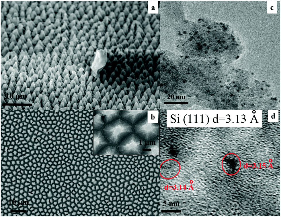 | ||
| Fig. 1 (a) SEM image of the surface morphology of the as-prepared porous silicon (53° tilted); (b) SEM top view image of the as-prepared porous silicon. Inset: magnified top view image of as-prepared porous silicon; (c) TEM image of the surface of porous silicon (the black dots observed in the image are Si nanoparticles); (d) HR-TEM image of surface morphology. Lattice fringes with distances of 3.14 and 3.15 Å can be observed in the black dots. The distances correspond to Si(111) (3.13 Å). | ||
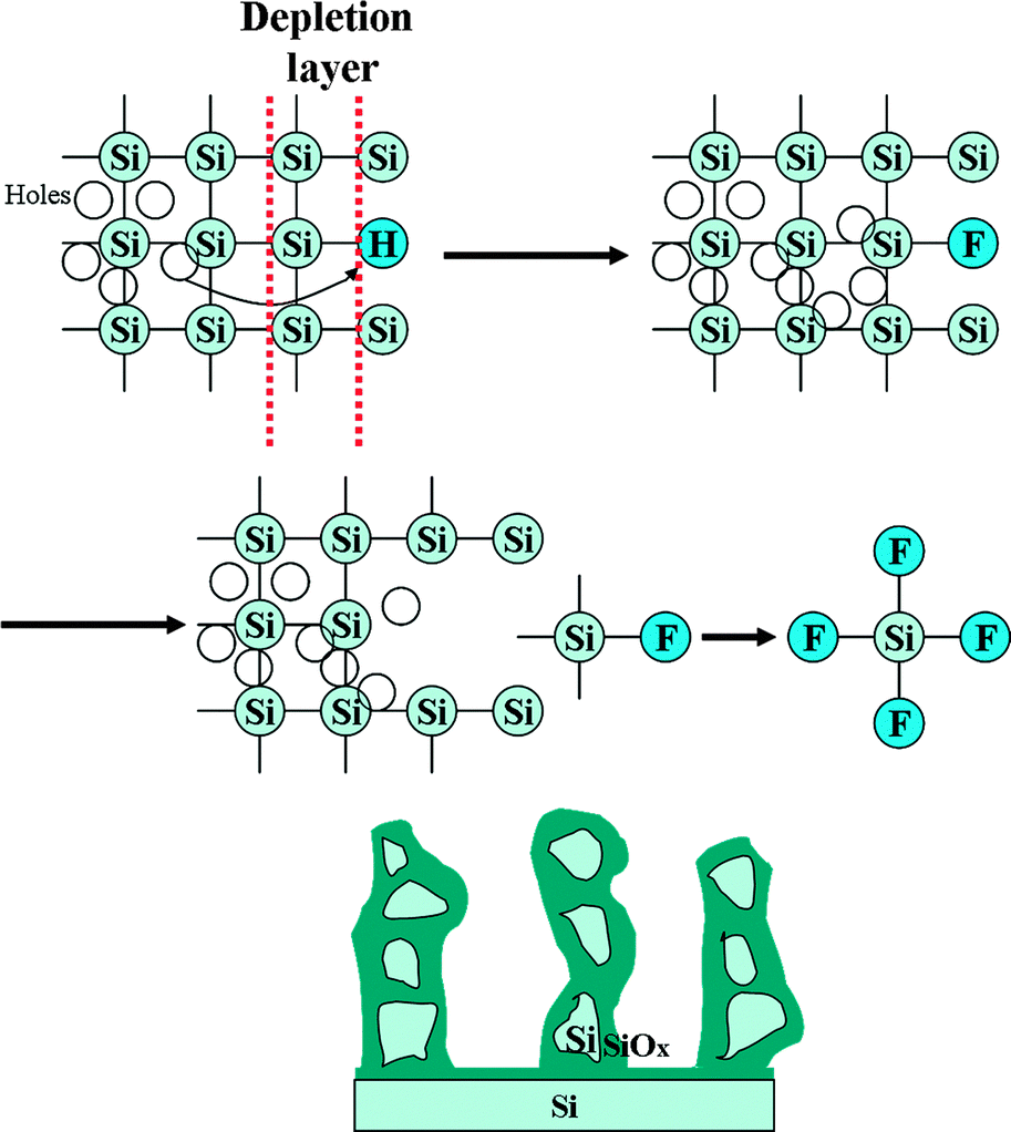
The formation mechanism of the column-shaped PSi is illustrated in Scheme 1. The electronic characteristics of the interface between the Si wafer and the electrolyte are similar to that of a P–N junction. As the Fermi levels of Si and the electrolyte are different, the diffusion of carriers happens at their interface. As a result, a depletion layer with a low carrier density will form at the Si/electrolyte interface. When an electric potential was applied, the initially passivated Si–H bonds were replaced by Si–F bonds with the aid of the holes that originated from the bulk and the oxidant (ferric nitrate). The Si–F bond has a strong polarization capacity that can weaken the Si–Si back and side bonds. As a consequence, Si atoms are dissolved due to the HF corrosion and break apart from the Si substrate. The corrosion process can be expressed as below:
| Si + 4F− + 2H+ + 2h+ = SiF4 + H2 |
 | ||
| Scheme 1 Schematic of the formation process of the prepared column-shaped PSi. | ||
Because the surface of the Si wafer is not an ideal plane, it contained some small pits on the surface. When the tip of the pit is very sharp, the sharp point will accumulate more holes than the planar areas. Thus, the corrosion rate at the sharp regions tends to be faster than at other areas. Finally, a column-shaped structure forms on the surface.
The PL spectrum of the freshly prepared PSi under the excitation wavelength of 260 nm is shown in Fig. 2a. Compared to the insignificant PL from the bulk silicon (1.12 eV),1 PSi showed a strong and wide blue-shifted peak at 667 nm (1.85 eV). This PL is usually derived from the quantum confinement effect for nanosized Si crystals (as observed in the TEM image of Fig. 1d). It has been confirmed that when the size of Si nanoparticles is <4.3 nm, their quantum confinement effect becomes more distinct.7 XPS analysis provides information about the chemical composition of the surface of PSi, as shown in Fig. 2b. The XPS wide scan confirmed that only Si, O and C are found on the surface. The Si2p peak can be deconvoluted into three peaks (Si, SiO and SiO2) in the spectrum of freshly prepared PSi (see Fig. S2a, ESI†).26 The unsaturated oxygen state (SiO) indicates the presence of oxygen defects on the surface. It is well known that oxygen defects in the form of SiOx (x < 2) play the same role as luminescence centers.26 Thus, in this case, both silicon nanostructures and oxygen defects (the interface of the Si nanoparticles/SiOx) affect the PL of PSi. However, the aging test (see Fig. S1, ESI†) indicates that the PL intensity decreases rapidly when the sample is placed under ambient air conditions. Only 25% of the PL intensity remained after one week, and the peak almost disappeared after one month (see Fig. S1, ESI†). The degradation of PL is a major obstacle for practical optoelectronic applications of PSi. The formation of SiO2 on the surface may be the reason for this degradation. The XPS spectra also indicate this phenomenon (see Fig. S2a–c, ESI†). Si was oxidized with the increase in aging time, and the Si2+ peak became weak. Only the Si4+ peak was enhanced. These results strongly confirm that the number of the PL cores of the Si nanoparticles and oxygen defects decreases due to oxidation, indicating that SiOx (x < 2) became SiO2.
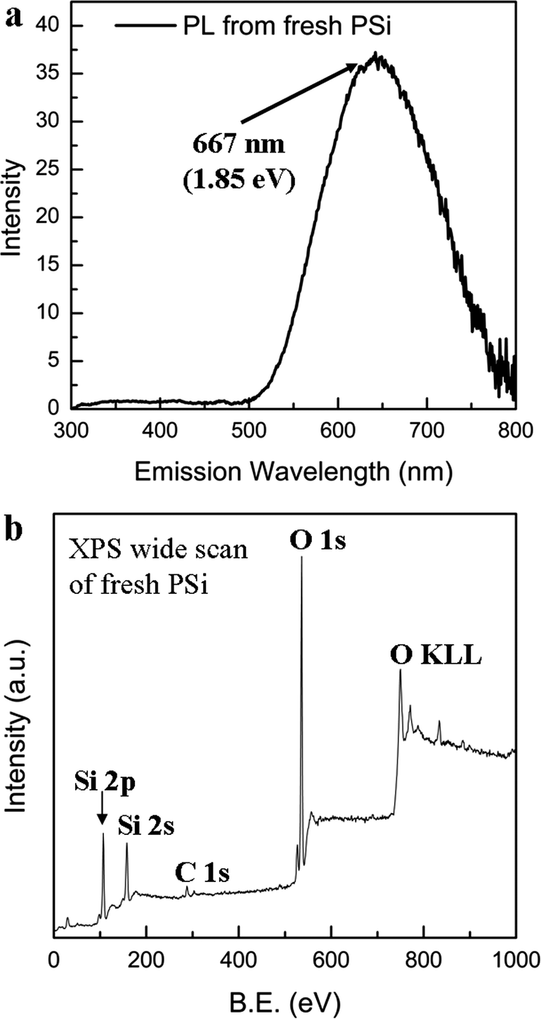 | ||
| Fig. 2 (a) Photoluminescence spectrum of freshly prepared porous silicon (excitation wavelength = 260 nm); (b) wide X-ray photoelectron spectrum (XPS) of the freshly prepared porous silicon. | ||
Although the PL of the aged PSi is seriously degraded, luminescent centres such as silicon nanoparticles are still present on the surface of the aged PSi. To improve the PL behaviour, the PL-collapsed aged (2 months in air) PSi sample was immersed in 5% HF for 5 s to remove the newly formed SiO2 thin layer on the surface. The fluorescence spectrum of the fresh HF-treated aged PSi is shown in Fig. 3a. Under 260 nm excitation, the red peak reappeared at 670 nm (the intensity of the red PL peak of fresh HF-treated aged PSi was even 10% higher than that of fresh PSi) and a new weak peak was observed at 415 nm. The PL results shown in Fig. 2a, 3a and Fig. S1 (ESI†) reveal that the major factor for the red PL in Fig. 2a originates from the oxygen defects at the Si nanoparticle/SiOx (x < 2) interface. As the exposure time of PSi in air increases, the amount of oxygen defects on the surface decreases rapidly due to oxidation; also, the size of the Si nanoparticles decreases in this process, thus decreasing the PL from PSi. The rate of oxidation of Si is significantly lower than that of SiOx (x < 2); therefore, Si nanoparticles still exist on the surface of PL-degraded age PSi, particularly after stable SiO2 dominates on the surface, because the Si nanoparticles are surrounded by SiOx (x < 2). Thus, some Si nanoparticles became smaller or were fully oxidized to form Si oxide, while another portion of the Si nanoparticles maintained their size with almost no change. After the HF treatment on the aged PSi surface, the oxygen defects were recovered at the surface of the Si nanoparticles, resulting in the reappearance of PL in the red region (Fig. 3a). Also, in general, the blue shift of the newly formed deep blue PL band (415 nm) can be attributed to the following: (i) after oxidation in air, the change in the value of x in SiOx (x < 2) changes the positions of the oxygen defect energy levels in the band gap; and (ii) the size of the Si nanoparticles is decreased by oxidation in air (the smaller the particle size, the larger the band gap). Although the PL reappeared, this HF-treated aged PSi was still very readily oxidized. To further improve the PL behaviour, a Cu coating was applied to protect the fresh HF-treated aged PSi surface from oxidation. Since the PSi has a hackly surface, the thickness of the sputtered ultrathin Cu layer (deposition rate: ca. 3.5 nm min−1) is not homogeneous (Fig. 3b, dark areas are Cu coated regions), and the diffraction pattern shows that the compositions of the Cu layer on the surface were in the form of Cu and polycrystalline Cu2O (see Fig. S3, ESI†). The PL spectra of Cu-PSi are shown in Fig. 3c and d. Fig. 3c shows that with the change in sputtering time, a significant PL dissimilarity was detected. Compared to the fresh PSi, all the Cu-coated samples showed a clear PL band with intensity change factors in the range of 0.35–4 in the blue region (470 nm) with three shoulders (460 nm, 485 nm and 496 nm) and a sub-band at ∼565 nm. Among these, the 2 min Cu-coated sample showed the strongest improvement (the PL spectra and relative characterization below refer to the 2 min Cu-coated sample unless otherwise indicated). The enhanced PL originated from Cu diffusion and the formation of new Cu-SiOx (x < 2) compounds after Cu sputtering, i.e., Cu diffused into interstitial defects in the SiOx and the unstable SiO may have combined with Cu to form Cu–SiOx (x < 2).24,25 The diffused Cu and Cu–SiOx donated new Cu-related defect sites to the Si nanoparticle/SiOx band gap. Fig. 3d shows the PL emission spectra under different excitation wavelengths from 260 to 340 nm. The blue peak position at 470 nm did not change; therefore, this peak originated from the new Cu-related defect sites and the three shoulders arose from the 3d10 → 3d94s1 transitions of Cu+.27 Because of the fixed value difference between the defect energy levels, the PL position also remains constant. However, the peak at ∼565 nm changed according to the excitation wavelength. Thus, the origin of this PL at ∼565 nm can be attributed to the remaining silicon or new Cu2O, Cu nanoparticles.
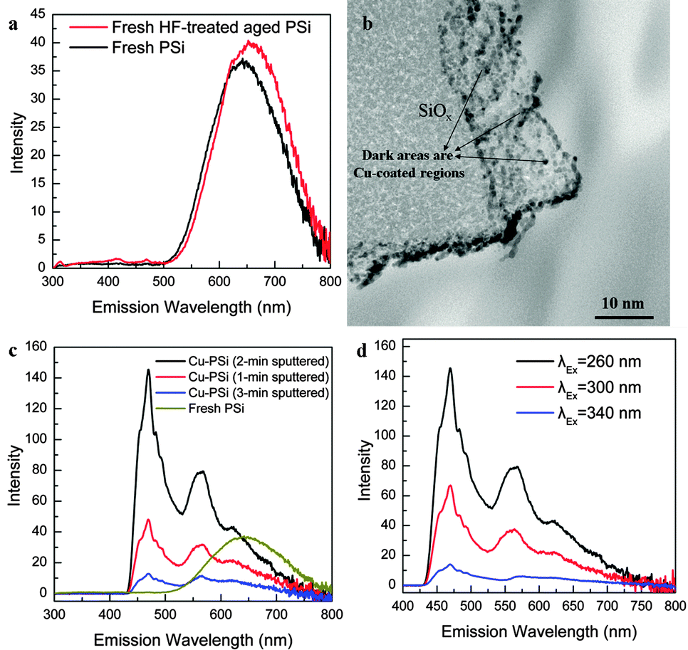 | ||
| Fig. 3 (a) Photoluminescence spectra of fresh porous silicon (PSi) (black) and fresh HF-treated aged (2 months in air) PSi (red). Excitation wavelength = 260 nm. (b) Cross-sectional TEM image of Cu-coated HF-treated aged PSi (Cu-PSi, PSi was aged in air for 2 months before sputtering). The sputtering time of Cu was 1 min. The sample was prepared using FIB (JEOL JPS-9200 X-ray photoelectron spectrometer) with a thickness of 100 nm. (c) Comparison of photoluminescence spectra of Cu-PSi samples (2 months aged in air and surface treated with HF before sputtering) under different sputtering conditions under an excitation wavelength of 260 nm. (d) Photoluminescence spectra of Cu-PSi with a sputtering time of 2 min (2 months aged in air and surface treated with HF before sputtering) under various excitation wavelengths. | ||
More PL spectra of various Cu coated porous silicon samples were measured as shown in Fig. 4. The PL intensity of Cu coated fresh porous silicon (red line) decreased to 65% of the original value, while the sample of Cu coated aged (2 months in air) porous silicon without HF treatment (blue line) had a collapsed PL in the red range. The results (blue and red lines) in Fig. 4 can be explained by the following considerations: (i) for the fresh prepared sample, the surface was passivated by –H, –OH or –CHx (H cannot be detected by XPS), so the sputtered Cu cannot efficiently contact the unstable SiO on the surface; (ii) for the aged sample, SiO2 dominated the surface state; stable SiO2 and Cu do not react at room temperature. Simultaneously, these results also demonstrated that the Cu2O and Cu nanoparticles in Fig. 3b were not the major factor causing the PL. Only Cu coated HF-treated aged porous silicon showed a PL enhancement; therefore, only this sample will be discussed below.
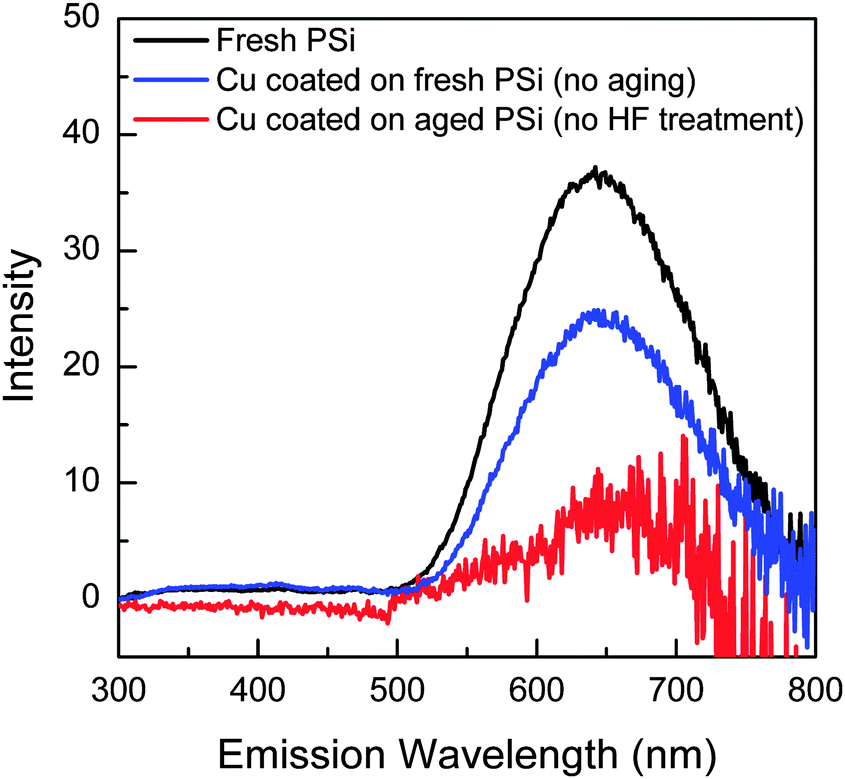 | ||
| Fig. 4 Photoluminescence spectra of various Cu coated (2 min) PSi samples under different treatment conditions (black: fresh PSi; red: Cu coated PSi, PSi was freshly prepared without aging in ambient air; blue: Cu coated PSi, PSi was aged in air for 2 months without HF treatment before Cu sputtering). Excitation wavelength = 260 nm. | ||
The PL stability of Cu-PSi is shown in Fig. 5. Unlike the severe degradation of fresh PSi, the PL intensity of Cu-PSi showed no significant change under ambient conditions for one month. Even after three months under ambient conditions, the PL intensity was very stable. This stability is due to the protection of the metal coating. The formed Cu–SiOx (x < 2) on the surface prevents the reaction between oxygen and the inner materials. However, as the oxidation time increased, the PL of Cu-PSi also degraded. In our case, Cu-PSi can maintain its intensity for at least six months.
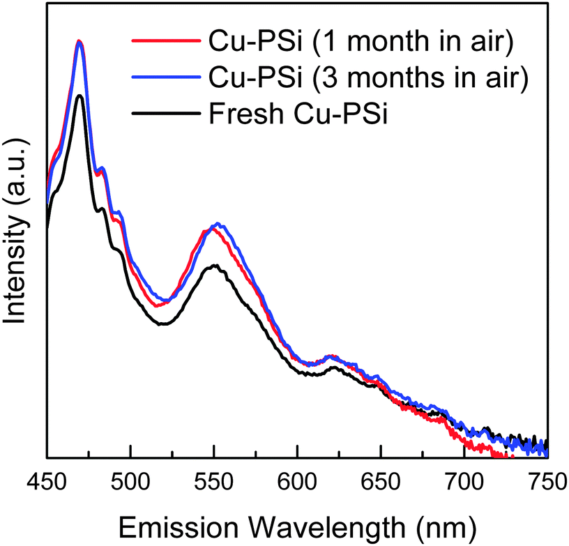 | ||
| Fig. 5 Aging effects on the photoluminescence intensity of Cu-PSi under 2 min sputtering treatment. | ||
The optical reflectance spectra of the Si samples were measured, as shown in Fig. 6, to support the PL results. Fig. 6a shows the surface reflectance spectra of PSi and planar Si. Fig. 6b provides the comparison between the Cu-PSi and PSi. The surface reflectance of PSi decreased to 5% compared to the value (∼50%) of planar Si (Fig. 6a; the sharp reflectance change at around 364 nm was caused by the change of light source). This decrease in surface reflectance can be attributed to multireflection among the surface columns. This result also demonstrated that the optical loss, which is a very important index for the optical properties of Si, decreased. The reflectance curve of Cu-PSi has a similar tendency to that of PSi. In the long-wavelength range, the reflectance of Cu-PSi is almost the same as that of PSi, while in the short-wavelength range, the deviation becomes very distinct, and the mean value of the reflectance of Cu-PSi is higher than that of PSi (Fig. 6b). Despite this, the reflectance is still significantly lower than that of planar Si. In the UV region in particular, a sudden decrease at ∼250 nm indicates an optical absorption region around this area. In fact, the results of the reflectance test are also consistent with the PL spectra shown in Fig. 3d.
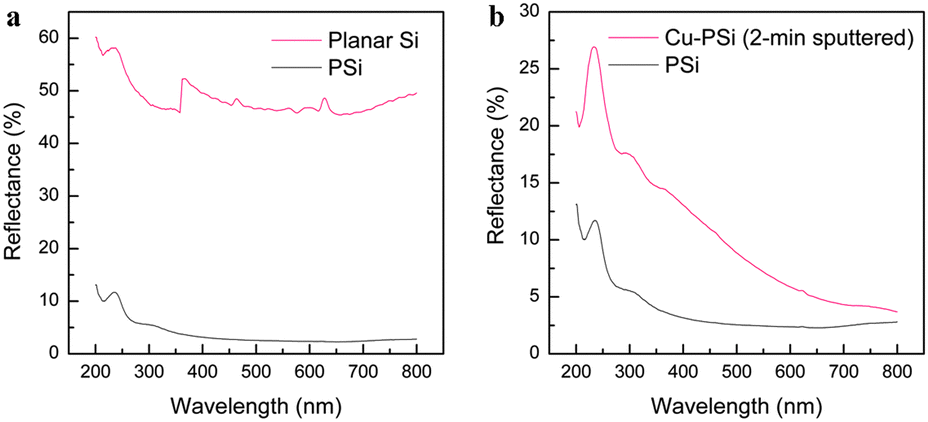 | ||
| Fig. 6 Surface reflectance spectra of porous silicon samples. (a) Surface reflectance spectra of planar Si (red) and freshly prepared porous silicon (PSi, black); (b) surface reflectance spectra of freshly prepared porous silicon (PSi, black) and Cu-coated porous silicon (Cu-PSi, red). | ||
The PL of PSi and Cu-PSi in this study can be attributed to oxygen/metal defects experiencing quantum confinement effects. Under quantum confinement conditions7 (for example: Si with the size <4.3 nm), the most significant change is that the band gap became wider than that of the bulk. Fig. 1c and d show that the PSi contains Si nanocrystals in silicon oxide side walls; these Si nanocrystals divide the continuous conduction and valence bands into isolated energy levels. After this change, the band gap became wider. For PSi, when an electron is excited, three transition paths can be considered (Fig. 7a, upper): (1) nonradiative centers (mark 1), (2) recombination with holes (mark 2), and (3) capture by interface oxygen defects (mark 3). The latter two models result in PL phenomena. For Cu-PSi, the surface SiO film is very unstable even at room temperature;24 thus, it combined with the sputtered Cu and formed a new ultra-thin compound layer. The interface structural model of Cu-PSi is shown in Fig. 7a (bottom). Simultaneously, this structure (Cu–SiOx, x < 2) can donate new Cu related defect sites to the band gap, and these Cu related defect sites are considered to be a type of PL center.28–32 To confirm the presence of Cu–SiOx (x < 2), the XPS spectra of Si2p of Cu-PSi were measured, as shown in Fig. 7b.
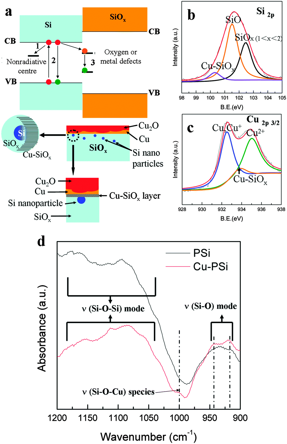 | ||
| Fig. 7 (a) Schematic of the photoluminescence mechanism of porous silicon and Cu-PSi (upper). Surface structure model of Cu-PSi (bottom); (b) XPS result of Si 2p peak for Cu-PSi (sputtering duration: 1 min); (c) XPS result of Cu 2p peak for Cu-PSi (sputtering duration: 1 min); (d) FTIR spectra of the Cu-PSi with 1 min sputtering treatment (red) and PSi (black). | ||
Compared to the XPS spectrum of fresh PSi (see Fig. S2a, ESI†), the SiO (light blue line) peak was still present, and SiO2 (black line) transformed to unsaturated silicon oxides (SiOx, 1 < x < 2). Moreover, a new peak (purple line) appeared at 100.4 eV and replaced the Si peak (99.7 eV). As the electronegativity of Cu is less than that of oxygen, the peak shifted to a lower energy when Cu reacted with SiO. This implies that the peak at 100.4 eV arose from the Cu–SiOx (x < 2) or SiOx (x < 1). Moreover, the XPS of Cu2p3/2, as shown in Fig. 7c, shows a peak at ∼933.9 eV, a typical position of Cu and Si oxide compounds.33 Based on these results, the peak at 100.4 eV can be assigned to Cu–SiOx (x < 2). However, it is very strange that the Si peak was not observed in this XPS spectrum. The most plausible reason for this absence is the detection limit: the limit of detection of our XPS device (JEOL JPS-9200) is 0.1 at% and 2–5 nm in depth. From Fig. 1d and Fig. S2a (ESI†), the surface structure of the freshly prepared PSi can be described as Si nanoparticles surrounded by amorphous Si oxides (the thickness of the Si oxide layer is about 100 nm, as shown in Fig. S4, ESI†). Thus, the relatively weak Si peak in the XPS spectrum shown in Fig. S2a (ESI†) comes from the Si nanoparticles in the Si oxide layer. Compared to Si oxides, even in the XPS spectrum of the freshly prepared PSi, the content of Si is very small. As the aging time increased in air, some of the Si nanoparticles in the Si oxide layer were oxidized, and the Si content became lower than the XPS detection limit (0.1 at%), resulting in the absence of the Si peak in the XPS spectra of the aged PSi (Fig. S2b and c, ESI†). Because the Cu-PSi was prepared using an aged PSi substrate, the reason for the absence of the Si peak in the XPS spectrum of Cu-PSi is the same as the reason for the aged PSi. Another notable phenomenon is the presence of CuO in the XPS spectrum; however, CuO was absent in the diffraction pattern. This indicates that CuO existed in the amorphous form on the surface. The existence of Cu–O–Si was also confirmed by the FTIR analysis, as shown in Fig. 7d. Three absorption bands that appeared at 930 cm−1, 1070 cm−1, and 1180 cm−1 in both the spectra were attributed to the Si–O stretching mode and the Si–O–Si asymmetric stretching modes (the latter two), respectively.34,35 Concurrently, compared to the curve of PSi (black line), the spectrum of Cu-PSi (red line) showed three new shoulders at 919 cm−1, 945 cm−1 and 1002 cm−1. These shoulders can be assigned to the perturbation of copper;34 in particular, a shoulder at 1000 cm−1 has been attributed to Si–O–Cu stretching species in previous research.36,37
4. Conclusions
In this study, a Cu-PSi composite structure with enhanced PL was developed, and the preparation did not require a high-temperature environment. Cu-PSi showed dual PL bands in the blue and yellow ranges. Compared to the PL of fresh PSi, the PL intensity of these two bands was greater. Simultaneously, the PL stability of Cu-PSi was also improved. The formation of Cu-related defect sites in the band gap of Si nanoparticles/SiOx and a less efficient oxidation process on the surface were determined as the major factors causing the enhanced PL intensity and relatively high stability. The improved fluorescence properties of PSi may extend the opportunities for Si-based optoelectronics in the future.Acknowledgements
We thank Assistant Prof. Fujita, Faculty of Engineering, Hokkaido Univ. for his kind help in the reflectance measurement. This work was partially supported by a Grant from Hokkaido University (to TY) and by a Grant-in-Aid for Scientific Research (A) (24241041, to TY). A part of this work was supported by the Nanotechnology Platform Program (Characterization and Fabrication, Hokkaido University) of the MEXT, Japan.Notes and references
- A. G. Cullis and L. T. Canham, Nature, 1991, 353, 335–338 CrossRef CAS PubMed.
- M. J. Sailor, Porous silicon in practice: preparation, characterization and applications, Wiley-VCH, Weinheim, Germany, 2012 Search PubMed.
- S. Pace, R. B. Vasani, F. Cunin and N. H. Voelcker, New J. Chem., 2013, 37, 228–235 RSC.
- S. Pace, P. Gonzalez, J. M. Devoisselle, P. E. Milhiet, D. Brunel and F. Cunin, New J. Chem., 2010, 34, 29–33 RSC.
- A. Pradeep and P. Agarwal, J. Appl. Phys., 2008, 104, 123515 CrossRef PubMed.
- L. Brus, J. Phys. Chem., 1994, 98, 3575–3581 CrossRef CAS.
- C. Delerue, G. Allan and M. Lannoo, Phys. Rev. B: Condens. Matter Mater. Phys., 1993, 48, 024–036 CrossRef.
- M. Nolan, S. O’Callaghan, G. Fagas and J. C. Greer, Nano Lett., 2007, 7, 34–38 CrossRef CAS PubMed.
- J. A. L. López, G. G. Salgado, A. P. Pedraza, D. E. V. Valerdia, J. C. Lópeza, A. M. Sáncheza, T. D. Becerrila, E. R. Andrésa and H. J. Santiesteban, Proc. Eng., 2011, 25, 304–308 CrossRef PubMed.
- Y. W. Wang, C. H. Liang, G. W. Meng, X. S. Peng and L. D. Zhang, J. Mater. Chem., 2002, 12, 651–653 RSC.
- N. Shirahata, A. Hozumi and T. Yonezawa, Chem. Rec., 2005, 5, 145–159 CrossRef CAS PubMed.
- H. P. Wang, D. H. Lien, M. L. Tsai, C. A. Lin, H. C. Chang, K. Y. Lai and J. H. He, J. Mater. Chem. C, 2014, 2, 3144–3171 RSC.
- E. Kayahan, Appl. Surf. Sci., 2011, 257, 4311–4316 CrossRef CAS PubMed.
- X. T. Zhou, R. Q. Zhang, H. Y. Peng, N. Shang, N. Wang, I. Bello, C. S. Lee and S. T. Lee, Chem. Phys. Lett., 2000, 332, 215–218 CrossRef CAS.
- B. Gelloz, A. Kojima and N. Koshida, Appl. Phys. Lett., 2005, 87, 031107 CrossRef PubMed.
- A. Daami, G. Bremond, L. Stalmans and J. Poortmans, J. Lumin., 1999, 80, 169–172 CrossRef.
- L. Lin, X. Sun, R. Tao, J. Fang and Z. Zhang, Nanotechnology, 2011, 22, 075203 CrossRef PubMed.
- Y. Fu, R. Yao and C. Cao, J. Mater. Chem. C, 2013, 1, 6422–6427 RSC.
- K. Y. Suh, Y. S. Kim and H. H. Lee, J. Appl. Phys., 2002, 91, 10206–10208 CrossRef CAS PubMed.
- P. Yang, M. K. Lü, C. F. Song, D. Xu and D. R. Yuan, Phys. Status Solidi, 2002, 231, 106–111 CrossRef CAS.
- S. L. Chen, C. C. Chu and V. K. S. Hsiao, J. Mater. Chem. C, 2013, 1, 3529–3531 RSC.
- F. Yang, S. Ma, X. Zhang, M. Zhang, F. Li, J. Liu and Q. Zhao, Superlattices Microstruct., 2012, 52, 210–220 CrossRef CAS PubMed.
- L. Samuelson, S. Nilsson, Z. G. Wang and H. J. Grimmeiss, Phys. Rev. Lett., 1984, 53, 1501–1503 CrossRef CAS.
- L. Brewer and R. K. Edwards, J. Phys. Chem., 1954, 58, 351–358 CrossRef CAS.
- A. Mesli and T. Heiser, Phys. Rev. B: Condens. Matter Mater. Phys., 1992, 45, 11632–11641 CrossRef CAS.
- H. J. Xu and X. J. Li, Opt. Express, 2008, 16, 2933–2941 CrossRef CAS.
- G. Zhang, J. Long, X. Wang, W. Dai, Z. Li, L. Wu and X. Fu, New J. Chem., 2009, 33, 2044–2050 RSC.
- M. Nakamura and S. Murakami, Jpn. J. Appl. Phys., 2010, 49, 071302 CrossRef.
- Y. M. Huang, Appl. Phys. Lett., 1996, 69, 2895–2897 Search PubMed.
- A. Carvalho, D. J. Backlund and S. K. Estreicher, Phys. Rev. B: Condens. Matter Mater. Phys., 2011, 84, 155322 CrossRef.
- N. Lopez, F. Illas and G. Pacchioni, J. Am. Chem. Soc., 1999, 121, 813–821 CrossRef CAS.
- M. Steger, A. Yang and T. Sekiguchi, J. Appl. Phys., 2011, 110, 081301 CrossRef PubMed.
- S. B. Jung, H. H. Park and H. C. Kim, Thin Solid Films, 2004, 447–448, 575–579 CrossRef CAS PubMed.
- W. Lin and H. Frei, J. Phys. Chem. B, 2005, 109, 4929–4935 CrossRef CAS PubMed.
- D. B. Mawhinney, J. A. Glass and J. T. Yates, J. Phys. Chem. B, 1997, 101, 1202–1206 CrossRef CAS.
- M. Dai, J. Kwon, M. D. Halls, R. G. Gordon and Y. J. Chabal, Langmuir, 2010, 26, 3911–3917 CrossRef CAS PubMed.
- M. Dai, J. Kwon, E. Langereis, L. Wielunski, Y. J. Chabal, Z. Li and R. G. Gordon, ECS Trans., 2007, 11, 91–101 CAS.
Footnote |
| † Electronic supplementary information (ESI) available: PL aging testing and narrow X-ray photoelectron spectra of PSi, electron diffraction pattern of Cu-coated HF treated aged PSi, TEM lateral images of Cu-PSi. See DOI: 10.1039/c5nj00909j |
| This journal is © The Royal Society of Chemistry and the Centre National de la Recherche Scientifique 2015 |