
 Open Access Article
 This Open Access Article is licensed under a
 Creative Commons Attribution 3.0 Unported Licence
Band alignment of the hybrid halide perovskites CH3NH3PbCl3, CH3NH3PbBr3 and CH3NH3PbI3
Keith T.
Butler
,
Jarvist M.
Frost
and
Aron
Walsh
*
Centre of Sustainable Chemical Technology and Department of Chemistry, University of Bath, Claverton Down, Bath BA2 7AY, UK. E-mail: a.walsh@bath.ac.uk
First published on 28th October 2014
Abstract
Organic–inorganic halide perovskites efficiently convert sunlight to electricity in solar cells. The choice of halide (Cl, Br or I) can be used to chemically tune the spectral response of the materials and the positions of the valence and conduction bands (i.e. the ionisation potential and electron affinity). Here the band offsets of the methylammonium lead halides are reported, including relativistic corrections and using the Pb 1s core level as a reference state. The binding energy of the valence band decreases monotonically down the series, primarily due to the change from 3p to 4p to 5p valence orbitals of the halide. Type I band alignments are predicted, which implies that Br and Cl secondary phases in CH3NH3PbI3 thin-films would act as barriers to charge transport in photovoltaic devices.
Conceptual insightsAbsolute band edge positions determine the stability and transport of electrons and holes in materials and devices. Hybrid perovskites demonstrate electronic band offset features analogous to conventional inorganic semiconductors. Here, the valence band (ionisation potential) and conduction band (electron affinity) energies are dictated by the atomic orbitals of the anions and cations, respectively. Band energy and band gap engineering of these organic–inorganic solids is possible by controlling the chemical composition, which is crucial for extending the range of applications of hybrid perovskites beyond photovoltaics. |
Organic–inorganic perovskites can be formed by the isovalent substitution of an elemental ion by a molecular ion in the perovskite crystal structure.1 The essential physicochemical characteristics of inorganic perovskite materials are maintained in the hybrid systems, in particular structural phase transitions, lattice polarization and complex defect reactions. Since the report of solar-to-electricity conversion in 2009,2 the performance of hybrid halide perovskites has rapidly increased making them strong competitors to more mature photovoltaic technologies.3–7 The literature on photovoltaic device preparation and architectures is already immense, which is supported by a growing number of fundamental theoretical and computational efforts.8–10 The importance of relativistic effects11–13 (spin–orbit coupling) and molecular orientation effects,14–16 are two particular insights; however, many questions relating to the basic physical chemistry of these materials remain to be answered.
The most studied material has been CH3NH3PbI3 (MAPI) as it has a band gap (ca. 1.6 eV) well matched for a single-junction solar cell configuration and it is more chemically robust than the SnII analogues. MA refers to the methylammonium (CH3NH3+) cation. The optical absorption onset is blue shifted (larger band gaps) for the isostructural bromide and chloride compounds, which makes them of interest for multi-junction and semi-transparent photovoltaic applications.17 In addition, PbCl2 is commonly used as a precursor to obtain the iodide, with the presence of secondary chloride phases a possibility. The inclusion of mixed halides in hybrid perovskite absorbers has been studied from several perspectives and offers control over several important characteristics of the materials and devices. Improved carrier lifetimes are obtained with the increased crystal quality associated with the presence of Cl, possibly through partial substitution of I in the lattice,18–20 which has been attributed to reduced bi-molecular recombination rates.21 Tuning of optical absorption spectra due to band gap modification has also been reported in several studies.8,17,20,22 The analogous bromide based devices display larger open circuit voltages23 and improved device lifetimes.20
Beyond band gap changes, knowledge of the variation in the valence and conduction band levels is critical for optimization of new device configurations. Energy level offsets of mixed halide perovskites have been studied using photoemission spectroscopy.24 Based on these band energy offsets, devices with hole transport layers replaced by MAPbBr3 have been reported.25 In this communication, we report the extension of a core-level alignment technique to hybrid perovskites systems and predict the natural band offset of the CH3NH3PbX3 (X = Cl, Br, I) series. The results provide insights into the relative electronic chemical potentials of these materials and a general approach that can be applied to other perovskite-structured compounds. They constitute a first step towards understanding the interfacial electronic structure likely to be found in real devices.
The success of electronic structure techniques for modelling bulk crystal properties is well documented.26,27 One distinction from molecular quantum chemical calculations is the absence of a vacuum level. Within periodic boundary conditions the electronic band structure is given on an energy scale that is relative to an internal reference, which is system (compositionally and structurally) dependent.28 For example, in the density functional theory code VASP,29 the average electrostatic (Hartree) potential in the unit cell is set to 0 V for every system. The problem is longstanding and various approaches for computing absolute valence and conduction band positions have been recently discussed.30–32 We reported an approach for determining the ionisation potentials of porous metal–organic frameworks;33 however, the charged molecules inside the hybrid perovskite cage structure makes the approach inapplicable here.
A convenient computational approach, widely applied to close-packed semiconductors, is core-level alignment.34 A three-step procedure is generally adopted, similar to that used in X-ray photoemission spectroscopy (XPS):35–37
(1) Calculate the energy separation between a reference core state and the upper valence band of two isolated reference materials (A and B). These values are intrinsic to a bulk material and cannot be compared directly between different compounds.
(2) Align the two reference states on each side of a heterojunction formed between materials A and B (ΔEC in Fig. 1). The reference states are taken at the centre of each layer.
 | ||
| Fig. 1 Schematic alignment procedure used to calculate the natural valence band offsets for the hybrid perovskites. For example, to calculate the MAPbI3/MAPbBr3 offset three separate electronic structure calculations are performed: (i) bulk MAPbI3 to obtain core and valence band eigenvalues; (ii) bulk MAPbBr3 to obtain core and valence band eigenvalues; (iii) a MAPbBr3/MAPbI3 heterostructure to obtain core levels at the centre of each layer and their energy difference (ΔEC). The valence band positions of the isolated materials are then aligned with respect to the Pb 1s core levels (at a binding energy of approximately 8800 eV) to produce the final valence band offsets of the isolated materials (ΔEV). | ||
(3) Compute the “natural” valence band offset (ΔEV in Fig. 1), which minimizes interface-specific effects, by summing up the two contributions listed above. The isolated core–valence band energies from (1) are aligned using the offset in core levels from (2).
The process is shown schematically in Fig. 1. The principal approximation is that the chosen core level is a reliable reference state, which may not be the case for semi-core (e.g. 3d) levels. An advantage of computation over experiment is that extremely deep atomic-like states can be chosen, e.g. in this study we use Pb 1s (within a projector augmented wave (PAW)38 formalism that includes the response to the self-consistent valence electron density) that is inaccessible using standard X-ray sources. The success of this approach is well documented,39 and similar results can be obtained using the spherical or planar averaged electrostatic potential as a reference.40,41
Two convenient aspects of the chosen approach are that the calculated natural band offsets satisfy the transitivity relation (i.e. if the offsets of A/B and A/C are known, then B/C can be inferred with good accuracy) and the values converge quickly with respect to system size. It should be noted that interfacial states are explicitly avoided. The associated transferability of the values computed (or measured) are useful to rationalise the behaviour of a particular combination of materials, or the design of optimal systems, but they should not be expected to be quantitative for predicting the properties of a specific interface, which may be subject to gradients in composition and/or local structure variations.
Heterostructures for mixed Cl/Br and Br/I systems were constructed using 1 × 1 × 4 supercell expansions of the equilibrium perovskite structure (from fully relaxed internal coordinates). The lattice parameters were fixed to the average of the two component materials. The electrostatic potential was checked to ensure no macroscopic dipole was formed across the interface. The electronic structure was calculated using density functional theory within the code VASP. The PBEsol42 exchange-correlation functional was employed which describes well both the lattice constants and the electrostatic interactions between the three perovskite components (the methylammonium cation and the negatively charged cage formed of lead and halide ions). The core electrons were treated using PAW, which accounts for scalar-relativistic effects, and the valence electrons were represented using a plane wave basis set (500 eV kinetic energy cut-off). The contributions to the valence band structure from spin–orbit coupling were determined perturbatively. While a many-body description of the electronic structure has been found to be necessary to provide quantitative electronic properties (e.g. effective masses and high-frequency dielectric functions), the quasi-particle corrections to the absolute valence band position are small.8 The predicted alignments, including these corrections, are expected to be accurate to within 0.1 eV.
The computed pseudo-cubic lattice constants of the chloride, bromide and iodide hybrid perovskites are 5.68, 5.92 and 6.29 Å, respectively. The Cl/Br and Br/I heterostructures are formed using the average lattice constants of 5.80 and 6.10 Å, respectively, which results in a lattice mismatch of 3% or less for each material, within the limits for coherent, defect-free interface formation. The results, following the procedure outlined above, are summarized in Fig. 2. It should be noted that the band gap deformation potential for each material is positive (i.e. a lattice contraction results in a band gap decrease).14 For example, the calculated deformation potential of 2.5 eV for MAPbI3 implies that a hydrostatic contraction of the lattice by 10% volume would result in a band gap reduction of 0.25 eV. This factor is however secondary to the chemical differences of the halides, as discussed below.
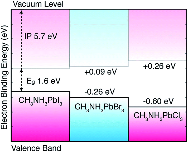 | ||
| Fig. 2 Calculated valence band alignment of three pseudo-cubic hybrid halide perovskites. The equilibrium crystal structures are provided in an online repository.51 The energies are given with respect to the band edge positions of CH3NH3PbI3 previously reported including corrections from quasi-particle self-consistent GW theory.11 | ||
In the hybrid perovskites, the formal electronic configuration of Pb(II) is 6s26p0, while for the halides it is np6. It is therefore not surprising that the upper valence band is dominated by the halide p orbital (with minor anti-bonding contributions from Pb 6s2 following the revised lone pair model43) and the conduction band is formed of a network of Pb 6p orbitals. The molecular cation does not directly contribute to the electronic band edges,44,45 but can be used to influence the crystal structure and change the band gap indirectly. For this reason, the valence band position is sensitive to the choice of halide: on transition from Cl to Br to I, the valence atomic orbitals change from 3p to 4p to 5p. To consider the contribution from the atomic energy level shifts, we calculate the electronic structure of the isolated halide ions in vacuum. Here we can use a high level theory: coupled cluster with singles and double excitations (CCSD) with a QZVP basis set. Calculating the anion in a spin singlet configuration, we arrive at energies for the highest occupied orbital of −3.64, −3.94 and −4.36 eV on the series I to Cl. The large atomic decrease in binding energy with increasing principal quantum number is mirrored in the solid-state: there is a monotonic increase in the binding energy of the valence band from I to Cl. Ultraviolet photoemission spectroscopy (UPS) measurements confirm this trend for the valence bands of the Br and I perovskites;24 while a quantitative comparison is tempting, the experiment concerns surface states, which are notoriously sensitive to sample preparation and environment.
The predicted band alignment provides insights into the spectral blue-shift observed for the isolated perovskites, as well as the I/Br and I/Cl solid-solutions.17,20 The band gap increase from I to Br to Cl is predominately driven by the valence band downshift, with the conduction band upshift less pronounced. This behavior results in type I offsets between each material, e.g. an interface between CH3NH3PbI3 and CH3NH3PbCl3 would result in electron and hole confinement in the iodide layer, with the chloride acting as a barrier to electron and hole transfer. However, due to the asymmetry of the offset, hole blocking should be more significant than electron blocking. Effective two-dimensional quantum well structures could be constructed from mixed-halide superlattices, which is of particular interest with the recent report of tuneable Dresselhaus (relativistic) splitting of the band edge states.11,46 The relative alignments calculated between CH3NH3PbI3 and CH3NH3PbBr3 are in good agreement with UPS24 measurements, as well as being consistent with a recently proposed device architecture where the hole transporting layer can be replaced by CH3NH3PbBr3 due to the advantageous offset between the two phases.25
In summary, we have provided quantitative insights into the nature of the electronic alignment between the methylammonium lead halide perovskites. The results suggest that the observed variations in the band gap are driven by changes in the valence band, and that type I (electron and hole confining) offsets are formed for each material combination. Interfacial engineering47–49 could be used to alter these “natural” alignments, e.g. through the use of dipolar layers commonly employed in organic photovoltaics or indeed through structural modification of the perovskites themselves. Initial predictions of ferroelectric tendencies in hybrid perovskites14,16 have recently been observed experimentally.50 These will likely be fruitful avenues of research. Similar trends are expected for other counter ions in the perovskite structure as the changes are driven by the chemistry of the halide ions that form the upper valence band.
Acknowledgements
We acknowledge membership of the U.K. HPC Materials Chemistry Consortium, which is funded by EPSRC Grant EP/L000202. J.M.F. and K.T.B. are funded by EPSRC Grants EP/K016288/1, EP/M009580/1 and EP/J017361/1. A.W. acknowledges support from the Royal Society and the ERC (Grant 277757).References
- D. Weber, Z. Naturforsch., 1978, 33b, 1443–1445 CAS.
- A. Kojima, K. Teshima, Y. Shirai and T. Miyasaka, J. Am. Chem. Soc., 2009, 131, 6050–6051 CrossRef CAS PubMed.
- H.-S. Kim, C.-R. Lee, J.-H. Im, K.-B. Lee, T. Moehl, A. Marchioro, S.-J. Moon, R. Humphry-Baker, J.-H. Yum, J. E. Moser, M. Grätzel and N.-G. Park, Sci. Rep., 2012, 2, 591 Search PubMed.
- R. F. Service, Science, 2014, 344, 458 CrossRef PubMed.
- H. J. Snaith, J. Phys. Chem. Lett., 2013, 4, 3623–3630 CrossRef CAS.
- N. N. Park, J. Phys. Chem. Lett., 2013, 4, 2423–2429 CrossRef CAS.
- J.-H. Im, C.-R. Lee, J.-W. Lee, S.-W. Park and N.-G. Park, Nanoscale, 2011, 3, 4088–4093 RSC.
- E. Mosconi, A. Amat, M. K. Nazeeruddin, M. Grätzel and F. De Angelis, J. Phys. Chem. C, 2013, 117, 13902–13913 CAS.
- F. Brivio, A. B. Walker and A. Walsh, APL Mater., 2013, 1, 042111 CrossRef PubMed.
- W.-J. Yin, T. Shi and Y. Yan, Appl. Phys. Lett., 2014, 104, 063903 CrossRef PubMed.
- F. Brivio, K. T. Butler, A. Walsh and M. van Schilfgaarde, Phys. Rev. B: Condens. Matter Mater. Phys., 2014, 89, 155204 CrossRef.
- P. Umari, E. Mosconi and F. De Angelis, Sci. Rep., 2014, 4, 4467 Search PubMed.
- J. Even, L. Pedesseau, J.-M. Jancu and C. Katan, J. Phys. Chem. Lett., 2013, 4, 2999–3005 CrossRef CAS.
- J. M. Frost, K. T. Butler, F. Brivio, C. H. Hendon, M. van Schilfgaarde and A. Walsh, Nano Lett., 2014, 14, 2584–2590 CrossRef CAS PubMed.
- A. Amat, E. Mosconi, E. Ronca, C. Quarti, P. Umari, M. K. Nazeeruddin, M. Grätzel and F. De Angelis, Nano Lett., 2014, 14, 3608 CrossRef CAS PubMed.
- J. M. Frost, K. T. Butler and A. Walsh, APL Mater., 2014, 2, 081506 CrossRef PubMed.
- J. H. Noh, S. H. Im, J. H. Heo, T. N. Mandal and S. I. Seok, Nano Lett., 2013, 13, 1764–1769 CAS.
- P. Docampo, F. Hanusch, S. D. Stranks, M. Döblinger, J. M. Feckl, M. Ehrensperger, N. K. Minar, M. B. Johnston, H. J. Snaith and T. Bein, Adv. Energy Mater., 2014, 4, 1400355 Search PubMed.
- S. Colella, E. Mosconi, P. Fedeli, A. Listorti, F. Gazza, F. Orlandi, P. Ferro, T. Besagni, A. Rizzo, G. Calestani, G. Gigli, F. De Angelis and R. Mosca, Chem. Mater., 2013, 25, 4613–4618 CrossRef CAS.
- B. Suarez, V. Gonzalez-Pedro, T. S. Ripolles, R. S. Sánchez, L. A. Otero and I. Mora-Sero, J. Phys. Chem. Lett., 2014, 5, 1628 CrossRef CAS.
- C. Wehrenfennig, G. E. Eperon, M. B. Johnston, H. J. Snaith and L. M. Herz, Adv. Mater., 2014, 26, 1584–1589 CrossRef CAS.
- J. Feng and B. Xiao, J. Phys. Chem. Lett., 2014, 5, 1278–1282 CrossRef CAS.
- E. Edri, S. Kirmayer, M. Kulbak, G. Hodes and D. Cahen, J. Phys. Chem. Lett., 2014, 5, 429–433 CrossRef CAS.
- P. Schulz, E. Edri, S. Kirmayer, G. Hodes, D. Cahen and A. Kahn, Energy Environ. Sci., 2014, 7, 1377–1381 CAS.
- S. Aharon, B.-E. Cohen and L. Etgar, J. Phys. Chem. C, 2014, 118, 17160 CAS.
- C. R. A. Catlow, Z. X. Guo, M. Miskufova, S. A. Shevlin, A. G. H. Smith, A. A. Sokol, A. Walsh, D. J. Wilson and S. M. Woodley, Philos. Trans. R. Soc., A, 2010, 368, 3379–3456 CrossRef CAS PubMed.
- M. C. Payne, M. P. Teter, D. C. Allan, T. A. Arias and J. D. Joannopoulos, Rev. Mod. Phys., 1992, 64, 1045 CrossRef CAS.
- J. Ihm, A. Zunger and M. Cohen, J. Phys. C: Solid State Phys., 1979, 12, 4409 CrossRef CAS.
- G. Kresse and J. Furthmüller, Phys. Rev. B: Condens. Matter Mater. Phys., 1996, 54, 11169 CrossRef CAS.
- A. Walsh and K. T. Butler, Acc. Chem. Res., 2014, 47, 364–372 CrossRef CAS PubMed.
- A. Grüneis, G. Kresse, Y. Hinuma and F. Oba, Phys. Rev. Lett., 2014, 112, 096401 CrossRef.
- Y. Hinuma, A. Grüneis, G. Kresse and F. Oba, Phys. Rev. B: Condens. Matter Mater. Phys., 2014, 90, 155405 CrossRef.
- K. T. Butler, C. H. Hendon and A. Walsh, J. Am. Chem. Soc., 2014, 136, 2703–2706 CrossRef CAS PubMed.
- A. Walsh, J. L. F. Da Silva and S.-H. Wei, J. Phys.: Condens. Matter, 2011, 23, 334210 CrossRef PubMed.
- D. O. Scanlon, C. W. Dunnill, J. Buckeridge, S. A. Shevlin, A. J. Logsdail, S. M. Woodley, C. R. A. Catlow, M. J. Powell, R. G. Palgrave, I. P. Parkin, G. W. Watson, T. W. Keal, P. Sherwood, A. Walsh and A. A. Sokol, Nat. Mater., 2013, 12, 798 CrossRef CAS PubMed.
- J. P. Bosco, S. B. Demers, G. M. Kimball, N. S. Lewis and H. A. Atwater, J. Appl. Phys., 2012, 112, 093703 CrossRef PubMed.
- V. Krishnakumar, K. Ramamurthi, A. Klein and W. Jaegermann, Thin Solid Films, 2009, 517, 2558–2561 CrossRef CAS PubMed.
- G. Kresse and D. Joubert, Phys. Rev. B: Condens. Matter Mater. Phys., 1999, 59, 1758 CrossRef CAS.
- S. Picozzi, A. Continenza and A. Freeman, Phys. Rev. B: Condens. Matter Mater. Phys., 1995, 52, 5247–5255 CrossRef CAS.
- C. G. V. de Walle and R. M. Martin, Phys. Rev. B: Condens. Matter Mater. Phys., 1987, 35, 8154 CrossRef.
- M. Peressi, J. Phys. D: Appl. Phys., 1998, 31, 1273–1299 CrossRef CAS.
- J. P. Perdew, A. Ruzsinszky, G. I. Csonka, O. A. Vydrov, G. E. Scuseria, L. A. Constantin, X. Zhou and K. Burke, Phys. Rev. Lett., 2008, 100, 136406–136414 CrossRef.
- D. J. Payne, R. G. Egdell, A. Walsh, G. W. Watson, J. Guo, P.-A. Glans, T. Learmonth and K. E. Smith, Phys. Rev. Lett., 2006, 96, 157403 CrossRef CAS.
- F. Brivio, A. B. Walker and A. Walsh, APL Mater., 2013, 1, 042111 CrossRef PubMed.
- I. Borriello, G. Cantele and D. Ninno, Phys. Rev. B: Condens. Matter Mater. Phys., 2008, 77, 235214 CrossRef.
- M. Kim, J. Im, A. J. Freeman, J. Ihm and H. Jin, Proc. Natl. Acad. Sci. U. S. A., 2014, 111, 6900 CrossRef CAS PubMed.
- K. T. Butler, J. Buckeridge, C. R. A. Catlow and A. Walsh, Phys. Rev. B: Condens. Matter Mater. Phys., 2014, 89, 115320 CrossRef.
- A. L.-S. Chua, N. a. Benedek, L. Chen, M. W. Finnis and A. P. Sutton, Nat. Mater., 2010, 9, 418–422 CrossRef CAS PubMed.
- M. Graetzel, R. A. J. Janssen, D. B. Mitzi and E. H. Sargent, Nature, 2012, 488, 304–312 CrossRef CAS PubMed.
- Y. Kutes, L. Ye, Y. Zhou, S. Pang, B. D. Huey and N. P. Padture, J. Phys. Chem. Lett., 2014, 5, 3335–3339 CrossRef CAS.
- https://github.com/WMD-Bath/Hybrid-perovskites, accessed 1st October 2014.
| This journal is © The Royal Society of Chemistry 2015 |