
 Open Access Article
 This Open Access Article is licensed under a Creative Commons Attribution-Non Commercial 3.0 Unported Licence
Capturing molecules with plasmonic nanotips in microfluidic channels by dielectrophoresis
Christian
Schäfer
,
Dieter P.
Kern
and
Monika
Fleischer
*
Eberhard Karls Universität Tübingen, Institute for Applied Physics and Center LISA+, Auf der Morgenstelle 10, 72076 Tübingen, Germany. E-mail: monika.fleischer@uni-tuebingen.de
First published on 18th December 2014
Abstract
Over the last decades, different concepts have been established for the use of plasmonic nanostructures in sensing applications. One challenge in this context lies in delivering the analyte of interest to the location of the nanostructures and selectively attaching it to their surfaces. Here we present a method for the collection and concentration of molecules on arrays of metallic nanocones, making use of the high electric field gradients at the nanotips. For this purpose, the nanocones are integrated into a microfluidic channel and used as nanoelectrodes. By applying an AC voltage, dielectrophoresis is used to capture molecules from the channel region near the nanocones. Simulations of the dielectrophoretic forces in the channel are presented as well as experimental proof of the proposed method. After attachment of the molecules, optical read-out techniques can directly be performed on the plasmonic nanostructures.
Introduction
The ability to concentrate light into nanoscale electromagnetic hot spots has given rise to many applications of plasmonic nanostructures and has led to immense interest in such structures for many years now. Under suitable excitation, localized plasmons are excited in metallic nanostructures, resulting in strong near-fields in close proximity to the structure surfaces. These strong electromagnetic fields can be used to manipulate and under suitable conditions to enhance the optical signal of particles or molecules within such an electromagnetic hot spot.1–3 They can thus be employed to improve the sensitivity of optical detection techniques. There are mainly two mechanisms used for sensing with metallic nanostructures: sensing of molecules by surface enhanced Raman spectroscopy (SERS) and sensing by observation of the shift in the particle plasmon resonance (localized surface plasmon resonance, LSPR) or Fano resonance of coupled particles.4–9 One of the main advantages of plasmonic structures is that the electromagnetic fields are confined to ultra-small volumes, which at the same time poses a big challenge for many applications. In biosensing applications, e.g., a common problem is the analysis of liquid samples with low concentrations of particles or molecules. If the molecules are distributed homogeneously in the liquid only very few molecules are located sufficiently close to the plasmonic nanostructures to be detected via the near-field. In a sensor based on plasmonic nanostructures, the challenge thus is to find a way to deliver the particles or molecules to the hot spots close to the surface of the plasmonic nanostructure, where one can take advantage of their interaction with the strong electromagnetic fields.For this purpose, typically a micro- or nanofluidic channel is used. For example, suspensions of analyte and gold nanoparticles have been introduced into a microfluidic channel with a decreasing diameter for the sensing of β-amyloid.8 Nanofluidic channels have been used to transport molecules into the hot spots of bowtie antennas.10
For a liquid with test molecules flowing through nanoholes in a gold layer, a shift of the plasmon resonance has been observed, depending on the molecule concentration of the analyte.11
Nanoelectrodes in many different configurations have been used for the accumulation of particles and molecules. As an example, nanoparticle networks have been introduced into the gaps of nanoantennas by chemical self-assembly of nanoparticles with ligands.12 By applying a DC voltage, it has been shown that single polarizable nanoparticles can be trapped in the nanogaps between electrodes, and their conductance was verified by transport measurements.13 Alternatively, dielectrophoresis (DEP) using AC voltages is extensively used for capturing, e.g. DNA and other proteins, carbon nanotubes, bacteria and viruses, or polymer beads, using standard planar gap electrodes, interdigitated nanoelectrodes, opposing triangular nanoelectrodes, 3D vertical nanopillars, and other geometries.14–18 Due to their nanoscale dimensions, carbon nanotubes and nanofibers in both horizontal and vertical configurations have been successfully applied as nanoelectrodes with strong field gradients.19–21 The scalability of the approach has been demonstrated down to single molecule trapping by nanoelectrodes.22,23 DEP is an established method for positioning micro- and nanoparticles.24–26 The DEP force depends on the third power of the radius a of polarizable particles and the gradient of the electric field squared, and can be calculated for spherical particles as:27,28
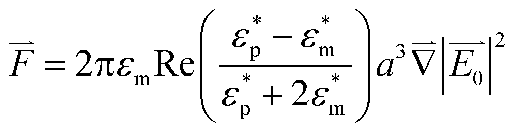 | (1) |
In several recent publications, the dielectrophoretic manipulation of biomolecules or bacteria has been successfully combined with the subsequent read-out by SERS.30–35
Here we present a method for the concentration of molecules on plasmonic nanostructures, in particular gold nanocones, by DEP. In our approach, the distance between the electrodes is in micrometers, but the strongly inhomogeneous electric field at the tips of the nanocones is exploited for capturing nanometer sized molecules.
Metallic nanocones exhibit strong electromagnetic fields near their tips under suitable laser excitation and are therefore excellent candidates for sensing applications. Their plasmon resonances have been studied in detail, and their potential as SERS substrates has been shown by the authors.36,37Fig. 1 shows the scanning electron microscopy (SEM) images of arrays of metallic nanocones with different spacings. Apart from offering the possibility to enhance the Raman signal of molecules, here the high field intensities at the nanocone tips are also used for attracting particles or molecules in the first place. For this purpose, we integrate gold nanotips fabricated on a conductive substrate (indium tin oxide (ITO) covered glass slide) into a microfluidic channel. The channel is sealed with another conductive cover slide. The substrate with the nanocones and the cover are then electrically contacted, and an AC voltage is applied. Fig. 2a) shows a scheme of this set-up (not to scale). By applying a voltage, the sharp tip of the gold nanocone acts as a lightning rod surrounded by strong field gradients, which are necessary for particle attraction by dielectrophoresis. Fig. 2b) shows an optical image of arrays of nanocones integrated into a microfluidic channel. The dielectric force created by the electric field gradients is used in order to attract particles or molecules.
 | ||
| Fig. 1 SEM images of arrays of gold nanocones with different cone distances: a) 1 μm, b) 500 nm, c) 250 nm, and d) 125 nm. Viewing angle: 70° to the surface normal for a) and 60° for b), c) and d). | ||
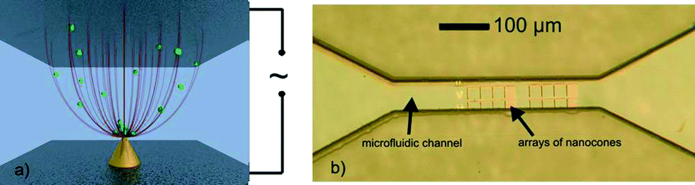 | ||
| Fig. 2 a) Schematic of the capture of particles by a metallic nanocone via dielectrophoresis (not to scale). The ITO electrode (grey) with the gold cone and the top ITO electrode are electrically contacted (AC voltage). The particles in the solution (green) are polarized and follow the gradient of the electric field squared (indicated as red lines). b) Top view of arrays of gold nanocones in a microfluidic channel (optical microscope image). | ||
Experimental
Gold nanocones can be fabricated by different processes, depending on the application. The fabrication processes developed by the authors are based on the transfer of circular etch masks into a gold layer by argon ion milling, during which the conical shape of the nanostructures is formed.36–39 The (25 μm)2 arrays of gold nanocones with different distances between the cones used in this study are fabricated by applying electron beam lithography using PMMA (polymethyl methacrylate) for the preparation of Al2O3 etch masks by a lift-off process.40,41The samples with the arrays of gold nanocones are integrated into a microfluidic channel to allow for the handling of small amounts of solutions, and to be able to use the cone substrate and the cover of the channel as electrodes. The steps of the fabrication process are displayed in Fig. 3.
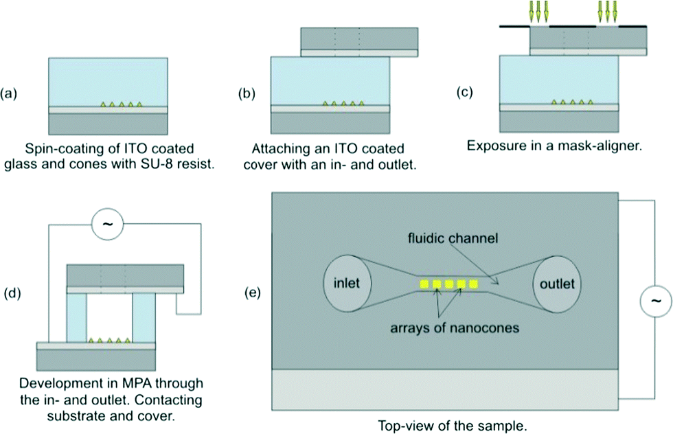 | ||
| Fig. 3 Schematic of the fabrication process for the integration of a nanocone electrode and counter electrode into a microfluidic channel. a)–d) Side view and e) top view of the sample. | ||
A layer of the epoxy resin SU-8 is spin-coated onto the sample with the nanocones on an ITO-coated glass substrate (Fig. 3a). The thickness of the SU-8 layer determines the height of the fluidic channel. Channel heights between 2 and 20 μm were used. Since the substrate and the cover of the channel will be used as the electrodes in the DEP experiment, a lower channel height leads to higher gradients of the electric field and a higher DEP force. For lower channel heights, experimental difficulties rise however, since the probability for a short circuit between the two large area electrodes with the SU-8 insulator in between increases.
As the next step, a glass slide covered with a 50 nm thick layer of ITO and two holes which will be used as the in- and outlet of the fluidic channel is carefully placed on the SU-8 covered nanocone sample (Fig. 3b). The microfluidic channel is subsequently exposed around the position of the nanocone array in a mask-aligner (Fig. 3c) through the transparent substrate. The development of the SU-8 takes place through the in- and outlet of the fluidic channel using methoxypropyl acetate (MPA, Fig. 3d). The exposure through the substrate and development of the fluidic channel through the in- and outlet have the advantage that the channel does not need to subsequently be sealed to make it leak-proof. If alternatively the cover was glued on the finished channel with a thin SU-8 layer, the SU-8 would cover the top electrode as well. For this reason, the exposure and development of the channel are performed after gluing the cover on. As the last step of the fabrication process, the cover and the substrate are electrically contacted, such that a voltage can be applied between them.
ITO was chosen as the electrode material because it is transparent, which is necessary for application in optical microscopes, and the plasmonic gold structures are electrically decoupled since ITO is insulating at optical frequencies.42,43 For lower frequencies, such as those of the applied AC voltage however, the ITO electrodes are conducting.
For the DEP experiment, an AC voltage source with a variable frequency (0–5 MHz) is used. In order to test the samples, we use an aqueous solution of bovine serum albumin (BSA) labelled with fluorescein. BSA molecules have an approximately ellipsoidal shape with dimensions of 14 nm × 4 nm × 4 nm.44 The sample is mounted on an inverted Nikon Ti-U microscope with a fluorescence unit (Nikon Intensilight and AHF FITC fluorescence filter), and BSA solution is filled into the microfluidic channel through the inlet. Now the AC voltage is applied, and the collection of the fluorescently marked BSA molecules on the nanocone arrays is observed under the fluorescence microscope. It is important to observe the collection of the molecules under wet conditions because a drying process would distort the results by the deposition of additional molecules on the structures unless the channel is rinsed thoroughly before drying.
Simulations
In order to roughly determine the volume around the arrays of nanocones from which particles can be captured during the DEP experiment, finite element method (FEM) simulations are performed with the software Comsol Multiphysics.Nanocones with heights and base diameters of 100 nm are modeled in a 5 μm high channel, while an AC voltage of 10 V is applied between the substrate with the cones and the cover of the channel. The side walls are set to be insulating. The electric field distribution in the fluidic channel (filled with water) can now be simulated. With the values of the electric field, we can calculate the dielectrophoretic force on different nanoparticles at any position in the channel viaeqn (1). For the applied voltage, a frequency of 2.5 MHz is chosen. Typically, frequencies in the range between 500 kHz and several MHz are used for the attraction of polystyrene nanoparticles or BSA molecules by DEP.45,46 Here spherical nanoparticles with 10 nm and 20 nm radii are modelled for simplicity reasons. The literature values for the dielectric functions of proteins such as BSA vary and remain an approximation. For the nanoparticles a permittivity of εp = 2.5 (ref. 47) and for the water a permittivity of εm = 80 (ref. 48) are assumed. The electrical conductivity of the particle is composed of the bulk conductivity, which is approximately zero, and the surface conductivity 2Ks/a, which is estimated to be 0.2 S m−1 (assuming Ks = 1 nS for proteins and a particle radius a = 10 nm (ref. 49)). Fig. 4(top) shows the results for nanoparticles with a radius of 10 nm, and Fig. 4(bottom) shows the results for nanospheres with a radius of 20 nm in an aqueous solution (σm = 10−6 S m−1) for different applied AC voltages. Since for nanospheres with the above parameters the crossover from positive to negative dielectrophoresis occurs at frequencies far above 2.5 MHz, the real part of the Clausius–Mossotti factor is assumed to be in the stable positive range with a value of 1.49
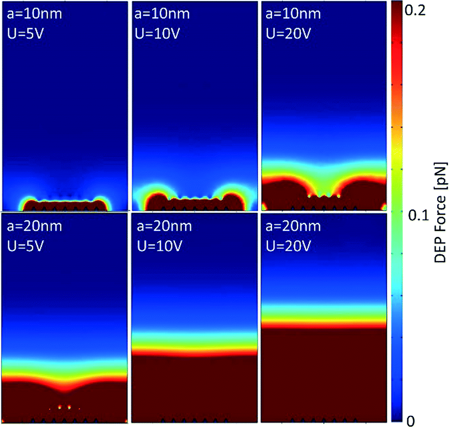 | ||
| Fig. 4 FEM simulations of the dielectric forces in the fluidic channel with nanocones implemented on the bottom electrode, acting on nanospheres with (top) radius a = 10 nm and (bottom) radius a = 20 nm. For each particle size the applied AC voltage is varied from 5 V to 10 V to 20 V. A channel height of 5 μm is simulated and plotted. The cone spacing is 250 nm. | ||
The thermal forces on the particles due to Brownian motion can be estimated as50
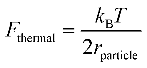 | (2) |
In the red area of Fig. 4, the dielectrophoretic forces on the nanoparticles are dominant compared to the thermal forces. It can be assumed that at least particles within this volume can be captured by the nanocones. As expected, the volume from which particles are captured is larger for the larger nanospheres and larger applied voltages. The simulation emphasizes the potential of the presented method but also shows its limitations. For particles with very small radii, this method becomes less effective because the volume from which particles are captured becomes very small. The technique could thus be combined with additional measures, such as revolving the fluid in the channel.26 Larger particles can be attracted and concentrated on the cone arrays over a distance of microns.
Results and discussion
As a proof of principle, samples with arrays of gold nanocones (25 × 25 μm2, cone height: 100 nm, cone base diameter: 120 nm) are integrated into fluidic channels as described above and used to concentrate BSA molecules on the nanocones. The channel height is varied between 2 and 20 μm, and the collection of the molecules is observed using a fluorescence microscope. After mounting the sample on the microscope stage, the BSA solution is inserted into the fluidic channel. A control image is taken, which is dark if the concentration of BSA is homogeneous and sufficiently small. Then an AC voltage (10 V, 2.5 MHz) is applied between the nanocone substrate and the channel cover. For channel heights of more than 5 μm, no accumulation of molecules is observed due to insufficient field gradients, and the fluorescence image taken after 1 minute of DEP remains dark. For a channel height of 5 μm, the simulation predicts a collection range of few 100 nm around the nanocones for small nanospheres. Here the collection of BSA on the arrays of nanocones is experimentally observed, as shown in Fig. 5. Samples with channel heights below 5 μm lead to similar results, but are experimentally more difficult to handle.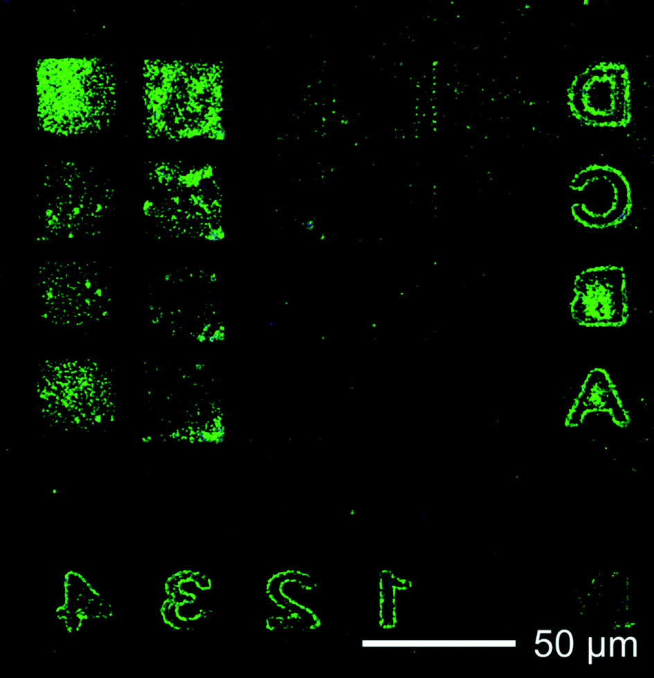 | ||
| Fig. 5 Fluorescence image (contrast enhanced) of arrays of gold nanocones in a fluidic channel after the collection of BSA molecules on the cone arrays by DEP. | ||
For the 5 μm channel, a visibly increased concentration of the fluorescently labeled BSA on the square arrays with different densities of gold nanocones is found. The four cone arrays in the left column have centre-to-centre distances of 250 nm. The following columns to the right were prepared to have centre-to-centre distances of 500 nm, 1 μm and 2 μm. In cone array D1 with a cone distance of 2 μm, the positions of the individual nanocones can be discerned through the accumulation of BSA on the cone tips. The edges of the gold markers surrounding the arrays of nanocones also exhibit strong field gradients, such that they also attract BSA molecules and appear bright in Fig. 5. This indicates that the proposed method can be performed on other shapes of plasmonic structures as well, as long as they exhibit sharp tips as the nanocones or sharp edges as the surrounding markers.
The results of this experiment successfully demonstrate the proposed method for capturing molecules down to nanometer sizes on plasmonic nanostructures. A combination of this method with sensing methods like SERS or LSPR shift sensing is expected to lead to high sensitivities and can be used to provide information with high lateral resolution.
Furthermore, the proposed method of integrating plasmonic nanostructures into a microfluidic channel could for example be combined with sorting mechanisms known from microfluidics,51,52 which could help to overcome the problem of unspecific binding of different types of molecules during the sensing procedure.
Conclusions
In conclusion, a method for capturing molecules by using plasmonic nanotips as nanoelectrodes for dielectrophoresis is developed. Gold nanocones are integrated into microfluidic channels made of SU-8 resin. By applying an AC voltage between the nanocone substrate and the cover of the channel, BSA molecules are concentrated on the cone arrays due to dielectrophoretic field gradients. The forces on particles of different sizes in the fluidic channel during the DEP process are simulated and show that the experimental dimensions are suitable for capturing nanoparticles or molecules from the vicinity of the nanocones. The proposed method is promising for a combination with subsequent optical sensing methods, in particular SERS, based on plasmonic nanostructures.Acknowledgements
The authors thank A. Heeren, C.-P. Luo, D. Gollmer, J. Fulmes, and A. Horrer for valuable discussions. This project is supported by the European Social Fund and by the Ministry of Science, Research and the Arts Baden-Wuerttemberg. Financial support from the Baden-Württemberg Foundation is gratefully acknowledged. This work was prepared in the context of the COST Action MP1302 Nanospectroscopy.Notes and references
- H. Eghlidi, K. G. Lee, X. W. Chen, S. Götzinger and V. Sandoghdar, Nano Lett., 2009, 9, 4007–4011 CrossRef CAS PubMed
.
- K. Kneipp, Y. Wang, H. Kneipp, L. T. Perelman, I. Itzkan, R. R. Dasari and M. S. Feld, Phys. Rev. Lett., 1997, 78, 1667–1670 CrossRef CAS
- M. Pfeiffer, K. Lindfors, C. Wolpert, P. Atkinson, M. Benyoucef, A. Rastelli, O. G. Schmidt, H. Giessen and M. Lippitz, Nano Lett., 2010, 10, 4555–4558 CrossRef CAS PubMed
- P. Englebienne, Analyst, 1998, 123, 1599–1603 RSC
- G. Raschke, S. Kowarik, T. Franzl, C. Soennichsen and T. A. Klar, Nano Lett., 2003, 3, 935–938 CrossRef CAS
- A. J. Haes, L. Chang, W. L. Klein and R. P. van Duyne, J. Am. Chem. Soc., 2005, 127, 2264–2271 CrossRef CAS PubMed
- X. Zhang, C. R. Yonzon, M. A. Young, D. A. Stuart and R. P. van Duyne, IEE Proc.: Nanobiotechnol., 2005, 152, 195–206 CrossRef CAS
- I.-H. Chou, M. Benford, H. T. Beier, G. L. Coté, M. Wang, N. Jing, J. Kameoka and T. A. Good, Nano Lett., 2008, 8, 1729–1735 CrossRef PubMed
- C. Wu, A. B. Khanikaev, R. Adato, N. Arju, A. A. Yanik, H. Altug and G. Shvets, Nat. Mater., 2012, 11, 69–75 CrossRef CAS PubMed
- I. Fernandez-Cuesta, A.-L. Palmarelli, X. Liang, J. Zhang, S. Dhuey, D. Olynick and S. Cabrini, J. Vac. Sci. Technol., B, 2011, 29, 06F801 Search PubMed
- S. Kumar, N. J. Wittenberg and S. H. Oh, Anal. Chem., 2013, 2, 971–977 CrossRef PubMed
- C. Xu, H. van Zalinge, J. L. Pearson, A. Glidle, J. M. Cooper, D. R. S. Cumming, W. Haiss, J. L. Yao, D. J. Schiffrin, M. Proupin-Perez, R. Cosstick and R. J. Nichols, Nanotechnology, 2006, 17, 3333–3339 CrossRef CAS PubMed
- A. Bezryadin, C. Dekker and G. Schmid, Appl. Phys. Lett., 1997, 71, 1273–1275 CrossRef CAS PubMed
- F. E. H. Tay, L. Yu and C. Iliescu, Def. Sci. J., 2009, 59, 595–604 CrossRef CAS
- A. Kuzyk, Electrophoresis, 2011, 32, 2307–2313 CAS
- S. Tuukkanen, J. J. Toppari, A. Kuzyk, P. Törmä, V. P. Hytönen and M. S. Kulomaa, Int. J. Nanotechnol., 2005, 2, 280–291 CrossRef CAS
- D. Xu, A. Subramanian, L. Dong and B. J. Nelson, IEEE Trans. Nanotechnol., 2009, 8, 449–456 CrossRef
- T. Yamamoto and T. Fujii, Nanotechnology, 2007, 18, 495503 CrossRef PubMed
- S. Tuukkanen, J. J. Toppari, A. Kuzyk, L. Hirviniemi, V. P. Hytonen, T. Ihalainen and P. Torma, Nano Lett., 2006, 6, 1339–1343 CrossRef CAS PubMed
- P. U. Arumugam, H. Chen, A. M. Cassell and J. Li, J. Phys. Chem. A, 2007, 111, 12772–12777 CrossRef CAS PubMed
- R. Löffler, M. Häffner, G. Visanescu, H. Weigand, X. Wang, D. Zhang, M. Fleischer, A. J. Meixner, J. Fortágh and D. P. Kern, Carbon, 2011, 49, 4197–4203 CrossRef PubMed
- L. Zheng, S. Li, P. J. Burke and J. P. Brody, Proc. 3rd IEEE Conf. Nanotechnol., 2003, 1, 437–440 Search PubMed.
- R. Hölzel, N. Calander, Z. Chiragwandi, M. Willander and F. F. Bier, Phys. Rev. Lett., 2005, 95, 128102 CrossRef
- R. Pethig, Biomicrofluidics, 2010, 4, 022811 CrossRef PubMed
- C. W. Marquardt, S. Blatt, F. Hennrich, H. von Löhneysen and R. Krupke, Appl. Phys. Lett., 2006, 89, 183117 CrossRef PubMed
- A. Heeren, C. P. Luo, W. Henschel, M. Fleischer and D. P. Kern, Microelectron. Eng., 2007, 84, 1706–1709 CrossRef CAS PubMed
- C. Zhang, K. Khoshmanesh, A. Mitchell and K. Kalantarzadeh, Anal. Bioanal. Chem., 2010, 396, 401–420 CrossRef CAS PubMed
- B. H. Lapizco-Encinas and M. Rito-Palomares, Electrophoresis, 2007, 28, 4521–4538 CrossRef CAS PubMed
- C. P. Luo, A. Heeren, W. Henschel and D. P. Kern, Microelectron. Eng., 2006, 83, 1634–1637 CrossRef CAS PubMed
- I.-F. Cheng, S.-H. Liao and H.-C. Changa, Biomicrofluidics, 2010, 4, 034104 CrossRef PubMed
- I.-F. Cheng, T.-Y. Chen, R.-J. Lu and H.-W. Wu, Nanoscale Res. Lett., 2014, 9, 324 CrossRef PubMed
- Y.-J. Oh and K.-H. Jeong, Lab Chip, 2014, 14, 865 RSC
- S. Cherukulappurath, S. H. Lee, A. Campos, C. L. Haynes and S.-H. Oh, Chem. Mater., 2014, 26, 2445–2452 CrossRef CAS
- L. Lesser-Rojas, P. Ebbinghaus, G. Vasan, M.-L. Chu, A. Erbe and C.-F. Chou, Nano Lett., 2014, 14, 2242–2250 CrossRef CAS PubMed
- Y.-L. Deng and Y.-J. Juang, Biomicrofluidics, 2013, 7, 014111 CrossRef PubMed
- C. Schäfer, D. A. Gollmer, A. Horrer, J. Fulmes, A. Weber-Bargioni, S. Cabrini, P. J. Schuck, D. P. Kern and M. Fleischer, Nanoscale, 2013, 5, 7861–7866 RSC
- A. Horrer, C. Schäfer, D. A. Gollmer, K. Broch, J. Rogalski, J. Fulmes, D. Zhang, A. J. Meixner, F. Schreiber, D. P. Kern and M. Fleischer, Small, 2013, 9, 3987–3992 CrossRef CAS PubMed
- F. Stade, A. Heeren, M. Fleischer and D. P. Kern, Microelectron. Eng., 2007, 84, 1589–1592 CrossRef CAS PubMed
- M. Fleischer, F. Stade, A. Heeren, M. Häffner, K. Braun, C. Stanciu, R. Ehlich, J. K. H. Hörber, A. J. Meixner and D. P. Kern, Microelectron. Eng., 2009, 86, 1219–1221 CrossRef CAS PubMed
- M. Fleischer, A. Weber-Bargioni, S. Cabrini and D. P. Kern, Microelectron. Eng., 2011, 88, 2247–2250 CrossRef CAS PubMed
- P. Reichenbach, A. Horneber, D. A. Gollmer, A. Hille, J. Mihaljevic, C. Schäfer, D. P. Kern, A. J. Meixner, D. Zhang, M. Fleischer and L. M. Eng, Opt. Express, 2014, 22, 15484–15501 CrossRef PubMed
- C. Coutal, A. Azéma and J.-C. Roustan, Thin Solid Films, 1996, 288, 248–253 CrossRef CAS
- X. Jiao, J. Goeckeritz, S. Blair and M. Oldham, Plasmonics, 2009, 4, 37–50 CrossRef CAS
- A. K. Wright and M. R. Thompson, Biophys. J., 1975, 15, 137–141 CrossRef CAS
- L. Zheng, S. Li, J. P. Brody and P. J. Burke, Langmuir, 2004, 20, 8612–8619 CrossRef CAS PubMed
- L. Zheng, P. J. Burke and J. P. Brody, Proc. SPIE, 2004, 5331, 126–135 CrossRef CAS PubMed
-
S. L. Kakani, Material Science, New Age International, 2006 Search PubMed
-
A. von Hippel, Dielectric Materials and Applications, Technology Press, 1995 Search PubMed
- L. Zheng, J. P. Brody and P. J. Burke, Biosens. Bioelectron., 2004, 20, 606–619 CrossRef CAS PubMed
- M. P. Hughes and H. Morgan, J. Phys. D: Appl. Phys., 1998, 31, 2205 CrossRef CAS
- I. Doh and Y. H. Cho, Sens. Actuators, A, 2005, 121, 59–65 CrossRef CAS PubMed
- P. Sajeesh and A. K. Sen, Microfluid. Nanofluid., 2014, 17, 1–52 CrossRef
| This journal is © The Royal Society of Chemistry 2015 |