
 Open Access Article
 This Open Access Article is licensed under a
 Creative Commons Attribution 3.0 Unported Licence
Sub-pixel resolution with a color X-ray camera
Stanisław H.
Nowak
*a,
Aniouar
Bjeoumikhov
ab,
Johannes
von Borany
c,
Josef
Buchriegler
c,
Frans
Munnik
c,
Marko
Petric
d,
Martin
Radtke
e,
Axel D.
Renno
f,
Uwe
Reinholz
e,
Oliver
Scharf
a and
Reiner
Wedell
g
aIfG – Institute for Scientific Instruments GmbH, Berlin, Germany. E-mail: nowak@ifg-adlershof.de
bInstitute for Computer Science and Problems of Regional Management, Kabardino-Balkaria, Russia
cHelmholtz-Zentrum Dresden-Rossendorf, Dresden, Germany
dJ. Stefan Institute, Ljubljana, Slovenia
eBAM Federal Institute for Material Research and Testing, Berlin, Germany
fHelmholtz-Zentrum Dresden-Rossendorf, Helmholtz Institute Freiberg for Resource Technology, Freiberg, Germany
gIAP Institute for Applied Photonics e.V., Berlin, Germany
First published on 1st June 2015
Abstract
The color X-ray camera SLcam® is a full-field, single photon detector providing scanning-free, energy and spatially resolved X-ray imaging. Spatial resolution is achieved with the use of polycapillary optics guiding X-ray photons from small regions on a sample to distinct energy dispersive pixels on a charged-coupled device detector. Applying sub-pixel resolution, signals from individual capillary channels can be distinguished. Therefore, the SLcam® spatial resolution, which is normally limited to the pixel size of the charge-coupled device, can be improved to the size of individual polycapillary channels. In this work a new approach to a sub-pixel resolution algorithm comprising photon events also from the pixel centers is proposed. The details of the employed numerical method and several sub-pixel resolution examples are presented and discussed.
1 Introduction
The SLcam® is a high quantum efficiency and throughput color X-ray camera system1–3 designed for divergent X-ray radiation sources. It allows the detection of single photons with both energy and spatial resolution. This detector combines a pn-junction Charged-Coupled Device (pnCCD)4 with a polycapillary optic.5 The latter can be regarded as a bunch of independent X-ray channels guiding X-ray photons from small regions on a sample to corresponding pixels on the pnCCD similarly to the way fiber optic guides light.The SLcam® employs a pnCCD with 48 μm pixel size. While keeping the pixel size fixed the spatial resolution of the color camera can be seriously improved by the use of a conically shaped magnifying optic.2,3 This type of optic is available with magnification factors up to 10![[thin space (1/6-em)]](https://www.rsc.org/images/entities/char_2009.gif) :1, allowing the representation of a ∼5 × 5 μm2 area in a single pixel. Theoretically, according to the Nyquist–Shannon sampling theorem,6 such a system can correctly resolve details above ∼10 μm. Be advised, however, that magnification is achieved at the cost of a reduced field of view.
:1, allowing the representation of a ∼5 × 5 μm2 area in a single pixel. Theoretically, according to the Nyquist–Shannon sampling theorem,6 such a system can correctly resolve details above ∼10 μm. Be advised, however, that magnification is achieved at the cost of a reduced field of view.
The presently used SLcam® optics are optimized for the pnCCD pixel dimension and the pixel size is the limiting factor for the spatial resolution of the camera. The capillary exit diameter is adapted in such a way that the spot size from an individual channel on the detector is close to the pixel size. The resulting diameter of single capillary channels is around 20 μm. However, current technology allows the fabrication of polycapillaries with a channel diameter in the range of a micron or even below. This gives room for further improvement of the resolution.
By using a sub-pixel algorithm the dominant role of the pixel size can be released. This algorithm divides the signal assigned to each physical pixel over a number of virtual sub-pixels while not affecting the physical area which can be imaged. With such an approach further downscaling of polycapillary channels can be practically used for the improvement of the SLcam® lateral resolution.
Images with sub-pixel resolution are achievable due to the specific physics of the interaction of an X-ray photon within the Charged-Coupled Device (CCD) that leads to the creation of a so-called electron cloud. A non-zero area of this cloud leads to charge deposition in pixels nearest to the photon hit. With a correct reconstruction of the footprint of a single photon event the photon hit position can be estimated. A precision much higher than the pixel size can be achieved.
The sub-pixel resolution algorithm was first applied to the Advanced CCD Imaging Spectrometer (ACIS) installed at the Chandra X-ray Observatory (CXO).7–12 Some years later, a similar technique was adapted to the pnCCD.13,14 Unfortunately, the proposed routines are neglecting the majority of events analyzing only so-called “corner events”, i.e., the photon hits that reach the CCD in proximity to a pixel corner. As a result the sub-pixel image exhibits a grid pattern with a drop of intensity in the pixel centers.3 We propose a modified approach taking all the photon hits and distributing them properly over the sub-pixel pattern.
2 Method
2.1 Electron cloud
An X-ray photon absorbed in silicon generates a number of electron–hole pairs amounting to E/WSi – the photon energy E divided by the formation energy of a single electron–hole pair WSi = 3.6 eV.15 In a fully depleted layer the carriers are separated in the vertical electric field and diffuse laterally producing two charge clouds with opposite signs. The holes are collected at the large area cathode. The electrons are transferred to the pixelated anode where they are split over individual pixels. During the readout these charge packets are sequentially transferred to charge amplifiers and counted.The carrier density of a single photon electron cloud is frequently approximated by a two dimensional Gaussian distribution:11,16–18
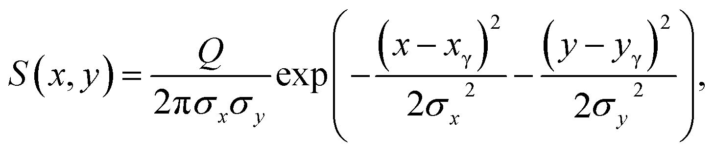 | (1) |
 | (2) |
Though this is a simplified model neglecting the energy dependence, charge quantization, etc., it shows the fundamental fact making the sub-pixel resolution algorithm possible: on a pixelated plane a single photon electron cloud is normally split over several pixels. For every photon hit, in addition to the pixel position, extra information in the form of a pixel intensity distribution is gathered. This additional information can be used to determine the center of impact of the photon with sub-pixel accuracy.
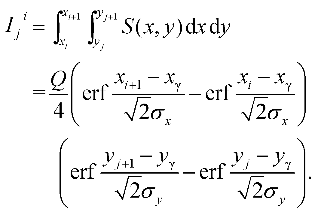
2.2 Intensity ratios
A good measure of the electron cloud distribution of a single photon is the intensity ratio defined as follows: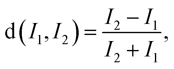 | (3) |
It can be shown that for any electron cloud distribution for which the x and y components can be separated (e.g. a Gaussian distribution) the pixel intensity ratio in the x direction is independent from the y coordinate and vice versa:
| d(Iji−1, Iji) = d(Iki−1, Iki), | (4) |
| d(Ij−1i, Iji) = d(Ij−1l, Ijl). | (5) |
A very elegant way to estimate the electron cloud distribution of a single photon was presented in ref. 19. The method relies on the analysis of a histogram of measured intensity ratios and assumes only a uniform distribution of photon hits over the CCD plane and a Gaussian shape of the charge cloud. The method was used to reveal the size of the cloud. We will use a similar methodology to calculate sub-pixel coordinates.
In order to calculate the intensity ratio histogram 2 × 2 pixel boxes centered at the pixel corner (xi, yj) nearest to the point of a photon hit (xγ, yγ) are analyzed. Intensity ratios in x and y directions, respectively, are calculated as follows:
| dx = d(Ij−1i−1 + Iji−1, Ij−1i + Iji) | (6) |
| dy = d(Ij−1i−1 + Ij−1i, Iji−1 + Iji). | (7) |
The intensity ratios in the x or y direction computed for all single photon hits are combined in one histogram.
The histogram normalized to occupy a unitary area can be regarded as an estimation of the probability density function. Accordingly, such a histogram rates the probability of a single photon hit to create a given intensity ratio value.
In Fig. 1 an example of a normalized intensity ratio histogram is plotted. The figure shows data computed for Au L photons from the measurement of an Au bar pattern presented further in Section 3. As can be seen most of the photon hits create electron clouds with an intensity ratio in the proximity of −1 or 1. Intensity ratios close to 0 are the least probable. The discussed Gaussian model fits well to most values of the histogram; though for |dx| ≈ 1 (and |dy| ≈ 1) the simulation fails showing a deficiency of the model.
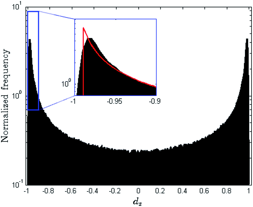 | ||
| Fig. 1 An example of an intensity ratio histogram for Au L photons generated from a real measurement (Au bar pattern, see Section 3) with formula (6). The histogram is normalized to occupy a unitary area and can be identified with the probability density function. In the inset the histogram is compared to a Gaussian simulation (red line). | ||
2.3 Sub-pixel coordinates
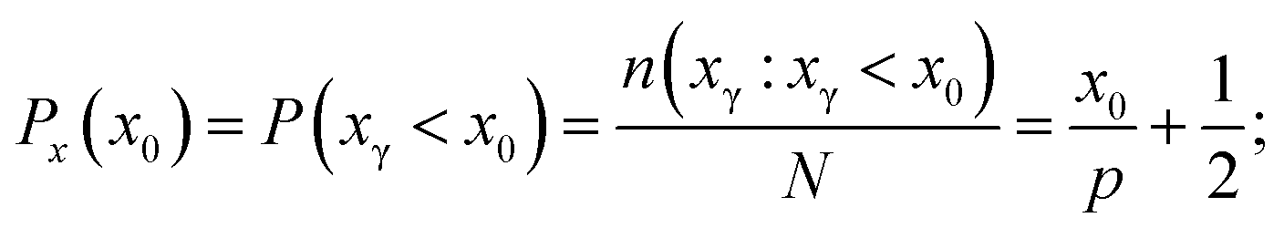
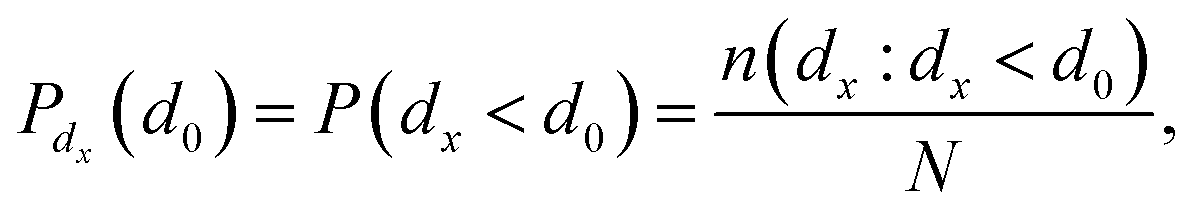
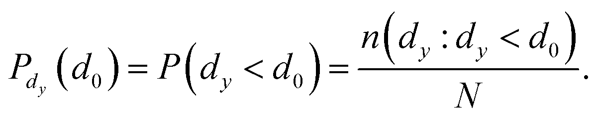
Our method consists in converting the dx and dy intensity ratios of a given photon hit to xγ and yγ coordinates. In our approach we do not model the shape of the single photon electron cloud; we assume only the separation of the x and y components of the charge distribution. We also assume a uniform distribution of photon hits over the CCD plane. Accordingly the relation between the intensity ratio and the position of a single photon hit is not simulated, but measured.Let us set (xi, yj) – the pixel corner nearest to the point of a photon hit – to the origin, and the number of photon events to N. The possible values for xγ inside a 2 × 2 pixel box span the range 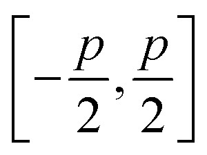 , where p is the pixel dimension. Due to the uniform distribution of the photon hit positions over the CCD plane the probability of finding a photon hit with the xγ coordinate below x0 has a linear form:
 | (8) |
 | (9) |
 | (10) |
| n(xγ:xγ < x0) = n(dx:dx < dx(x0)). | (11) |
| Px(xγ) = Pdx(dx(xγ)). | (12) |
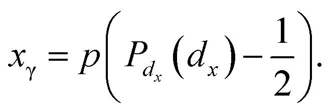 | (13) |
The relationship between xγ, dx and Pdx is shown in Fig. 2.
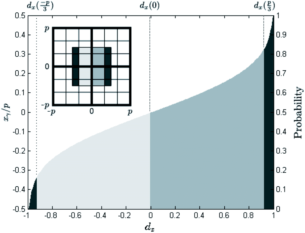 | ||
| Fig. 2 The relative photon hit position xγ calculated as a function of the intensity ratio dx according to eqn (13). Like in Fig. 1 the data for Au L photons from the Au bar pattern are illustrated. The secondary vertical axis shows the cumulative probability distribution Pdx. In the inset a 2 × 2 pixel box with a 3 × 3 sub-pixel division is shown. Different levels of gray mark – in order from darkest to brightest – central, left and right sub-pixels. | ||
2.4 Division into sub-pixels
The cloud creation process and the resulting charge distribution is a physical process that should not change in time. Therefore each measurement could be analyzed with the use of a single set of previously obtained pixel intensity ratio probabilities. In order to minimize the statistical error Pdx and Pdy should be generated in a measurement with good statistics of single photon hits.A strong point of our method is that it is independent from the shape and creation process of the electron cloud and can deal with any, also asymmetric,9 charge distributions. In an ideal case of uniformly shaped electron clouds and a hypothetical noise-free CCD, eqn (13) should give a strict position of a single photon hit.
In reality the electron cloud is shaped randomly and the intensity signal from each pixel is given with an error. These two factors contradict the assumptions on the monotonic relation between dx and xγ and on the separation of the x and y components. As a result the accuracy of the sub-pixel coordinates is limited.
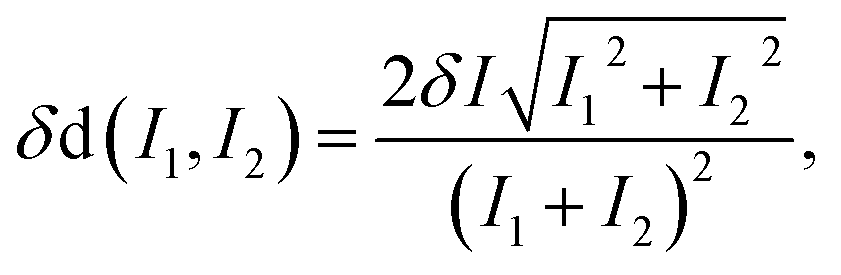
We can estimate an error for d(I1, I2) with the following relation:
 | (14) |
 . This is exactly where Pdx exhibits the largest increase and, respectively, where the error on Pdx is biggest.
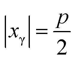
As a result the photon hit position is most inaccurate in proximity to the pixel center  . In order to minimize that effect the sub-pixel division should comprise that higher uncertainty central region in a single sub-pixel. An exemplary division into 3 sub-pixels in the x direction is shown in Fig. 2.
In conclusion, the assignment of sub-pixel coordinates to a given photon event consist only of two steps: (i) calculation of dx and dy with formulas (6) and (7), and (ii) comparison of the obtained values with sub-pixel borders expressed in pixel ratio coordinates. These are simple arithmetic operations that can be readily computed. As a result the algorithm is fast and can be applied in real-time with only a little increase in processing overhead for data acquisition.
3 Experimental
Fig. 3 shows sketches of two test samples that were measured to examine the performance of the sub-pixel algorithm. The first one contains a layer of Au on a Si support arranged in bar-like patterns and a uniform reference layer.20 The bar pattern consists of 10 Au lines with the width and the spacing between them increasing from 1 μm to 10 μm in 1 μm steps. The resolution limit can easily be found as the width of the narrowest recognizable line. The second structure was produced by the Fraunhofer-Institut für Zuverlässigkeit und Mikrointegration (IZM) and consists of 3 μm thick and 30 μm wide Cu stripes deposited on a Si wafer with a 200 nm TiW adhesion layer. The stripes are aligned in parallel and distributed in groups with constant spacing of 30, 60 and 90 μm. In addition to the test structures an exemplary geological sample was measured. The sample is a molybdenum ore (or Mo-ore) from the copper–molybdenum mine in Kajaran (Armenia) and it is kindly provided by the Geoscientific Collections of the TU Bergakademie Freiberg.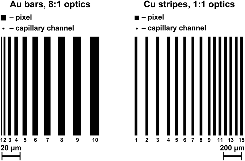 | ||
| Fig. 3 Sketches of an Au bar pattern (left) and Cu stripes (right), and corresponding sizes of a pixel (side length of 6 and 48 μm, respectively) and a capillary channel (entrance diameter of 2 and 20 μm, respectively). The structures' elements are numbered for ease of reference. Note the different scale of the left and right panels. | ||
Imaging was performed with two types of polycapillary lenses – a high-resolution conical optic with an 8:1 magnification that was employed for the Au pattern, and a parallel 1:1 optic used for the Cu stripes structure and the Mo-ore. The magnification optic has a single channel entrance diameter of din = 2 μm. The exit diameter of a channel span to dout = 16 μm which is one third of the pixel size (p = 48 μm). The single channel diameter of the 1:1 optic amounts to d = 20 μm, which is almost half the pixel size.
In order to ensure a high enough photon count rate, measurements were performed at the synchrotron radiation facility BESSY II with the beam provided by the BAMline,21 and at the newly developed PIXE beam line (High-Speed PIXE) at the Ion Beam Center of the Helmholtz-Zentrum Dresden-Rossendorf (HZDR).22 Detailed descriptions of the two setups can be found in ref. 3 and 22.
For imaging purposes intensity distributions of several characteristic X-ray lines were assessed. Valid photon events were selected with an algorithm described elsewhere.3 The algorithm rejects noise and events such as cosmic rays and accepts only photon events having an appropriate arrangement of pixels above the noise threshold.
The position of the photon hit is first estimated by the weighted position of the pixel with the highest intensity and its nearest neighbours. Subsequently a 2 × 2 pixel box around a pixel corner closest to the estimated position is selected and the sub-pixel algorithm is applied. The probability functions of pixel intensity ratios in x and y directions were obtained directly from the measurements. Probability density and the cumulative probability functions of the intensity ratios in the x direction for Au L photons are presented in Fig. 1 and 2.
4 Results
4.1 Au bar pattern
In Fig. 4 the image of the Au bar pattern is presented in normal resolution and with pixels divided to 2 × 2 and 3 × 3 sub-pixels. The normal resolution image exhibits strong pixelation introducing artificial jerking of the Au bars and decreasing the contrast between structure and background. Only the 4 thickest stripes can be distinguished in the original image; the rest is blurred. With the division into 2 × 2 sub-pixels another Au line is resolved. The 3 × 3 sub-pixel division, however, does not introduce any visible improvement. In this regime a single sub-pixel corresponds to a distance of 2 μm on the sample which is exactly the entrance channel diameter of the polycapillary optic (2 μm). In addition, the small effective area of a sub-pixel significantly lowers the count rate and increases the noise contribution.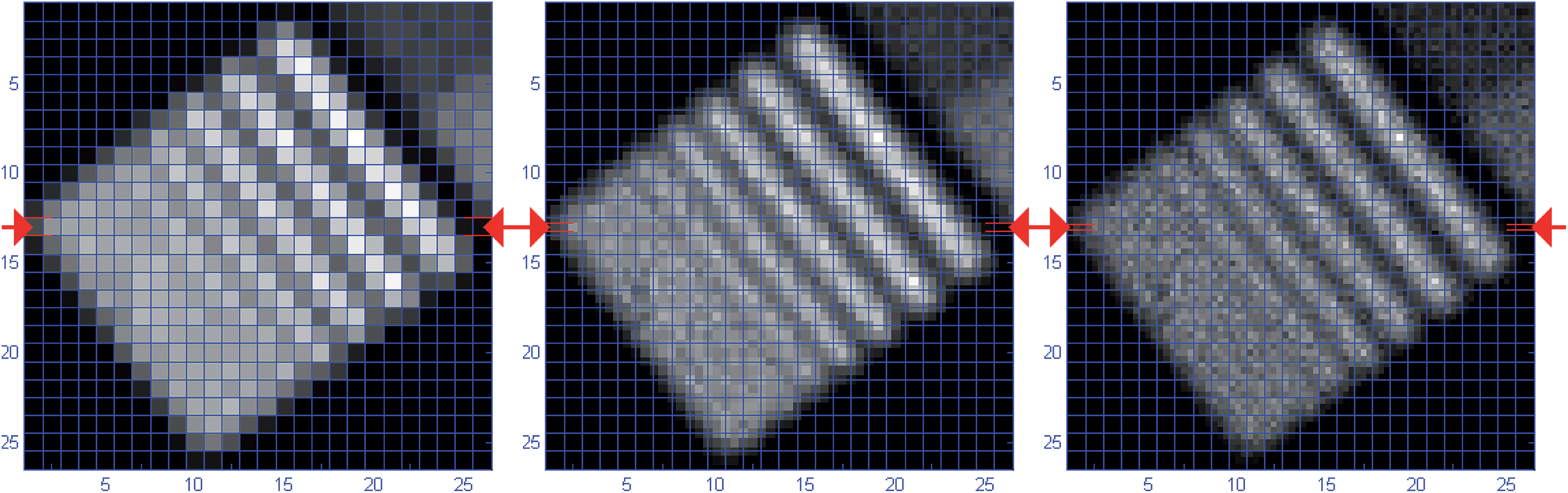 | ||
| Fig. 4 Images with normal resolution (left), 2 × 2 (center) and 3 × 3 (right) sub-pixel division of the Au bar pattern. The image was acquired at the BAMline at BESSY II with an 8:1 magnification lens. The grid shows the positions of the real pixels, each corresponding to a 6 × 6 μm2 area on the sample surface. Red arrows indicate the (sub-)pixel row chosen for comparison in Fig. 5. | ||
In Fig. 5 three intensity profiles along a single (sub-)pixel row are depicted. A drop of intensity with pixel division is clearly visible. This is an effect of the decrease of the sub-pixel area. For a pixel divided into n × n sub-pixels the intensity is decreased n2 times. However, the increased sampling frequency evidently increases the contrast. For the profile with no sub-pixel division only the 4 thickest Au bars can be definitely differentiated. The intensity valley between the 6 μm and 5 μm bars is not visible. In the case of 2 × 2 pixel division the 6 μm bar can be clearly distinguished. For the 3 × 3 sub-pixel division there is no significant amendment due to the considerable noise content.
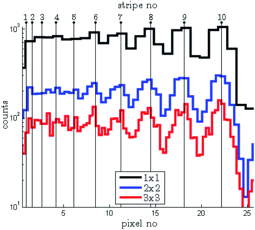 | ||
| Fig. 5 Pixel intensity profiles along one sub-pixel row indicated in Fig. 4 with the red arrows. The profiles are plotted for normal resolution (black line), 2 × 2 (blue line), and 3 × 3 (red line) sub-pixel division. The estimated positions of the Au bar centers are indicated with black vertical lines. | ||
It should be noted that due to the Nyquist–Shannon sampling theorem,6 details smaller than twice the sampling distance cannot be correctly distinguished. The theorem says that making n samples over a certain distance only a signal comprising less than n/2 elements can be rendered properly. A higher number of elements will lead to signal aliasing resulting in distortions and artifacts. With the sub-pixel division an improvement can be achieved by the deliberate increase of the sampling frequency.
As a single pixel in an 8:1 magnified image represents a square with a side length of 6 μm, the camera in standard resolution cannot correctly represent features smaller than 12 μm. Still, as can be seen in the presented example, even without sub-pixel resolution much smaller lines can be distinguished, though with some alterations. For instance in Fig. 5 the normal resolution profile shows the 8 μm bar to be thicker than the 9 μm one.
In Fig. 6 two additional intensity profiles are shown. The profiles represent the cumulative intensity sampled independently from the pixel layout across lines parallel to the Au bars. The sampling interval is identical for both curves corresponding to normal resolution and 3 × 3 sub-pixel division; therefore the relative intensity of two profiles does not differ. For the sake of legibility the profile corresponding to a 2 × 2 sub-pixel division is not present.
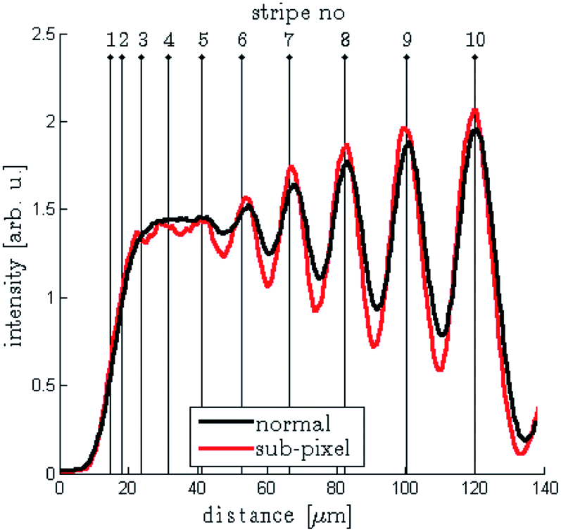 | ||
| Fig. 6 Intensity profile across the Au bar structures calculated for normal resolution (black line) and 3 × 3 sub-pixel division (red line). The estimated positions of the Au bar centers are indicated with black vertical lines. The intensity profiles were constructed from images presented in Fig. 4. The data was resampled at regular intervals perpendicular to the Au bars. To increase the signal to noise ratio the intensity was integrated over the whole length of the Au bars. | ||
The tilt of the sampling direction with respect to the pixel lines eliminates the effects due to pixelation. As a consequence the 6 μm Au bar can be resolved even in the case of normal resolution. Also here the contrast improves when sub-pixel resolution is applied. In addition the enlarged integration area increases the statistics reducing the noise contribution. As a result the sub-pixel resolution profile allows the distinction of 5 μm or even 4 μm bars.
4.2 Cu stripes
The consequences of too sparse sampling are clearly visible in the image of the Cu stripes (see Fig. 7). The image represents a structure with three groups of Cu stripes with dimensions below the Nyquist–Shannon resolution limit. Here the structure is aligned with the pixels and the effect of aliasing is clearly visible. Images with normal resolution and 3 × 3 sub-pixel division are presented for comparison.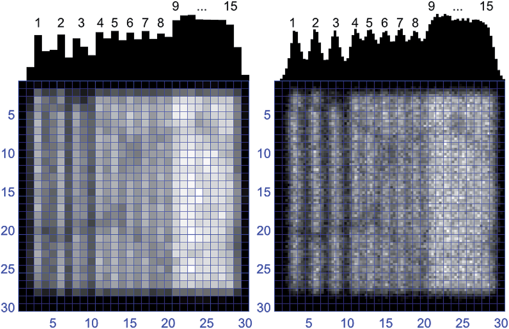 | ||
| Fig. 7 Images with normal resolution (left) and 3 × 3 sub-pixel resolution (right) of the Cu stripes pattern. The image was acquired at the HS-PIXE beam line at HZDR with a parallel 1:1 optic. The grid shows the positions of the real pixels, each corresponding to 48 × 48 μm2 area on the sample surface. On top the cumulative intensity along each (sub-)pixel column is presented. The Cu stripes are numbered for ease of reference. | ||
The group on the left (stripes 1 to 3) has an interval (120 μm) large enough to fulfill the Nyquist–Shannon theorem, but individual stripe widths are too small. Therefore the structure is clearly resolved, however the stripe widths and positions are not rendered well giving a false impression of a patchy structure. The sub-pixel resolution image correctly presents uniform, equidistant stripes.
The central group (stripes from 4 to 8) is distributed with an interval of 90 μm. This is comparable to the Nyquist–Shannon resolution limit, i.e., double the pixel size (p = 48 μm). In the standard image the stripes are merely distinguishable and confined to a single pixel line. The sub-pixel resolution image shows a more legible representation of the structure with the single stripe signal distributed over several sub-pixels.
In Table 1 the actual dimensions of the line widths in these two groups are compared with the standard resolution and the sub-pixel measured values. It should be noticed that the sub-pixel results have a much lower spread and are much closer to the real data. In the case of standard resolution the effect of aliasing can be seen in the stripes' lengths which are confined to a multiple of the pixel width (48 μm).
| Line no. | 1 | 2 | 3 | 4 | 5 | 6 | 7 | 8 | ||||||||
|---|---|---|---|---|---|---|---|---|---|---|---|---|---|---|---|---|
| a Pixel size [μm]: 48, capillary channel [μm]: 20. | ||||||||||||||||
| Width [μm] | Nominal | 30 | 30 | 30 | 30 | 30 | 30 | 30 | 30 | |||||||
| 1 × 1 | 48 | 48 | 96 | 48 | 48 | 48 | 48 | 48 | ||||||||
| 3 × 3 | 37 | 36 | 35 | 41 | 42 | 44 | 46 | 54 | ||||||||
| Interval [μm] | Nominal | 120 | 120 | 120 | 90 | 90 | 90 | 90 | ||||||||
| 1 × 1 | 144 | 96 | 144 | 96 | 96 | 96 | 96 | |||||||||
| 3 × 3 | 129 | 120 | 124 | 96 | 91 | 96 | 96 |
For both the central and left groups there is a noticeable increase of the contrast level when sub-pixel resolution is used. The contrast in the central group is much smaller when compared to the left most group. This is not surprising as the structure dimensions are much closer to the size of a single polycapillary channel which is the ultimate resolution limit of the optic.
Finally, the right most group (stripes 9 to 15) is too confined and individual stripes cannot be distinguished even when sub-pixel resolution is applied. Here the structure has stripes with dimensions and spacing of 30 μm which is too close to the single capillary channel diameter (20 μm).
4.3 Au layer
As stated in Section 2.4 the maximal number of sub-pixel divisions is restricted. In order to find a limiting number of sub-pixels an additional assay was performed on a reference uniform Au layer. A small portion of the image was compared for the case of normal pixel resolution and increasing sub-pixel divisions.As can be seen in Fig. 8 the increased number of sub-pixels gives rise to statistical noise. This was expected as the counts per sub-pixel are reduced. In addition, for very dense divisions, the creation of intensity artifacts following the position of the pixel center can be seen (see the 9 × 9 sub-pixel division in Fig. 8). This effect was already discussed in Section 2.4 and is the result of the position uncertainty of a photon hit reaching the middle area of a pixel. Nevertheless, pixel divisions up to 5 × 5 sub-pixels are usually not affected by this inconvenience.
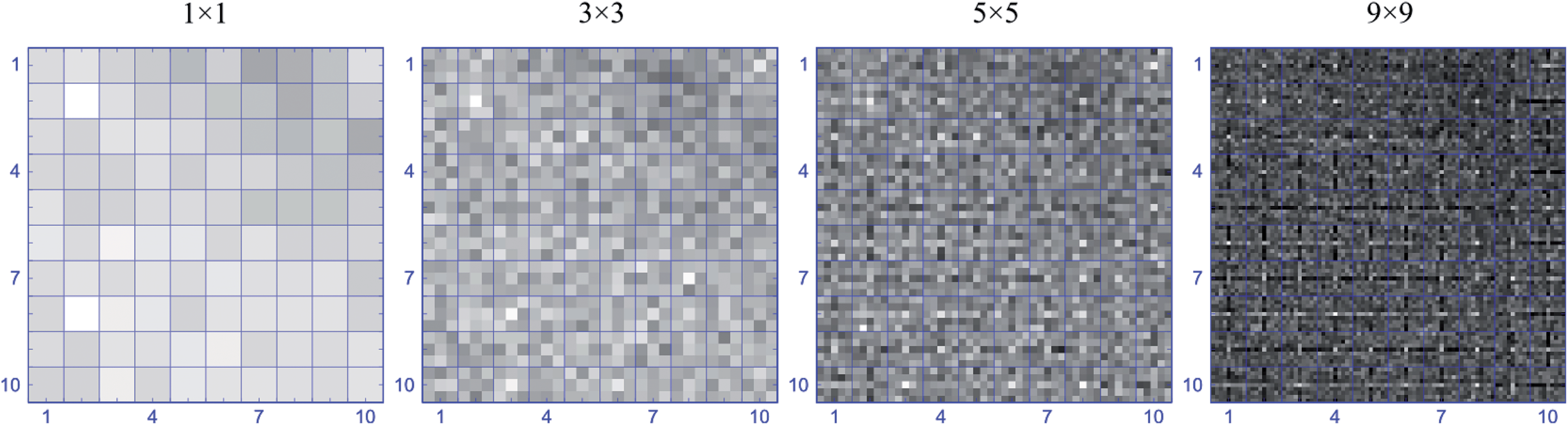 | ||
| Fig. 8 Images with normal resolution and 3 × 3, 5 × 5, and 9 × 9 sub-pixel division of a 60 × 60 μm2 piece of Au layer. The image was acquired at the BAMline at BESSY II with an 8:1 magnification lens. The increase of statistical noise and the appearance of intensity artifacts following the pixel center position are visible for the sub-pixel resolution images. The grid in blue shows the real pixel positions. | ||
Keeping in mind that the dimension of a pnCCD pixel is 48 μm, a pixel division into 5 × 5 sub-pixels results in a sub-pixel of 9.6 μm side length. At the same time the nonzero divergence of the polycapillary optic and a nonzero distance between the optic and the pnCCD restricts the footprint of a single polycapillary channel on the detector to at least a dozen of microns. Therefore, sub-pixel division up to 5 × 5 should be sufficient to reach the optimal limits of the SLcam® resolution.
4.4 Molybdenum ore
An exemplary geological sample was measured with the 1:1 polycapillary optic at the High-Speed PIXE beamline at HZDR. The false color image presented in Fig. 9 was obtained by superposing color maps corresponding to the intensity of characteristic fluorescence lines of several elements. The main image was rendered in 3 × 3 sub-pixel resolution. In the insets smaller details of the image are compared for standard and sub-pixel resolution.
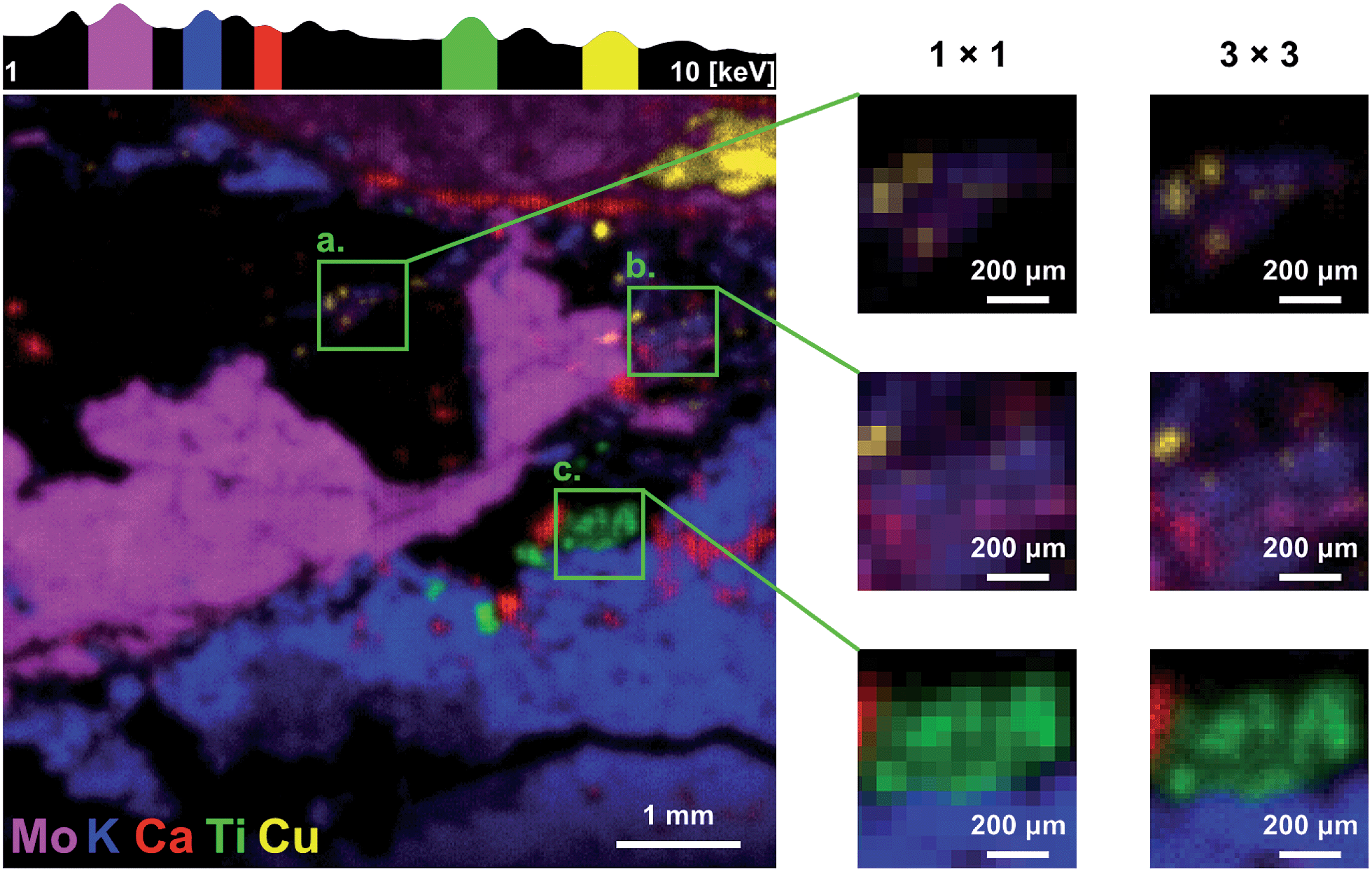 | ||
| Fig. 9 Image of a molybdenum ore measured at the High-Speed PIXE beamline at HZDR with the 1:1 polycapillary optic. Different colors are assigned to the intensity of, respectively, Mo Lα, K Kα, Ca Kβ, Ti Kα, and Cu Kα fluorescence lines. The main image is displayed with 3 × 3 sub-pixel resolution. On top a logarithmic representation of the sum spectrum of the full-image area is presented. Small panels on the right side of the image represent ×2.5 magnified image details in standard and 3 × 3 sub-pixel resolution. | ||
With the sub-pixel resolution it is possible to resolve small grains that overlap in standard resolution (see inset a). Spots with dimensions corresponding to the pixel size (48 μm) are clearly recognizable. The contrast of the sub-pixel image is enhanced and the effects of pixelation are reduced for both multi and single element images (see insets b. and c.). As a result different grains and intergrowth areas can be identified with much better precision.
5 Summary and outlook
We propose a modified approach to a sub-pixel resolution algorithm taking into account all the valid photon events occurring on a CCD plane. The sub-pixel position of the photon hit is assessed from the pixel footprint of the generated electron cloud. The calculations are performed based on the pixel intensity ratios of a 2 × 2 pixel box holding photo electrons. The method is independent from the actual shape and creation process of the charge cloud and does not reject the photon events from the pixel center. The sub-pixel algorithm does not influence the physical size of the image; it increases the number of (sub-)pixels per unit length instead. However, the number of photon counts per sub-pixel is reduced since the counts in a single pixel are divided.The sub-pixel resolution was applied to several test structures and an exemplary geological sample. A notable enhancement in quality of the acquired images comprising an improvement of contrast and resolution, as well as the elimination of pixel aliasing was demonstrated. For images acquired with the 8:1 magnifying optic a resolution limit of 5 μm was assessed. Due to electronic noise and random variations of the electron cloud shape the sub-pixel coordinates cannot be given with unlimited precision. It was shown that in the case of a 48 × 48 μm2 pixel pnCCD the 5 × 5 sub-pixel division is a realistic limit of the method.
The algorithm is fast, does not require any hardware changes, and can be employed in real time. Sub-pixel post-processing is also possible if measurements are saved in an event file data format. The SLcam® control software is currently developed to include the sub-pixel routine to make it easily available to the users.
Acknowledgements
This work has been supported by Marie Curie Actions – Initial Training Networks (ITN) as an Integrating Activity Supporting Postgraduate Research with Internships in Industry and Training Excellence (SPRITE) under EC contract no. 317169.References
- A. Kühn, O. Scharf, I. Ordavo, H. Riesemeier, U. Reinholz, M. Radtke, A. Berger, M. Ostermann and U. Panne, J. Anal. At. Spectrom., 2011, 26, 1986–1989 RSC.
- I. Ordavo, S. Ihle, V. Arkadiev, O. Scharf, H. Soltau, A. Bjeoumikhov, S. Bjeoumikhova, G. Buzanich, R. Gubzhokov, A. Günther, R. Hartmann, P. Holl, N. Kimmel, M. Kühbacher, M. Lang, N. Langhoff, A. Liebel, M. Radtke, U. Reinholz, H. Riesemeier, G. Schaller, F. Schopper, L. Strüder, C. Thamm and R. Wedell, Nucl. Instrum. Methods Phys. Res., Sect. A, 2011, 654, 250–257 CrossRef CAS PubMed.
- O. Scharf, S. Ihle, I. Ordavo, V. Arkadiev, A. Bjeoumikhov, S. Bjeoumikhova, G. Buzanich, R. Gubzhokov, A. Günther, R. Hartmann, M. Kühbacher, M. Lang, N. Langhoff, A. Liebel, M. Radtke, U. Reinholz, H. Riesemeier, H. Soltau, L. Strüder, A. F. Thünemann and R. Wedell, Anal. Chem., 2011, 83, 2532–2538 CrossRef CAS PubMed.
- L. Strüder, U. Briel, K. Dennerl, R. Hartmann, E. Kendziorra, N. Meidinger, E. Pfeffermann, C. Reppin, B. Aschenbach, W. Bornemann, H. Bräuninger, W. Burkert, M. Elender, M. Freyberg, F. Haberl, G. Hartner, F. Heuschmann, H. Hippmann, E. Kastelic, S. Kemmer, G. Kettenring, W. Kink, N. Krause, S. Müller, A. Oppitz, W. Pietsch, M. Popp, P. Predehl, A. Read, K. H. Stephan, D. Stötter, J. Trümper, P. Holl, J. Kemmer, H. Soltau, R. Stötter, U. Weber, U. Weichert, C. V. Zanthier, D. Carathanassis, G. Lutz, R. H. Richter, P. Solc, H. Böttcher, M. Kuster, R. Staubert, A. Abbey, A. Holland, M. Turner, M. Balasini, G. F. Bignami, N. L. Palombara, G. Villa, W. Buttler, F. Gianini, R. Lainé, D. Lumb and P. Dhez, Astron. Astrophys., 2001, 365, 18–26 CrossRef.
- A. Bjeoumikhov, N. Langhoff, R. Wedell, V. Beloglazov, N. Lebed'ev and N. Skibina, X-Ray Spectrom., 2003, 32, 172–178 CrossRef CAS PubMed.
- C. E. Shannon, Proc. IRE, 1949, 37, 10–21 CrossRef.
- H. Tsunemi, K. Yoshita and S. Kitamoto, Jpn. J. Appl. Phys., 1997, 36, 2906–2911 CrossRef CAS.
- M. Pivovaroff, S. Jones, M. Bautz, S. Kissel, G. Prigozhin, G. Ricker, H. Tsunemi and E. Miyata, IEEE T. Nucl. Sci., 1998, 45, 164–175 CrossRef CAS.
- H. Tsunemi, J. Hiraga, K. Yoshita and E. Miyata, Jpn. J. Appl. Phys., 1999, 38, 2953–2957 CrossRef CAS.
- K. Yoshita, H. Tsunemi, E. Miyata, K. Gendreau and M. Bautz, IEEE Trans. Nucl. Sci., 1999, 46, 100–106 CrossRef.
- J. Hiraga, H. Tsunemi and E. Miyata, Jpn. J. Appl. Phys., 2001, 40, 1493–1498 CrossRef CAS.
- J. Li, J. H. Kastner, G. Y. Prigozhin and N. S. Schulz, Astrophys. J., 2003, 590, 586–592 CrossRef PubMed.
- N. Kimmel, J. S. Hiraga, R. Hartmann, N. Meidinger and L. Strüder, Nucl. Instrum. Methods Phys. Res., Sect. A, 2006, 568, 128–133 CrossRef CAS PubMed.
- A. Abboud, S. Send, N. Pashniak, W. Leitenberger, S. Ihle, M. Huth, R. Hartmann, L. Strüder and U. Pietsch, J. Instrum., 2013, 8, P05005 Search PubMed.
- F. Scholze, H. Rabus and G. Ulm, J. Appl. Phys., 1998, 84, 2926–2939 CrossRef CAS PubMed.
- J. R. Janesick, Scientific Charge-Coupled Devices, SPIE Publications (SPIE Press Monograph), vol. PM83, 2001 Search PubMed.
- G. R. Hopkinson, Opt. Eng., 1987, 26, 268766 CrossRef PubMed.
- E. Miyata, M. Miki, D. Kamiyama, H. Tsunemi and K. Miyaguchi, Jpn. J. Appl. Phys., 2003, 42, 7135–7139 CrossRef CAS.
- D. Lawrence, P. O'Connor, J. Frank and P. Takacs, Publ. Astron. Soc. Pac., 2011, 123, 1100–1106 CrossRef.
- E. Strub, M. Radtke, U. Reinholz, H. Riesemeier and E. Reznikova, Nucl. Instrum. Methods Phys. Res., Sect. B, 2008, 266, 2165–2168 CrossRef CAS PubMed.
- H. Riesemeier, K. Ecker, W. Görner, B. Müller, M. Radtke and M. Krumrey, X-Ray Spectrom., 2005, 34, 160–163 CrossRef CAS PubMed.
- S. H. Nowak, A. Bjeoumikhov, J. von Borany, J. Buchriegler, F. Munnik, M. Petric, A. D. Renno, M. Radtke, U. Reinholz, O. Scharf, L. Strüder, R. Wedell and R. Ziegenrücker, X-Ray Spectrom., 2015, 44, 135–140 CrossRef CAS PubMed.
| This journal is © The Royal Society of Chemistry 2015 |