
Capabilities and limitations of LA-ICP-MS for depth resolved analysis of CdTe photovoltaic devices†
Ana
Gutiérrez-González
a,
Cristina
González-Gago
a,
Jorge
Pisonero
*a,
Nicole
Tibbetts
b,
Armando
Menéndez
c,
María
Vélez
a and
Nerea
Bordel
a
aDepartment of Physics, University of Oviedo, Mieres, Oviedo, Spain. E-mail: pisonerojorge@uniovi.es
bGeneral Electric Global Research, Niskayuna, USA
cEnergy Area (EN) – ITMA Materials Technology (Fundación ITMA), Avilés, Spain
First published on 13th August 2014
Abstract
The analytical potential of ArF* excimer Laser Ablation Inductively Coupled Plasma Mass Spectrometry (LA-ICP-MS) is investigated for fast qualitative depth profile analysis of multi-layer CdTe photovoltaic (PV) devices. Critical parameters (e.g. laser fluence and laser repetition rate) are evaluated and optimized to reduce the aerosol mixing from consecutive laser shots and to achieve a low penetration rate. As a result, a high depth resolution (10 s of nm) is demonstrated through the analyses of superficial and embedded coatings. For instance, a layer with a thickness of 100 nm at a depth of 3 μm is successfully measured. Moreover, qualitative profiles of major and minor elements obtained by LA-ICP-MS are validated using reference techniques such as Secondary Ion Mass Spectrometry (SIMS) or Glow Discharge Time of Flight Mass Spectrometry (GD-TOFMS). Additionally, the shape and morphology of the laser-induced craters, after different numbers of laser shots, are investigated using mechanical profilometry and Atomic Force Microscopy (AFM), respectively.
Introduction
The use of photovoltaic (PV) materials based on the deposition of complex multi-elemental coatings on different substrates, and/or on the implantation of different elements/isotopes has increased during the last few years.1 In particular, CdTe coated devices have received much attention as absorber materials for efficient, low-cost solar cells. Their advantages include high absorption coefficient, direct band-gap with nearly optimum values for solar photovoltaic, and good match of their electron affinity to CdS as a window material. Solar cell efficiencies, as high as 16% have been reported, and the maximum theoretical efficiency was estimated to be over 29%.2The physical properties of these innovative materials are closely related to the chemical distribution of the elements in the coatings and at the interfaces. Therefore, powerful direct-solid analytical techniques are required to achieve fast multi-elemental analysis, with low limits of detection and high spatial resolution. In this vein, well-established analytical techniques for thin film analysis, such as Auger Electron Spectroscopy (AES),3–5 X-ray Photoelectron Spectroscopy (XPS)6–8 or Secondary Ion Mass Spectrometry (SIMS),9,10 are commonly employed for the chemical characterization of CdTe solar cells. However, these techniques require ultra-high vacuum conditions and long analysis times due to low sputtering rates.11 Glow Discharge Time of Flight Mass Spectrometry (GD-TOFMS) is another technique with great potential for high depth resolved analysis (e.g. nanometric depth resolution).12,13 This technique provides low matrix effects, fast analysis times and low limits of detection (μg g−1 to ng g−1).14,15 However, samples have to fulfill specific requirements of shape and dimensions, and the lateral resolution is very poor (e.g. the sputtered area is generally ∅ = 4–8 mm).16
On the other hand, Laser Ablation Inductively Coupled Plasma (LA-ICP-MS) is a very sensitive direct solid analytical technique that operates under atmospheric pressure conditions and provides a high lateral resolution (∼tens of μm) and simple sample handling. LA-ICP-MS shows a great potential for depth profile analysis (∼μm scale), but it is still not competitive against previous mentioned reference techniques.17–20 Improved depth resolution is achieved using laser beam homogenizers to transform original Gaussian beam profiles into flat-top beam profiles with a homogenous energy distribution across the entire laser beam.21,22 However, non-uniform ablation processes and matrix dependent melting processes that take place during the interaction of the laser beam with the material might also affect the attainable depth resolution.23–25 Femtosecond (fs)-LA systems are able to reduce thermal effects during the ablation process, but at the same time Gaussian beam profiles provided by current fs laser systems produce conical crater shapes that degrade the depth resolution.20 Another key parameter affecting the LA depth resolution is the penetration depth per laser shot. Low laser fluence would be required to achieve minimum ablation rates, but it should be considered that fractionation effects might be enhanced under these conditions.
In this manuscript, the above operating parameters are evaluated and optimized to achieve fast qualitative depth profile analysis of CdTe photovoltaic devices using LA-ICP-MS. In particular, the analytical potential of flat-top ArF* excimer LA-ICP-MS is investigated for high lateral and depth resolved analysis of superficial and embedded coatings. Moreover, results are compared to those obtained using reference techniques for depth profile analysis, such as SIMS and GD-TOFMS.
Experimental
A Photon Machines Analyte G2 ArF* ablation system (Photon Machines, Redmond, USA) operating under the conditions summarized in Table 1 was used in these experiments. Laser ablation was performed in a HelEx two-volume ablation cell26 that provides low aerosol washout times (2.5 orders of magnitude per second). This HelEx cell has a uniform response due to its square sampling area (150 mm × 150 mm) with high sensitivity, accuracy and precision. The helium cell gas (99.999% minimum purity) from Air Liquide (Oviedo, Spain) was introduced into the cell through two different inlet lines placed at the bottom part of the cell and at the internal cup, respectively. The total carrier gas was held constant at 1 L min−1 (0.5 L min−1 in the bottom cell and 0.5 L min−1 through the internal cup).| Laser System | |
|---|---|
| Wavelength | 193 nm |
| Pulse duration | 4 ns |
| Repetition rate | 1–10 Hz |
| Fluence | 1.03–8.58 J cm−2 |
| Gas cell | He 1 L min−1 |
| ICP-MS | |
|---|---|
| RF power | 1600 W |
| Plasma gas | Ar 15 L min−1 |
| Carrier gas | Ar 1 L min−1 |
| Auxiliary gas | Ar 1 L min−1 |
| Integration time per isotope | 10 ms |
| Samples | |
|---|---|
| NIST 612 | 7Li, 133Cs, 232Th, 238U, 248ThO |
| CdTe PV device | 23Na, 27Al, 34S, 111Cd, 119Sn, 125Te |
| ZnO (AZO) | 29Si, 66Zn |
The detection was carried out by using an Agilent 7700cx ICP-MS (Agilent Technologies, Santa Clara, USA). High purity Ar (99.999% minimum purity) from Air Liquide (Oviedo, Spain) was employed as plasma and make up gases. Operation conditions in the ICP-MS (e.g. ion optics, gas flows) were daily optimized. The ion optic was adjusted to obtain the maximum sensitivity monitoring of 7Li+, 133Cs+, 232Th+ and 238U+ signals produced by the ablation of the standard reference material NIST 612 in raster mode. Additionally, the flow of Ar make-up gas was adjusted to keep the ratios of 238U+/232Th+ and 248ThO+/232Th+ below 120% and 0.5%, respectively. The calibration of the digital and analogous detectors was also daily carried out to warrant a linear response in detection. The aerosol was transported from the ablation cell to ICP-MS through a polytetrafluoroethylene (PTFE) tube (∼1.5 m length and 2.5 mm i.d).
Photovoltaic samples, which consist of an Al-doped ZnO (2 wt%) (AZO) layer with a thickness of 500 nm deposited on a Si substrate, were analyzed. The AZO layers were deposited using a magnetron sputtering-up physical vapour deposition (PVD) system (ATC Orion 8HV – AJA International, USA). PVD was carried out at room temperature, a pressure of 2.2 mTorr and applying an rf forward power to a ceramic ZnO![[thin space (1/6-em)]](https://www.rsc.org/images/entities/char_2009.gif) :Al2O3 (2 wt%) target of 120 W.
:Al2O3 (2 wt%) target of 120 W.
Additionally, CdTe photovoltaic (PV) devices were investigated for depth profiling analysis. These samples have a layer structure consisting of back metal contact followed by a CdTe layer (between 2 and 3 μm), a CdS layer (100 nm) and a F–SnO2 layer (400 nm) on soda-lime. Prior to the analysis, these PV-devices were physically delaminated at the back metal contact/CdTe interface so the starting surface for analysis was the CdTe layer.
Crater shapes and crater depths from the sample surface were determined using a mechanical step profilometer (XP1 – Ambios technology, USA), and surface roughness characterization was performed by Atomic Force Microscopy (AFM) with a NanotecTM microscope. In particular, AFM measurements were performed in the dynamic mode using nanosensor probes with a resonance frequency of 310 kHz.
Results and discussion
Influence of laser fluence on the ablation process
Al-doped ZnO layers (500 nm) deposited on Si wafers were used as testing samples due to their extremely low surface roughness (in the order of a few nm). The ablation rate per laser pulse in the ZnO layer was evaluated for different laser fluences (between 1.03 and 8.58 J cm−2), using a circular spot with a diameter of 65 μm. Fig. 1 plots the depth of craters induced in the ZnO material by a single laser shot at different fluences. It is observed that there is a logarithmic relationship between the ablation rate per laser pulse and the laser fluence. This behavior is due to screening effects of the incident radiation by the vapor/plasma plume, which are produced using moderate-to-high laser output intensities and pulse lengths longer than picoseconds.27,28Fig. 2 shows that under low fluence conditions (1.03 J cm−2), the interaction of the flat-beam ArF* laser with the Al-doped ZnO layers results in the formation of well-defined craters with a depth of about 50 nm. Additionally, re-deposition around the laser-induced crater was negligible under these operating conditions.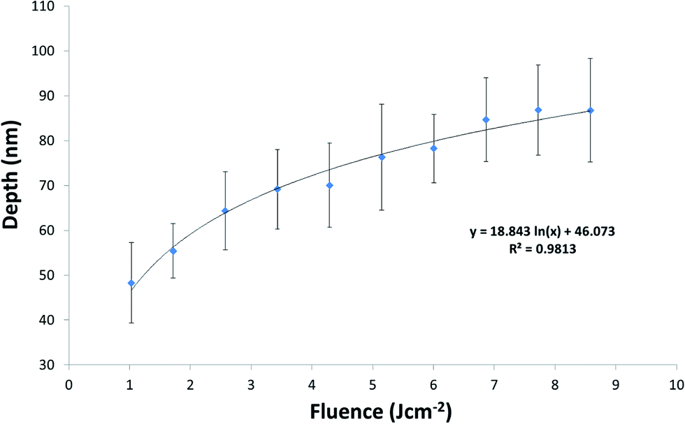 | ||
| Fig. 1 Crater depth measured on AZO layers as a function of laser fluence, based on single-shot experiments. The curved solid line represents the logarithmic function that best fits between data points. RSD (about 20%) was calculated from external reproducibility (3 analyses) and also considering the uncertainty from induced roughness at each crater bottom. | ||
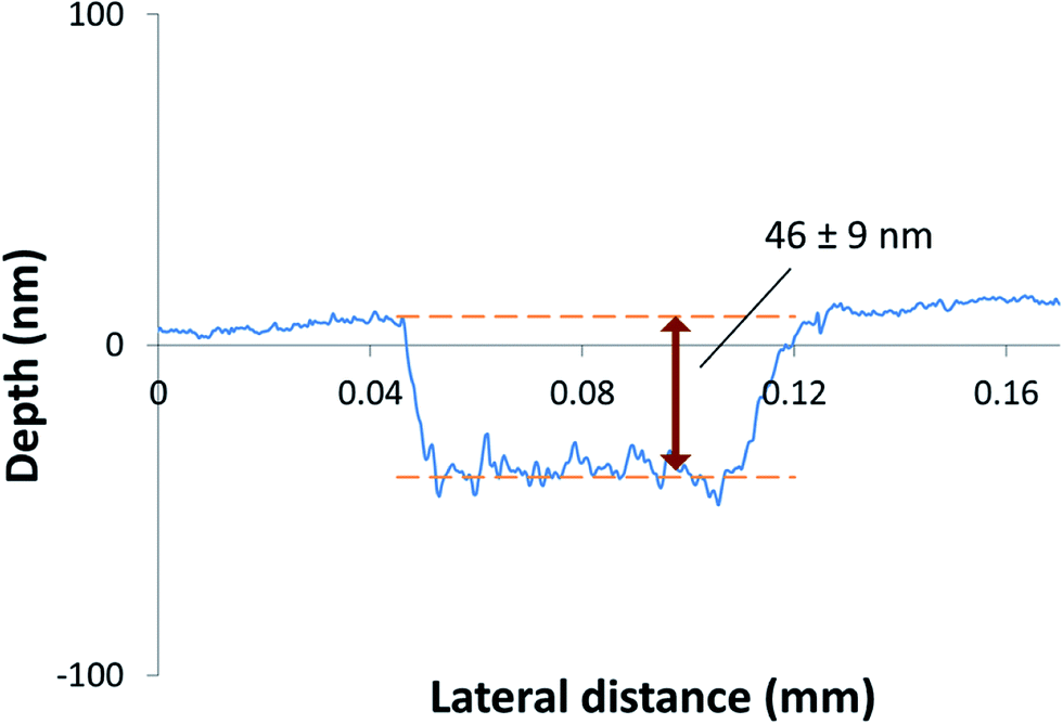 | ||
| Fig. 2 Cross section of the crater obtained on AZO layers after a single laser shot at 1.03 J cm−2. | ||
Further experiments were performed increasing the number of laser shots at a frequency of 1 Hz. In these cases, a linear relationship was obtained between the crater depth and the number of laser shots. For instance, Fig. 3 shows that the AZO coating (500 nm) was completely ablated after 10 laser shots (e.g. average ablation rate of 50 nm per pulse). These results demonstrate the analytical potential of LA-ICP-MS to achieve depth profile analysis with a high depth resolution (10 s of nm). Nevertheless, it should be highlighted that the ablation rate is greatly affected by optical properties of the material and the laser wavelength.
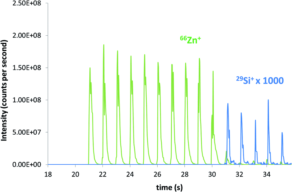 | ||
| Fig. 3 Qualitative depth profile of the Al-doped ZnO layer (thickness 500 nm) deposited on a Si substrate, obtained using 1 Hz and a circular laser spot with a diameter of 65 μm. | ||
Qualitative depth profile analysis of multi-layer CdTe photovoltaic devices
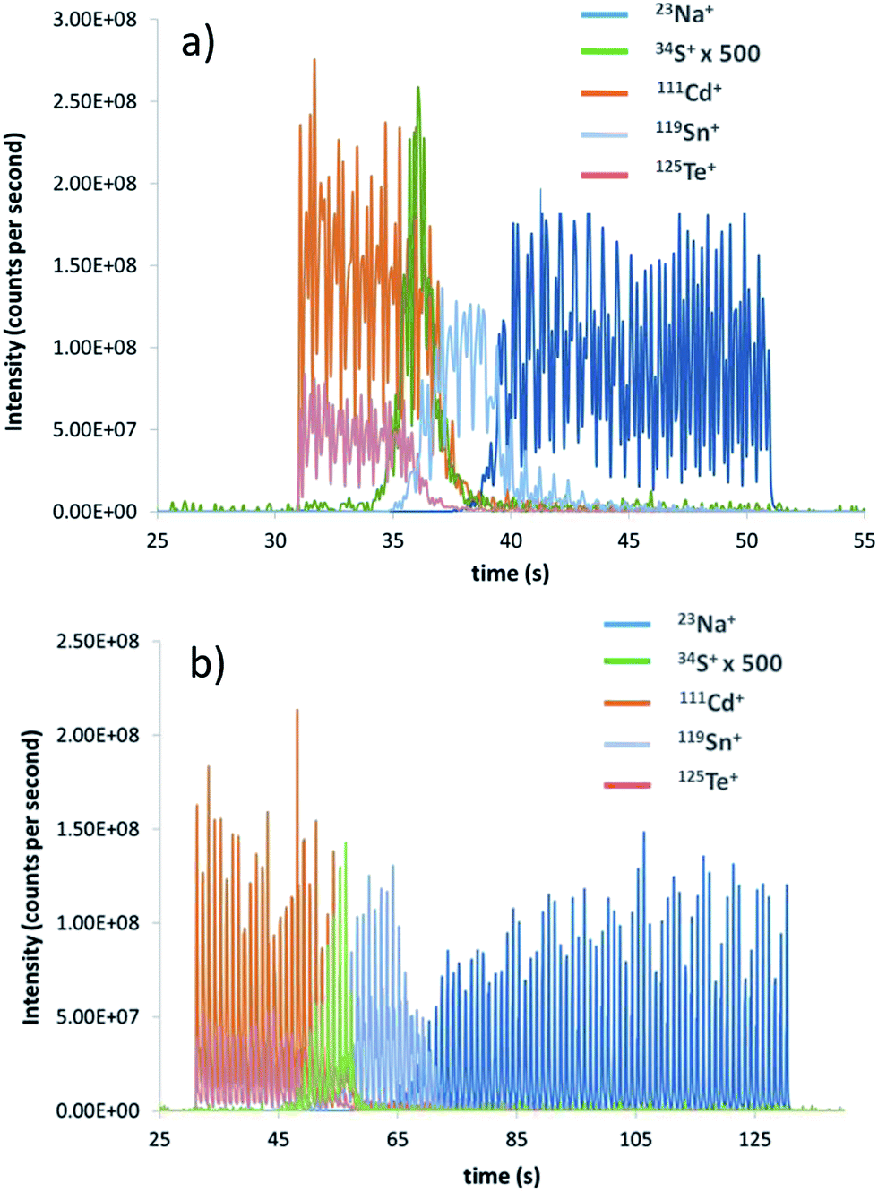
The analytical potential of LA-ICP-MS was investigated for depth profile analysis of multi-layer CdTe photovoltaic devices. In particular, the effect of the spot size and laser frequency on the achieved depth resolution was evaluated and optimized. The laser fluence was fixed at the minimum value (∼1 J cm−2) for each analysis to ensure a minimum penetration depth per laser pulse. During the first 30 seconds, ICP-MS background ion signals were measured, and then the different layers were ablated. The external CdTe layer was analyzed through the measurement of 111Cd+ and 125Te+ ion signals. Afterwards, the CdS layer was resolved with the 34S+ signal and the SnO2 layer was monitored by the 119Sn+ ion signal. Finally, the soda-lime glass substrate was identified through the detection of the 23Na+ ion signal. Fig. 4(a and b) shows the qualitative depth profiles of the multi-layer CdTe photovoltaic cell, obtained at 10 Hz for two different laser spot diameters (65 μm and 160 μm, respectively). In both cases, the different layers can be distinguished but they are not completely resolved. Mixing of coatings is more pronounced using the laser spot diameter of 160 μm due to a higher amount of ablated material per laser shot. Therefore, the spot size diameter of 65 μm was chosen to achieve a better relation between sensitivity and depth resolution.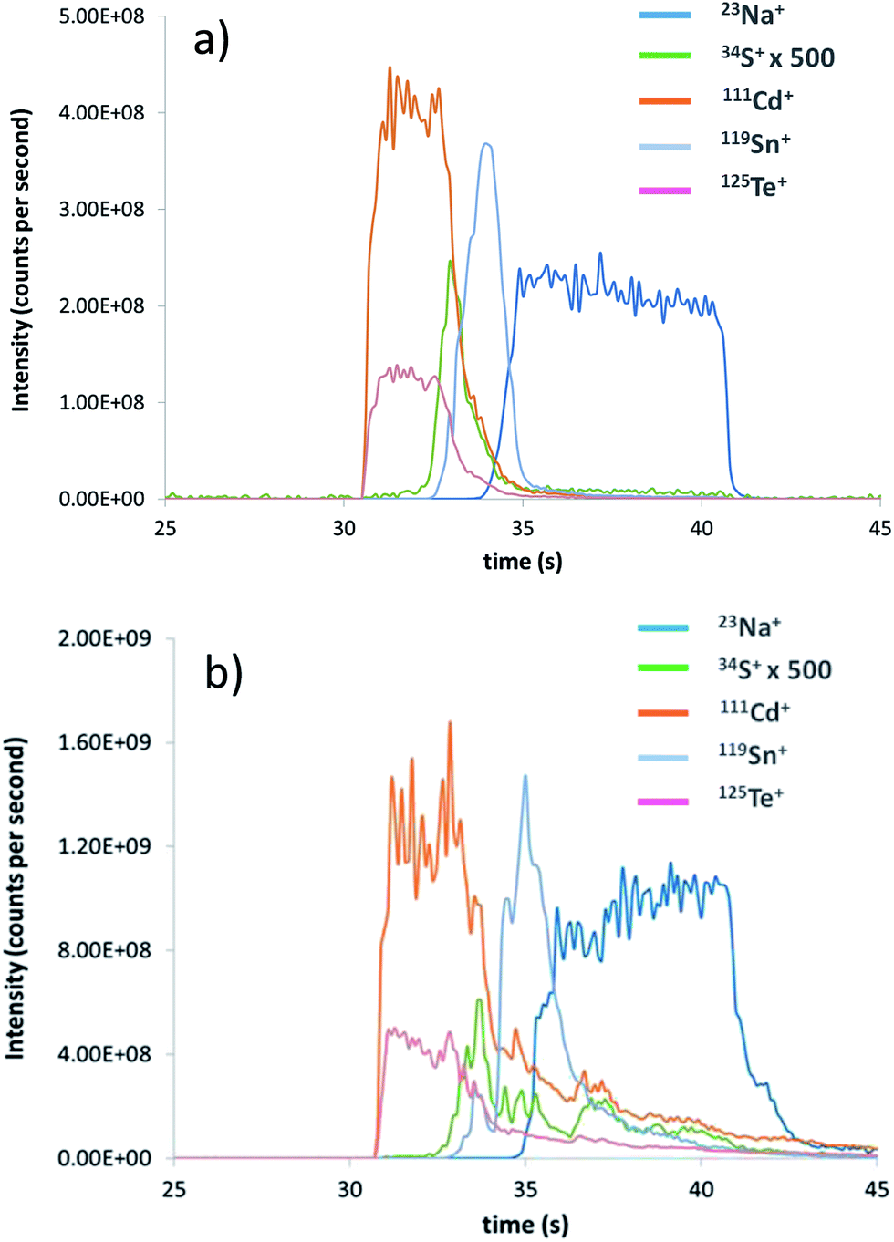 | ||
| Fig. 4 Qualitative depth profiles of multi-layer CdTe photovoltaic cells, obtained using 10 Hz and a circular laser spot with a diameter of: (a) 65 μm; (b) 160 μm. | ||
In order to improve the depth resolution, lower laser repetition rates were also evaluated to further avoid aerosol mixing during aerosol transport. Fig. 5 shows the qualitative depth profiles of multi-layer CdTe photovoltaic cells, obtained at lower laser frequencies, 5 Hz and 1 Hz, using a spot size of 65 μm in diameter. It is observed that at the interfaces between the different layers, ion signals have faster decays using lower laser frequencies. In a ESI figure,† qualitative depth profiles obtained at 5 Hz and at 1 Hz are plotted removing the Sn+ ion signal. This figure clearly shows that working at 1 Hz it is possible to avoid the overlapping between the S+ ion signal and the Na+ ion signal that represents the glass substrate. These results indicate that the use of minimum repetition rates leads to reducing signal mixing, improving depth resolution.
 | ||
| Fig. 5 Qualitative depth profiles of multi-layer CdTe photovoltaic cells, obtained for a circular laser spot diameter of 65 μm at a laser frequency of: (a) 5 Hz; (b) 1 Hz. | ||
At a laser repetition rate of 1 Hz, ion signal oscillations follow the laser frequency due to the fast wash out of the ablation cell. Nevertheless, qualitative depth profiles can be mathematically treated using a smoothing function after ion signal integration of each laser pulse, in order to get a better defined depth profile. Fig. 6 shows the smoothed qualitative depth profile obtained for multi-layer CdTe PV using LA-ICP-MS at 1 Hz. All the layers are clearly resolved, even the thin CdS layer with a thickness of 100 nm.
 | ||
| Fig. 6 Smoothed qualitative profile obtained for multi-layer CdTe PV using a laser frequency of 1 Hz and a circular spot with a diameter of 65 μm. | ||
Fig. 7 shows the qualitative depth profiles obtained for the same multi-layer CdTe PV samples using reference techniques such as GD-TOFMS and SIMS.12 It should be highlighted that qualitative depth profiles obtained by LA-ICP-MS were in good agreement with those obtained by GD-TOFMS and SIMS. These results show that LA-ICP-MS is able to provide fast depth profile analysis with a relatively high depth resolution. Nevertheless, the use of low penetration rates and small laser-induced crater diameters originates the ablation of very small amounts of material that produce a fast transient signal. Sequential mass analysers, such as the quadrupole (Q), might limit the number of monitored analytes per laser pulse due to spectral skew problems.26 Therefore, fast mass analysers such as TOFMS could be recommended to improve multielemental depth profiling capabilities of this technique.
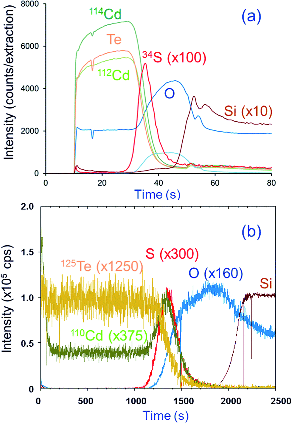 | ||
| Fig. 7 Qualitative depth profiles of multi-layer CdTe photovoltaic cells, obtained using: (a) GD-TOFMS; (b) SIMS. With permission from [C. Gonzalez-Gago, J. Pisonero, N. Bordel, A. Sanz-Medel, N. J. Tibbetts and V. S. Smentkowski, J. Vac. Sci. Technol., 2013, DOI: 10.1116/1.4824164]. | ||
Laser-induced crater shape and morphology
The ablation process at 1 Hz was investigated in more detail during the analysis of multi-layer CdTe PV devices. For this purpose, the shape and morphology of the laser-induced craters were measured at different depths. Fig. 8(a and b) shows the crater profiles measured after different numbers of laser shots, using two spot diameters, 65 μm and 160 μm, respectively. The average penetration depth was found to be a function of the ablated material and the number of laser shots, but it was independent of the spot size. The crater depth was about 1.2 μm (middle of the CdTe layer) after 10 shots, providing an average ablation rate of 120 nm per pulse in this material, which is significantly larger than that obtained for the AZO layers. The laser-induced crater depth was about 2.5 μm (middle of the CdS layer) after 22 shots. At this point, it should be mentioned that the 34S+ ion signal (Fig. 5(b)) was detected during several laser shots, indicating an average ablation rate of the CdS layer (100 nm of thickness) below 50 nm per pulse. Finally, a crater depth of about 3 μm (middle of SnO2 layer) is measured after 33 shots, which results in an average ablation rate of about 50 nm per pulse in this material.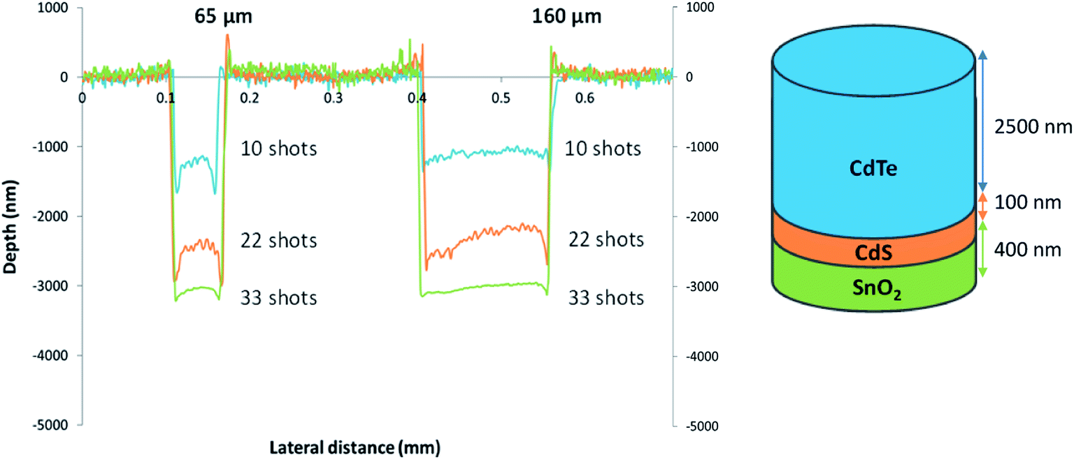 | ||
| Fig. 8 Crater profiles measured in the CdTe PV sample using a profilometer, after different numbers of laser shots (10, 22 and 33) operated at 1 Hz. Crater profiles obtained for two spot sizes with 65 μm and 160 μm of diameter. The number of laser shots was selected to reach each of the different layers of the CdTe PV device. | ||
It was observed that crater profiles were not completely flat (e.g. more ablation was observed at the edge of the crater and some roughness was found at the crater bottom). The convexity of the crater was enhanced at an increasing number of pulses, but it decreased when reaching the SnO2 layer, highlighting the influence of the material composition on the ablation process.
The morphology of the laser-induced craters was investigated using an atomic force microscope (AFM). In particular, the laser-induced roughness was measured at the bottom of the 160 μm spots. Fig. 9 shows the AFM images (a scanning area of 10 μm × 10 μm) after different numbers of laser shots (e.g. different layers of the CdTe PV device). At the surface of the CdTe device (before any ablation process) a grain-structure was observed with an average roughness of about 90 nm (root mean square (RMS) value). Once the CdTe layer was partially ablated, the grain-structure disappeared and some melting processes were detected. In that case, the average roughness measured at the bottom of the laser-induced crater was improved to about 30 nm. This value remained constant after 22 laser shots (CdS layer) but it significantly changed when the SnO2 layer was ablated. At this layer, the average roughness was reduced to about 6 nm, which is also the value measured at the glass substrate (after 100 laser shots). The laser induced roughness and crater shape are factors that have great influence on the depth resolution that can be achieved by LA-ICP-MS but it is observed that they mainly depend on the laser-matter interaction (e.g. composition of the coating).
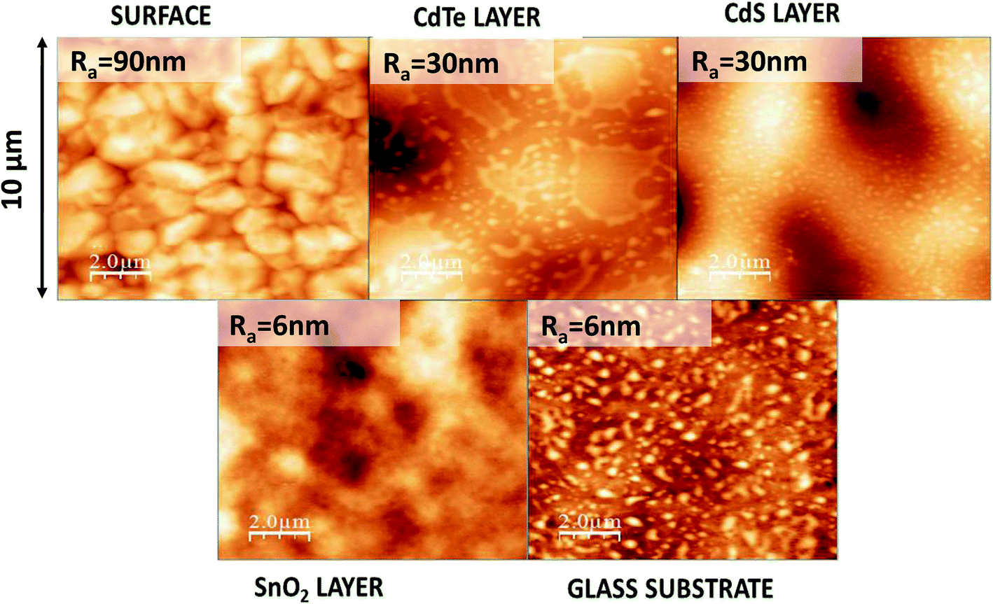 | ||
| Fig. 9 AFM images (top view) with a scan size of 10 μm × 10 μm: (a) the surface of the photovoltaic device; (b) CdTe layer (after 10 shots); (c) CdS layer (after 22 shots); (d) SnO2 layer (after 33 shots); (e) substrate (after 100 shots). Laser was operated at 1 Hz. Laser induced roughness is indicated for each layer. | ||
Conclusions
The analytical capabilities of a flat-top beam ArF* excimer ns-LA-ICP-MS system have been investigated for fast qualitative depth profile analysis of multi-layer CdTe photovoltaic (PV) devices. The influence of the laser fluence on the penetration rate has been initially evaluated using an AZO layer with an original highly-smooth surface. A minimum penetration rate of ∼50 nm per laser pulse has been achieved in a well-defined laser-induced crater. However, the dependence of laser ablation rate on the layer composition significantly affects the depth resolution that can be achieved using LA-ICP-MS for the depth profile analysis of innovative materials.In this study, qualitative depth profiles of the multi-layer CdTe PV device, containing thin layers (∼100 nm), were successfully measured and in agreement with profiles obtained by other reference techniques such as GD-TOFMS and SIMS. Moreover, it has been observed that the depth resolution of the qualitative depth profiles obtained by this LA-ICP-MS system is negatively affected by different parameters, including convex laser-induced crater shapes, large laser spot sizes and high laser repetition rates. Additionally, laser-induced roughness measured at the bottom of the crater has been found to be strongly dependent on the material composition of the ablated layer.
Acknowledgements
Financial support from Photon-Machines and Teledyne CETAC through project FUO-EM-031-13, and from “Plan Nacional de I + D + I” (Spanish Ministry of Science and Innovation and Feder Programme) through MAT2010-20921-C02-02 and FIS2008-06249, are gratefully acknowledged. Dustin Ellis, Laurie LeTarte and Vincent S. Smentkowski from GE-GRC are thanked for useful discussion and other supporting characterization results which are not summarized here. Ana Luisa Martinez from Fundación ITMA is thanked for the support on the ZnO sample preparation.References
- T. Markvart and L. Castañer, Solar Cells: Materials Manufactureand Operation, Elsevier Science & Technology, Oxford, 2005 Search PubMed.
- K. D. Dobson, I. Visoly-Fisher, G. Hodes and D. Cahen, Sol. Energy Mater. Sol. Cells, 2000, 62, 295–325 CrossRef CAS.
- A. Martel, F. Caballero-Briones, A. I. Oliva, R. Castro-Rodríguez, A. Iribarren, P. Bartolo-Pérez and J. L. Peña, Phys. Status Solidi B, 2000, 220, 261–267 CrossRef CAS.
- E. Barojas, R. Silva-González and J. Pantoja-Enríquez, Sol. Energy Mater. Sol. Cells, 2006, 90, 2235–2240 CrossRef PubMed.
- J. Pantoja-Enríquez, E. Gómez-Barojas, R. Silva-González and U. Pal, Sol. Energy Mater. Sol. Cells, 2007, 91, 1392–1397 CrossRef PubMed.
- K. D. Rogers, J. D. Painter, M. J. Healy, D. W. Lane and M. E. Ozsan, Thin Solid Films, 1999, 339, 299–304 CrossRef CAS.
- X. Wu, S. Asher, D. H. Levi, D. E. King, Y. Yan, T. A. Gessert and P. Sheldon, J. Appl. Phys., 2001, 89, 4564–4569 CrossRef CAS PubMed.
- P. Boieriu, R. Sporken, A. Adriaens, Y. Xin, N. D. Browning and S. Sivananthan, Nucl. Instrum. Methods Phys. Res., Sect. B, 2000, 161–163, 975–979 CrossRef CAS.
- M. Emziane, K. Durose, D. P. Halliday, N. Romeo and A. Bosio, Thin Solid Films, 2006, 511–512, 66–70 CrossRef CAS PubMed.
- O. Koudriavtseva, A. Morales-Acevedo, Y. Kudriavtsev, S. Gallardo, R. Asomoza, R. Mendoza-Perez, J. Sastre-Hernandez and G. Contreras-Puente, Appl. Surf. Sci., 2008, 255, 1423–1426 CrossRef CAS PubMed.
- R. Escobar-Galindo, R. Gago, A. Lousa and J. M. Abella, Trends Anal. Chem., 2009, 28, 494–505 CrossRef CAS PubMed.
- J. Pisonero, N. Bordel, C. Gonzalez de Vega, B. Fernández, R. Pereiro and A. Sanz-Medel, Anal. Bioanal. Chem., 2013, 405, 5655–5662 CrossRef CAS PubMed.
- C. Gonzalez-Gago, J. Pisonero, N. Bordel, A. Sanz-Medel, N. J. Tibbetts and V. S. Smentkowski, J. Vac. Sci. Technol., A, 2013, 31, 06F106 Search PubMed.
- L. Lobo, B. Fernandez, R. Pereiro, N. Bordel, E. Demenev, D. Giubertoni, M. Bersani, P. Honicke, B. Beckhoffd and A. Sanz-Medel, J. Anal. At. Spectrom., 2011, 26, 542–549 RSC.
- J. Pisonero, A. Licciardello, A. Hierro-Rodríguez, C. Quirós, A. Sanz-Medel and N. Bordel, J. Anal. At. Spectrom., 2011, 26, 1604–1609 RSC.
- J. Pisonero, B. Fernandez and D. Günther, J. Anal. At. Spectrom., 2009, 24, 1145–1160 RSC.
- J. Pisonero and D. Gunther, Mass Spectrom. Rev., 2008, 27, 609–623 CrossRef CAS PubMed.
- D. Bleiner, A. Plotnikov, C. Vogt, K. Wetzig and D. Günther, Fresenius. J. Anal. Chem., 2000, 368, 221–226 CrossRef CAS.
- L. Balcaen, J. Lenaerts, L. Moens and F. Vanhaecke, J. Anal. At. Spectrom., 2005, 20, 417–423 RSC.
- J. Pisonero, J. Koch, M. Walle, W. Hartung, N. D. Spencer and D. Günther, Anal. Chem., 2007, 79, 2325–2333 CrossRef CAS PubMed.
- D. Günther, R. Frischknecht, C. A. Heinrich and H. J. Kahlert, J. Anal. At. Spectrom., 1997, 12, 939–944 RSC.
- M. Guillong, I. Horn and D. Günther, J. Anal. At. Spectrom., 2002, 17, 8–14 RSC.
- J. Mikova, J. Kosler, H. P. Longerich, M. Wiedenbeck and J. M. Hanchar, J. Anal. At. Spectrom., 2009, 24, 1244–1252 RSC.
- M. G. Babechuk, B. S. Kamber, A. Greig, D. Canil and J. Kodolanyi, Geochim. Cosmochim. Acta, 2010, 74, 1448–1470 CrossRef CAS PubMed.
- D. Bleiner, Z. Chen, D. Autrique and A. Bogaerts, J. Anal. At. Spectrom., 2006, 21, 910–921 RSC.
- W. Müller, M. Shelley, P. Miller and S. Broude, J. Anal. At. Spectrom., 2009, 24, 209–214 RSC.
- D. Bauerle, Laser Processing and Chemistry, Springer-Verlag, 2011 Search PubMed.
- M. Stafe, C. Negutu, N. N. Puscas and I. M. Popescu, Rom. Rep. Phys., 2008, 62, 758–770 Search PubMed.
Footnote |
| † Electronic supplementary information (ESI) available: Figure: qualitative depth profiles of multi-layer CdTe photovoltaic cells, obtained for a circular laser spot diameter of 65 μm at a laser frequency of: (a) 5 Hz and (b) 1 Hz. In particular, the Sn+ ion signal that represents the SnO2 layer has been removed to show in more detail overlapping between S+ and Na+ ion signals. See DOI: 10.1039/c4ja00196f |
| This journal is © The Royal Society of Chemistry 2015 |