 Open Access Article
 This Open Access Article is licensed under a
 Creative Commons Attribution 3.0 Unported Licence
Localized dealloying corrosion mediated by self-assembled monolayers used as an inhibitor system
B. R.
Shrestha
a,
A.
Bashir
a,
G. N.
Ankah
a,
M.
Valtiner
a and
F. U.
Renner
*ab
aMax-Planck-Institut für Eisenforschung GmbH, Max-Planck-Straße 1, D-40237 Düsseldorf, Germany. E-mail: frank.renner@uhasselt.be
bInstitute of Materials Research (IMO), Hasselt University, Wetenschapspark 1, B-3590 Diepenbeek, Belgium
First published on 29th April 2015
Abstract
The structure and chemistry of thiol or selenol self-assembled organic monolayers have been frequently addressed due to the unique opportunities in functionalization of materials. Such organic films can also act as effective inhibition layers to mitigate oxidation or corrosion. Cu–Au alloy substrates covered by self-assembled monolayers show a different dealloying mechanism compared to bare surfaces. The organic surface layer inhibits dealloying of noble metal alloys by a suppression of surface diffusion at lower potentials but at higher applied potentials dealloying proceeds in localized regions due to passivity breakdown. We present an in situ atomic force microscopy study of a patterned thiol layer applied on Cu–Au alloy surfaces and further explore approaches to change the local composition of the surface layers by exchange of molecules. The pattern for the in situ experiment has been applied by micro-contact printing. This allows the study of corrosion protection with its dependence on different molecule densities at different sites. Low-density thiol areas surrounding the high-density patterns are completely protected and initiation of dealloying proceeds only along the areas with the lowest inhibitor concentration. Dealloying patterns are highly influenced and controlled by molecular thiol to selenol exchange and are also affected by introducing structural defects such as scratches or polishing defects.
Introduction
Corrosion is a major problem in various technical fields from the oil, gas, and chemical industry1 to biomedical implants2,3 or infrastructures.4 In particular, premature catastrophic failure of structural components can be initiated by corrosion and poses a considerable risk for the environment and human society. Several studies report on the huge economical loss caused by corrosion each year. Considerable effort has therefore been made to design and develop complex alloys which deliver good mechanical properties as well as excellent corrosion resistance. Unfortunately, such corrosion resistant alloys often contain large quantities of expensive elements such as Cr, Ni, or Mo. One further way to mitigate corrosion of materials in applications is the use of inhibitors, and organic systems are today widespread. Especially the oil and gas industry is a large consumer of organic inhibitors.1 At the same time there is also a large research effort to find environmentally friendly inhibitors.5 The effect of inhibitors varies often depending on (even slight) changes in the environment, temperature, or protected materials, even “from one oil well to another”.1 A better understanding of the underlying mechanisms of corrosion protection by organic inhibitors is therefore needed. A true mechanistic understanding on the atomic and molecular level is so far widely lacking. Thiol and selenol based films have been employed for oxidation and corrosion protection of copper.6–10 The formation of self-assembled organic monolayer films (SAMs) based on various thiols and selenols has been widely studied due to the unique opportunities in functionalization of materials. In particular, with the wide and detailed knowledge of the structure and chemistry of such often highly ordered films on the molecular level, SAMs provide a promising model system for fundamental corrosion studies.Molecular self-assembly is controlled through a strong covalent bonding to a substrate and non-covalent interactions between the molecules such as van der Waals forces, or π–π interactions.11,12 Common examples include the formation of liquid crystal phases, micelles, vesicles, and Langmuir films.13 Many SAMs are based on thiol or lately selenol molecules on Au, Ag, Pd, or Cu substrates.11–14 The large possible variety (Fig. 1a) to combine the S- or Se-head group15–17 with different organic ends or chains enables many possibilities to control the structure of SAMs films.18 Recent research has concentrated on increasing the stability of the films by offering structural changes via the exchange of molecules. For Au substrates, selenols were found to be more stable than thiol-based molecules.18 In general the stability of SAMs depends on the substrate symmetry and atomic distances in the surface plane as well as on the interplay with the chain interactions. The ability to form a well-ordered surface film thus depends often on the chosen chain length, an odd or even number of carbon atoms18 in the chain, or the existence of aromatic building blocks.6,19 The presence of such SAMs plays an important role in dealloying.
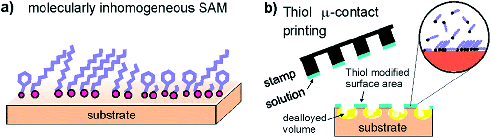 | ||
| Fig. 1 (a) Schematic showing the formation of an organic SAMs layer on a metal substrate. (b) Schematic showing the formation of SAMs patches during stamping and dealloying. | ||
Dealloying is one form of corrosion where less noble element/s (one or more) are selectively dissolved. The nobler element(s) accumulates or diffuses on the surface eventually leading to passivation. At lower overpotentials above the equilibrium potential of Cu, bare Cu3Au (111) surfaces are covered by an ultrathin film of Au of about 3 monolayers (ML), which protects from further selective dissolution of Cu, as was described earlier.20,21 At intermediate overpotentials, 10–15 ML thick Au islands are formed, before the protective effect of the Au barrier layer breaks down at the so-called critical potential (Ec) and bulk nanoporous Au is formed22,23 due to uniform dealloying. But the uniform dealloying can be overruled by the application of SAMs.23–26 We have recently started research on the effects of SAMs on alloys23–25 based on noble metal binary systems.27 Cu–Au alloy substrates covered by SAMs show a different dealloying mechanism compared to bare surfaces. The organic surface layer inhibits dealloying corrosion of noble metal alloys by a suppression of surface diffusion. After passivity breakdown at higher applied potentials, dealloying proceeds in localized regions. With progressing dealloying, the process results in the appearance of surface cracks which form due to an accumulation of local stress related to a volume shrinking of nanoporous gold during dealloying.28 Together with the high level of control over the structural quality of self-assembled organic films, the system is a promising inhibitor model for understanding localized dealloying corrosion on the molecular scale.
Moreover, laterally structured SAMs can be applied on surfaces employing micro-contact printing (μCP) using simple polydimethylsiloxane (PDMS) stamps.29–33 The process is sketched in Fig. 1b. This approach includes local chemical reactions31–33 and possibly also a local exchange of molecules in the monolayer.
Here, we report initial results of a larger research effort where we want to employ the great opportunities offered by molecularly homogeneous and heterogeneous self-assembled organic films used as model inhibitor films towards dealloying and in particular localized corrosion. The use of patterned SAMs and their effect on dealloying is well suited for in situ atomic force microscopy to reveal molecular and atomic scale mechanisms of corrosion and corrosion protection. We will further discuss first results of a controlled exchange of thiol and selenol molecules to further manipulate the internal structure of the self-assembled inhibitor monolayers and the respective effect on dealloying corrosion.
Experimental
Standard H2SO4 was bought from Sigma Aldrich and diluted to get the required 0.1 M solution. Thiophenol (BT), benzeneselenol (BSe) were purchased from Aldrich and used without further purification. Self-assembled monolayers (SAMs) of target molecules were prepared by immersing the Au(111) substrates into a 1 mM (BT) and 4mM (BSe) ethanolic solution at room temperature. After the allotted immersion time, the samples were removed from the respective solutions, thoroughly rinsed with copious amounts of the solvent (ethanol) and finally dried in a stream of nitrogen. All solutions were freshly prepared before each experiment.We report the results of the characterization by different techniques including in situ electrochemical dealloying by Atomic Force Microscopy (AFM), the exchange of organic molecules (BSe, BT) by Quartz Crystal Microbalance Dissipation (QCMD) and ex-situ Scanning Electron Microscopy after electrochemical dealloying.
(i) In situ electrochemical dealloying by atomic force microscopy
Cu3Au (111) single-crystals with an orientation misfit less than 0.1° and polycrystalline alloys were obtained from MaTecK GmbH (Germany). The surfaces were prepared by repeating cycles of sputtering and annealing in an UHV chamber. The self-assembled monolayers (SAMs) were printed on well-prepared Cu3Au crystals by using a polydimethylsiloxane (PDMS) stamp with 3 μm × 3 μm square patterns. Cu3Au crystals were patterned by micro-contact printing (μCP), to yield a surface consisting of target molecules. The desired SAMs were fabricated from the stamp after exposing them to the 1 mM solutions of target molecules. In situ AFM experiments on Cu3Au surfaces were carried out under potentiostatic conditions in 0.1 M H2SO4. A platinum wire was used as a counter electrode and a silver/silver-chloride (Ag/AgCl) micro-reference electrode was used as reference electrode. The reference electrode was homemade according to the protocol published by Hassel et al.34 All potentials in this paper are referred to Ag/AgCl. Prior to the AFM experiments, the tip was cleaned in conc. sulfuric acid for 2 minutes, thoroughly rinsed with deionized water and ethanol and dried in a stream of nitrogen. In situ-AFM experiments were performed using a JPK NanoWizard I AFM (JPK Instruments AG, Berlin, Germany). A syringe pump (Micromechatronics AG, Germany) was used for pumping the electrolyte. For electrochemical control, a VoltaLab 40 potentiostat/galvanostat (Radiometer Analytical, France) was used. IR-drop compensation was performed using the current-interrupt method compensating for 95% of the measured IR-drop.(ii) Adsorption and or replacement of organic molecule experiment by QCMD
Gold quartz crystals used in the QCMD experiments were purchased from Q-sense. 4 mM solutions of BT and BSe were used for this experiment. Firstly, ethanol was passed into the QCMD system (Q-Sense E1 from Biolin Scientific, Finland) to minimize the drift of the system. The data obtained in ethanol are used as the base line of zero, as all the SAMs solutions were prepared in ethanol. The drift in the experiments is less than 0.5 Hz h−1. Once the drift is satisfactory, the adsorption of BT, BSe and the exchange of BT with BSe, or vice versa, on polycrystalline gold quartz crystals were measured during the flow of the respective solution.(iii) Scanning electron microscopy after electrochemical dealloying
Polycrystalline Cu3Au alloys were obtained from MaTecK GmbH (Germany) in polished form. The samples were first dipped in 0.1 M H2SO4 for 1 hour for chemical cleaning. Then BT SAMs was deposited onto the surface by exposing the sample in 4 mM SAMs solution, and an eventual exchange of the BT SAMs was done by BSe by exposing the surface onto the respective solution. One cycle of CV was performed from −0.2 V to 1.0 V vs. Ag/AgCl in 0.1 M H2SO4 at 10 mV s−1 and finally SEM images were taken using a Zeiss Leo scanning electron microscope.Results and discussion
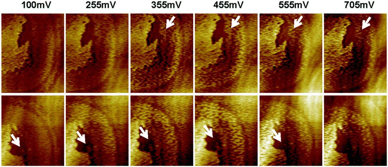
Localized and inhomogeneous corrosion, the likely case in any realistic application, is much less understood than the homogeneous case. The application of structured thiol SAMs by a pre-formed PDMS stamp is a well established simple lithography method. We have fabricated hexadecanethiol (HDT) SAMs patterns of 3 μm × 3 μm, separated by a gap of 2 μm, as an inhomogeneous film of a model inhibitor. Fig. 2 shows the sequence of AFM images obtained by following the potential-dependent initiation of the dealloying process on the surfaces protected by the patterned thiol inhibitor film by in situ atomic force microscopy. Fig. 2a represents the used stamp with a typical regular SAMs pattern on pure gold. For our experiment we have intentionally pressed the stamp slightly harder on the Cu3Au (111) surface in order to obtain a halo or additional ring of a less dense thiol phase around the central patch (Fig. 2b). For the experiments, we have chosen to image an area including 4 patches of HDT SAMs. Two of these show a macroscopic defect, which stems from a presumed defect in the used stamp. The defects allow us to better correlate the structural changes and changes in the surface morphology around the patterns. | ||
| Fig. 2 Alloy corrosion studied with patterned inhibitor films by in situ AFM. We show the initial surface roughening and the evolution of the structure up to +805 mV. (a) Typical pattern on pure Au without halo effect (ideal press). The used pattern has been pressed harder to obtain a low-density halo around the central patch at (b) 100 mV, (c) 255 mV, (d) 355 mV, (e) 455 mV, (f) 555 mV, (g) 705 mV, and (h) 805 mV. | ||
The sequence of in situ images (Fig. 2b–h) from initially 100 mV to 805 mV does not show the typical Au islands, which form on bare Cu3Au (111).20,21 The mentioned (flat) islands indicate a regime of slightly higher initial Cu dissolution below the critical potential. At 805 mV, which is close to the critical potential of bare Cu3Au surfaces, dealloying clearly occurs in the central part between the applied thiol patches (area indicated by a white circle). Yet, the part of the surface where no thiol film or islands (in the AFM images) can be seen is also still completely stable as revealed by the flat morphology showing the typical crystalline steps of intact well-prepared single-crystalline surfaces.
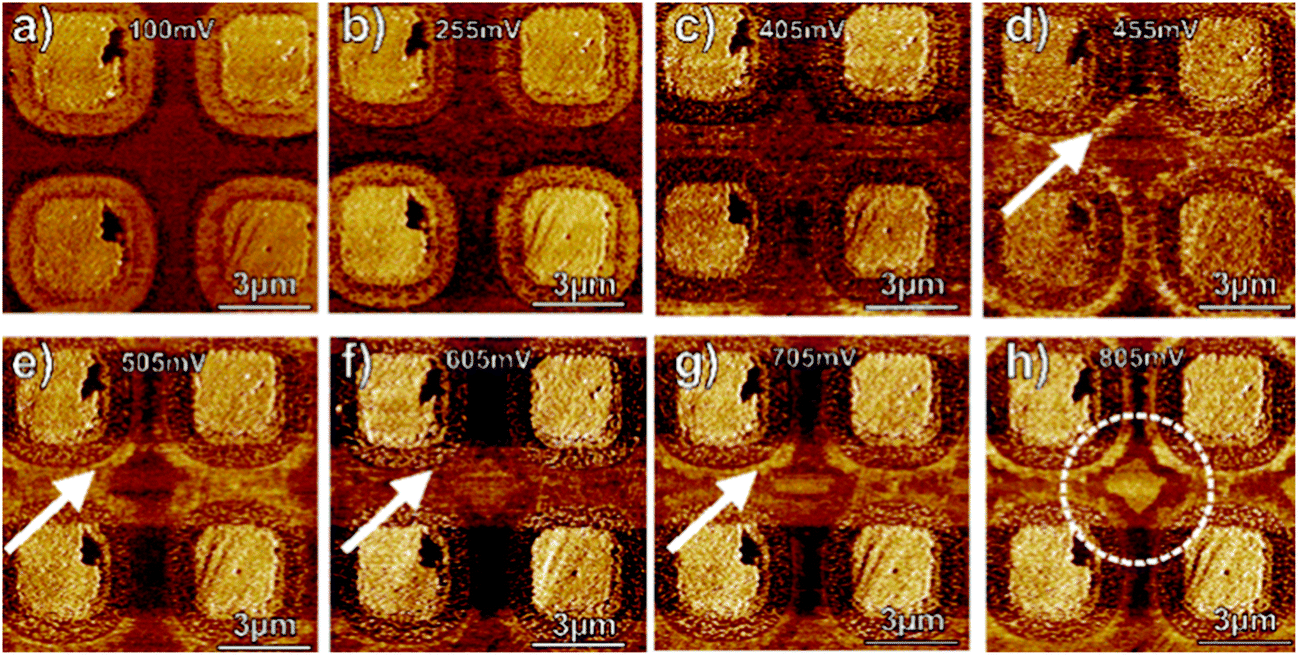
Fig. 3 shows a selection of enlarged sections focusing on the thiol SAMs around the two macroscopic defects of the sequence shown in Fig. 2. The central part, representing a dense thiol SAMs, does not show considerable changes of the local film morphology although it appears slightly rougher at higher applied potentials. In contrast, the halo shows major changes. At 100 mV the halo is formed by a smooth continuous film with a clear height contrast in comparison to the central dense SAMs. This directly points to a possible lying-down thiol phase within the halo film. The white arrows in the upper row of Fig. 3 follow a thiol island, which appears to be stable over the experimental run. The surrounding of this discernible island has nevertheless considerably changed at 705 mV. The initial dense and continuous lying-down phase has developed into islands covering the area of the initial halo. An interesting detail is that this area of the initial halo appears at the end with a clear height difference of the underlying substrate towards the outer surface which appears slightly lower. The same processes are mirrored in the lower row where the lower white arrow points to a thiol island which initially grows but finally vanishes completely. Such phenomena of evolution and disappearance of islands generated from organothiolate35 SAMs/Au (111) have previously been observed. Fig. 4 focuses on the image obtained at 805 mV and reveals a height difference of the surface below the thiol islands of the halo and the outer (Au-enriched) surface of exactly 2 monoatomic steps (about 0.48 nm, a double step on Au (111)). On the outer surface mono-atomic steps are present (about 0.24 nm step height). The higher resolution image also reveals that the formed thiol islands within the halo area have the same height as the initial SAMs of the inner dense core of the applied pattern. Above the critical potential, at 805 mV, the area in between the thiol SAMs undergoes dealloying, leaving part of the surface in the vicinity of the halo region unaltered. Thus, an area in the form of a second ring becomes evident around the printed central dense SAMs where apparently thiol molecules again influence the stability of the surface and protect from a dealloying attack.
 | ||
| Fig. 3 Magnified view of the structure after stepping the potential to 100 mV, 255 mV, 355 mV, 455 mV, 505 mV, 605 mV, 705 mV and 805 mV. The same potential (stated on the top) was applied to the sample shown on the top and below. | ||
 | ||
| Fig. 4 High resolution atomic force micrograph showing the structure of the Cu3Au alloy surface after stepping and holding the potential at 805 mV. | ||
Fig. 5 depicts the AFM images of Fig. 2 in phase mode. The phase signals along the images indicate a reason for the observed second or outer halo area. At lower potentials, only one homogeneous halo ring around the central part is visible (Fig. 5a–c). But at higher potentials, another bright halo ring becomes visible (Fig. 5d–h) due to diffusion of thiol from the initial halo. Thus, we interpret this region as a lower-density thiol phase. This emerging second ring (see white arrow) extends right to the middle area of the image where dealloying commences (white circle in Fig. 5h).
 | ||
| Fig. 5 Phase images of the structure after stepping the potential to 100 mV, 255 mV, 355 mV, 455 mV, 505 mV, 605 mV, 705 mV and 805 mV. | ||
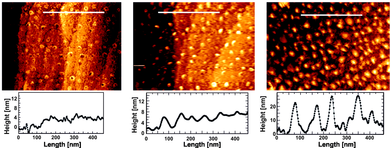
Fig. 6 and 7 focus on the area where dealloying is clearly visible at potentials of 805 mV or higher. The first contrasting and important feature to our previous study on bare Cu3Au surfaces20,21 is the fact that no flat Au islands form below the onset of bulk dealloying at the critical potential. Without thiols 10–15 ML thick Au islands are formed on Cu–Au alloys at intermediate potentials well below the critical potential. Above the critical potential finally a bulk nanoporous Au network is formed due to passivity breakdown of the Au film. The suppression of the formation of Au islands was nevertheless observed in experiments where a continuous self-assembled thiol film was applied23 and localized nanoporous etch pits appeared at the anodically shifted critical potential. The site of dealloying is given in this experiment by the applied pattern of SAMs and line profiles in the attacked regions clearly show the progression of dissolution (Fig. 6c and f). Initially at 805 mV, the observed bottom surface is about 1 nm lower than that of the surrounding area, and later at 905 mV, the pitted area is about 3 nm deep (Fig. 6c and f). To accumulate about 1 ML of Au, Cu from about 4 ML of Cu3Au has to be removed by selective dissolution. In other words, a pit of 3 nm points to an accumulated Au thickness of about 1 nm, i.e. the dealloying process is still in an initial state. Full ligaments of a nanoporous Au structure are typically in the order of 10–40 nm.
 | ||
| Fig. 6 High resolution AFM images and height profiles along the indicated lines at 805 mV (a–c) and 905 mV (d–f). | ||
 | ||
| Fig. 7 High resolution atomic force micrographs showing the structure of the inner region with visible dealloying while holding the potential at 805 mV at different times. | ||
The evolution of the morphology at the locally attacked sites during dealloying is also interesting to follow. Initial individual islands are first forming in low density before dealloying proceeds into the bulk. Fig. 7 shows one sequence recorded from the inner part of an area undergoing dealloying. The receding bottom surface is initially following the original atomic steps of the well-prepared surface. With further dealloying, the interface develops a higher roughness and the islands cover the interface more densely. Here, the island formation is at potentials close to Ec, the first step in the evolution of nanoporosity. The surface morphology clearly resembles the island formation on bare Cu3Au surfaces at much lower potentials and can be clearly distinguished from other alloys such as Cu–Pd.36
The in situ AFM imaging was stopped at 905 mV and SEM images, such as shown in Fig. 8a, were taken. Dealloying processes have visibly taken place over a large sample area and it always occurs at the farthest site from the printed SAMs patches. The dense central thiol SAMs as well as the first halo around this central area is visible. Comparing the SEM images with the in situ AFM images, it can be inferred that a large part of the area between the SAMs patches and also their halo is clearly free of dealloying and the actual dealloying has taken place only in a limited area. Few of these potential dealloying sites are fully protected allowing no visible dealloying at all. Part of the thiol-free area was therefore apparently protected from massive Cu dissolution. We nevertheless note here that some limited number of spots have undergone a more severe dealloying attack. These originate at sites where visibly one of the central thiol patches is missing, i.e. the printing process has not properly succeeded and dealloying has locally spread out over a larger region. Due to such flaws and their associated inhomogeneous current distribution, it is not possible to correlate the measured total current with the observed changes in morphology, in particular, the local observation by AFM. Yet, since dissolution is a kinetically fast process, we can conclude that the applied potentials are homogeneous over the surface.
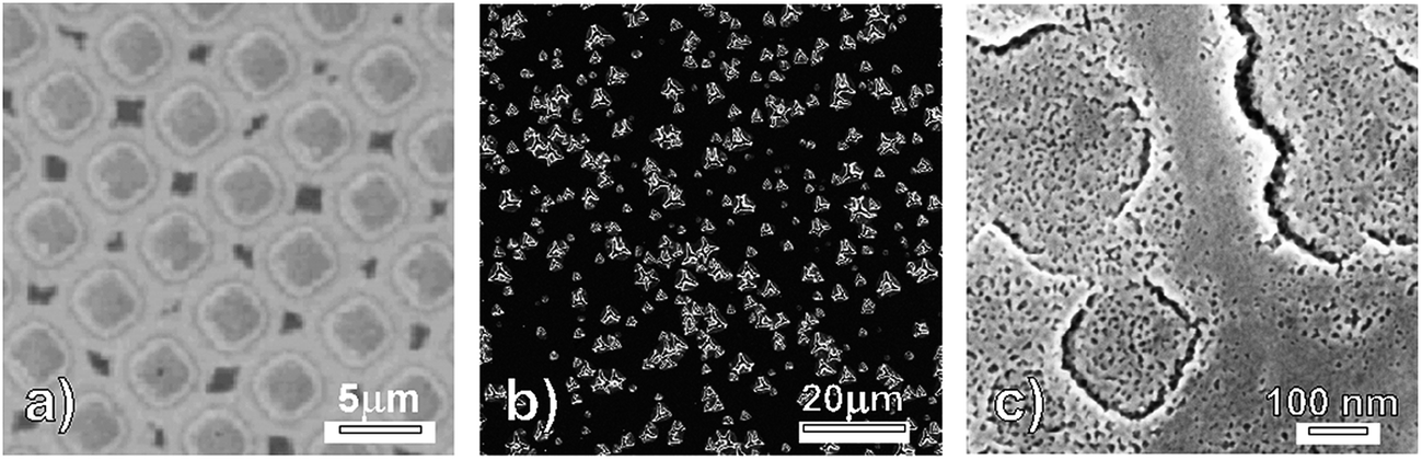 | ||
| Fig. 8 (a) SEM image of the Cu3Au (111) surface after the in situ AFM experiment up to 905 mV. (b) Image after dealloying of a Cu3Au polycrystalline surface modified with a continuous self-assembled mixed aminobenzenethiol monolayer. (c) SEM image of a grain surface partly free of thiols after a potential step to 1.3 V for 15 s and a CV. | ||
When we compare dealloying from patterned thiol-modified alloys (current study) with dealloying from homogeneously thiol-modified alloys (previous study23) a few interesting aspects can be shown. With the printed pattern of SAMs, we could control the site where dealloying corrosion initiates. In contrast, on homogeneously covered thiol-surfaces a stochastic distribution of dealloying sites has been described.23 For these sites, the separation is much larger as natural structural inhomogeneity than for example the typical domain size as exemplified for a surface initially modified by a mixed aminobenzenethiol film, 24 shown in Fig. 8b. Still an open question therefore is the nature of the potential initiation site. Approaching this problem using pre-patterned inhomogeneous SAMs may well contribute to the molecular-level understanding of the inhibition effect. A further approach is represented in Fig. 8c where an initially continuous ethanethiol monolayer formed on Cu3Au was partially removed by a short oxidative potential step. The effective removal of ethanethiol by such an oxidation step has been observed on Au by in situ electrochemical surface-sensitive X-ray diffraction, employing synchrotron light.25 This process results in an inhomogeneous dealloying process (Fig. 8c). The driving force for these experiments has been to advance our understanding of the effect of structural inhomogeneity on the onset of dealloying for inhibitor-covered surfaces. Yet chemical or molecular inhomogeneity will potentially play a large role and provides further means to manipulate and control the stability of inhibitor-covered alloy surfaces.
Molecular inhomogeneity can be deliberately introduced by exchanging part of the applied SAMs on the molecular level and can be simultaneously monitored by QCMD as the sensitivity of the technique is few ng cm−2. Fig. 10 shows the areal mass change on gold quartz crystals during the adsorption and exchange of BT with BSe or vice versa. The base line shown until 300 seconds is the data obtained while ethanol was passed into the QCMD. Since all SAMs were assembled in ethanol, ethanol was referenced as the base line. As shown in Fig. 9, after 300 seconds of passing ethanol, solutions containing SAMs were passed and their adsorption increases the areal mass in each case. In two other experiments, a different (BT or BSe) molecule was passed after 600 seconds, which either increased (see red line) or did not show any effect (see blue line) on the areal mass. Some limited disturbance of the measurement system is caused during the process of solution change.
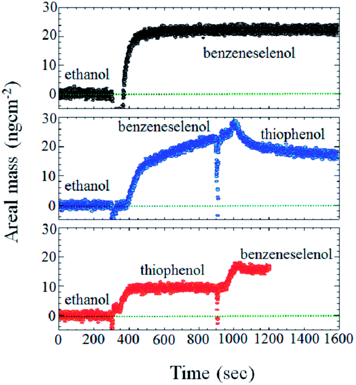 | ||
| Fig. 9 Plot showing the areal mass change on Au with time during the adsorption or adsorption and exchange of respective molecules. The red line first shows the adsorption of the BT molecule and then the replacement by BSe. The black line represents the curve obtained during the adsorption of BSe and the blue line shows the adsorption of BSe and its potential exchange with BT. | ||
Kaefer et al.37 report molecular areas of 28.8 Å2 and 38.5 Å2 for BSe and BT, resulting in about 85 ng cm−2 and 43 ng cm−2 for a monolayer, respectively. We see in Fig. 9 that our measured values on a rough sample are lower but show the same ratio of about 2. Thus, a SAMs of BSe or BT is formed when the respective molecules are passed to the crystal (see black and red line) but when replacing the BT SAMs by BSe, we find that it is to about 80% exchanged. When BT was passed the areal mass decreased slightly, indicating some replacement of BT molecules as well. Interestingly, the exchange from a full BSe SAMs exhibits slower exchange kinetics, compared to exchanging BT by benezeneselenol. Yet, both ways converge to coverage of approximately 80% BSe and 20% BT.
Based on the exchange, we expect different thin-film properties, and as such a moderation of the dealloying process. These results on molecular exchange have been then applied to a polycrystalline Cu3Au foil for a first test of respective changes in the behavior during dealloying corrosion. Fig. 10 shows the SEM recorded after the exchange of BT SAMs by BSe according to Fig. 9 (red curve). As seen in Fig. 9, the mass obtained during exchange of BT with BSe is not the same as when BSe alone is passed. So, we conclude that the exchange process did not replace BT by 100%. The polished surface was then dealloyed by a potential sweep from −200 mV to 1000 mV and back with a rate of 10 mV s−1. As a result, the alloy is non-homogeneously dealloyed as can be seen in Fig. 10 where the brighter regions represent the dealloyed regions. Round as well as slightly elongated dealloyed areas with typical dimensions of between 1 μm and maximum 20 μm can be distinguished. Some polishing lines are also visible but, in general, the dealloyed regions are rather independent of these defect lines. The larger dealloyed regions, however, often show cracks along the crossing polishing lines. Independent of the cracking behavior we can conclude that the exchange process did indeed significantly change the dealloying initiation, as shown in Fig. 8b and 10b. With a homogeneous SAMs, dealloying occurs purely local, producing round areas in the beginning which later form cracks (Fig. 8b) but we see dealloying in more elongated and outspread forms indicating dealloying is not purely local anymore (Fig. 10b). Routes to control the growth and behavior of organic molecules on metal surfaces are also important for functionalized interfaces, for example in sensor applications. Inhibition of corrosion is another economically important process where metal–organic interfaces play a crucial role. Most of today's inhibitors are organic in nature.1 Dealloying of Cu–Au alloys is due to clearly distinguished stages of surface evolution (ultrathin film – Au islands – nanoporosity) of the bare substrate and the localized nature of SAMs-modified (inhibited) surfaces, an in our view interesting model system. Here, we addressed different aspects of control over a localized corrosion process on Cu–Au alloys. Printed structured patterns produce a local variation of different inhibitor densities and enabled us, by varying the basic dimensions of the pattern, to address the important questions of inhibitors and the mechanistic understanding of material (surface) protection on the molecular level. Also, a combination of approaches with a molecular exchange, the second aspect is presented here, is possible. We presented the manipulation of the internal structure of a given SAMs by molecule exchange processes as a promising approach to address the molecular stability of an inhibitor monolayer film towards dealloying.
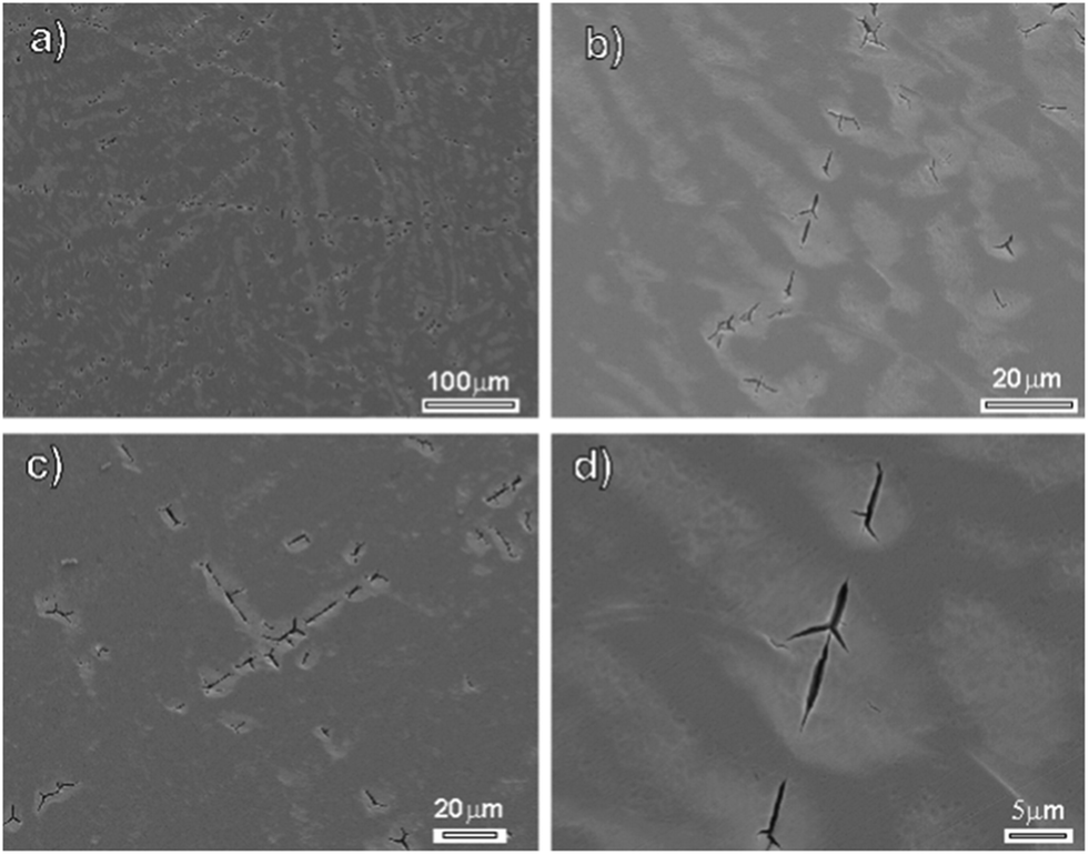 | ||
| Fig. 10 SEM images after dealloying of a Cu3Au polycrystalline surface modified with a self-assembled BT and exchanged with a BSe monolayer. (a)–(d) SEM images of the surface cracks after one CV from −0.2 to 1.0 V vs. Ag/AgCl at 10 mV s−1 in 0.1 M H2SO4. | ||
As reported for Cu and Au, the surface mobility may be orders of magnitude higher in solution (in particular when halides are present) than in vacuum or dry atmospheres.38–41 Smaller structural defects should be removed by gentle chemical annealing in acidic electrolytes but larger polishing scratches will not be removed by this simple method (requires a number of sputter-annealing cycles in UHV). Using such a surface with still present scratches, however, allows in parallel to follow the effect of such macroscopic defects on the dealloying behavior. Although a slight increase of dealloying probability is visible, the density and size of the dealloyed sites are not largely influenced by these defects. But higher numbers of cracks are clearly visible along such polishing lines. Also, the cracks follow mostly the direction of the defect or polishing lines. Macroscopic structural defects thus do clearly influence the stability of our chosen model system, Cu3Au, during dealloying.
Conclusion
The conclusions that are derived for the current study are as follows:➢ In situ AFM studies of dealloying corrosion of surfaces modified with a micro-structured inhibitor pattern applied by μ-contact printing is a promising approach to study the effect of inhomogeneous organic molecular films.
➢ Even a small density of hexadecanethiol SAMs molecules can suppress the typical Au island formation on Cu3Au (111) at intermediate potentials.
➢ This study also shows the potential dependent mobility of thiol islands. Diffusion of hexadecanethiol molecules can take place at elevated potentials.
➢ Only at higher potentials, dealloying initiates at the areas with the lowest concentration of thiol.
➢ The local dealloying pattern is highly influenced and controlled by a molecular exchange of thiols to selenols and is also affected by introducing structural defects such as scratches or polishing defects (lines).
References
- M. Finsgar and J. Jackson, Corros. Sci., 2014, 86, 17–41 CrossRef CAS PubMed.
- Y. Chen, Z. Xu, C. Smith and J. Sankar, Acta Biomater., 2014, 10, 4561–4573 CrossRef CAS PubMed.
- R. A. Antunes and M. C. Lopes de Oliveira, Acta Biomater., 2012, 8, 937–962 CrossRef CAS PubMed.
- H. H. Uhlig, Uhlig’s Corrosion Handbook, 3rd edn, ed. R. W. Revie, John Wiley & Sons, Inc., Hoboken, NJ, USA, 2011 Search PubMed.
- E. E. Oguzie, C. B. Adindu, C. K. Enenebeaku, C. E. Ogukwe, M. A. Chidiebere and K. L. Oguzie, J. Phys. Chem. C, 2012, 116, 13603–13615 CAS.
- J. Denayer, J. Delhalle and Z. Mekhalif, J. Electroanal. Chem., 2009, 637, 43–49 CrossRef CAS PubMed.
- G. Fonder, J. Delhalle and Z. Mekhalif, Appl. Surf. Sci., 2010, 256, 2968–2973 CrossRef CAS PubMed.
- P. E. Laibinis and G. M. Whitesides, J. Am. Chem. Soc., 1992, 114, 9022–9028 CrossRef CAS.
- G. K. Jennings, J. C. Munro, T. H. Yong and P. E. Laibinis, Langmuir, 1998, 14, 6130–6139 CrossRef CAS.
- S. Hosseinpour, M. Gothelid, C. Leygraf and C. M. Johnson, J. Electrochem. Soc., 2014, 161, C50–C56 CrossRef CAS PubMed.
- J. C. Love, L. A. Estroff, J. K. Kriebel, R. G. Nuzzo and G. M. Whitesides, Chem. Rev., 2005, 105, 1103–1169 CrossRef CAS PubMed.
- F. Schreiber, Prog. Surf. Sci., 2000, 65, 151–256 CrossRef CAS.
- J. C. Love, D. B. Wolfe, R. Haasch, M. L. Chabinyc, K. E. Paul, G. M. Whitesides and R. G. Nuzzo, J. Am. Chem. Soc., 2003, 125, 2597–2609 CrossRef CAS PubMed.
- A. Bashir, D. Kaefer, J. Mueller, C. Woell, A. Terfort and G. Witte, Angew. Chem., Int. Ed., 2008, 47, 5250–5252 CrossRef CAS PubMed.
- J. V. B. J. A. Martínez, R. C. Milánc, J. Herrera, M. H. Farías and M. P. Hernández, Appl. Phys. Lett., 2014, 320, 287–293 Search PubMed.
- C. Vericat, M. E. Vela, G. A. Andreasen, R. C. Salvarezza, F. Borgatti, R. Felici, T. L. Lee, F. Renner, J. Zegenhagen and J. A. Martin-Gago, Phys. Rev. Lett., 2003, 90, 075505 CrossRef.
- J. Jia, A. Bendounan, H. M. N. Kotresh, K. Chaouchi, F. Sirotti, S. Sampath and V. A. Esaulov, J. Phys. Chem. C, 2013, 117, 9835–9842 CAS.
- K. Szelagowska-Kunstman, P. Cyganik, B. Schuepbach and A. Terfort, Phys. Chem. Chem. Phys., 2010, 12, 4400–4406 RSC.
- W. Azzam, A. Bashir, A. Terfort, T. Strunskus and C. Woll, Langmuir, 2006, 22, 3647–3655 CrossRef CAS PubMed.
- F. U. Renner, A. Stierle, H. Dosch, D. M. Kolb, T. L. Lee and J. Zegenhagen, Nature, 2006, 439, 707–710 CrossRef CAS PubMed.
- F. U. Renner, A. Stierle, H. Dosch, D. M. Kolb, T. L. Lee and J. Zegenhagen, Phys. Rev. B: Condens. Matter Mater. Phys., 2008, 77, 235433 CrossRef.
- J. Erlebacher, M. J. Aziz, A. Karma, N. Dimitrov and K. Sieradzki, Nature, 2001, 410, 450–453 CrossRef CAS PubMed.
- A. Pareek, S. Borodin, A. Bashir, G. N. Ankah, P. Keil, G. A. Eckstein, M. Rohwerder, M. Stratmann, Y. Gruender and F. U. Renner, J. Am. Chem. Soc., 2011, 133, 18264–18271 CrossRef CAS PubMed.
- A. Pareek, G. N. Ankah, S. Cherevko, P. Ebbinghaus, K. J. J. Mayrhofer, A. Erbe and F. U. Renner, RSC Adv., 2013, 3, 6586–6595 RSC.
- G. N. Ankah, A. Pareek, S. Cherevko, J. Zegenhagen and F. U. Renner, Electrochim. Acta, 2014, 140, 352–358 CrossRef CAS PubMed.
- F. U. Renner, A. Bashir, G. N. Ankah, B. R. Shrestha, D. Ma, P. Losada-Pérez, M. J. Duarte, M. Nellessen, A. Khorashadizadeh, P. U. Biedermann, D. Raabe and M. Valtiner, Star-shaped crystallographic cracking of localized nanoporous defects, submitted.
- T. P. Moffat, F. R. F. Fan and A. J. Bard, J. Electrochem. Soc., 1991, 138, 3224–3235 CrossRef CAS PubMed.
- S. Parida, D. Kramer, C. A. Volkert, H. Roesner, J. Erlebacher and J. Weissmueller, Phys. Rev. Lett., 2006, 97, 035504 CrossRef CAS.
- A. Kumar and G. M. Whitesides, Appl. Phys. Lett., 1993, 63, 2002–2004 CrossRef CAS PubMed.
- J. L. Wilbur, A. Kumar, H. A. Biebuyck, E. Kim and G. M. Whitesides, Nanotechnology, 1996, 7, 452–457 CrossRef CAS.
- J. Tien, A. Terfort and G. M. Whitesides, Langmuir, 1997, 13, 5349–5355 CrossRef CAS.
- L. Yan, C. Marzolin, A. Terfort and G. M. Whitesides, Langmuir, 1997, 13, 6704–6712 CrossRef CAS.
- L. Yan, X. M. Zhao and G. M. Whitesides, J. Am. Chem. Soc., 1998, 120, 6179–6180 CrossRef CAS.
- A. W. Hassel, K. Fushimi and M. Seo, Electrochem. Commun., 1999, 1, 180–183 CrossRef CAS.
- W. Azzam, A. Bashir, P. U. Biedermann and M. Rohwerder, Langmuir, 2012, 28, 10192–10208 CrossRef CAS PubMed.
- G. N. Ankah, S. Meimandi and F. U. Renner, J. Electrochem. Soc., 2013, 160, C390–C395 CrossRef CAS PubMed.
- D. Kaefer, A. Bashir and G. Witte, J. Phys. Chem. C, 2007, 111, 10546–10551 CAS.
- J. Wiechers, T. Twomey, D. M. Kolb and R. J. Behm, J. Electroanal. Chem., 1988, 248, 451–460 CrossRef CAS.
- C. Alonso, R. C. Salvarezza, J. M. Vara and A. J. Arvia, Electrochim. Acta, 1990, 35, 1331–1336 CrossRef CAS.
- M. Giesen and D. M. Kolb, Surf. Sci., 2000, 468, 149–164 CrossRef CAS.
- M. Giesen, Prog. Surf. Sci., 2001, 68, 1–153 CrossRef CAS.
| This journal is © The Royal Society of Chemistry 2015 |