 Open Access Article
 This Open Access Article is licensed under a Creative Commons Attribution-Non Commercial 3.0 Unported Licence
Identification of bulk oxide defects in an electrochemical environment
Mira
Todorova
* and
Jörg
Neugebauer
Max-Planck-Institut für Eisenforschung GmbH, Department for Computational Materials Science, Max-Planck-Str. 1, D-40237 Düsseldorf, Germany. E-mail: m.todorova@mpie.de
First published on 12th January 2015
Abstract
We discuss how electronic-structure calculations can be used to identify the dominant point defects that control the growth and dissolution of the oxide barrier layer formed if a metal comes into contact with a corrosive environment. Using the example of the Zn/ZnO/H2O interface we develop and apply a theoretical approach that is firmly based on ab initio computed defect formation energies and that unifies concepts of semiconductor defect chemistry with electrochemical concepts. Employing this approach we find that the commonly invoked and chemically intuitive defects such as the doubly negatively charged oxygen vacancy in electrochemically formed ZnO films may not be present. Rather, hitherto not discussed defects such as the oxygen interstitial or unexpected charge states, such as the neutral oxygen vacancy, are found. These new defect types will be shown to critically impact our understanding of fundamental corrosion mechanisms and to provide new insight into strategies to develop alloys with higher corrosion resistance.
I. Introduction
Considering the omnipresent oxidising environment it is hard to believe that metals play such an important role in our society. What makes the application of these materials possible is the formation of thin oxide layers at the metal surface, which dramatically enhance their corrosion resistance. Thus, it is not surprising that passivity of metals is a central topic in corrosion science and that the modelling of oxide growth is a major issue. The growth of the oxide layer, the dissolution of the oxide film and the precipitation of dissolving species from solution have been identified as the key phenomena involved in the formation of oxide films.1Understanding the stability and growth kinetics of oxide films requires a detailed knowledge of conditions, with which the metal/oxide/water-system is confronted, i.e., of the involved species and of their transport mechanisms. Since the appearance of Wagner's theory2 on oxide growth considerable effort has been made to understand the elementary processes and the role of point defects (both vacancies and interstitials) in the growth of oxide films. The main models are based on this theory2 and apply to different modes of oxide film growth: the Cabrera–Mott3 and the Fehlner–Mott4 models were developed to treat oxide films formed thermally in air, while the Point Defect Model5 (PDM) was developed for electrochemically formed oxide films. Newer models involve explicit atomistic kinetic Monte Carlo simulations of the oxide growth6 or try to improve on the description of the interfacial potential drops.1 These models are critically reviewed, for example, in ref. 1.
A central input quantity, essential for all of these models, is the thermodynamic and kinetic behaviour of point defects. To be more specific, knowing what kind of defects are present in the oxide in appreciable concentrations for a given electrochemical environment is critical to understand the growth/dissolution of the protective oxide film. In semiconductor defect chemistry, where essentially identical point defect properties are considered and studied, quantum-mechanical calculations based on density functional theory (DFT) have evolved into an indispensable tool to accurately predict the thermodynamic stability and diffusion barriers of neutral and charged point defects in a wide range of semiconductors, including oxides.
Despite addressing principally identical questions the two research fields of semiconductor defect physics and electrochemistry/corrosion are almost disconnected. In this work we discuss how the information about charged point defects in oxides, obtained by concepts originally developed by semiconductor physicists, can be used to obtain a detailed insight into the type and concentration of defects present in an oxide under corrosive conditions. Our approach is based on a grand canonical description of all elementary building blocks involved in the reactions, such as various charged point defects, complexes with extrinsic defects, electrons and holes, and unifies concepts in semiconductor physics and electrochemistry.7 Some of its aspects, relevant in the context of the present work, will be briefly recapped in the next section of this manuscript. Focusing on the Zn/ZnO/H2O system we use these concepts to construct a novel type of phase diagram that directly show the dominant defects as well as the stability of the oxide against dissolution. In Section III we discuss how such defect stability phase diagrams can be utilised to identify which point defects will be important in the context of corrosion and oxide film growth.
II. Theory
A. Point defects in oxide growth models
Passive films are considered to consist of an inner compact oxide layer and an outer precipitated layer.8 The compact layer is supposed to be a native oxide of the material, while the outer layer is assumed to be a mixture of oxide and hydroxide, as discussed for the case of Zn in ref. 8. In this work we focus on the native oxide of Zn, which is ZnO, and its native defects.Before discussing which point defects are commonly assumed to control oxide growth, we would like to comment on our notation, which resembles that used in semiconductor defect chemistry, but is distinct from the Kröger–Vink9 notation typically used in discussions on oxide films. Our notation resembles the Kröger–Vink notation in as far as possible point defects are represented in both of them in the following way: a Zn vacancy is VZn, a Zn interstitial is Zni and an antiside defect, for example a zinc on an oxygen lattice site, is ZnO. Each of these defects D can occur in a charge state q. In the historical Kröger–Vink9 notation a neutral charge state is indicated by a superscript ×, a negative charge state by a superscript ′ and a positive charge state by a superscript ●. In this work we denote the charge state q of the defect Dq as q = 0 for a neutral defect; as q = +1, if one electron is removed; and as q = −1, if one electron is added, following the nomenclature developed in semiconductor defect chemistry.10
Traditionally, defects in oxides are expressed in terms of full or half reactions that individually obey conservation laws with respect to the atomic sites (in solids), numbers and charges. From a historic perspective this approach is convenient to describe and analyse experimental electrochemical set-ups. However, using quantum chemical approaches to describe such reactions is computationally expensive: large cells and time scales are needed, while the number of possible reactions scales approximately as the square of the involved reaction educts and products. We will therefore use a grand canonical approach,10,11 as in semiconductor physics. The approach is based on the calculation of individual defects and the conservation laws with respect to electron and particle numbers are realised not by specific reactions, but by abstract thermodynamic reservoirs for the electrons and the relevant chemical species. These reservoirs are described by chemical potentials for the atomic species and the Fermi energy for the electrons.
The above approach allows an efficient decomposition of the realistic system we are eventually interested in, and which typically contains a variety of defect species in different charge states that interact electrostatically, via charge transfer and by mass transport, into the most fundamental building blocks that can be straightforwardly handled by modern ab initio techniques. This decomposition allows us to focus on the properties of individual defects and only put them into relation with each other a posteriori within the context of a grand canonical formulation, as will be shown later. The main advantage is that we do not have to formulate all possible individual reactions that obey the conservation laws but only the reaction of each individual defect with its thermodynamic reservoirs. The conservation laws need then only be enforced on the total system containing all the defects by modifying/controlling the thermodynamic reservoirs for the various chemical species and the electrons. Due to this the number of calculations scales only linearly with the number of involved defects, rather than with the square we would need if we describe it in terms of charge neutral reactions. The full approach will be outlined in detail in the next section.
Before introducing and applying the above formalism to the Zn/ZnO/H2O system let us briefly recap our present understanding about which point defects participate in the oxide growth.5,8 The assumed relevant defects are summarized in Fig. 1 (left). Following the conventional picture a doubly positively charged oxygen vacancy and a zinc interstitial defect, which may assume different charge states, are dominant at the Zn/ZnO interface, while a negatively charged zinc vacancy is prevalent at the ZnO/H2O interface. Under oxidizing conditions, the interface is far away from thermodynamic equilibrium implying that there will be a substantial gradient in the O and Zn chemical potentials. The schematic behaviour of the two chemical potentials, which are Zn-rich at the Zn/ZnO interface and more O-rich at the ZnO/H2O interface, are included in Fig. 1 (left). Due to the gradient in the chemical potentials defects with a net Zn (O) excess will move towards more oxygen (zinc) rich conditions, i.e. towards the ZnO/H2O (Zn/ZnO) interface. The arrows attached to each of the defects indicate the corresponding migration direction.
 | ||
| Fig. 1 Schematic representation of the Zn/ZnO/H2O system and the defects commonly assumed to be involved in the growth of a compact oxide layer during corrosion. Also schematically shown are the chemical potential (solid and dashed blue lines). (a) Conventional picture: positively charged oxygen vacancies and Zn interstitials are assumed to be created in the vicinity of the Zn/ZnO interface and transported towards the ZnO/(H2O/outer layer) interface; negatively charged Zn vacancies are generated in the vicinity of the ZnO/(H2O/outer layer) interface and transported through the compact oxide layer towards the Zn/ZnO interface. (b) Revised picture derived in Sec. III based on DFT-calculated defect formation energies: neutral oxygen vacancies are generated in the vicinity of the Zn/ZnO interface and transported towards the ZnO/(H2O/outer layer) interface; doubly negatively charged Zn vacancies and neutral O interstitials are generated in the vicinity of the ZnO/(H2O/outer layer) interface and transported through the compact oxide layer towards the Zn/ZnO interface. | ||
Fig. 1 (right) is based on the insight we gain from the grand canonical approach and will be discussed in Section III.C.
B. Defect formation energies and chemical potentials
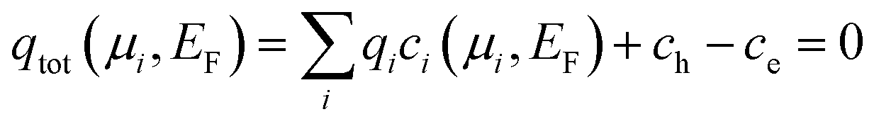
The formal equivalency between defects in semiconductors and ions in solution allows us to extend concepts typically used to study charged point defects in semiconductors to electrochemical systems.7 As discussed in Section II.A, the derived grand-canonical approach is particularly well suited to be used in conjunction with ab initio calculations, since it needs as input only the properties of the individual charged defects within a system and couples them only afterwards via the conditions of charge neutrality. Besides providing information on the stability and concentration of ions in solution, the approach we are going to describe in the following provides a natural link between density-functional theory calculations and experimentally measurable quantities, which determine and characterize the state of electrochemical systems, such as pH and electrode potential. In the following we recap some of the concepts, in particular the ones pertaining to defects in oxides, which become important in the context of the later discussion.A key quantity to describe oxide growth is the local concentration of the various point defects. Assuming local thermodynamic equilibrium, i.e., the defect concentration is in thermodynamic equilibrium with its local chemical potential, and the dilute limit where defect–defect interactions are negligible,12 the concentration of a defect D in charge state q is given by:
| cDq = c0e−ΔfG(Dq)/kBT | (1) |
Quantities that enter eqn (1) are c0, the highest possible concentration which can be realised within the system by occupying every available site where the defect can be formed, the Boltzmann constant kB, the temperature T, and the free energy of formation of a charged defect in a semiconductor or an ion in solution ΔfG(Dq). The above equation implies that defects with a high free energy of formation will be present only in small concentrations, while defects with low formation energies will occur in high(er) concentrations. The free energy of formation itself is given by the change in enthalpy ΔfH and entropy ΔfS. Since the formation of the defect/ion requires an exchange of Δni atoms and q electrons with their respective thermodynamic reservoirs, the formation energy becomes a function of chemical potentials μi and Fermi energy μe:7,11
 | (2) |
 | (3) |
In a first step, the chemical potentials of the electrons μe (or Fermi energy EF) and of the chemical species μi are treated as variables. They can be used to analyse the influence of the electrochemical environment (chemical potentials, overpotential, pH) on the defect formation energy and concentrations. Due to thermodynamic/electronic constraints the electron and chemical potentials are restricted by upper and lower bounds.
For example, the electron chemical potential μe can assume within the oxide only values within the electronic band gap, i.e. the lower (upper) boundary for the electron potential μe is the valence band maximum (VBM) [conduction band minimum (CBM)]. For the chemical potentials of the involved species boundaries exist, if the considered oxide becomes unstable against the formation of another phase. A natural upper boundary for any species is the formation of its elemental state: for ZnO, consisting of Zn and O, this would be bulk fcc Zn and O2 molecules, respectively. Since potentials are invariant against a constant shift for convenience the energy zero of the chemical potentials is commonly chosen such that the chemical potential of the elementary phase becomes zero. Thus, a general upper limit is μi ≤ 0.
While the formation of the elementary phases is an upper limit it is not always the lowest and thus critical one. Often the formation of (parasitic) phases sets in before the elemental phase can be formed. For the system discussed here, where the three chemical elements Zn, O, H are present, a possible parasitic phase is Zn(OH)2. Then the resulting boundary conditions is, for example for Zn, μZn ≤ ΔfH(Zn(OH)2) − 2μO − 2μH.
Finally, the chemical potentials are not independent but linearly dependent on each other in a way that ensures thermodynamic stability of the involved phases. To be more specific we consider ZnO, where the two relevant chemical potentials are μZn and μO. In thermodynamic equilibrium these two chemical potentials cannot be varied independently from each other. They are bound by the condition that ZnO must be a stable phase, which means that the stoichiometric sum of μZn and μO must be equal to the enthalpy of formation of the compound,
| μO + μZn = ΔfH(ZnO). | (4) |
C. Electron potential
While the definition and calculation of an absolute alignment (energy zero) for the chemical potentials is straightforward and easily achieved, e.g., by referencing all chemical potentials with respect to that of the corresponding elementary phases (see discussion above) the definition of an absolute potential for the electron reservoir is conceptually much less straightforward. In the semiconductor community the Fermi energy describing this potential is commonly referenced to the top of the valence band. While this is sufficient to describe, e.g., optical transitions or doping within a given bulk system it does not allow to compare the formation energy between two or more separate bulk systems as e.g. ZnO and water. A common absolute reference is the vacuum level in semiconductor physics or the standard hydrogen electrode (SHE) employed in electrochemistry. How the energy of these two references can be related has been discussed in detail by Trasatti13 and in a recent publication by us.7 In the following we use the notation μe whenever we want to indicate alignment on an absolute energy scale and EF when we utilize formation energies computed by the semiconductor community where the alignment is with respect to the VBM.D. Computational details
In order to utilize the above described formalism the needed key input quantities are the defect formation energies defined by eqn (3). These require calculations of the total energies for the perfect bulk system (the host) and of the possible defects in all relevant charge states. Additionally, to obtain the alignment in the chemical potentials described above the total energy Ephase,itot of the elementary phases of each involved species i is needed to get the chemical potentials entering eqn (3):| μi = μalignedi − Ephase,itot | (5) |
Since the focus of the present paper is to show how the techniques and data produced in the semiconductor community can be used in the context of wet corrosion and oxide film formation we refrain from re-computing defect formation energies whenever such data exist in the literature. Thus, in the following we show and discuss how existing data on defect formation energies can be used in the context of corrosion and oxide growth.
Over the last few years ZnO has received a lot of attention in the semiconductor community due to its potential as a direct wide bandgap semiconductor for optoelectronic, as well as, electronic devices. Since for such devices doping and compensation by native defects is a fundamental aspect a large number of very detailed ab initio studies on the energetics and electronic structure of point defects have been reported in the literature. The actual calculation of accurate defect formation energies is challenging due to the bandgap problem encountered by the conventionally employed semilocal DFT xc functionals, finite size effects of the employed periodic supercells (particularly for charged defects) or band alignment, to name only a few.11 Recently developed hybrid functionals such as HSE,14 which mix in a certain amount of exact-exchanged, allow the bandgap problem to be overcome and provide at the same time total energy capabilities important to compute the equilibrium configurations of the defects, including atomic relaxation. Various correction schemes to treat charged defects11,15–17 allow to reduce largely finite size effects and obtain the accurate dilute limit even with rather modest supercell sizes in the order of 100 atoms.
Specifically, for ZnO we will use the formation energies computed by Oba et al.18 which have been obtained using HSE and charge corrections. Since the oxygen interstitial defect has not been considered in ref. 18 we also use formation energies computed by Janotti et al.19
As shown by several studies, employing HSE leads to a dramatic improvement in the description of metal oxide compound properties.20 To improve the accuracy of semiconductor defect calculations in many HSE studies the mixing parameter between the use of non-local Fock-exchange and the semilocal DFT functional is not 0.25 as suggested in the original formulation14 but adapted to provide an optimal (but material specific) value. For ZnO, values significantly larger than 0.25 have been used: in the calculations of Oba et al.18α = 0.375 is used, while the calculations of Janotti et al.19,21 are performed using α = 0.36. Both choices improve the description of the position of the 3d Zn states, the band gap, the lattice parameters and the heat of formation ΔfH compared to experiment, resulting in an equally satisfying description, as can be seen in Table 1.
| α = 0.375 | α = 0.36 | Experiment | |
|---|---|---|---|
| a (Å) | 3.25 | 3.25 | 3.25 |
| c (Å) | 5.20 | 5.26 | 5.21 |
| ΔfH (eV) | −3.13 | −3.43 | −3.63 |
| E gap (eV) | 3.43 | 3.29 | 3.44 |
Taking the defect formation energies from ref. [18, 19 and 21] and plugging them into eqn (3) we obtain for any defect and charge state its formation energy as a function of the Fermi energy and the chemical potentials. As outlined in the previous subsection we have to consider only one chemical potential (we chose here the oxygen one). Following the conventions in the semiconductor community these energies are plotted as function of the Fermi energy and for a fixed chemical potential. The results for the two extreme conditions of the chemical potentials, i.e., O-rich and Zn-rich, are shown in Fig. 2.
 | ||
Fig. 2 Formation energies of native point defects of ZnO shown as a function of Fermi-level position for Zn-rich (right) and O-rich (left) conditions. Only segments corresponding to the lowest energy charge states for each defect are shown. The coloured areas depict the regions where the given defect species dominates. The zero on the Fermi-level EF-axis corresponds to the VBM (valence band maximum). The slope of each line corresponds to the respective charged state. The ab initio calculated defect formation energies used to construct these diagrams were taken from ref. 18. The dashed-lines marked “(JVdW)” [ and Oi (split)] are constructed using HSE-data obtained by Janotti and Van de Walle.19,21 and Oi (split)] are constructed using HSE-data obtained by Janotti and Van de Walle.19,21 | ||
Analyzing these diagrams provides important insight into which defects dominate, into their electronic behaviour, i.e., do they accept or donate electrons, as well as their possible charge states. The defect with the lowest formation energy for a given set of chemical potentials and Fermi level will be the dominant one and occur in much higher concentrations than all other defects. For O-rich conditions Fig. 2a shows that under p-type conditions (i.e. for Fermi energies close to the valence band) a ZnO antisite in a 4+ charge state is dominant. Going towards higher Fermi levels (above 0.6 eV) the oxygen vacancy in a 2+ charge state, and above EF = 2.2 eV the neutral oxygen vacancy, become the dominant defects. Under Zn-rich conditions and going from p to n-type conditions first the oxygen 2+ vacancy, then a neutral oxygen (split) interstitial and a 2+ Zn vacancy are stable.
While the 2+ oxygen and 2− zinc vacancy are chemically intuitive and invoked in the conventional picture (see Fig. 1a) the previously postulated Zn interstitial is absent, while neutral defects (such as the oxygen vacancy or the oxygen split interstitial) or a charged defect, such as the ZnO antisite, have never been considered. Whether these defects become important under realistic electrochemical conditions will be discussed in Sec. III.
E. Defect transition levels and charge neutrality
An important benefit of representing defect formation energies in a diagram such as Fig. 2 is that the diagram provides direct insight into which defects are the thermodynamically most stable ones, thus allowing us to derive phase diagrams. It also provides direct insight into the electronic behaviour of any given defect by giving the possible charge states (oxidation states), as well as, the position of the Fermi level where the transition from one state into the other occurs, i.e., the transition (redox) levels in the electronic bandgap.To derive this information we note that the slope of the defect formation energies in Fig. 2 is according to eqn (3) the charge q of the defect: the position of the Fermi energy EF enters only the last term qEF. Consequently, the slope of the formation energy gives the charge (oxidation) state the defect has at a given Fermi level while the kinks in the formation energy imply a change in the charge state, thus giving the position of the transition level. Therefore, diagrams such as Fig. 2, which have been computed for a large number of bulk semiconductor/oxide materials and have been reported in the literature, can be used directly to extract all relevant defect properties for a given system.
We note that the actual numbers depend sensitively on the chosen xc functional as well as on the level of convergence. In fact, for well-studied semiconductor systems such as, e.g., GaAs several sets of ab initio calculations exist that give differences of several eV(!) for the same defect. It is therefore of paramount importance when using existing literature data to carefully check that they are based on state-of-the-art hybrid xc functionals, include charge corrections and are well converged (e.g. with respect to supercell size, k-point sampling, etc.).
Fig. 2 shows nicely that state-of-the-art defect calculations have reached a maturity giving, if properly applied, essentially identical results. This can be seen for the example of the Zn vacancy for which an independent calculation by Janotti et al.21 has been reported in the literature and marked as JVdW (dashed red line) in Fig. 2. Since in this study the authors focused on the technologically relevant case of n-type conditions where the 2+ charge state is the most stable one, the comparison is possible only for this charge state. An almost perfect match with a deviation of less than 0.1 eV is found. This level of agreement allows us to include in our considerations the O interstitial computed by the same group and which has not been considered in the original study of Oba et al.18
Having the energetic and electronic properties of all individual defects as a function of chemical potentials and Fermi level allows us to construct the full picture of a realistic system consisting of a variety of defects. For the following discussions we assume that all defects are in the dilute limit, i.e., their concentration is so low that direct defect–defect interaction can be neglected. For the system considered here, ZnO and water, defect/ion concentrations are expected to be well below 1%, so that this assumption should be well justified.
While in the dilute limit a direct interaction between the defects can be safely excluded, an interaction with the chemical and electron reservoir occurs and has to be included. To be more specific let us first focus on the interaction with the electron reservoir. To realize a specific charge state q the defect has to exchange electrons with the electron reservoir. For example, to create the 2+ oxygen vacancy the defect has to transfer two electrons to the Fermi reservoir while creating a Zn 2− vacancy requires the transfer of two electrons from the reservoir to the defect. An important condition for any system is that it must be neutrally charged. In the grand canonical concept of an electron reservoir this simply means that the number of electrons transferred to the reservoir must be identical to the number of electrons taken out, i.e., in the charge neutral case the reservoir will be completely empty and all transferred electrons will be distributed over the defects.
Formally, the above condition of charge neutrality can be expressed as follows:7,11
 | (6) |
An important advantage of this approach is that we do not need to start from individual charge neutral reactions as commonly performed when describing electrochemical reactions. Rather, all conceivable reactions are intrinsically included in eqn (6). This equation thus provides the formal justification (i) why complex electrochemical systems can be decomposed into isolated non-charge neutral non-stoichiometric defects, that can be treated separately and (ii) that interact/couple only via their respective chemical/electronic reservoirs.
III. Discussion
A. Point defect stability phase diagrams
As discussed in the last section, in the field of semiconductor defect chemistry point defect formation energies are usually evaluated and discussed within plots such as the ones shown in Fig. 2. A disadvantage of these plots is that for each set of chemical potentials a separate plot is needed. For example, the phase diagrams shown in Fig. 2a and b strictly apply only for extreme Zn-rich and O-rich conditions implying that under intermediate conditions other defects may become most stable. Extending the concept of Pourbaix-diagrams which are a well-established concept in electrochemistry, showing the most stable bulk and defect (i.e. ions in water or other solvents) phases as function of pH and overpotential, we recently proposed a schema to construct defect phase diagrams that span the full configuration space as defined by the relevant chemical potentials and the chemical potential of the electron.7,23 The key idea is to replace the pH value, which is a function of the oxygen chemical potential and the overpotential, by the oxygen chemical potential via a Legendre transformation. Using eqn (3) we can identify for any set of chemical potential(s) and overpotential the defect (i.e. type and charge state) with the lowest formation energy and thus directly construct such a phase diagram. For ZnO such a defect phase diagram is shown in Fig. 3 and yields for any thermodynamically allowed combination of oxygen chemical potential and overpotential, the dominant defect.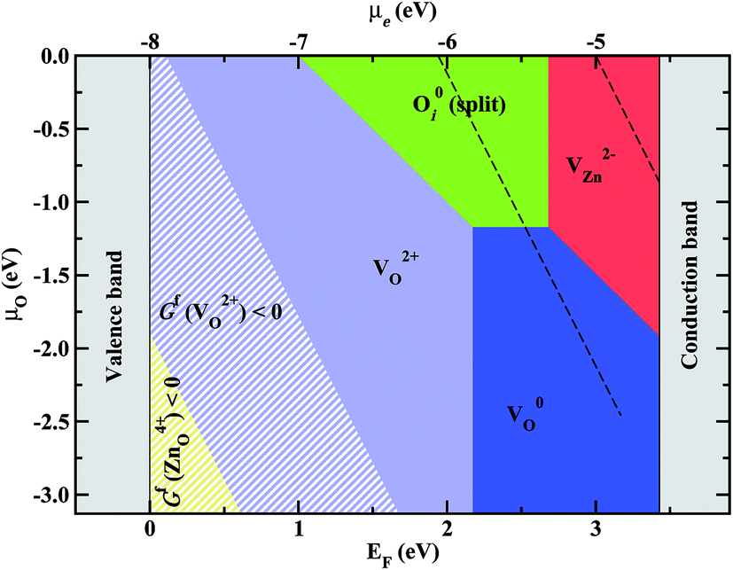 | ||
| Fig. 3 Defect stability phase diagram for ZnO showing the regions where the respective native point defects dominate. Striped areas correspond to regions where ZnO becomes thermodynamically unstable against the formation of the respective point defects having negative formation energy in this region. The zero energy on the EF-axis corresponds to the VBM. The μe-axis shows the electrode potential on an absolute scale. The black dashed-lines mark the boundaries of the electrochemical stability window of water. | ||
As mentioned in Section II.C, in electrochemistry the absolute value of the Fermi level μe rather than the relative level EF with respect to the top of the valence band is the relevant one. To align the two levels we utilise the universal alignment of the H+/H− transition level observed in semiconductors, insulators and water.24 The absolute level is shown on the upper x-axis both in Fig. 2 and 3.
As seen in Fig. 3, the set of defects that can become stable in ZnO is identical to the one identified from Fig. 2 considering only extreme Zn and O rich conditions. However, as becomes obvious also from Fig. 3 the region of Fermi levels where the respective defect becomes the dominant one strongly depends on the specific environment (oxygen chemical potential μO).
Since Fig. 3 is formally equivalent to a Pourbaix diagram we can immediately superimpose the well-known region of water stability, bounded in Fig. 3 by the two dashed black lines. The upper-right/lower-left line gives the boundary towards water becoming thermodynamically unstable against H2/O2 formation.
An important insight we gain from Fig. 3 is that in a substantial region defect formation energies become negative, i.e., the formation of defects is exothermic implying that the oxide becomes unstable at these conditions. It is interesting to note that this instability of an oxide against exothermic formation of point defects is equivalent to the well-known water instability where the formation of the “intrinsic point defects” (solvated H+ and OH−) becomes exothermic. The regions, where ZnO becomes unstable, as a result of the negative defect formation energies of 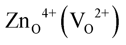 are marked in Fig. 3 as hashed yellow (blue) areas. The fact that the system always becomes unstable against defect formation under extreme p-type conditions (i.e. independent of the choice of the chemical potentials) may explain why p-type conductivity remains elusive in ZnO.
B. Fermi energy position within the zinc/ZnO/water system
To connect the defect phase diagram (Fig. 3) with the oxide passivation layer bounded by Zn-bulk and water we need to know the position of the Fermi level as well as of the oxygen chemical potentials as a function of distance to the respective interfaces. To estimate the position of the Fermi level within the oxide film we first align the band structures of Zn, ZnO and H2O with respect to the vacuum level. This is shown in Fig. 4, where we use the work function of zinc [Φ = 4.3 eV (ref. 25)] (which is by definition the Fermi energy position with respect to the vacuum level). For ZnO and water we use the universal alignment approach24 mentioned previously.7,26 For ZnO we assume n-type conditions to be consistent with experimental observations.8,27,28 | ||
| Fig. 4 Diagram showing the alignment of bands within the Zn/ZnO/water system (a) before equilibration and (b) after equilibration. The red dashed-line in (b) marks the position of the Fermi-energy level within the equilibrated system. The energy region within which the water Fermi-energy can be varied is marked by blue-striped regions depicting the extremes of possible chemical potential conditions which are H-rich and O-rich. For further details see text. | ||
Fig. 4(a) shows the alignment before the systems come into contact, i.e., before electronic charge transfer occurs. Fig. 4(b) shows schematically the alignment after electronic charge transfer which results in a constant and identical Fermi level throughout the system. Since both the metal and water have an infinitely higher propensity to screen charges compared to a semiconductor, the potential drop at the Zn/ZnO and at the ZnO/H2O interfaces will occur on the ZnO side of the respective interfaces,29,30 leading to the formation of a space-charge layer and band bending. Since the Fermi energy of zinc lies above the CBM of ZnO there will be a flow of electrons from the metal to the conduction band of the oxide. As a consequence in this region the Fermi level will be above the conduction band, resulting in excess electrons forming a 2-dimensional electron gas (2DEG) and driving the system to extreme n-type conditions.
The Fermi level at the Zn/ZnO interface is pinned by the metal and cannot be changed. The opposite interface is formed by water for which the position of the Fermi level is not a constant but varies depending on the environment (chemical potentials, pH, overpotential). As shown in Fig. 3 the Fermi level cannot be chosen freely but is bounded by the condition of water stability, i.e., that the native defects in water must have an endothermic formation energy. This region of allowed Fermi levels is marked in Fig. 4 by hashed boxes for extreme H-rich and O-rich conditions. As can be seen the region of permitted Fermi levels is restricted to a rather small region in the water band gap. Since the Fermi level in water is variable, the exact shape of the band bending will depend on it. In Fig. 4 we therefore chose an intermediate value for EF to sketch the band bending. Depending on the specific set-up band bending can be positive or negative, i.e., extreme n-type conditions up to semi-insulating conditions may exist at this interface (see Fig. 3).
C. Point defects in the context of barrier oxide growth
We now have all the ingredients needed to identify the defect species that drive oxide growth. Since the two interfaces are chemically very different we start with the Zn/ZnO interface. This interface turns out to be conceptionally simpler since both Fermi level and chemical potential are fixed and well defined. Since the oxide layer is in direct contact with the Zn bulk and the Fermi level is slightly above the top of the conduction band (see Fig. 4b) we identify from the defect phase diagram (Fig. 3) the neutral oxygen vacancy as the most stable defect.This may be surprising in two aspects: first, the oxygen vacancy in the context of oxide growth/corrosion has always been assumed to be 2+ which, however, based on Fig. 3 can be safely excluded. Second, to enable oxide growth defects with excess Zn should move from the Zn-bulk interface to the water interface while O excess defects should move in the opposite direction. Defects with Zn excess are Zn interstitials, Zn antisites and O vacancies and should be preferentially formed at the Zn interface while defects with O excess are O interstitials, O antisites and Zn vacancies that should form at the water interface. Indeed, Fig. 3 shows that at the Zn interface the defect that can be formed most easily, i.e., the one which has the lowest formation energy is the O vacancy. However, Fig. 3 also indicates that when going from Zn-rich towards O-rich conditions the formation energy becomes higher and above a critical value becomes even higher in energy than defects with O excess such as the O interstitial and the Zn vacancy. In other words it looks like the defect would have to go in a direction where its formal formation energy becomes higher, i.e., where the defect becomes energetically less favourable. This apparent discrepancy can be easily resolved by noting that the driving force for defect migration is the gradient in the chemical potential which will only disappear once thermodynamic equilibrium is achieved, i.e., if the gradient vanishes.
Based on Fig. 3 together with the alignment diagram (Fig. 4) we can also identify the dominant defects for the interface of the ZnO with water. Under more oxygen-rich conditions the 2+ Zn vacancy [under n-conditions (μe > −5.3 eV)] and the charge neutral O interstitial [under more electronegative conditions (μe < −5.3 eV)] become the dominant defects. Both are defects with O excess, consistent with our expectations to what defects should be formed at this interface to promote the growth of the oxide film. Under less oxidizing conditions (μO ≤ −1.2 eV) the neutral O vacancy becomes again stable. Since this is an oxygen deficient defect growth of the oxide passivation layer growth is expected to slow down.
The approach outlined in this study provides thus an efficient and physically transparent approach to identify the relevant defects in the passivation layer under realistic electrochemical conditions. The defects identified here, the neutral O vacancy on the Zn interface and the Zn vacancy and O interstitial on the water interface (see Fig. 1b) are rather different compared to the ones assumed in the conventional picture (Fig. 1a). While the expected  is indeed found at the water side our formalism shows that this is true only if the water overpotential is above 0.6 V vs. SHE, otherwise a hitherto not considered O interstitial in a neutral charge state will prevail. For the interface with Zn bulk the expected O vacancy is found to be dominant, however in the neutral not the 2+ charge state.
The identification of neutral rather than of charged defects that drive oxide growth has important consequences. In the conventional picture where transport by a 2+ O vacancy is assumed two criteria apply to activate this mechanism: (i) formation energy and diffusion barrier for the O vacancy have to be sufficiently low to enable diffusion at operating temperatures and (ii) electrons must be sufficiently mobile to ensure local charge neutrality. If electron transport for a given system is inefficient or negligible (e.g. for highly resistive oxides where the Fermi level is deep in the bandgap) the moving charged defects would quickly built up an energetically costly space charge which would quickly suppress further migration. This well-known concept to improve the corrosion resistance of a material is however counteracted if the materials transport inside the oxide is realized by charge neutral defects. In this case the defect carries its electron with itself. Consequently, making the material more intrinsic by reducing the Fermi level (e.g. by doping) would not slow down the transport. Only if the Fermi level comes into a region of the defect phase diagram where a charged defect becomes dominant the conventional picture would apply again. For the oxide considered here, ZnO, this would be the case if the Fermi level drops by more than 1.5 eV below the conduction band (see Fig. 3). Under realistic conditions it may be difficult/impossible to achieve such extremely intrinsic (resistive) conditions. The methods outlined here would be ideally suited to perform a systematic search for suitable dopants that are able to bring the Fermi level into the desired region and thus to design materials with a higher corrosion resistance.
IV. Summary and conclusions
In the present work we outlined a formalism and strategies that allow us to connect the vast knowledge of intrinsic point defects in semiconductors and particular in oxides acquired over the years with issues relevant in wet corrosion. To demonstrate and discuss this strategy for a specific and technologically relevant example we focus on the growth and stability of the barrier oxide that is formed once Zn comes into contact with a water film. The resulting oxide film, ZnO, is instrumental to e.g. realize the corrosion protection in galvanized steels. At the same time, ZnO has also been a well-studied semiconductor material providing ample defect data. The construction of defect phase diagrams (Fig. 3) turned out to be key in connecting these two very different worlds. These diagrams use as input only defect energies that are often readily available from ab initio calculations reported in the literature and an absolute alignment in the electronic levels as described in ref. 7. Using these phase diagrams allows us to make a direct connection to electrochemistry conditions, e.g., to directly include conditions of water stability. This, together with a careful consideration of band alignments (Fig. 4) makes it possible to identify the relevant defects.Applying this formalism revealed a number of surprises for an, at first glance, extremely well studied oxide such as ZnO: compared to the standard and chemically intuitive picture we find that neutral rather than 2+ charged O vacancies become prevalent or that neutral O interstitials (which have not been considered so far in the context of Zn corrosion) can become the dominant defect species. These findings are not only important because new/different defects compared to the commonly expected ones are observed. Probably even more important is that charge neutral defects become the dominant species under electrochemically relevant conditions. Such defects behave qualitatively different compared to charged ones as outlined in Sec. III.C. As also discussed this insight may be used to identify new strategies towards improving corrosion resistance.
As a last remark we note, that the approach derived and discussed here for the Zn/ZnO/H2O system is general and can be directly employed to other metal/oxide/electrolyte systems as well as for Zn/ZnO/gas systems relevant for high temperature corrosion. We believe, that the insights gained from the strategies and concepts derived in this paper may significantly enhance our understanding on formation and evolution of oxide passive layers on metal surfaces in corrosive environments and help to develop systematic approaches to search for alloys with improved corrosion resistance.
Acknowledgements
We thank A. Janotti and C. G. Van de Walle for providing us with the HSE-calculated formation energy of the O0i (split) interstitial point defect and stimulating discussions. The funding by the European Research Council under the EU's 7th Framework Programme (FP7/2007–2013)/ERC Grant agreement 290998 is gratefully acknowledged. This work is supported by the Cluster of Excellence RESOLV (EXC 1069) funded by the Deutsche Forschungsgemeinschaft.References
- A. Seyeux, V. Maurice and P. Marcus, J. Electrochem. Soc., 2013, 160, C189 CrossRef CAS.
- C. Wagner, Hoppe-Seyler's Z. Physiol. Chem., 1933, 222, 21 CrossRef.
- N. Cabrera and N. F. Mott, Rep. Prog. Phys., 1949, 12, 163 CAS.
- F. P. Fehlner and N. F. Mott, Oxid. Met., 1970, 2, 59 CrossRef CAS.
- D. D. Macdonald, Electrochim. Acta, 2011, 56, 1761 CrossRef CAS.
- B. Diawara, Y. A. Beh and P. Marcus, J. Phys. Chem. C, 2010, 114, 19299 CAS.
- M. Todorova and J. Neugebauer, Phys. Rev. Appl., 2014, 1, 014001 CrossRef.
- S. Thomas, I. S. Cole, M. Sridhar and N. Birbilis, Electrochim. Acta, 2013, 97, 192 CrossRef CAS.
- F. A. Kröger and H. J. Vink, Solid State Phys., 1956, 3, 307 Search PubMed; F. A. Kröger, The Chemistry of Imperfect Crystals, North Holland Publishing Co., Amsterdam, 1974 Search PubMed.
- C. G. Van de Walle and J. Neugebauer, J. Appl. Phys., 2004, 95, 3851 CrossRef CAS.
- C. Freysoldt, B. Grabowski, T. Hickel, J. Neugebauer, G. Kresse, A. Janotti and C. G. Van de Walle, Rev. Mod. Phys., 2014, 86, 253 CrossRef.
- There is no principle difficulty in obtaining concentration dependent free energies of defect formation and an extension of the formalism to such cases is straight forward 7.
- S. Trasatti, Pure Appl. Chem., 1986, 58, 955 CAS.
- J. Heyd, G. E. Scuseria and M. Ernzerhof, J. Chem. Phys., 2003, 118, 8207 CrossRef CAS; J. Heyd, G. E. Scuseria and M. Ernzerhof, J. Chem. Phys., 2006, 124, 219906 CrossRef.
- C. Freysoldt, J. Neugebauer and C. G. van de Walle, Phys. Rev. Lett., 2009, 102, 016402 ( Phys. Status Solidi B , 2011 , 248 , 1067 ) CrossRef PubMed.
- G. Makov, R. Shah and M. C. Payne, Phys. Rev. B: Condens. Matter, 1996, 53, 15513 CrossRef CAS.
- S. Lany and A. Zunger, Phys. Rev. B: Condens. Matter Mater. Phys., 2008, 78, 235104 ( Modell. Simul. Mater. Sci. Eng. , 2009 , 17 , 084002 ) CrossRef.
- F. Oba, A. Togo, I. Tanaka, J. Paier and G. Kresse, Phys. Rev. B: Condens. Matter Mater. Phys., 2008, 77, 245202 CrossRef.
- A. Janotti, Private communication, The HSE-basis set is described in ref. 21.
- A. Janotti, D. Segev and C. G. Van de Walle, Phys. Rev. B: Condens. Matter Mater. Phys., 2006, 74, 045202 CrossRef.
- D. Steiauf, J. L. Lyons, A. Janotti and C. G. Van de Walle, APL Mater., 2014, 2, 096101 CrossRef.
- W. M. Hayness, CRC Handbook of Chemistry and Physics, CRC Press Inc., Boca Raton FL, 95th edn, 2014 Search PubMed.
- M. Todorova and J. Neugebauer, Surf. Sci., 2015, 631, 190–195 CrossRef CAS.
- C. G. van de Walle and J. Neugebauer, Nature, 2003, 423, 626 CrossRef CAS PubMed.
- R. A. Serway and J. W. Jewett, Physics for Scientists and Engineers with Modern Physics, Brooks and Cole, Boston, MA, 2010 Search PubMed.
- J. V. Coe, Int. Rev. Phys. Chem., 2001, 20, 33 CrossRef CAS; J. V. Coe, A. D. Earhart, M. H. Cohen, G. J. Hoffman, H. W. Sarkas and K. H. Bowen, J. Chem. Phys., 1997, 107, 6023 CrossRef.
- A. Janotti and C. G. Van de Walle, Rep. Prog. Phys., 2009, 72, 126501 CrossRef.
- G. Trabanelli, F. Zucchi, G. Brunoro and G. Gilli, Electrodeposition Surf. Treat., 1975, 3, 129 CrossRef CAS.
- H. Gerischer, Electrochim. Acta, 1990, 35, 1677 CrossRef CAS.
- S. Al-Halli and M. Willander, Sensors, 2009, 9, 7445 CrossRef PubMed.
| This journal is © The Royal Society of Chemistry 2015 |