
 Open Access Article
 This Open Access Article is licensed under a
 Creative Commons Attribution 3.0 Unported Licence
Synthesis and controlled growth of osmium nanoparticles by electron irradiation†
Anaïs
Pitto-Barry
 ,
Luis M. A.
Perdigao
,
Marc
Walker
,
James
Lawrence
,
Giovanni
Costantini
*,
Peter J.
Sadler
* and
Nicolas P. E.
Barry
*
,
Luis M. A.
Perdigao
,
Marc
Walker
,
James
Lawrence
,
Giovanni
Costantini
*,
Peter J.
Sadler
* and
Nicolas P. E.
Barry
*
Department of Chemistry, University of Warwick, Coventry CV4 7AL, UK. E-mail: G.Costantini@warwick.ac.uk; P.J.Sadler@warwick.ac.uk; N.Barry@warwick.ac.uk
First published on 29th September 2015
Abstract
We have synthesised osmium nanoparticles of defined size (1.5–50 nm) on a B- and S-doped turbostratic graphitic structure by electron-beam irradiation of an organometallic osmium complex encapsulated in self-spreading polymer micelles, and characterised them by transmission electron microscopy (TEM), high-resolution TEM (HRTEM), and atomic force microscopy (AFM) on the same grid. Oxidation of the osmium nanoparticles after exposure to air was detected by X-ray photoelectron spectroscopy (XPS).
Arrays of metal nanoparticles (MNPs) deposited on surfaces offer much potential for the design of novel nano-materials and exploitation in areas such as catalysis, electronic nanodevices, and quantum computers.1–6 Nanoparticles with diameters of a few nanometers possess electronic properties and atomic structures markedly different from those of the bulk materials, whilst larger nanoparticles (>20–50 nm diameter) are likely to have properties similar to those of the bulk.7 Hence, fine control of the growth and sizes of MNPs during their synthesis is required to allow tuning of their electronic, optical, and magnetic properties as well as chemical characteristics. Although a number of physical (e.g. inert gas condensation,8 laser ablation,9 pyrolysis10) and chemical (e.g. reduction,11 solvothermal12 or electrochemical13) methods for nano-metal deposition have been developed in recent years, it is still challenging to achieve control of the growth and size of nanoparticles over the range from small to large (e.g. 1.5–50 nm).
We recently introduced a new method for the fabrication of small (1 to 2 nm diameter) crystalline MNPs.14,15 Our procedure involved the encapsulation of the organometallic OsII complex [Os(p-cymene)(1,2-dicarba-closo-dodecarborane-1,2-dithiolate)] (1) in the triblock copolymer Pluronic® P12316 to form OsMs micelles (Fig. 1, and ESI†). These micelles contain a defined number of molecules of osmium complex 1,14 and are deformable on surfaces; P123 polymer forms stable Langmuir films at ambient temperature.17 Deposition of aqueous droplets ([OsMs] = 1 mg mL−1) onto lacey carbon-coated TEM grids leads to the formation of an unsupported film over the grid holes. We reported that high-energy electron-beam irradiation of such grids (80 keV; 1.9 pA cm−2) leads to structural changes with the emergence of atomic ordering consistent with a turbostratic graphitic structure in the first few minutes, and a highly-structured few-layer graphene lattice after 50 min of irradiation. Along with these structural modifications of the self-supporting polymeric film, a rapid decomposition of the carborane-containing complex 1 was also observed (in less than one minute), and individual Os atoms could be imaged hopping on the surface, assembling into clusters, and eventually forming nanocrystals with diameters of 1 to 2 nm.14 Electron energy loss spectroscopy (EELS) confirmed the chemical identity of the Os atoms and also suggested that boron and sulfur from the carborane ligand in 1 are present in the turbostratic graphitic structure.14
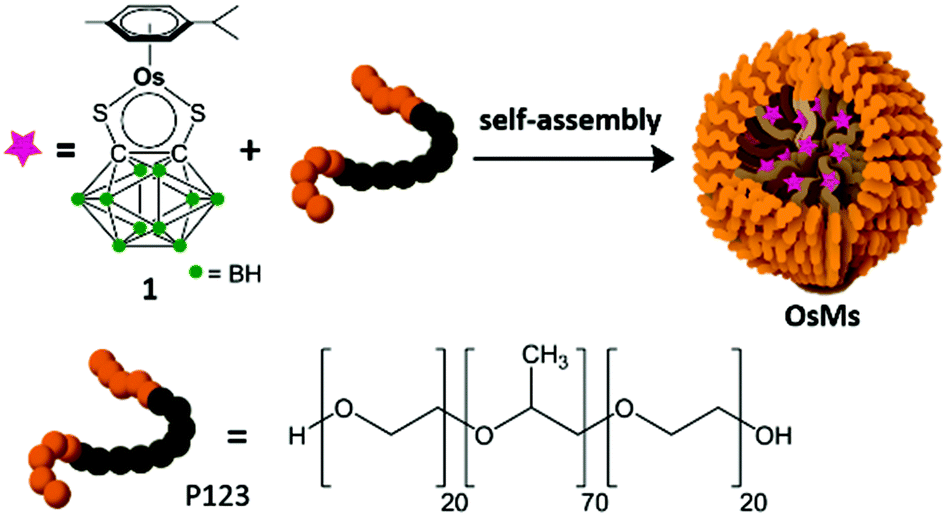 | ||
| Fig. 1 Self-assembly of block copolymer OsMs micelles containing encapsulated osmium carborane complex 1. | ||
However, this method produces only a small amount of nanocrystals owing to the high focus of the electron beam in an aberration-corrected HRTEM (ca. 200 × 200 nm2) and such a small scale production renders the investigation of the nanocrystal properties difficult. Focused high-energy electron irradiation also leads to a rapid destruction of the turbostratic graphitic structure. Here we report an important advance that now allows the fabrication of a large amount of osmium MNPs of controlled sizes (typically, between 1.5 nm and 50 nm) and without destruction of the graphitic support structure, through irradiation by a widely spread electron beam of a TEM to illuminate the entire TEM grid (3 × 3 mm2, Fig. S1†). The size of the osmium NPs can be varied by modulating the irradiation time, offering a facile method for controlling their diameters and potential properties. We characterise the MNPs by a combination of TEM, HRTEM, and AFM on the same grid. The ability to produce an abundance of large metal nanocrystals on doped graphitic structure also allowed determination of the osmium oxidation state by XPS after air exposure.
We deposited aqueous droplets of OsMs micelles (1 mg mL−1) onto a lacey carbon-coated TEM grid and, after drying, irradiated the whole grid with the electron beam of a TEM operating at 200 keV, for 12 h. As per irradiation with the highly focused beam of an aberration-corrected HRTEM on a small portion of the TEM grid (ca. 200 × 200 nm2) for 1 h,14 we observed the formation of a graphitic structure covered by dark areas of diameter 1.5 ± 0.9 nm (average for 500 spots) over much of the surface of the grid (Fig. 2a). To confirm the nature of the spots, we examined the same grid by HR-TEM and imaged it at high magnification within a short time (<4 min) to avoid effects due to highly focused beam irradiation. Fig. 2b–e show the images recorded on a specific area of the grid (originally one of the smaller holes of the lacey carbon film, now covered by the graphitic structure) at different magnifications. The elemental composition of the area was determined by energy-dispersive X-ray (EDX) analysis, which clearly identified the presence of Os (Fig. 2f).
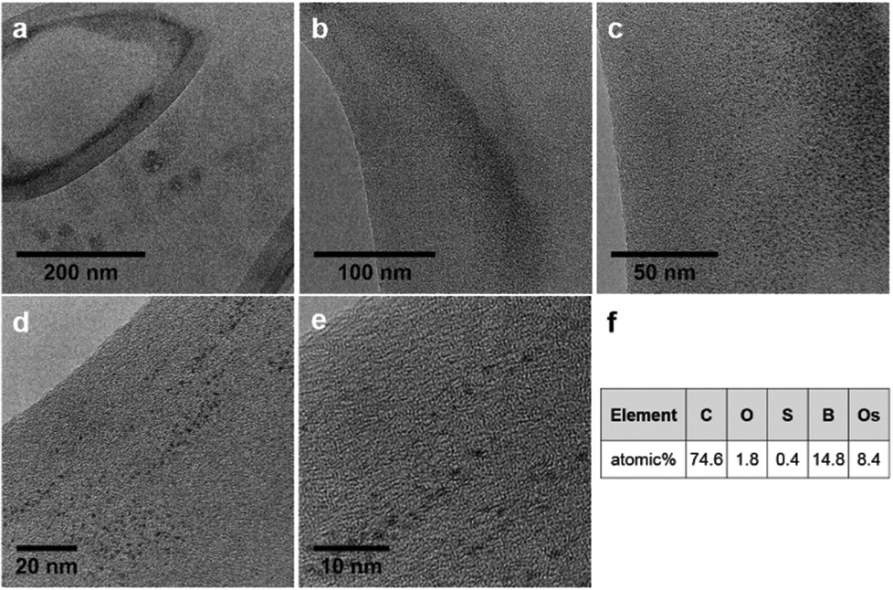 | ||
| Fig. 2 HRTEM imaging of a large number of nanocrystals produced by electron beam irradiation for 12 h, without destruction of the self-supporting matrix. (a–e) Imaging of the Os nanocrystals at different magnifications. (f) EDX analysis of boron K-, osmium O-, and sulfur L-edges in the area shown in (e). | ||
The graphitic structure was not destroyed during the MNP synthesis even after 12 h of irradiation and this was also true when the same grid was irradiated for another 16 h (total irradiation time 28 h). Remarkably, the growth of the nanocrystals continued during the further irradiation and the grid was found to be covered with larger (ca. 50 ± 6 nm diameter) Os nanoparticles (Fig. 3a and b). It is also apparent that these latter nanoparticles have sub-domains of smaller particles, suggesting that the growth of the bigger nanoparticles arises from coalescence of the smaller ones over time. Table 1 summarises these results.
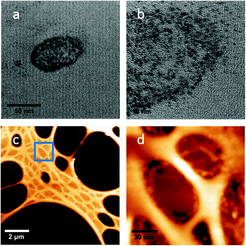 | ||
| Fig. 3 HRTEM and AFM images of large Os nanoparticles produced by widely spread electron beam irradiation for 28 h. (a) HRTEM image of a typical Os MNP. (b) Enlargement of the particle shown in (a). (c) Tapping mode AFM image showing the large and small holes in the lacey carbon structure; the latter are covered by the turbostratic graphitic structure. (d) Tapping mode AFM image showing the enlargement of the blue square area highlighted in (c), with Os MNPs appearing as small brighter bumps. | ||
| High-energy focused electron-beam irradiation14 | Widely spread electron-beam irradiation | ||
|---|---|---|---|
| Area irradiated | ca. 200 × 200 nm2 | All grid (3 × 3 mm2) | |
| Irradiation time (h) | 1 | 12 | 28 |
| Size of the MNPs (nm) | 1.8 ± 0.5 | 1.5 ± 1 | 50 ± 6 |
| Destruction of the graphitic structure | Yes | No | No |
To gain more information on the morphology of the nanoparticles, we studied the same grid (after 28 h of irradiation) by AFM (Fig. 3c and d). The images clearly show the large apertures in the lacey carbon structure (large black areas in Fig. 3c) and smaller shallow depressions with a depth of about 20–25 nm that correspond to the smaller holes in the lacey carbon, covered by the turbostratic graphitic structure (e.g. in the blue square in Fig. 3c, and magnified in Fig. 3d). These shallow depressions are not seen in a pristine TEM grid (Fig. S2†). Osmium MNPs appear as small bumps that are particularly visible within and on the edges of the shallow depressions (Fig. 3d). The diameter of the nanoparticles determined by AFM is consistent with the diameters determined by TEM. The osmium nanoparticles observed are relatively flat (height: 6 ± 3 nm), rather than spherical.
Notably, the structures of the Os nanoparticles appear to be air-stable when studied by electron microscopy: the TEM images are essentially the same before and after air-exposure. Furthermore, as found previously, under the vacuum conditions of TEM, the Os–Os distances in the MNPs are compatible with the presence of Os(0).14 However, metallic Os is known to be sensitive to air oxidation to form (volatile) OsO4. It might be expected that the MNPs would be even more sensitive. To gain more information on their reactivity, we performed XPS analysis of the particles after air exposure. Such measurements have been shown to be powerful to determine the oxidation state of osmium nano-islands, via the observation of identifiable Os signatures of different oxidation states in XPS spectra.18 We first examined five reference samples with known osmium oxidation states. These exhibited chemical shifts in their Os 4f spectra to higher binding energies with increasing oxidation state from 0 to +6 (Fig. 4a and b). Then, we acquired the XPS spectrum of the nanoparticles deposited on a TEM grid (Fig. 4c). Quantitative analysis of the data revealed two different bonding environments, with Os 4f7/2 components at 51.90 eV and 53.60 eV. These energies correspond most closely to the Os2+ and Os4+ reference samples, respectively, with the Os2+ accounting for the majority of the measured intensity.
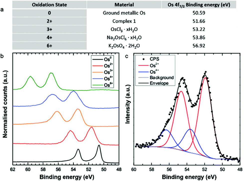 | ||
| Fig. 4 XPS analysis of the Os MNPs on a TEM grid after air exposure. (a) The five Os reference samples examined in this study and (b) corresponding Os 4f region. The position of the 4f7/2 components (peak at lower binding energy) are reported in the table in (a). (c) Os 4f region acquired from Os MNPs, revealing two different bonding environments, corresponding to Os2+ and Os4+, respectively (CPS, counts per second). | ||
The apparent absence of an Os(0) signature in the XPS spectrum of the MNPs clearly suggests that oxidation of the osmium atoms has occurred, perhaps favoured by the relatively flat rather than spherical shape of the particles. While this could in principle also be caused by the surface sensitivity of the technique, osmium atoms within the full height of the MNPs as determined by AFM should be detectable by XPS. The somewhat surprising predominance of Os2+ components might indicate that only a small amount of carborane-containing Os2+ complex 1 is decomposed under electron irradiation, even after 28 h of bombardment. We hypothesise that the kinetic energy of the e-beam is the main driving force for the MNP formation observed in TEM. However the fundamental mechanisms of interaction between incident electrons and the metallated particles are not understood, and will need to be explored in the future. Such understanding might reveal an enormous amount of valuable chemical information at the atomic scale.19–21 The Os4+ binding energy corresponds well with that reported in the literature for OsO2,22 but future work will also be needed to characterise quantitatively the chemical composition of the MNPs.
Conclusions
In addition to being a powerful analytical and imaging tool, the high-energy electron beam of HR transmission electron microscopes can also be utilised to modify in situ the structure and composition of various nano-scale materials, e.g. by phase transformation of primary nanoparticles, or reductive decomposition of inorganic/organometallic precursors, and to tailor the assembly and structure of metal nanoparticles.23–29 We have taken advantage of this high-energy electron source for producing very small nanocrystals of osmium via reduction of Os(II) precursors under the electron beam irradiation.14 Here we have introduced an important advance in this method by using a widely spread electron beam for producing large amounts of nm-sized Os nanocrystals. Furthermore, this new methodology induces less damage in the sample than a HRTEM beam – in particular no destruction of the supporting graphitic surface was observed – allowing the irradiation to be carried out over a much longer time (28 h versus 1 h). This method is expected to be easily generalised to provide a variety of other nano-metals and nano-alloys. Under the vacuum conditions of TEM, the Os–Os distances in the osmium nanoparticles are compatible with the presence of Os(0),14 but here we detected by XPS the presence of oxidised Os2+ and Os4+ ions after exposure of the nanocrystals to air. This study raises chemical questions about the composition of such MNPs synthesised in a TEM chamber, their reactivity towards growth and oxidation, and the chemistry which takes place at the atomic level. Highly sensitive new analytical techniques and methods are required that might allow such investigations and provide pathways to novel nanomaterials which exploit for their potential for unique magnetic and optical properties and chemical functionalisation.Acknowledgements
We thank the Leverhulme Trust (Early Career Fellowship No. ECF-2013-414 to NPEB), the University of Warwick (Grant No. RD14102 to NPEB), the ERC (Grant No. 247450 to PJS), and the EPSRC (EP/F034210/1 to PJS). L.M.A.P., J.L., and G.C. acknowledge financial support from the EU through the ERC Consolidator Grant “VISUAL-MS”.Notes and references
- D.-W. Lim, J. W. Yoon, K. Y. Ryu and M. P. Suh, Angew. Chem., Int. Ed., 2012, 51, 9814–9817 CrossRef CAS PubMed.
- J.-S. Lee, M. V. Kovalenko, J. Huang, D. S. Chung and D. V. Talapin, Nat. Nanotechnol., 2011, 6, 348–352 CrossRef CAS PubMed.
- Y. T. Zhu and X. Liao, Nat. Mater., 2004, 3, 351–352 CrossRef CAS PubMed.
- P. Wu and X.-P. Yan, Chem. Soc. Rev., 2013, 42, 5489–5521 RSC.
- M. Cargnello, V. V. T. Doan-Nguyen, T. R. Gordon, R. E. Diaz, E. A. Stach, R. J. Gorte, P. Fornasiero and C. B. Murray, Science, 2013, 341, 771–773 CrossRef CAS PubMed.
- Y. Yamada, C.-K. Tsung, W. Huang, Z. Huo, S. E. Habas, T. Soejima, C. E. Aliaga, G. A. Somorjai and P. Yang, Nat. Chem., 2011, 3, 372–376 CrossRef CAS PubMed.
- J. Jortner and C. N. R. Rao, Pure Appl. Chem., 2002, 74, 1491–1506 CrossRef CAS.
- C. Suryanarayana and B. Prabhu, in Nanostructured Materials (Second Edition), ed. C. C. Koch, William Andrew Publishing, Norwich, NY, 2007, pp. 47–90 Search PubMed.
- E. Giorgetti, F. Giammanco, P. Marsili and A. Giusti, J. Phys. Chem. C, 2010, 115, 5011–5020 Search PubMed.
- F. Wang, Z. Xie, H. Zhang, C.-y. Liu and Y.-g. Zhang, Adv. Funct. Mater., 2011, 21, 1027–1031 CrossRef CAS PubMed.
- X. Xia, L. Figueroa-Cosme, J. Tao, H.-C. Peng, G. Niu, Y. Zhu and Y. Xia, J. Am. Chem. Soc., 2014, 136, 10878–10881 CrossRef CAS PubMed.
- M. Cargnello, T. R. Gordon and C. B. Murray, Chem. Rev., 2014, 114, 9319–9345 CrossRef CAS PubMed.
- K. C. Poon, D. C. L. Tan, T. D. T. Vo, B. Khezri, H. Su, R. D. Webster and H. Sato, J. Am. Chem. Soc., 2014, 136, 5217–5220 CrossRef CAS PubMed.
- N. P. E. Barry, A. Pitto-Barry, A. M. Sanchez, A. P. Dove, R. J. Procter, J. J. Soldevila-Barreda, N. Kirby, I. Hands-Portman, C. J. Smith, R. K. O'Reilly, R. Beanland and P. J. Sadler, Nat. Commun., 2014, 5, 3851 CAS.
- N. P. E. Barry, A. Pitto-Barry, J. Tran, S. E. F. Spencer, A. M. Johansen, A. M. Sanchez, A. P. Dove, R. K. O'Reilly, R. J. Deeth, R. Beanland and P. J. Sadler, Chem. Mater., 2015, 27, 5100–5105 CrossRef CAS.
- A. Pitto-Barry and N. P. E. Barry, Polym. Chem., 2014, 5, 3291–3297 RSC.
- É. Kiss, T. Keszthelyi, G. Kormány and O. Hakkel, Macromolecules, 2006, 39, 9375–9384 CrossRef.
- C. K. Rhee, M. Wakisaka, Y. V. Tolmachev, C. M. Johnston, R. Haasch, K. Attenkofer, G. Q. Lu, H. You and A. Wieckowski, J. Electroanal. Chem., 2003, 554–555, 367–378 CrossRef CAS.
- T. W. Chamberlain, J. Biskupek, S. T. Skowron, P. A. Bayliss, E. Bichoutskaia, U. Kaiser and A. N. Khlobystov, Small, 2015, 11, 622–629 CrossRef CAS PubMed.
- T. Zoberbier, T. W. Chamberlain, J. Biskupek, N. Kuganathan, S. Eyhusen, E. Bichoutskaia, U. Kaiser and A. N. Khlobystov, J. Am. Chem. Soc., 2012, 134, 3073–3079 CrossRef CAS PubMed.
- T. W. Chamberlain, T. Zoberbier, J. Biskupek, A. Botos, U. Kaiser and A. N. Khlobystov, Chem. Sci., 2012, 3, 1919–1924 RSC.
- A. R. Siedle, R. A. Newmark, G. A. Korba, L. H. Pignolet and P. D. Boyle, Inorg. Chem., 1988, 27, 1593–1598 CrossRef CAS.
- X. Qi, Y. Huang, M. Klapper, F. Boey, W. Huang, S. D. Feyter, K. Müllen and H. Zhang, J. Phys. Chem. C, 2010, 114, 13465–13470 CAS.
- J.-U. Kim, S.-H. Cha, K. Shin, J. Y. Jho and J.-C. Lee, J. Am. Chem. Soc., 2005, 127, 9962–9963 CrossRef CAS PubMed.
- A. H. Latham and M. E. Williams, Langmuir, 2008, 24, 14195–14202 CrossRef CAS.
- A. H. Latham, M. J. Wilson, P. Schiffer and M. E. Williams, J. Am. Chem. Soc., 2006, 128, 12632–12633 CrossRef CAS PubMed.
- C. W. Huang, C. L. Hsin, C. W. Wang, F. H. Chu, C. Y. Kao, J. Y. Chen, Y. T. Huang, K. C. Lu, W. W. Wu and L. Chen, J. Nanoscale, 2012, 4, 4702–4706 RSC.
- J. W. Liu, J. E. Xu, Y. Ni, F. J. Fan, C. L. Zhang and S. H. Yu, ACS Nano, 2012, 6, 4500–4507 CrossRef CAS PubMed.
- Z. W. Wang and R. E. Palmer, Phys. Rev. Lett., 2012, 108, 245502 CrossRef CAS.
Footnote |
| † Electronic supplementary information (ESI) available. See DOI: 10.1039/c5dt03205a |
| This journal is © The Royal Society of Chemistry 2015 |