
 Open Access Article
 This Open Access Article is licensed under a Creative Commons Attribution-Non Commercial 3.0 Unported Licence
Non-volatile resistive memory devices based on solution-processed ultrathin two-dimensional nanomaterials
Chaoliang
Tan
a,
Zhengdong
Liu
ab,
Wei
Huang
bc and
Hua
Zhang
*a
aSchool of Materials Science and Engineering, Nanyang Technological University, 50 Nanyang Avenue, Singapore 639798, Singapore. E-mail: hzhang@ntu.edu.sg; Web: http://www.ntu.edu.sg/home/hzhang/
bKey Laboratory for Organic Electronics and Information Displays & Institute of Advanced Materials (IAM), Jiangsu National Synergetic Innovation Center for Advanced Materials (SICAM), Nanjing University of Posts & Telecommunications (NUPT), 9 Wenyuan Road, Nanjing 210023, China
cKey Laboratory of Flexible Electronics (KLOFE) & Institute of Advanced Materials (IAM), Jiangsu National Synergetic Innovation Center for Advanced Materials (SICAM), Nanjing Tech University (NanjingTech), 30 South Puzhu Road, Nanjing 211816, China
First published on 16th April 2015
Abstract
Ultrathin two-dimensional (2D) nanomaterials, such as graphene and MoS2, hold great promise for electronics and optoelectronics due to their distinctive physical and electronic properties. Recent progress in high-yield, massive production of ultrathin 2D nanomaterials via various solution-based methods allows them to be easily integrated into electronic devices via solution processing techniques. Non-volatile resistive memory devices based on ultrathin 2D nanomaterials have been emerging as promising alternatives for the next-generation data storage devices due to their high flexibility, three-dimensional-stacking capability, simple structure, transparency, easy fabrication and low cost. In this tutorial review, we will summarize the recent progress in the utilization of solution-processed ultrathin 2D nanomaterials for fabrication of non-volatile resistive memory devices. Moreover, we demonstrate how to achieve excellent device performance by engineering the active layers, electrodes and/or device structure of resistive memory devices. On the basis of current status, the discussion is concluded with some personal insights into the challenges and opportunities in future research directions.
 Chaoliang Tan | Chaoliang Tan received his BE degree in Applied Chemistry from the Hunan University of Science and Technology in 2009. After he got his ME degree in Applied Chemistry from South China Normal University in 2012, he moved to the School of Materials Science and Engineering of Nanyang Technological University in Singapore where he is currently pursuing his PhD degree under the supervision of Professor Hua Zhang. His research interests focus on the synthesis, assembly, and applications of two-dimensional nanosheets (e.g., graphene and transition metal dichalcogenides) and their composites. |
 Zhengdong Liu | Zhengdong Liu obtained his BS degree from Hengyang Normal University in 2010. He then moved to the Nanjing University of Post & Telecommunications for his graduate studies under the supervision of Prof. Wei Huang. From April 2012 to January 2015, he was a visiting student in Prof. Hua Zhang's group at Nanyang Technological University in Singapore. His current PhD thesis focuses on the design and synthesis of novel semiconducting polymers for flexible organic electronic devices, including memory devices and light emitting devices. |
 Wei Huang | Wei Huang received his PhD from Peking University in 1992. In 1993, he started his postdoctoral research in the National University of Singapore. In 2001, he was appointed as a chair professor in Fudan University, where he founded and chaired the Institute of Advanced Materials (IAM). In 2006, he was appointed the Vice President of Nanjing University of Posts and Telecommunications. Now, he is the President of NanjingTech University. He was elected as Academician of Chinese Academy of Sciences in 2011. His research interests include organic/plastic materials and devices, nanomaterials and nanotechnology, etc. |
 Hua Zhang | Hua Zhang obtained his BS and MS degrees from Nanjing University in 1992 and 1995, respectively, and completed his PhD with Prof. Zhongfan Liu at Peking University in 1998. As a Postdoctoral Fellow, he joined Prof. Frans C. De Schryver's group at Katholieke Universiteit Leuven (Belgium) in 1999, and then moved to Prof. Chad A. Mirkin's group at Northwestern University in 2001. After working at NanoInk Inc. (USA) and the Institute of Bioengineering and Nanotechnology (Singapore), he joined Nanyang Technological University in July 2006. His current research interests focus on the synthesis of two-dimensional nanomaterials and carbon materials (graphene and carbon nanotubes), and their applications in nano- and bio-sensors, clean energy, water remediation, etc. |
Key learning points(1) The unique advantages of solution-processed ultrathin 2D nanomaterials for non-volatile memory devices.(2) Summary of the general techniques for fabrication of non-volatile memory devices based on solution-processed ultrathin 2D nanomaterials. (3) The construction of all-carbon resistive memory devices based on graphene nanosheets. (4) Summary of the effect of chemically modified/functionalized 2D nanomaterials with other materials, such as polymers and inorganic nanoparticles, on the memory performance. (5) Demonstration of the device performance improved by rational design of device structures and active materials. |
1. Introduction
The rapidly growing demand for non-volatile memory cells in modern electronics has driven the extensive exploration of new-generation data storage devices since the traditional Si-based information storage technology faces theoretical and physical limits. In general, from the structure point of view, there are three types of electronic memory devices, i.e. transistor-type, capacitor-type and resistor-type devices.1 In contrast to the transistor- and capacitor-type ones, the simple structure of resistor-type memory devices consisting of an active layer sandwiched between two electrodes makes it possible to fabricate a three-dimensional (3D)-stacking structure and thus to achieve high density data storage.1 In two-terminal resistive memory devices, the data storage and access are defined by the electrical bistability, i.e. the low resistance state (ON state) and the high resistance state (OFF state), which correspond to the sequences of “1” and “0” in the modern computers.1 During the development of modern electronics, only the non-volatile resistive memory devices with excellent characters, such as a high ON/OFF current ratio (e.g. >106), excellent cycling stability (e.g. >106 cycles), long retention time (e.g. >10 years), ultra-low switching voltage (e.g. near zero) and low cost, could be considered for practical applications.2 Due to their structural simplicity, the design and synthesis of active materials for resistive memory devices is the key topic for the construction of high-performance resistive memory devices. Previous studies have demonstrated that low-dimensional inorganic–polymer hybrid nanomaterials, including metal nanoparticles (NPs), semiconductor quantum dots (QDs), fullerenes or carbon nanotubes (CNTs) hybridized with polymers, could be attractive active materials for fabrication of next-generation non-volatile resistive memory devices.3 However, until now, they still cannot meet the criteria for the real data storage technology in modern electronics.2 Therefore, exploration of novel electronically active nanomaterials or composites as active layers for high-performance non-volatile resistive memory devices is urgently required.Ultrathin two-dimensional (2D) nanomaterials, such as graphene and transition metal dichalcogenide (TMD) nanosheets, including MoS2, WS2, TiS2, TaS2, etc., have attracted increasing attention in the past few years, due to their 2D morphology and ultrathin thickness.4–9 As a family of newly emerging nanomaterials, they have shown many unique characteristics that are unattainable with the other forms of counterparts, such as a large specific surface area, excellent mechanical stiffness and flexibility, and high transparency.4–10 The appealing physical, chemical and electronic features of these 2D nanomaterials make them very promising in a variety of potential applications, such as optoelectronic/electronic devices,4,6,7 catalysis,5–7 sensors,5–7 energy storage and conversion6–9 and biomedicine.10 The prospect of their potential applications in turn leads to great research efforts in developing various kinds of effective synthetic methods for ultrathin 2D nanomaterials. Recent success in the preparation of solution-processed ultrathin 2D nanomaterials in high yield and on a large scale through various methods has trigged great interest in their utilization as building blocks for fabrication of electronic devices, especially the advanced information storage devices. There are several unique advantages of ultrathin 2D nanomaterials for construction of non-volatile resistive memory devices compared to metal NPs, semiconductor QDs, fullerenes and CNTs: (1) the electronic state of some ultrathin 2D nanomaterials, e.g. graphene oxides (GO) and reduced GO (rGO), is easily tuned by controlling the amount of functional groups on their surface. (2) The large lateral size and ultrathin thickness of 2D nanomaterials allow for the fabrication of high quality thin films via simple techniques, such as vacuum filtration, spin-coating, spray-coating and ink-jet printing. (3) The high transparency and excellent flexibility of ultrathin 2D nanomaterials make them promising for fabrication of transparent, flexible and wearable electronic resistive memory devices.
In this tutorial review, we aim to introduce the recent progress in the utilization of solution-processed ultrathin 2D nanomaterials, especially graphene and MoS2, for non-volatile resistive memory devices. First, non-volatile resistive memory devices based on GO/rGO sheets and their composites will be introduced, such as GO/rGO and GO/rGO functionalized with other materials (e.g. polymers and inorganic NPs) as the active layers, highly conductive rGO films as the electrodes, and fabrication of all-carbon resistive memory devices based on GO/rGO sheets. Then, we will discuss non-volatile resistive memory devices by using solution-processed MoS2 nanosheet-based composites as the active layers. Meanwhile, we will also demonstrate how to achieve excellent device performance by engineering the active layer materials and/or electrodes. Finally, we will give some personal insights into the current challenges and future opportunities in this promising field.
2. Non-volatile resistive memory devices based on graphene and its derivatives
The most studied solution-processed graphene-related nanosheets are GO and rGO. Note that GO is electrically insulating, while the rGO sheets obtained from the reduction of GO by various kinds of methods could be highly conductive after the removal of oxygen-containing groups from their surface.5 The oxidation state of graphene sheet can be changed by fine-tuning the amount of the oxygen-containing functional groups on its surface. The solution processability and unique electronic property of GO/rGO allow them to be easily fabricated as a thin film for device application via various solution-based techniques.11 Due to the excellent flexibility, transparency, easy film formation and tunable electronic property, GO/rGO sheets have shown great promise in the fabrication of non-volatile resistive memory devices.11 Notably, graphene-related nanosheets could play different roles in memory devices. For example, GO and partially reduced rGO sheets can be directly used as the active layer in memory cells. GO and rGO sheets can be further functionalized with other materials, such as polymers or inorganic NPs, and then used as the active layer in memory devices. The highly conductive rGO films can also be used as flexible, transparent and low-cost electrodes in memory devices. Importantly, all-carbon non-volatile memory devices have been successfully constructed by using the highly conductive rGO films as both the top and bottom electrodes and partially reduced rGO as the active layer. In this section, we will focus on the discussion of resistive memory devices based on the solution-processed GO and rGO sheets. Table 1 summarizes the non-volatile resistive memory devices with GO, rGO or their composites as active layers.| Active layer materials | Electrodes | Technique for fabrication of active layer | Memory effect | Switching voltage | ON/OFF current ratio | Stable retention time | Ref. |
|---|---|---|---|---|---|---|---|
| GO |
Top: Cu
Bottom: Pt |
Vacuum filtration | Rewritable | <1 V | ∼20 | 104 s | 12 |
| GO |
Top: Al
Bottom: Al |
Spin-coating | Rewritable | ∼2.5 V | ∼102 | 105 s | 13 |
| GO |
Top: Al
Bottom: ITO |
Spin-coating | WORM | ∼2 V | ∼103 | — | 14 |
| GO |
Top: LiF/Al
Bottom: ITO |
Spin-coating | WORM | ∼3 V | ∼5.7 × 10⁴ | — | 15 |
| rGO |
Top: Al
Bottom: ITO |
Spin-coating | WORM | ∼5 V | ∼103 | 105 s | 16 |
| N-rGO |
Top: Au or Al
Bottom: ITO |
Spin-coating | Rewritable | 1–3 V | ∼102 | 103 s | 17 |
| GO–PVK |
Top: Al
Bottom: ITO |
Spin-coating | Rewritable | ∼−2 V | ∼103 | 3 h | 20 |
| TPAPAM–GO |
Top: Al
Bottom: ITO |
Spin-coating | Rewritable | ∼−1 V | ∼103 | 3 h | 21 |
| PFCF–rGO |
Top: Al
Bottom: ITO |
Spin-coating | Rewritable | ∼−1.2 V | ∼104 | 3 h | 22 |
| GO–PI |
Top: Ag
Bottom: ITO |
Spin-coating | Rewritable | ∼3.5 V | ∼105 | 1.4 × 10³ s | 23 |
| GO–PFCz |
Top: Al
Bottom: ITO |
Spin-coating | Rewritable | ∼−1.3 V | ∼103 | 3 h | 24 |
| rGO–ferrocene |
Top: Al
Bottom: ITO |
Spin-coating | Rewritable | ∼2.1 V | ∼103 | 103 s | 25 |
| PANI–GO |
Top: Al
Bottom: ITO |
Spin-coating | Rewritable | ∼−1.3 V | ∼104 | 3 h | 26 |
| PS-b-P4VP–GO |
Top: Al
Bottom: ITO |
Spin-coating | WORM | ∼−6.7 V | ∼105 | 104 s | 27 |
| rGO–PVK |
Top: Al
Bottom: ITO |
Spin-coating | rGO = 2 wt%: WORM | ∼−2.1 V | ∼8 × 10³ | >104 s | 28 |
| rGO = 4 wt%: rewritable | ∼−1.7 V | 103 | >104 s | ||||
| AuNP–frGO |
Top: Al
Bottom: ITO |
Spin-coating | Rewritable | ∼−2 V | 103 | >700 s | 29 |
2.1. Graphene oxide (GO) and partially reduced graphene oxide (rGO) sheets as the active layers
The unique structure of GO and partially reduced rGO enables them to be used as promising active materials in resistive memory devices.12–17 As a typical example, Li and coworkers demonstrated the fabrication of a non-volatile resistive memory device based on GO sheets.12 The GO film was prepared via a simple vacuum filtration method, in which the thickness of GO film can be controlled by varying the concentration of GO solution and the filtration time. The GO film was then integrated into a memory diode sandwiched between Pt and Cu electrodes. The resultant device exhibited a typical rewritable memory effect with low switching voltage (∼0.8 V) and long retention time (>104 s). However, the ON/OFF current ratio is very low (∼20). The charge trapping and detrapping on the oxygen-containing groups of GO sheets as well as the diffusion of the top Cu electrode might be responsible for the switching effect. Later on, Choi and coworkers reported the fabrication of a flexible resistive memory device by using GO film as the active layer (Fig. 1).13 A simple spin-casting process was used to fabricate large-area uniform GO film from GO suspension. The prepared GO film could be transferred to any substrates for integration of electronic devices. In this flexible device, Al electrode lines were used as both the bottom and top electrodes and polyethersulfone (PES) foil was used as the flexible substrate (Fig. 1a). The resultant device exhibited a typical bipolar rewritable memory effect with an ON/OFF current ratio of ∼100 (Fig. 1b), which is 5 times as much as that of the aforementioned GO-based device (∼20).12 No noticeable degradation was detected on the device performance even after continuous bending of 1000 times (Fig. 1c and d), indicating the excellent feasibility of the flexible device. A long retention time (>105 s) and a switching voltage of ∼2.5 V were obtained in this device (Fig. 1e). The ON/OFF states of the device did not show obvious change even after 100 sweep cycles, indicating its good reproducibility (Fig. 1f). It was believed that the switching behavior of the device is governed by a dual mechanism of oxygen migration and Al diffusion.14 In addition, the Al diffusion in the GO layer determines the long term reliability of the device.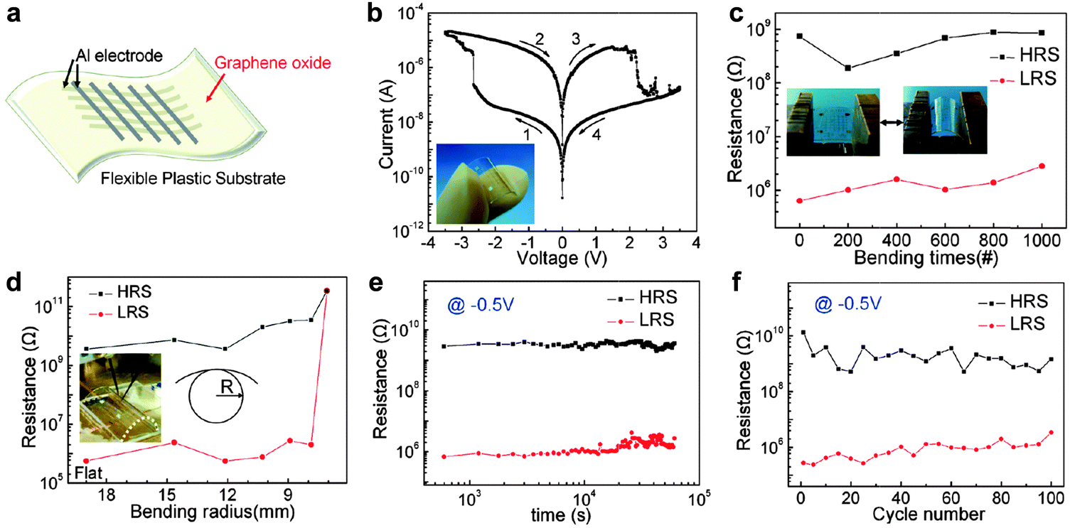 | ||
| Fig. 1 (a) Schematic illustration of GO-based flexible memory devices. (b) Typical I–V curve of an Al/GO/Al/PES device. The inset is the photograph of a device. (c) Continuous bending effect of an Al/GO/Al/PES device. The insets show photographs of a device in two bending states. (d) The resistance ratio between the high resistance state (HRS) and low resistance state (LRS) as function of the bending radius (R). The inset is the photograph of an I–V measurement performed under a flexed condition. (e) Retention test of Al/GO/Al/PES device read at −0.5 V. (f) Endurance performance of an Al/GO/Al/PES device measured during 100 sweep cycles. Reproduced with permission from ref. 13. Copyright 2010, American Chemical Society. | ||
Besides the flash memory effect, write-once-read-many-times (WORM) type switching behavior has also been realized by using GO as the active layer by Huang and coworkers.15 The GO film was prepared by a simple spin-coating technique on an indium tin oxide (ITO) substrate. The device with configuration of ITO/GO film/LiF/Al presented irreversible electrical transition of the OFF state to ON state during the voltage sweeping, indicating a typical WORM memory effect of the resistive diode, which might be attributed to the charge trapping in the GO layer. Note that its ON/OFF current ratio is as high as 5.7 × 10⁴.
In addition to GO, rGO sheets have also been used as active layers for construction of non-volatile resistive memory devices. The rGO sheets discussed in this section are partially reduced GO sheets. Recently, the integration of a memory diode based on rGO sheets was demonstrated (Fig. 2).16 The GO sheets were reduced via the ultraviolet irradiation catalyzed with 2,2,6,6-tetramethyl-4-piperidinol (TMP) (Fig. 2a). This green and efficient method could selectively remove the sp2-hybridized oxygen functional groups but reserve the epoxy and hydroxyl groups on the GO sheets. Although being partially reduced, the resultant rGO sheets still retained their good solubility in aqueous solution, making it easy the preparation of thin film via a solution processing technique. The rGO sheets were then integrated into a memory device with configuration of Au/rGO/ITO via a simple spin-coating technique (Fig. 2b). The thickness of rGO film in this device is about 30 nm. The fabricated device exhibited a typical WORM switching behavior with a high ON/OFF current ratio of 103 and a switching voltage of ∼5 V (Fig. 2c). Intriguingly, the rGO-based device presented an excellent stability and no significant degradation could be observed even after a retention time of as long as 105 s (Fig. 2d). It was found that this rGO-based diode is much more stable compared with the GO-based device with a same device configuration (Fig. 2e). It is believed that the enhanced stability of the rGO-based device is attributed to the less active and hydrophilic carboxyl and carbonyl groups on the rGO sheets. As another example, Lee and coworkers also reported the fabrication of a resistive memory device based on rGO sheets.17 The GO sheets were thermally reduced at a relatively high temperature (150 °C) in dimethylformamide (DMF). Surprisingly, it was found that pyridinium N was doped in the framework of rGO sheets during the thermal reduction process. The resultant N-doped rGO (N-rGO) sheets with ∼3% doped N atoms exhibited an optical energy band gap of 1.7–2.1 eV. The as-prepared N-rGO sheets were then used as the active layer to fabricate a memory device by using ITO and Al as the bottom and top electrode, respectively. The fabricated device exhibited a typical rewritable memory effect with a switching voltage of ∼3 V, which is different from our previously reported rGO-based WORM type memory device.16 The device did not show obvious degradation ever after 100 continuous sweeping cycles, indicating its excellent reproducibility. The ON/OFF current ratio for this device is about 102 with a retention time of more than 103 s. It was suggested that the oxygen content of N-rGO sheets and the interplay of functional groups between N-rGO sheets played essential roles in determining the switching behavior of the device.
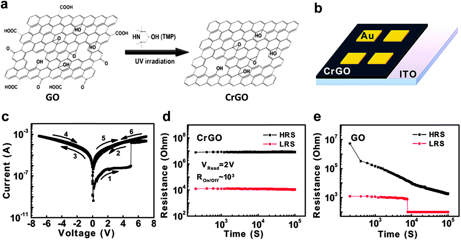 | ||
| Fig. 2 (a) Schematic illustration of the selective reduction of GO. (b) Schematic illustration of the Au/rGO/ITO memory device. (c) Typical I–V curve of the fabricated Au/rGO/ITO memory device. (d) Retention test of the fabricated Au/rGO/ITO memory device at the reading voltage of 2 V. (e) Retention test of the Au/GO/ITO memory device with a same configuration with the rGO-based device. Reproduced with permission from ref. 16. Copyright 2012, American Chemical Society. | ||
2.2. Graphene-based polymer composites as the active layers
In recent years, polymer-based resistive memory devices have been recognized as one of the promising alternatives to the conventional Si-based data storage technology owing to their advanced features of flexibility, solution processing and 3D-stacking capability.18 The electrical switching behaviors of polymer-based memory diodes can be rationally tuned by engineering the molecular structures of active polymers. Note that polymers with aromatic groups can be functionalized on GO/rGO sheets via the covalent bonding or strong π–π stacking interaction.19 Bearing this in mind, the modification of GO/rGO sheets with polymers as the active layer for memory devices could be a promising strategy for engineering the electrical switching behavior of GO/rGO-based resistive memory devices.As a typical example, Kang and coworkers used GO–polymer composites as the active layer in memory devices.20 The poly(N-vinylcarbazole) (PVK) macromolecule was covalently grafted on GO sheets via the amido bonding to form the PVK-functionalized GO composite (GO–PVK). Note that the resultant GO–PVK composite can be well dispersed in a number of organic solvents. Then, the GO–PVK film with a thickness of ∼100 nm was integrated in a memory device as the active layer by using ITO and Al as the bottom and top electrode, respectively. The fabricated GO–PVK-based memory cell exhibited bistable electrical switching behavior and a rewritable memory effect with a switching voltage of ∼−2 V, an ON/OFF current ratio of more than 103 and a stable retention time of more than 104 s. It is believed that the modified PVK molecules can form a thin coating layer on the GO surface, serving as a tunneling barrier for charge transport between neighboring GO sheets. In another work, the same group decorated a soluble triphenylamine-based polyazomethine (TPAPAM) polymer on GO sheets via amido bonding to form a TPAPAM–GO composite (Fig. 3a).21 By using this resultant composite as the active layer, the fabricated device with a configuration of ITO/TPAPAM–GO/Al also showed a typical rewritable memory effect (Fig. 3b). The switching voltage of this device is as low as −1 V, which is lower than that of the GO–PVK based device (∼−2 V).20 The ON/OFF current ratio and stable retention time are as good as those of the GO–PVK composite-based device (Fig. 3c). Later on, a number of polymers, such as poly-[{4,4′-(9H-fluorene-9,9-diyl)bis(N,N-diphenylbenzenamine)}{4-(9H-carbazol-9-yl)benzaldehyde}(9,9-dihexyl-9H-fluorene)] (PFCF-CHO), poly[{9,9-di(triphenylamine)fluorene}(9,9-dihexylfluorene)(4-aminophenylcarbazole)] (PFCz), polyimide (PI), ferrocene and polyaniline (PANI), were covalently functionalized on GO/rGO sheets,22–26 a series of novel GO/rGO-based polymer composites were prepared and then integrated into memory devices with similar rewritable memory effects.22–26 In addition to the rewritable memory effect, a WORM memory effect has been also achieved on GO–polymer based memory devices. For example, Chen and coworkers reported the preparation of a new composite via hydrogen bonding by simply mixing the block copolymer of poly(styrene-block-4-vinylpyridine) (PS-b-P4VP) with GO sheets.27 The resultant composite as the active layer for memory devices with Al and ITO as top and bottom electrodes, respectively, exhibited a typical WORM switching behavior with switching voltages in the range of −5.5 to −7.0 V. Stable retention of two states of the device was observed for at least 104 s without any degradation, indicating the good stability of the device. The ON/OFF current ratio of the device is as high as 105.
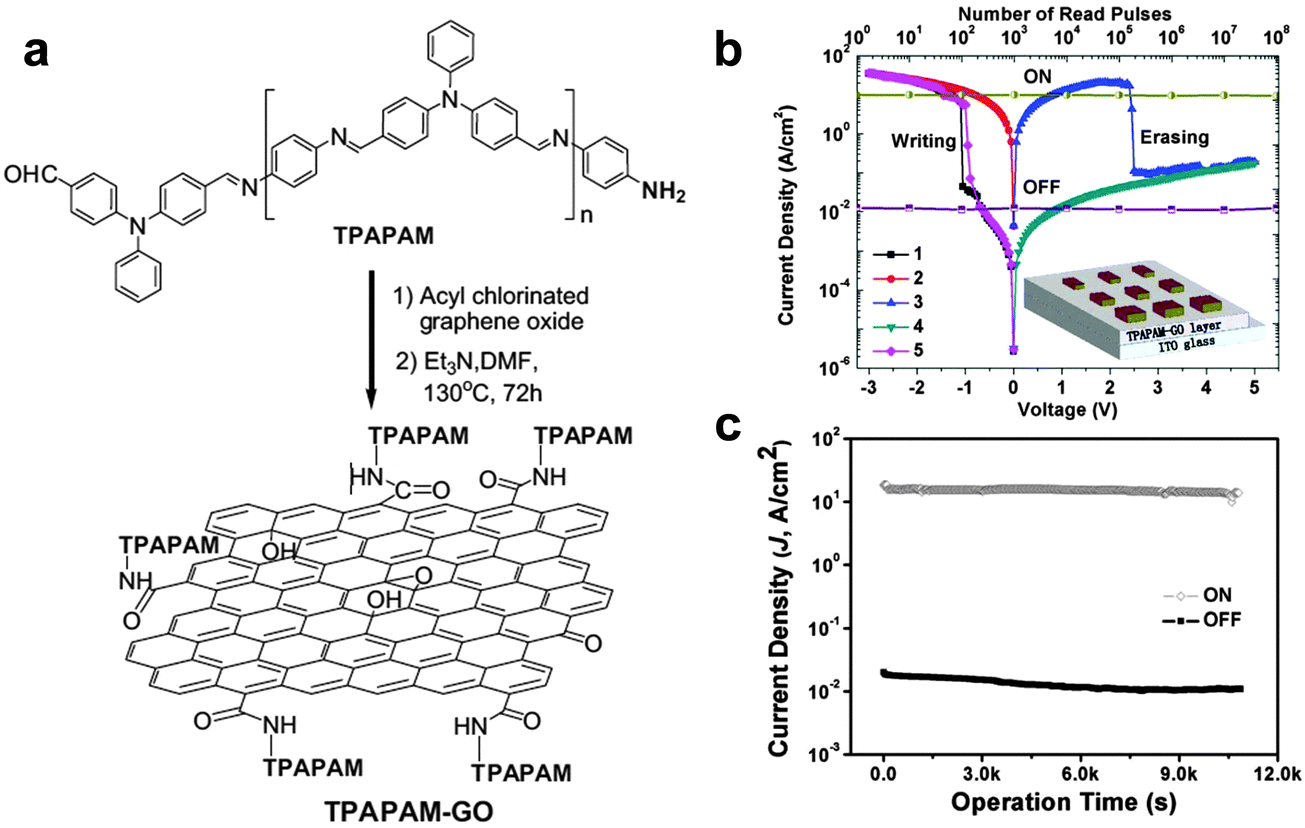 | ||
| Fig. 3 (a) Schematic illustration of synthesis of TPAPAM–GO. (b) I–V characteristics and stability tested in either ON or OFF state of the ITO/TPAPAM–GO/Al device. The inset shows the schematic diagram of single-layer memory devices. (c) Effect of the operation time (at −1 V) on the device current density in the OFF and ON states. Reproduced with permission from ref. 21. Copyright 2010, John Wiley & Sons, Inc. | ||
Interestingly, Shang and coworkers demonstrated that the electrical behaviors of memory devices based on the rGO–PVK composite can be fully tuned by varying the weight content of rGO in the PVK matrix.28 The rGO–PVK composite was prepared by simply mixing PVK with rGO sheets in solution and then integrated in memory devices as the active layer. It was found that the electrical conductance behavior of the device is highly dependent on the weight content of rGO in the rGO–PVK composite. Specifically, the device with 0.5 wt% of rGO exhibited low-conductance and no switching behavior was observed, which is similar to the pure PVK-based devices. When the weight content of rGO increased to 2 wt%, a WORM memory effect was achieved on the device with a switching voltage of ∼−2.1 V. The ON/OFF current ratio could reach 8 × 10³. Intriguingly, when the weight content of rGO increased to 4 wt%, the resultant device presented a rewritable switching behavior with an ON/OFF current ratio of more than 103. A single conductor state with good conductivity of the fabricated device was observed when the weight content of rGO further increased to 6 wt%. The tunable switching effect of devices based on the rGO–PVK composite is attributed to the content-dependent electron trapping in the rGO sheets embedded in the electron-donating–hole-transporting PVK matrix.
2.3. Graphene-based other composites as the active layers
In addition to polymers, GO/rGO sheets have also been hybridized with other materials, including Au NPs and cellulose, to form hybrid nanomaterials for integration of non-volatile resistive memory devices. For example, Lee and coworkers reported the fabrication of memory devices based on AuNP-functionalized rGO sheets, referred to as AuNP–frGO.29 Memory devices with both horizontal and vertical structures were successfully fabricated by using the same active material. For the horizontally structured device, single- and double-layer GO sheets were first spin-coated on patterned Au electrodes deposited on a Si/SiO2 substrate (Fig. 4a). The GO sheets were then reduced to rGO with hydrazine vapor. After that, 4-mercapto-benzenediazonium tetrafluoroborate molecules were assembled onto rGO to form a thiol-terminated surface (Fig. 4b). Finally, Au NPs were immobilized on the surface through strong Au–S bonding, referred to as AuNP–frGO (Fig. 4c). For the vertical device, the AuNP–frGO thin film with a thickness of ∼50 nm was prepared by spin-coating of the AuNP–frGO suspension onto an ITO electrode, followed with the vapor deposition of 200 nm thick Al as the top electrode (Fig. 4d). Both the horizontal and vertical devices showed reproducible and noticeable switching behaviors. It was found that the horizontal device exhibited a reversible hysteresis during the voltage sweep, which can be clarified as the volatile dynamic random access memory (DRAM) (Fig. 4e), while the vertical device presented a typical non-volatile rewritable memory effect (Fig. 4f). In another example, Valentini and coworkers reported the construction of a resistive memory device based on a GO–cellulose hybrid thin film.30 The device with a rewritable memory behavior was prepared by simply drop-casting aqueous solution of GO–cellulose inbetween electrodes.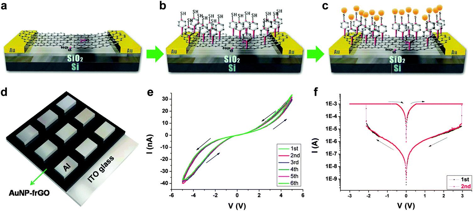 | ||
| Fig. 4 (a–d) Schematic illustration of fabrication process for the AuNP–frGO based memory devices. (e) I–V characteristics on linear scales of the horizontal AuNP–frGO based device. (f) I–V characteristics on log scales of the vertical AuNP–frGO based device. Reproduced with permission from ref. 29. Copyright 2011, American Chemical Society. | ||
2.4. Graphene as the electrode for non-volatile resistive memory devices
Generally, the most widely used electrodes in conventional memory devices are metals (e.g. Au, Pt, Al, Cu, etc.), ITO, and p- or n-doped Si. However, the rapid development in modern electronics is expected to use electrodes that are flexible, wearable, stretchable and transparent. In this case, the conventional electrode materials cannot meet these requirements. The excellent conductivity, flexibility, transparency, cost-effectiveness and environment friendliness of graphene make it a very promising electrode material for integration of electronic devices to satisfy the requirements of future electronics.31 Importantly, carbonaceous materials are sustainable in comparison with those conventional electrode materials. Although mechanically-exfoliated and chemical vapor deposition (CVD)-grown graphene sheets have been widely used as electrodes in electronics due to their outstanding conductivity, their practical application is limited by due to the low-yield production or extreme synthetic conditions (e.g. high temperature and high vacuum).32 In contrast, the solution-processed GO sheets, which can be produced in high yield and on a large scale in solution at low cost, allow us to easily fabricate electrodes. Specifically, highly conductive rGO sheets that can be obtained by reduction of GO sheets could be fascinating electrodes for integration of electronic devices.31Recently, the utilization of highly conductive rGO film as the electrode in memory devices was demonstrated by our group.33 A simple and effective method was developed to reduce GO sheets to get highly conductive rGO films by combination of low-temperature chemical reduction with a smeared hydrazine solution and a physical multilayer stacking approach. Briefly, GO film was first prepared from GO sheets by a simple vacuum filtration method. Note that the thickness of GO film could be easily tuned by changing the concentration and volume of the GO suspension. The dried GO film was immersed in a hydrazine solution and then heated at 100 °C for 18 h to remove the oxygen-containing groups. After the repetition of the aforementioned procedure several times, multilayer-stacked rGO film with low resistance (∼160–500 Ω sq−1) and high conductivity (26 S cm−1) was obtained and then further used as the bottom electrode in a polymer memory device. The resultant polymer device with configuration of rGO/poly(3-hexylthiophene) (P3HT):phenyl-C61-butyricacid methyl ester (PCBM)/Al gave a WORM memory effect with a switching voltage of ∼−1.4 V. Importantly, the ON/OFF current ratio of this device could reach up to 106. Later on, the effect of conductivity of the rGO electrode on the performance of the polymer memory device was systematically explored.34 It was demonstrated that the higher conductivity of the rGO electrode gave better device performance of the polymer memory device. The ON/OFF current ratio increased with the conductivity of the rGO electrode, and the switching voltage decreased with the increase of the conductivity of the rGO electrode. As another example, Lee and coworkers demonstrated the fabrication of non-volatile molecular memory devices by using an azobenzene monolayer as the active layer and rGO films as both the bottom and top electrodes.35 Briefly, after a GO film was deposited onto a substrate via a spin-coating process, it was reduced by hydrazine vapor to obtain rGO film, which was used as the bottom electrode. After that, a monolayer of azobenzene was assembled on the rGO film as the active layer. The top rGO electrode array was finally fabricated by spraying rGO solution. Finally, a device with a configuration of rGO/azobenzene monolayer/rGO was obtained. It is worth pointing out that this device was fabricated by an all-solution-processed approach. The fabricated device showed a typical rewritable memory effect with a retention time of more than 104 s. It is suggested that the rewritable memory effect of the device is attributed to the reversible trans–cis isomerization of the azobenzene monolayer under the applied voltage.
Recently, Wong and coworkers reported the reduction of GO sheets by a laser scribing technique as the bottom electrode for fabrication of memory devices (Fig. 5a).36 The GO film was first deposited on the polyethylene terephthalate (PET) substrate coated on a digital video disc (DVD) via a simple drop-casting method (Fig. 5b). The dried GO film was patterned through DVD laser-induced reduction in a LightScribe DVD drive. The resultant rGO pattern could be directly used as the electrode for integration of electronic devices. The unique features, such as low cost, time efficiency and transfer free, make this method very attractive for fabrication of rGO pattern. Then, HfOx thin film with thickness of 10 nm was deposited on the patterned rGO electrode as the active layer, and the curable silver paste was used as the top electrode at room temperature (Fig. 5b). It is worth pointing out that the laser-scribing technology is very time-efficient and the fabrication of patterned memory array with an area up to 100 cm2 could be finished within 25 min. Compared to lithography, photoresist is not required in this process. Therefore, the patterned rGO could remain clean, which is beneficial for further device fabrication. The fabricated resistive memory device with a configuration of Ag/HfOx/rGO exhibited a resistive rewritable memory effect (Fig. 5c–e). Note that the 100th I–V curve of the device is almost the same as the 1st cycle (Fig. 5c), indicating its excellent reproducibility. The excellent performance of the device proved that the laser-scribing technology is potentially applicable for the construction of more cost- and time-effective electronic devices based on rGO electrodes.
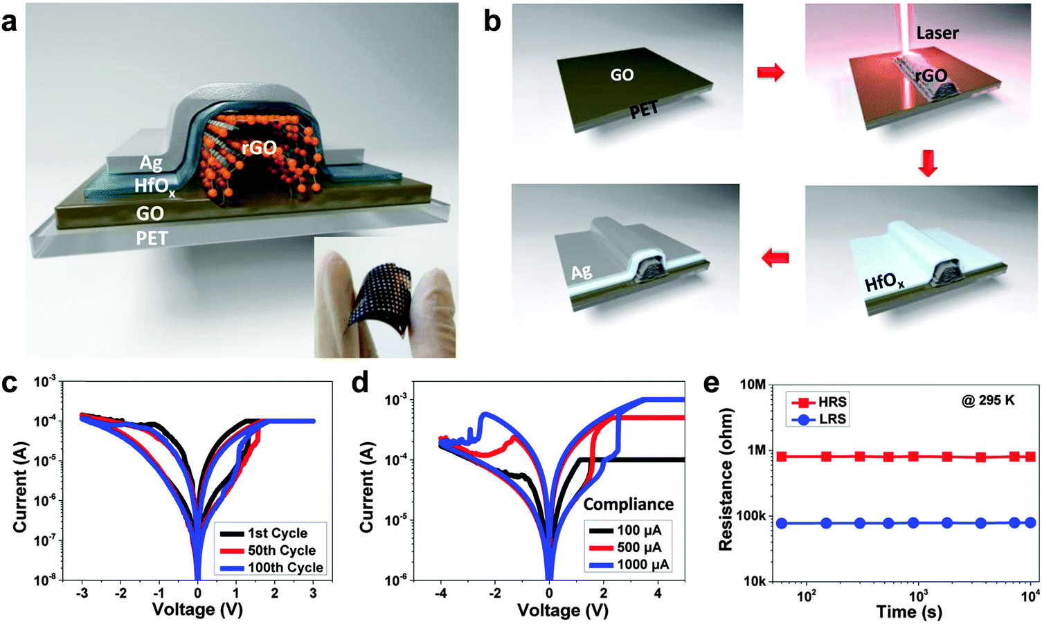 | ||
| Fig. 5 (a) Schematic illustration of the device with configuration of Ag/HfOx/rGO/PET. The inset shows the photo of fabricated devices. (b) Schematic illustration of the fabrication process of device. (c) Resistive switching behaviors of the device at the 1st, 50th and 100th cycle, respectively. (d) Resistive switching behavior of the device under different current compliance. (e) Retention measurement of the Ag/HfOx/rGO/PET device at room temperature. Reproduced with permission from ref. 36. Copyright 2014, American Chemical Society. | ||
2.5. All-carbon non-volatile resistive memory devices based on graphene
Due to their excellent electronic properties, flexibility, cost-effectiveness and environment friendliness, all-carbon electronic devices have been recognized as one of the most promising candidates for the future electronics and optoelectronics.37,38 It has been demonstrated that GO and partially reduced GO can be promising as active layers for fabrication of non-volatile resistive memory devices. Meanwhile, being highly conductive, rGO films reduced at high temperature have shown great potential as electrodes in polymer-based resistive memory devices. Inspiringly, our group first demonstrated the fabrication of full solution-processed, all-carbon, flexible non-volatile memory devices by using highly conductive rGO films as both bottom and top electrodes and partially reduced rGO sheets as the active layer.39 The key challenge for this device is to transfer the rGO top electrode and remove poly(methyl methacrylate) (PMMA) without influence on the quality of the active layer (Fig. 6a). Briefly, the GO films were patterned by a “scratching” method on the Si/SiO2 substrate, which were then annealed at high temperature (1000 °C) to obtain highly conductive rGO patterns. The patterned rGO electrodes were transferred onto a PET substrate by a modified transfer process assisted by PMMA. Note that the PMMA film was removed by UV irradiation and subsequently using the developer of isopropyl alcohol (IPA):methyl isobutyl ketone (MIBK) rather than the commonly used acetone. GO sheets were spin-coated on the patterned rGO electrodes, followed by low-temperature annealing and light irradiation. The resultant partially reduced rGO film was used as the active layer in the device. Another patterned rGO electrode, perpendicularly aligned with the bottom rGO electrodes, was transferred on the top of active layer via a similar strategy. The as-fabricated all-rGO resistive diode exhibited a non-volatile WORM memory effect with an ON/OFF current ratio of ∼102 and good bending stability even after bending 1000 times (Fig. 6b–d). It is worth pointing out that this is the first time to fabricate all-carbon non-volatile resistive memory devices.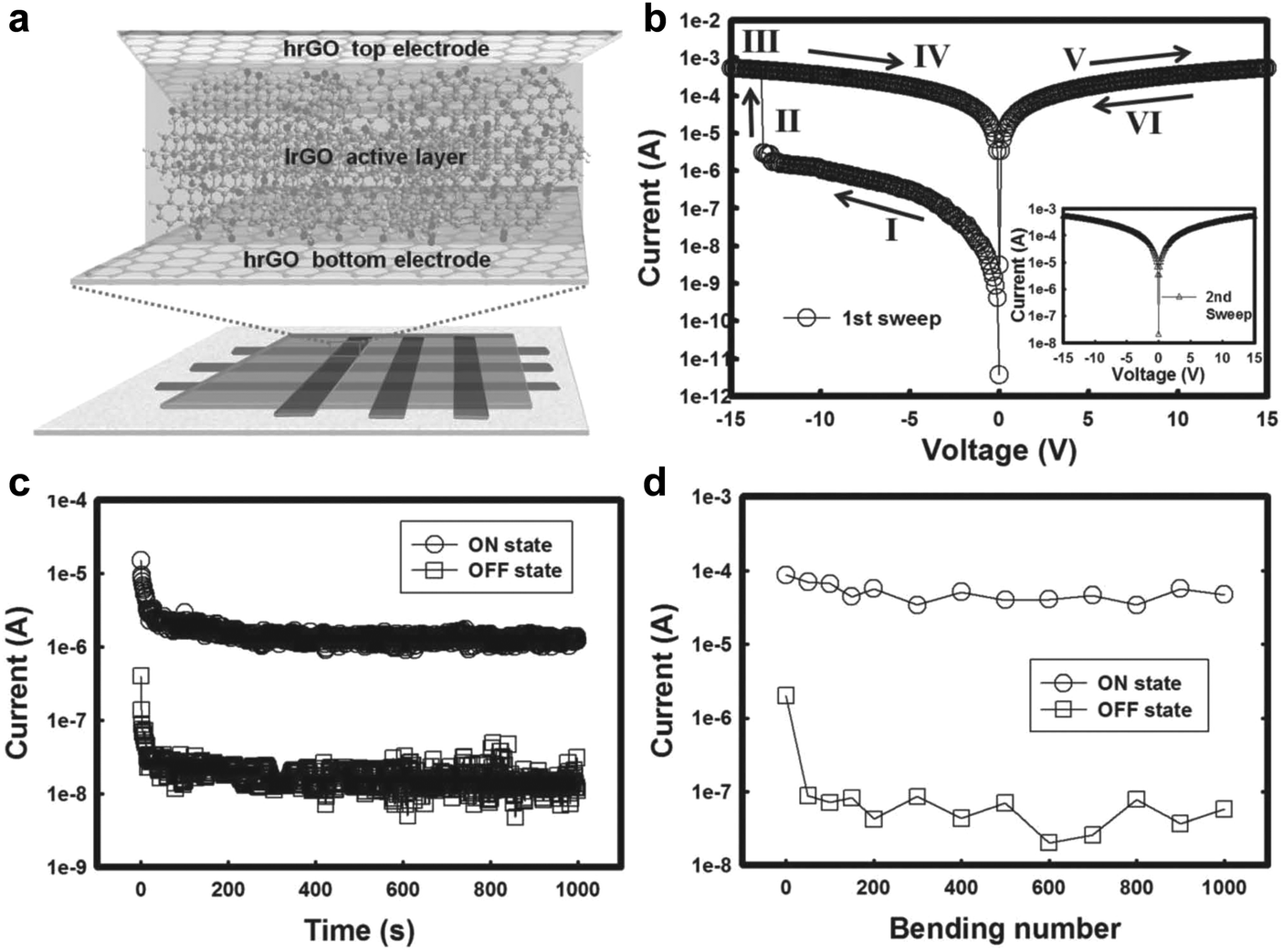 | ||
| Fig. 6 (a) Schematic illustration of the fabricated all-rGO memory device. (b) I–V characteristics of the WORM device in the 1st sweep and the 2nd sweep (inset). (c) Retention test of the memory device at a reading voltage of 1 V at ambient conditions. (d) Bending experiment of the all-rGO memory device at a voltage of 2 V. Reproduced with permission from ref. 39. Copyright 2013, John Wiley & Sons, Inc. | ||
Inspired by the aforementioned flexible all-rGO resistive memory device, recently our group developed a prototype of an all-carbon flexible, wearable, fiber-shaped non-volatile memory device,40 in which the conductive multi-walled CNT (MWCNT) microfibers were used as the electrodes and GO was employed as the active layer. Briefly, MWCNT microfibers were prepared from the grown spinnable MWCNT array (Fig. 7a). The GO sheets were then coated on the surface of the MWCNT fiber to form a core–shell hybrid fiber, referred to as MWCNT@GO (Fig. 7b). A flexible, all-carbon, wearable fiber-based resistive memory device was successfully fabricated by simply cross-stacking two MWCNT@GO fibers perpendicularly (Fig. 7b). It was found that the resultant device showed a WORM memory effect with high ON/OFF current of ∼103 (Fig. 7c–e), which is much higher than that of the aforementioned all-rGO based memory diode (102).39 The switching voltage of this device is around 3.5 V, which is much lower than that of the all-rGO based device (∼−13.2 V).39 Note that both of the two aforementioned all-carbon resistive memory devices exhibited a WORM type memory effect with high switching threshold voltage. Thus, the further optimization of device performance with tunable switching behavior is required.
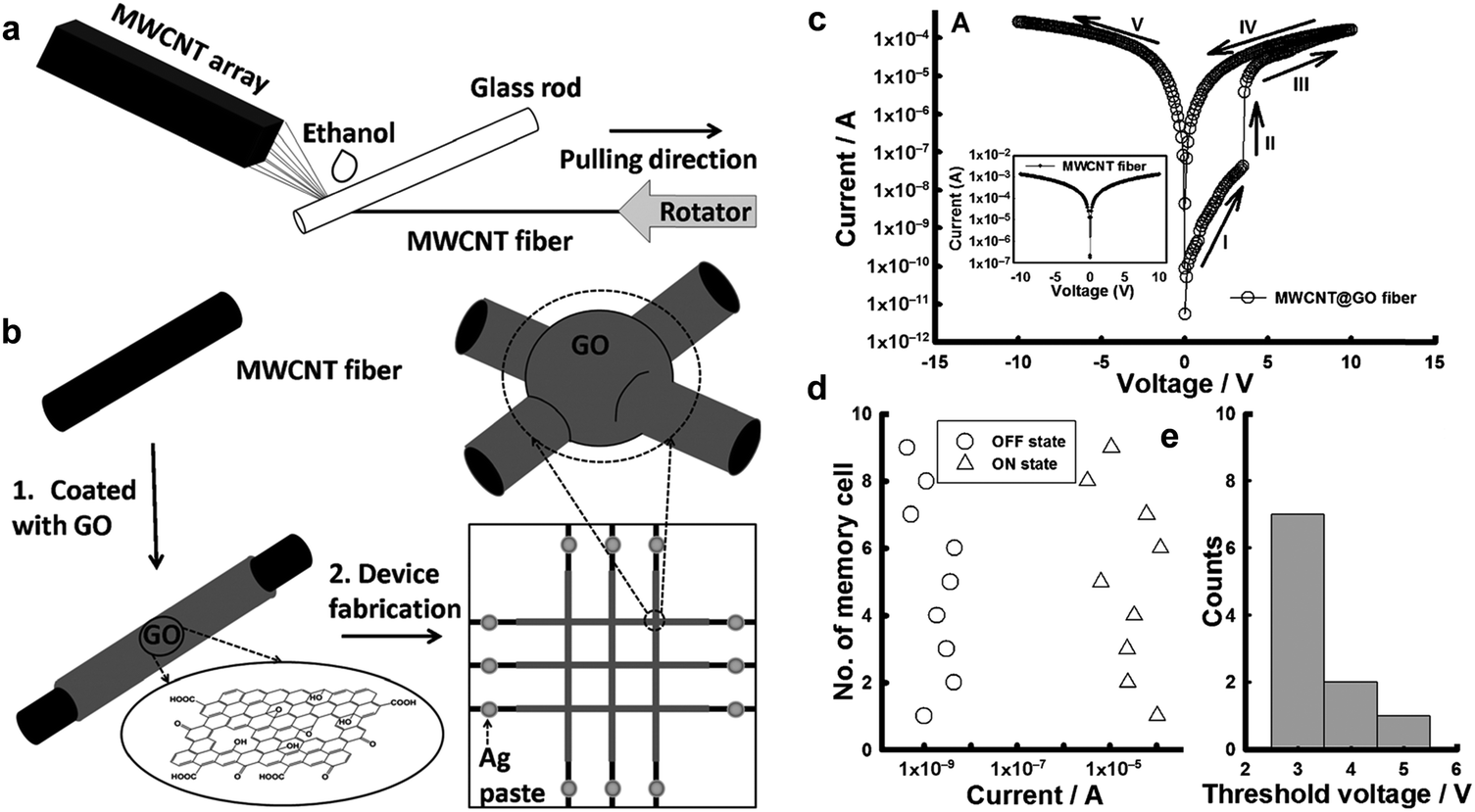 | ||
| Fig. 7 (a) Schematic illustration of preparation process for MWCNT fibers. (b) Schematic illustration of the fabrication of the MWCNT@GO fiber-based memory device. (c) The I–V characteristics of the MWCNT@GO fiber-based memory cell. The inset shows the I–V characteristic of the MWCNT fiber-based cell. (d) Statistical distribution of the ON- and OFF-state currents and (e) the threshold voltages of the operative MWCNT@GO fiber-based memory cells. Reproduced with permission from ref. 40. Copyright 2013, John Wiley & Sons, Inc. | ||
3. Non-volatile resistive memory devices based on 2D MoS2 nanosheets
Ultrathin 2D nanosheets of layered TMDs are the subject of intensive studies in the last few years.6,7 Among them, the MoS2 nanosheet has been extensively studied. Although it showed excellent performance in some electronic/optoelectronic devices (e.g. transistors and phototransistors), the MoS2 nanosheet exhibited no switching behavior when used as the active layer in a resistive memory device.41 Thus, the further functionalization of MoS2 nanosheets with other materials is indispensable to realize the electrical switching behavior.41 The summary and comparison of the MoS2 nanosheet-based non-volatile resistive memory devices is shown in Table 2.| Active layer materials | Electrodes | Technique for film fabrication | Memory effect | Switching voltage | ON/OFF current ratio | Stable retention time | Ref. |
|---|---|---|---|---|---|---|---|
| PVP-coated MoS2 sheets |
Top: Al
Bottom: rGO |
Spin-coating | Rewritable | ∼3.5 V | ∼102 | — | 42 |
| Mixture of MoS2 and GO sheets |
Top: Al
Bottom: ITO |
Spin-coating | Rewritable | <1.5 V | ∼102 | — | 44 |
| MoS2–P123 hybrid nanofibers |
Top: rGO
Bottom: rGO |
Spin-coating | Rewritable | 3–4 V | ∼5.5 × 10² | 4 × 10³ s | 45 |
| ZIF-8 coated MoS2 sheets |
Top: rGO
Bottom: rGO |
Spin-coating | WORM | ∼3.3 V | ∼7.0 × 10⁴ | 1.5 × 10³ s | 46 |
| MoOx/MoS2 hetero-structures |
Top: Ag
Bottom: Ag |
Spray-coating | Rewritable | 0.1–0.2 V | >106 | 104 s | 47 |
As a typical example, our group first demonstrated that the functionalization of MoS2 sheets with a commercial polymer, i.e. polyvinylpyrrolidone (PVP), could be easily achieved by direct exfoliation of MoS2 bulk crystals in PVP solution to form PVP-coated MoS2 sheets (MoS2–PVP), which was then used as the active layer in a flexible resistive memory device.42 Note that the highly conductive rGO film deposited on PET was used as the bottom electrode, and then the as-prepared MoS2–PVP hybrid nanosheets were deposited on it to form a thin film as the active layer by a simple spin-coating process. Al was deposited on MoS2–PVP film as the top electrode by the thermal evaporation technique. It was found that the obtained device with configuration of PET/rGO/MoS2–PVP/Al displayed a typical non-volatile flash memory effect. Its switching voltage was ∼3.5 V and its ON/OFF current ratio was ∼102 (Fig. 8a). The dielectric PVP coated on MoS2 played a crucial role in the device. According to the experimental I–V curves and fitted data, the electrical switching effect can be attributed to the charge trapping and detrapping behavior of MoS2 in PVP. Recently, a ternary hybrid nanomaterial comprising of PtAg NP-decorated MoS2 nanobelts coated with PVP, referred to as PtAg–MoS2@PVP, was synthesized and used as the active layer in a memory device.43 The resultant device with a configuration of Al/PtAg–MoS2@PVP/ITO/glass exhibited a DRAM effect, which is much different from the flash type memory device based on the MoS2–PVP composite.42 Note that the memory state cannot be stored when the power is switched off, suggesting its volatile nature rather that non-volatile. As another example, our group recently reported that by simply spin-coating the mixture of MoS2 and GO sheets to form a hybrid film which was used as the active layer, a memory device with the structure of ITO/MoS2–GO/Al was successfully fabricated.44 The resultant memory device also exhibited a rewritable switching effect with a switching voltage less than 1.5 V and an ON/OFF ratio of ∼102 (Fig. 8b). In this device, the insulating GO sheet acted as the dielectric material for the charge trapping and detrapping behavior of MoS2 sheets. Very recently, our group reported the integration of a flexible memory device based on the chiral nanofibers assembled from MoS2 nanosheets and Pluronic P123, an achiral triblock copolymer (PEO20PPO70PEO20), in which highly conductive rGO films were used as both bottom and top electrodes (Fig. 9a).45 Note that the device fabrication process is similar to that for fabrication of the aforementioned all-rGO memory device.39 The resultant device with a configuration of PET/rGO/MoS2–P123 nanofibers/rGO also revealed a rewritable memory effect with an ON/OFF current ratio of ∼5.5 × 10² (Fig. 9b). It did not show obvious degradation even after more than 50 consecutive cycles, indicating the high reproducibility of the device (Fig. 9c). No obvious fluctuation was detected on the ON/OFF ratio of the device even after a test period of more than 4 × 10³ s (Fig. 9d), indicating its excellent reliability. It is suggested that the excellent memory performance of the device is attributed to the highly ordered structure and the homogenous hybridization of MoS2 with P123.
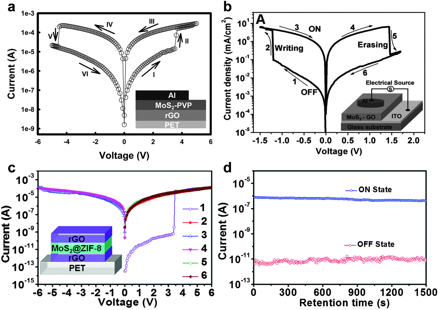 | ||
| Fig. 8 (a) I–V characteristics of the MoS2–PVP based flexible memory device. The inset shows the schematic illustration of the memory device. Reproduced with permission from ref. 42. Copyright 2012, John Wiley & Sons, Inc. (b) I–V characteristics of the MoS2–GO based memory device. The inset shows the schematic illustration of the memory device. Reproduced with permission from ref. 44. Copyright 2013, John Wiley & Sons, Inc. (c) I–V characteristics of the MoS2@ZIF-8 based flexible memory device. The inset shows the schematic illustration of the memory device. (d) The retention-ability test of the memory device at a reading voltage of 0.5 V in the ON and OFF states. Reproduced with permission from ref. 46. Copyright 2014, American Chemical Society. | ||
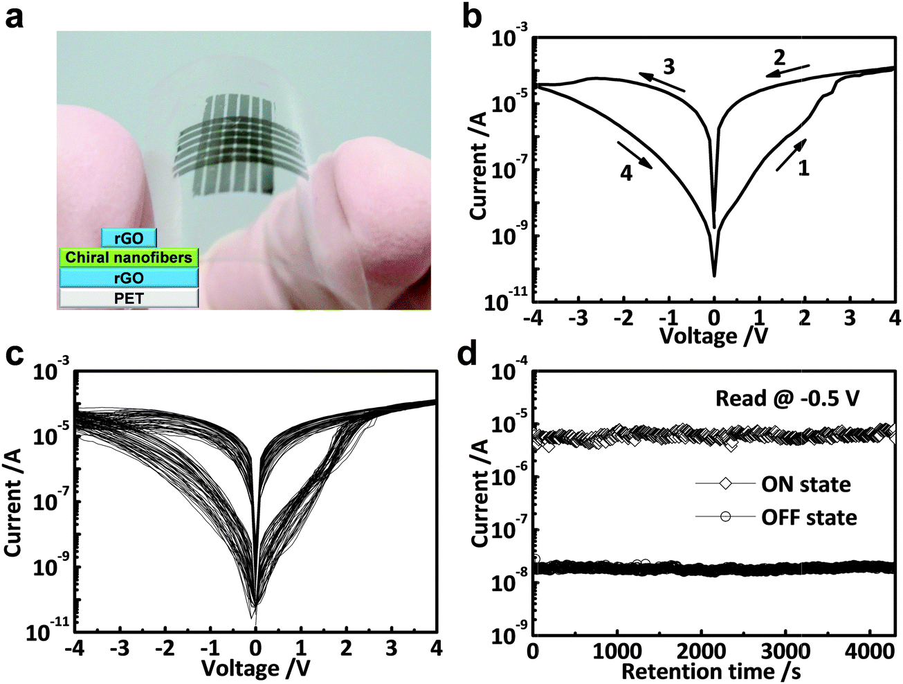 | ||
| Fig. 9 (a) Photograph of 6 × 6 flexible memory devices on PET. The inset shows the schematic illustration of the fabricated memory cell. (b) The first I–V characteristics of the MoS2–P123-based memory device. (c) Consecutive I–V measurements of the MoS2–P123-based memory cell. (d) Retention test of the MoS2–P123-based memory device read at −0.5 V under ambient conditions. Reproduced with permission from ref. 45. Copyright 2015, American Chemical Society. | ||
Besides non-volatile flash memory devices, other types of switching behaviors based on MoS2 nanosheets have also been achieved. Recently, our group demonstrated that the metal–organic framework (MOF)-coated MoS2 hybrid nanosheets could be used as the active layer in a memory device.46 First, the MoS2@zeolitic imidazolate frameworks (i.e. ZIF-8) core–shell hybrid nanostructures were prepared by simply mixing the aqueous solution of 2-methylimidazole and zinc acetate in the presence of MoS2 sheets with mild shaking and followed by an undisturbed reaction for 2 h. The hybrid core–shell nanostructures were then integrated into the memory as the active layer via a simple spin-coating process, where the patterned highly conductive rGO films were used as both bottom and top electrodes. The I–V characteristics revealed a typical WORM switching behavior of this device with a long retention time (>1500 s) (Fig. 8c and d). An ON/OFF ratio of as high as 7.0 × 10⁴ was realized, which is much higher than the aforementioned MoS2 nanosheet-based flash memory devices.42,44,45
As another example, Bessonov and coworkers fabricated flexible, full solution-processed printable non-volatile memory devices based on TMD-metal oxide hetero-structures very recently (Fig. 10a and b).47 Briefly, the bottom electrode was deposited on a plastic poly(ethylene naphthalate) (PEN) foil by using screen printing or ink-jet printing of commercial Ag NPs. Thin films comprising few-layered TMD nanosheets, i.e. MoS2 and WS2, were then deposited on the bottom electrode via a modified Langmuir–Blodgett method, which is also referred to as the spreading technique. After deposition of TMD thin film, the oxidation of the surface of TMD film is essential for the formation of hetero-structures, which is performed on a hot plate in air at 150–200 °C with subsequent rapid cooling. As an alternative, the oxidation can also be realized by using a photonic flash oxidation in air. It is worth pointing out that the thickness of the oxide layer is less than 3 nm. Impressively, the resistive memory device with a configuration of MoOx/MoS2 hetero-structure sandwiched by two printed Ag electrodes exhibited a typical flash type memory effect with ultra-low switching voltage (0.1–0.2 V) (Fig. 10c and d), which is much lower than that of all the previously reported MoS2 nanosheet-based resistive memory devices (1–4 V).42,44–46 Its ON/OFF current ratio is up to ∼106, that is best among all MoS2 nanosheet-based memory devices (102–105),42,44–46 resulting in less misreading during the reading and writing processes. The retention test revealed that no obvious degradation was observed even after 104 s (Fig. 10e), indicating the excellent reliability of the device. The excellent durability of the diode is evidenced by the maintenance of critical resistance over 104 bending cycles (Fig. 10f). It was believed that the thin MoOx layer played a crucial role in governing the switching behavior of the device, while the MoS2 layer was proved to have no significant impact on the key performance characteristics and only served as a mechanical support smoothing the rough Ag surface. Moreover, the WOx/WS2 hetero-structure based memory diode exhibited an almost identical memory effect and performance47 due to its similar structure and electronic properties with MoOx/MoS2. The ultra-low switching voltage, high ON/OFF current ratio, long retention time of the TMD-metal oxide hetero-structure based non-volatile resistive memory devices make them very promising in future electronics for fabrication of the next-generation flexible, printable, solution-processed resistive data storage devices.
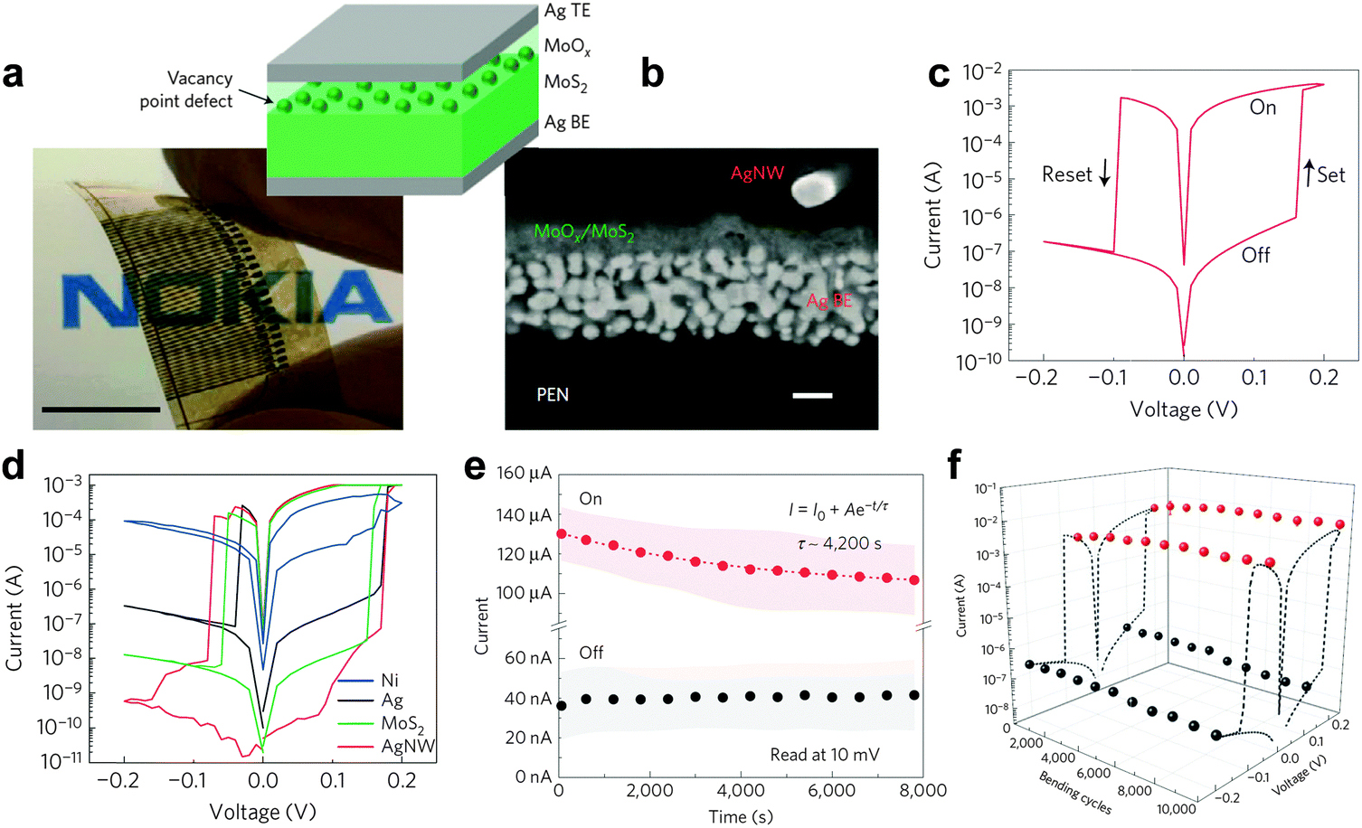 | ||
| Fig. 10 (a) Photograph of a cross-point memristor array on PEN. The inset shows a schematic of the Ag/MoOx/MoS2/Ag memristor. (b) Cross-section scanning electron microscopy (SEM) image of the Ag/MoOx/MoS2 device. (c) Typical I–V curve of a MoOx/MoS2 memristor. (d) Tailoring the I–V characteristics using various top electrode materials. (e) On and off state retention characteristics of the MoOx/MoS2 device recorded at +0.01 V. (f) Sustainability of Ioff (0.1 V, −0.2 V) and Ion (0.2 V, −0.05 V) with repeated bending up to a radius of curvature of 10 mm. Reproduced with permission from ref. 47. Copyright 2015, Nature Publishing Group. | ||
4. Conclusion and outlook
In this tutorial review, we summarized the recent progress in the fabrication of non-volatile resistive memory devices based on ultrathin 2D nanomaterials with particular focus on solution-processed ones, such as GO/rGO, functional GO/rGO composites, and MoS2 nanosheet-based composites, which hold great promise as the active layers in the next-generation information storage devices. The abundant members in the family of 2D nanomaterials and varying electronic properties allow us to engineer devices with desired electrical switching behaviors (e.g. WORM and flash) with superior performances, such as a high ON/OF current ratio, long retention time, low switching voltages and excellent reproducibility. To be able to play different essential roles in memory devices, all-carbon resistive memory devices have been successfully constructed based on rGO sheets. The high flexibility, transparency and excellent film formation ability of these ultrathin 2D nanomaterials offer the great possibility to fabricate flexible and transparent devices. Moreover, the solution processability of these 2D nanomaterials makes it possible to assemble full-solution processable, non-volatile memory devices via simple solution processing methods.Although many memory devices based on ultrathin 2D nanomaterials have been fabricated and studied, challenges still remain in device engineering for performance enhancement and mechanism understanding of the switching operation. Most of the studies focused only on the fabrication of 2D nanomaterial-based non-volatile resistive memory devices without too much concern on optimizing the device performance. For example, the performance of all-rGO non-volatile memory device is relatively poor (its switching voltage is as high as ∼−13.2 V).39 One of the challenges lies in how to achieve excellent device performance via engineering the active layer and/or electrodes since both of them are critical in determining the device performance. Moreover, although various electrical switching behaviors have been achieved based on solution-processed ultrathin 2D nanomaterials, the intrinsic operating mechanism was rarely fully explored. To understand the switching mechanism of the fabricated memory devices is very important to guide the design of high-performance devices in the future. Another main challenge remaining in this field is to develop effective and reliable techniques to figure out the switching mechanism of memory devices based on solution-processed ultrathin 2D nanomaterials.
It should be noted that many factors are important in the design of high-performance non-volatile memory devices based on ultrathin 2D nanomaterials. For example, the amount of functional groups on 2D nanosheets (e.g. GO) could affect the device performance. As summarized in Tables 1 and 2, even using the same material as the active layer, the ON/OFF current ratio, retention time and switching voltage of these devices are different from each other since they can also be affected by the electrodes and the thickness of the active layer. In addition, the device performance can be easily tuned by using different materials as active layers with varying electronic properties (Tables 1 and 2). Moreover, the switching behavior of a memory device can also be engineered by simply changing the ratio of hybridized materials in active layers. Therefore, systematic studies need to be carried out in order to optimize all these factors, including the surface functional groups, electrodes used, thickness and hybridization with other materials of the active layers, to realize high-performance non-volatile memory devices based on ultrathin 2D nanomaterials.
Admittedly, the current research on solution-processed ultrathin 2D nanomaterials for non-volatile resistive memory devices is still in its early stage. Although many devices have been successfully constructed, the device performance, including the ON/OFF current ratio, cycling performance, retention time and switching voltage, is far from the criteria of practical data storage technology.2 One of the future research directions is to engineer the device performance of ultrathin 2D nanomaterial-based resistive memory devices and thus to meet the criteria for real data storage devices. Besides, most of the ultrathin 2D nanomaterials used for fabrication of resistive memory devices are graphene and MoS2 or their composites. It is noteworthy that there are many other solution-processed ultrathin 2D nanomaterials, such as other TMDs (e.g. TiS2, TaS2, WS2 and MoSe2), hexagonal boron nitride (h-BN), transition metal carbides, metals (e.g. Au, Pd and Rh), black phosphorus and MXenes.48,49 The physical and electronic properties of these ultrathin 2D nanomaterials are different from each other. More importantly, a host of functional hybrid nanomaterials based on ultrathin 2D nanomaterials with different electronic properties has been prepared.50 Bearing this in mind, one of the most promising directions in this field is to integrate these ultrathin 2D nanomaterials and their composites to resistive memory devices, and then investigate their electrical switching behaviors and mechanisms.
Acknowledgements
This work was supported by MOE under AcRF Tier 2 (ARC 26/13, No. MOE2013-T2-1-034), AcRF Tier 1 (RG 61/12, RGT18/13, and RG5/13), Start-Up Grant (M4080865.070.706022), and Singapore Millennium Foundation in Singapore. This research is also conducted by NTU-HUJ-BGU Nanomaterials for Energy and Water Management Programme under the Campus for Research Excellence and Technological Enterprise (CREATE), which is supported by the National Research Foundation, Prime Minister's Office, Singapore.References
- A. K. Sharma, Advanced Semiconductor Memories: Architectures, Designs and Applications, Wiley-IEEE, Piscataway, NJ, 2003 Search PubMed.
- J. C. Scott, Science, 2004, 304, 62–63 CrossRef CAS PubMed.
- T. W. Kim, Y. Yang, F. S. Li and W. L. Kwan, NPG Asia Mater., 2012, 4, e18 CrossRef.
- K. S. Novoselov, A. K. Geim, S. V. Morozov, D. Jiang, Y. Zhang, S. V. Dubonos, I. V. Grigorieva and A. A. Firsov, Science, 2004, 306, 666–669 CrossRef CAS PubMed.
- M. J. Allen, V. C. Tung and R. B. Kaner, Chem. Rev., 2010, 110, 132–145 CrossRef CAS PubMed.
- M. Chhowalla, H. S. Shin, G. Eda, L. J. Li, K. Loh and H. Zhang, Nat. Chem., 2013, 5, 263–275 CrossRef PubMed.
- X. Huang, Z. Y. Zeng and H. Zhang, Chem. Soc. Rev., 2013, 42, 1934–1946 RSC.
- V. Nicolosi, M. Chhowalla, M. G. Kanatzidis, M. S. Strano and J. N. Coleman, Science, 2013, 340, 1226419 CrossRef.
- Y. Jing, Z. Zhou, C. R. Cabrera and Z. Chen, J. Mater. Chem. A, 2014, 2, 12104–12122 CAS.
- Y. Chen, C. L. Tan, H. Zhang and L. Z. Wang, Chem. Soc. Rev., 2015 10.1039/C4CS00300D.
- Y. Chen, B. Zhang, G. Liu, X. D. Zhuang and E. T. Kang, Chem. Soc. Rev., 2012, 41, 4688–4707 RSC.
- C. L. He, F. Zhuge, X. F. Zhou, M. Li, G. C. Zhou, Y. W. Liu, J. Z. Wang, B. Chen, W. J. Su, Z. P. Liu, Y. H. Wu, P. Cui and R. W. Li, Appl. Phys. Lett., 2009, 95, 232101 CrossRef PubMed.
- H. Y. Jeong, J. Y. Kim, J. W. Kim, J. O. Hwang, J. E. Kim, J. Y. Lee, T. H. Yoon, B. J. Cho, S. O. Kim, R. S. Ruoff and S. Y. Choi, Nano Lett., 2010, 10, 4381–4386 CrossRef CAS PubMed.
- S. K. Hong, J. E. Kim, S. O. Kim and B. J. Cho, J. Appl. Phys., 2011, 110, 044506 CrossRef PubMed.
- M. D. Yi, L. T. Zhao, Q. L. Fan, X. H. Xia, W. Ai, L. H. Xie, X. M. Liu, N. E. Shi, W. J. Wang, Y. P. Wang and W. Huang, J. Appl. Phys., 2011, 110, 063709 CrossRef PubMed.
- F. Zhao, J. Q. Liu, X. Huang, X. Zou, G. Lu, P. J. Sun, S. X. Wu, W. Ai, M. D. Yi, X. Y. Qi, L. H. Xie, J. L. Wang, H. Zhang and W. Huang, ACS Nano, 2012, 6, 3027–3033 CrossRef CAS PubMed.
- S. Seo, Y. Yoon, J. Lee, Y. Park and H. Lee, ACS Nano, 2013, 7, 3607–3615 CrossRef CAS PubMed.
- W. P. Lin, S. J. Liu, T. Gong, Q. Zhao and W. Huang, Adv. Mater., 2014, 26, 570–606 CrossRef CAS PubMed.
- X. Y. Qi, C. L. Tan, J. Wei and H. Zhang, Nanoscale, 2013, 5, 1440–1451 RSC.
- G. Liu, X. D. Zhuang, Y. Chen, B. Zhang, J. H. Zhu, C. X. Zhu, K. G. Neoh and E. T. Kang, Appl. Phys. Lett., 2009, 95, 253301 CrossRef PubMed.
- X. D. Zhuang, Y. Chen, G. Liu, P. P. Li, C. X. Zhu, E. T. Kang, K. G. Neoh, B. Zhang, J. H. Zhu and Y. X. Li, Adv. Mater., 2010, 22, 1731–1735 CrossRef CAS PubMed.
- B. Zhang, G. Liu, Y. Chen, L. J. Zeng, C. X. Zhu, K. G. Neoh, C. Wang and E. T. Kang, Chem. – Eur. J., 2011, 17, 13646–13652 CrossRef CAS PubMed.
- C. X. Wu, F. S. Li, Y. C. Zhang, T. L. Guo and T. Chen, Appl. Phys. Lett., 2011, 99, 042108 CrossRef PubMed.
- B. Zhang, Y. L. Liu, Y. Chen, K. G Neoh, Y. X. Li, C. X. Zhu, E. S. Tok and E. T. Kang, Chem. – Eur. J., 2011, 17, 10304–10311 CrossRef CAS PubMed.
- C. H. Jin, J. Lee, E. Lee, E. Hwang and H. Lee, Chem. Commun., 2012, 48, 4235–4237 RSC.
- B. Zhang, Y. Chen, Y. J. Ren, L. Q. Xu, G. Liu, E. T. Kang, C. Wang, C. X. Zhu and K. G. Neoh, Chem. – Eur. J., 2013, 19, 6265–6273 CrossRef CAS PubMed.
- A. D. Yu, C. L. Liu and W. C. Chen, Chem. Commun., 2012, 48, 383–385 RSC.
- Q. Zhang, J. Pan, X. Yi, L. Li and S. M. Shang, Org. Electron., 2012, 13, 1289–1295 CrossRef CAS PubMed.
- P. Cui, S. Seo, J. Lee, L. Wang, E. Lee, M. Min and H. Lee, ACS Nano, 2011, 5, 6826–6833 CrossRef CAS PubMed.
- L. Valentini, M. Cardinali, E. Fortunati and J. M. Kenny, Appl. Phys. Lett., 2014, 105, 153111 CrossRef PubMed.
- X. Huang, Z. Y. Zeng, Z. X. Fan, J. Q. Liu and H. Zhang, Adv. Mater., 2012, 24, 5979–6004 CrossRef CAS PubMed.
- S. T. Han, Y. Zhou and V. A. L. Roy, Adv. Mater., 2013, 25, 5425–5449 CrossRef CAS PubMed.
- J. Q. Liu, Z. Lin, T. Liu, Z. Y. Yin, X. Z. Zhou, S. Chen, L. H. Xie, F. Boey, H. Zhang and W. Huang, Small, 2010, 6, 1536–1542 CrossRef CAS PubMed.
- J. Q. Liu, Z. Y. Yin, X. H. Cao, F. Zhao, A. Ling, L. H. Xie, Q. L. Fan, F. Boey, H. Zhang and W. Huang, ACS Nano, 2010, 4, 3987–3992 CrossRef CAS PubMed.
- M. Min, S. Seo, S. M. Lee and H. Lee, Adv. Mater., 2013, 25, 7045–7050 CrossRef CAS PubMed.
- H. Tian, H. Y. Chen, T. L. Ren, C. Li, Q. T. Xue, M. A. Mohammad, C. Wu, Y. Yang and H. S. P. Wong, Nano Lett., 2014, 14, 3214–3219 CrossRef CAS PubMed.
- Y. S. Chen, Y. F. Xu, K. Zhao, X. J. Wan, J. C. Deng and W. B. Yan, Nano Res., 2010, 3, 714–721 CrossRef CAS PubMed.
- Y. F. Xu, Y. Wang, J. J. Liang, Y. Huang, Y. F. Ma, X. J. Wan and Y. S. Chen, Nano Res., 2009, 2, 343–348 CrossRef CAS PubMed.
- J. Q. Liu, Z. Y. Yin, X. H. Cao, F. Zhao, L. H. Wang, W. Huang and H. Zhang, Adv. Mater., 2013, 25, 233–238 CrossRef PubMed.
- G. Z. Sun, J. Q. Liu, L. X. Zheng, W. Huang and H. Zhang, Angew. Chem., Int. Ed., 2013, 52, 13351–13355 CrossRef CAS PubMed.
- C. L. Tan and H. Zhang, Chem. Soc. Rev., 2015 10.1039/c4cs00182f.
- J. Q. Liu, Z. Y. Zeng, X. H. Cao, G. Lu, L. H. Wang, Q. L. Fan, W. Huang and H. Zhang, Small, 2012, 8, 3517–3522 CrossRef CAS PubMed.
- X. Hong, J. Q. Liu, B. Zheng, X. Huang, X. Zhang, C. L. Tan, J. Z. Chen, Z. X. Fan and H. Zhang, Adv. Mater., 2014, 26, 6250–6254 CrossRef CAS PubMed.
- Z. Y. Yin, Z. Y. Zeng, J. Q. Liu, Q. Y. He, P. Chen and H. Zhang, Small, 2013, 9, 727–731 CrossRef CAS PubMed.
- C. L. Tan, X. Y. Qi, Z. D. Liu, F. Zhao, H. Li, X. Huang, L. Shi, B. Zheng, X. Zhang, L. H. Xie, Z. Y. Tang, W. Huang and H. Zhang, J. Am. Chem. Soc., 2015, 137, 1565–1571 CrossRef CAS PubMed.
- X. Huang, B. Zheng, Z. D. Liu, C. L. Tan, J. Q. Liu, B. Chen, H. Li, J. Z. Chen, X. Zhang, Z. X. Fan, W. N. Zhang, Z. Guo, F. W. Huo, Y. H. Yang, L. H. Xie, W. Huang and H. Zhang, ACS Nano, 2014, 8, 8695–8701 CrossRef CAS PubMed.
- A. A. Bessonov, M. N. Kirikova, D. I. Petukhov, M. Allen, T. Ryhänen and M. J. A. Bailey, Nat. Mater., 2015, 14, 199–204 CrossRef CAS PubMed.
- S. Z. Butler, S. M. Hollen, L. Y. Cao, Y. Cui, J. A. Gupta, H. R. Gutiérrez, T. F. Heinz, S. S. Hong, J. X. Huang, A. F. Ismach, E. Johnston-Halperin, M. Kuno, V. V. Plashnitsa, R. D. Robinson, R. S. Ruoff, S. Salahuddin, J. Shan, L. Shi, M. G. Spencer, M. Terrones, W. Windl and J. E. Goldberger, ACS Nano, 2013, 7, 2898–2926 CrossRef CAS PubMed.
- M. S. Xu, T. Liang, M. M. Shi and H. Z. Chen, Chem. Rev., 2013, 113, 3766–3798 CrossRef CAS PubMed.
- X. Huang, C. L. Tan, Z. Y. Yin and H. Zhang, Adv. Mater., 2014, 26, 2185–2204 CrossRef CAS PubMed.
| This journal is © The Royal Society of Chemistry 2015 |