
 Open Access Article
 This Open Access Article is licensed under a
 Creative Commons Attribution 3.0 Unported Licence
Nanoparticle characterization based on STM and STS
Shinya
Kano†
a,
Tsukasa
Tada
a and
Yutaka
Majima
*ab
aMaterials and Structures Laboratory, Tokyo Institute of Technology, Yokohama 226-8503, Japan. E-mail: majima@msl.titech.ac.jp
bDepartment of Printed Electronics Engineering, Sunchon National University, Sunchon 540-742, Republic of Korea
First published on 13th October 2014
Abstract
In this review, we describe recent progress made in the study of nanoparticles characterized by scanning tunneling microscopy (STM) and scanning tunneling spectroscopy (STS). Basic principles of STM measurements and single-electron tunneling phenomena through a single NP are summarized. We highlight the results of electrical and photonic properties on NPs studied by STM and STS. Because nanoparticles are single-digit nanometre in diameter, a single-electron transport on individual nanoparticles such as Coulomb blockade and resonant tunneling through discrete energy levels are investigated. Photon-emission from NPs is also introduced based on STM measurements. Novel single-nanoparticle functions such as stochastic blinking and one-write erasing behaviours are presented. This review provides an overview of nanoparticle characterization methods based on STM and STS that include the detailed understanding of the electrical and photonics properties of nanoparticles.
 Shinya Kano | Shinya Kano received his PhD degree from the Department of Materials Science and Engineering from Tokyo Institute of Technology (Tokyo Tech) in 2013. He was a visiting researcher in the Cavendish Laboratory, University of Cambridge, UK, in 2013. He has been an Assistant Professor in the Department of Electrical and Electronic Engineering, Kobe University, since 2014. His current research is on the application of functional nanomaterials to nanodevices. |
 Tsukasa Tada | Tsukasa Tada received the BS, MS, and PhD degrees in quantum chemistry from Kyoto University in 1973, 1975, and 1987, respectively. After joining the Toshiba R & D Center in 1975, he was with the VLSI Cooperative Laboratories from 1976 to 1980. Besides his research and development work in electron resist materials for VLSI, he has carried out quantum chemical studies on electronic materials, Si LSI device processing technology, and molecular devices at Toshiba R & D Center. He has been a research member of Tokyo Institute of Technology since 2014. Dr Tada is a member of the Chemical Society of Japan, the American Chemical Society, and the Japan Society of Applied Physics. |
 Yutaka Majima | Yutaka Majima received BS, MS and Dr of Engineering degrees from the Department of Electrical and Electronic Engineering from Tokyo Institute of Technology (Tokyo Tech), Japan, in 1987, 1989 and 1992, respectively. In 1992, he joined Toshiba Corporation, and became a Research Scientist in 1996. In 1996, he moved to Tokyo Tech as an Assistant Professor. He became an Associate Professor of the Department of Physical Electronics, Tokyo Tech in 1998. He has been Professor of Materials and Structures Laboratory, Tokyo Tech since 2009. His research covers nanoscale electronic devices and scanning tunneling microscopy. |
1 Introduction
Scanning tunneling microscopy (STM) is an indispensable technique in the current research fields of nanoelectronics and surface science.1–7,9–11 STM was developed by researchers Binnig and Rohrer, at the IBM Zurich Research Laboratory in 1982 to observe the (110) surfaces of CaIrSn4 and Au.1 STM has revealed many intriguing surface structures such as the 7 × 7 reconstruction of a Si(111) surface6 and highly oriented pyrolytic graphite (HOPG).7 Gaining atomic resolution in STM is a major motivation in surface science as the technique would allow researchers to obtain images of individual atoms and molecules in real space. Because of the molecular resolution, STM can display local electrical characteristics of nanomaterials by scanning tunneling spectroscopy (STS). The conductivity of a single nanomaterial particle such as carbon nanomaterials8,12–15 and organic molecules16–22 has been determined by STS.Colloidal synthesized nanoparticles (NPs) are interesting nanomaterials for future nanoelectronics and bioelectronics applications because of their unique electronic and optoelectronic properties.23–36 The electronic properties of NPs are strongly dependent on their size and ligand molecules. The size of NPs is typically in the nanometre scale, and determines the energy band.37,38 In the synthesis of NPs, the diameter can be precisely controlled to the sub-nanometre scale.39–50 Consequently, the bandgap of semiconductor NPs36,51,52 and mean energy level spacing53,54 can be tuned by the synthesis.24 A variety of chemical properties can be designed by selecting and controlling the ligand molecules surrounding the NPs. This surface functionalization is widely used for enhancing the solubility in a solvent or imparting chemical reactivity to the metallic surface.32,40,55 The synthesis of NPs has been established and the mass production of size-controlled NPs can be achieved. These advantages lead to practical applications for synthesized NPs in solid-state electronic devices.
Several applications for NPs have been reported: single-electron transistors (SETs),53,54,56–68 switches,31,69 and light-emitting diodes.31,70 To design nanodevices with NPs, it is necessary to evaluate the intrinsic properties of a single NP, such as the conductivity and quantum tunneling effect. STM and STS are the most suitable techniques to simultaneously obtain both a single-dot image and its electrical properties. Coulomb blockade phenomena71–85 and single-NP switching49,86,87 have been recently reported at room temperature (T ≈ 300 K) as well as low temperatures (T = 4.2–100 K). Therefore, it is important to understand what information of the synthesized NPs can be obtained from the STM and STS measurements.
Here, we review recent progress in the characterization of NPs based on STM and STS for applications of nanodevices. In Section 2, the basic principles of STM and STS are summarized to understand their advantages for this investigation. In Section 3, several types of synthesized NPs are reviewed. We also discuss established techniques to deposit NPs on a conductive substrate for STM analysis. In Section 4, we highlight the results of electrical and photonic characterization of NPs by STM and STS. Recent literature describing methods for obtaining useful functions of NPs and their ligands is also summarized.
2 Experimental background
2.1 Scanning tunneling microscopy
The atomic-resolution of STM is attributed to the imaging mechanism based on the quantum tunneling phenomena. STM measures the tunneling current I that is generated by a bias voltage V between the atomically sharp STM tip and the material surface. The tunneling current increases by an order of the current for every 1 Å reduction in distance.3,8 The distance in the xyz-directions is also controlled by a piezoelectric scanner, which provides angstrom-order changes in the distance, and a feedback loop, which controls the z-direction, is installed to keep the tunneling current constant. By observing the tunneling current as the tip scans a surface, the morphology of the surface can be precisely detected. Measurements can be carried out at room temperature in solution as well as at low temperature under ultra-high vacuum (UHV) conditions.9 We can obtain various electrical properties of an object by analyzing the tunneling current, such as the local density of states (LDOS) from dI/dV and local barrier height from dI/dz.3
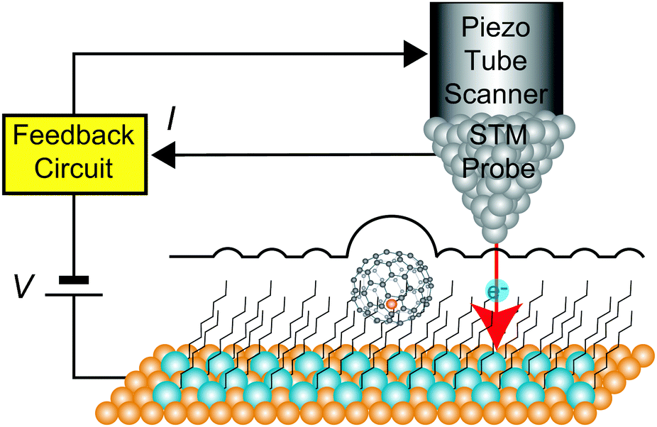
Fig. 1 shows a schematic view of scanning a metallofullerene and alkanethiol self-assembled monolayer (SAM) on an Au(111) surface by STM. Alkanethiol SAMs self-assemble on an Au(111) surface to form a  structure.15,88–91Fig. 2 shows the STM image of a Lu endohedral metallofullerene (Lu@C82) on an octanethiol SAM/Au(111) surface.15 The octanethiol molecules form SAMs on the Au(111) surface at a distance of 0.50 nm. It is noted that the corrugated surface of the metallofullerene reflects the LDOS in the molecule. The reason why the LDOS affects the STM topography images will be explained later.
 | ||
| Fig. 1 Schematic view of STM circuits in a constant-current mode. | ||
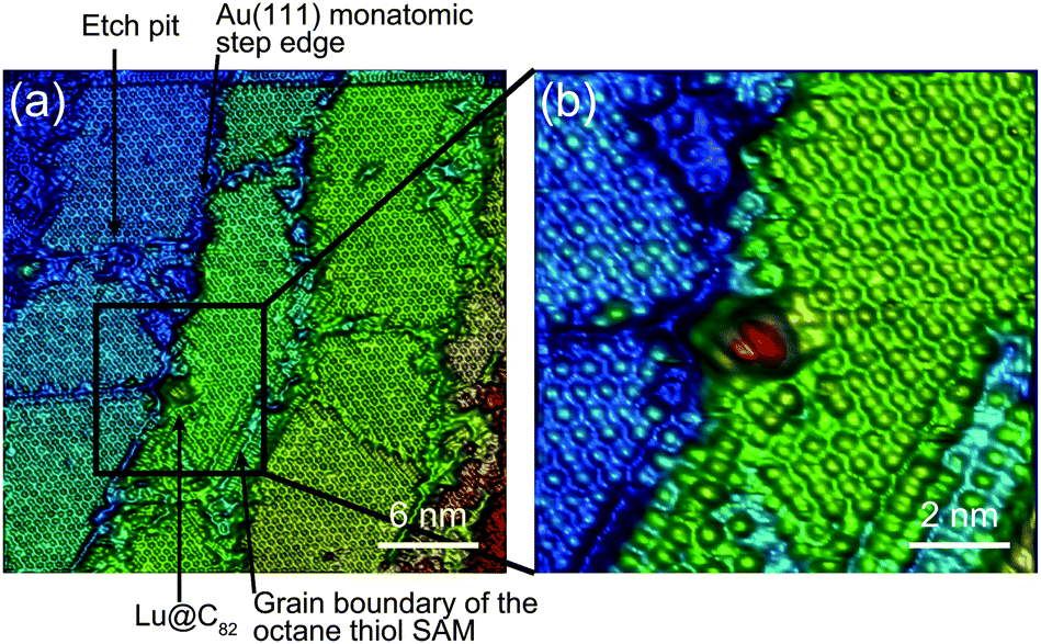 | ||
| Fig. 2 (a) and (b) Molecular-resolution 3D STM images of a Lu@C82 adsorbed on an octanethiol SAM/ an Au(111) surface at 65 K.15 Reprinted with permission from M. Iwamoto, D. Ogawa, Y. Yasutake, Y. Azuma, H. Umemoto, K. Ohashi, N. Izumi, H. Shinohara and Y. Majima, J. Phys. Chem. C, 2010, 114, 14704–14709. Copyright 2010 American Chemical Society. | ||
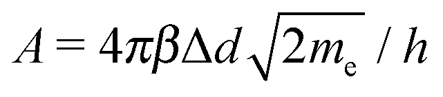
Here, we describe the basic physical principles of STM measurements. Fig. 3(a) shows a typical STM tunneling junction comprising alkanethiol molecules on an Au(111) surface. To elucidate the basic principles of STM measurements as simply as possible, we have introduced an approximation that the electric potential of an alkanethiol monolayer is nearly identical to that of the metal electrode (Au).92 By assuming this simple approximation, a schematic energy diagram of the STM junction can be illustrated as shown in Fig. 3(b).
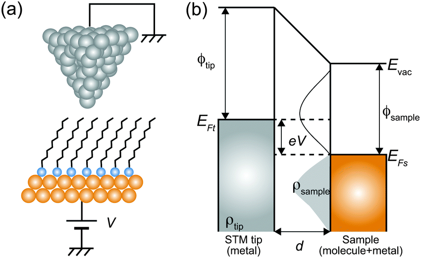 | ||
| Fig. 3 (a) Schematic illustration of an STM tunneling junction consisting of an alkanethiol SAM on an Au(111) surface. (b) Schematic energy diagram of the STM tunneling junction. Here, Evac is the vacuum energy level, EFt (EFs) is the Fermi energy of the tip (sample), ρtip (ρsample) is the density of states of the sample and the tip, ϕtip (ϕsample) is the work function of the tip (sample) metal, V is the applied sample bias voltage, and d is the distance from the sample to the tip. | ||
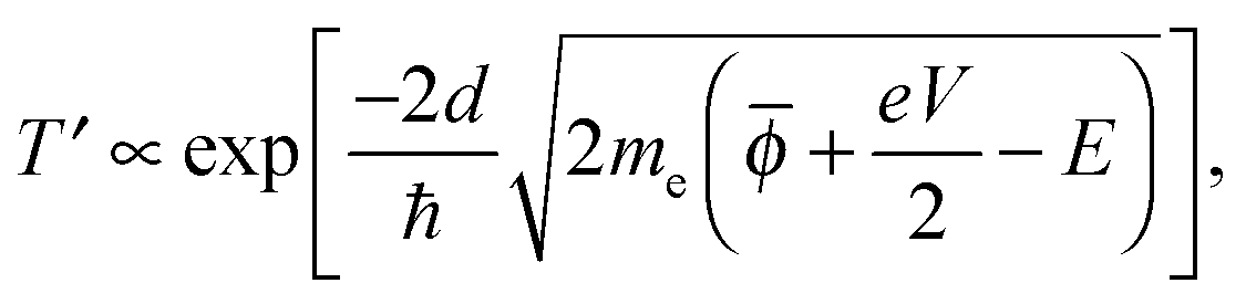
In this simple model, when a bias voltage V is applied between the tip and the metal electrode, the transmission coefficient T′ of the electrons through the potential barrier is approximated by the WKB approximation as93
 | (1) |
![[small phi, Greek, macron]](https://www.rsc.org/images/entities/i_char_e0d6.gif) = (ϕtip + ϕsample)/2 is the average potential barrier height between the tip and the sample, ℏ is the Dirac constant, and e is the elementary charge of an electron.
= (ϕtip + ϕsample)/2 is the average potential barrier height between the tip and the sample, ℏ is the Dirac constant, and e is the elementary charge of an electron.
If a hard wall potential barrier (i.e. infinite potential barrier = ∞) exists in the direction of the wave, the electron is completely reflected by the wall (T′ = 0). However, if a finite potential barrier exists ( ≠ ∞), there is some probability that the electron goes through the potential barrier even though the electron does not have enough energy to overcome the barrier (T′ ≠ 0).
The tunneling current can be obtained by the integration of the electron density ρ and the transmission coefficient T′,11
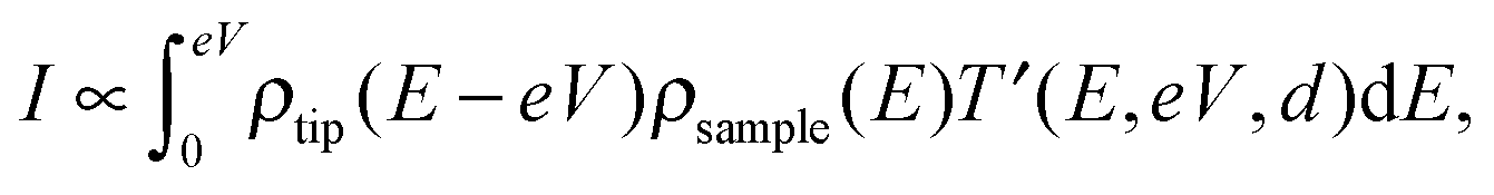 | (2) |
By considering the tunneling-distance dependence, the transconductance G of the material can be represented as follows,
G ∝ A![[thin space (1/6-em)]](https://www.rsc.org/images/entities/char_2009.gif) exp(−αz), exp(−αz), | (3) |
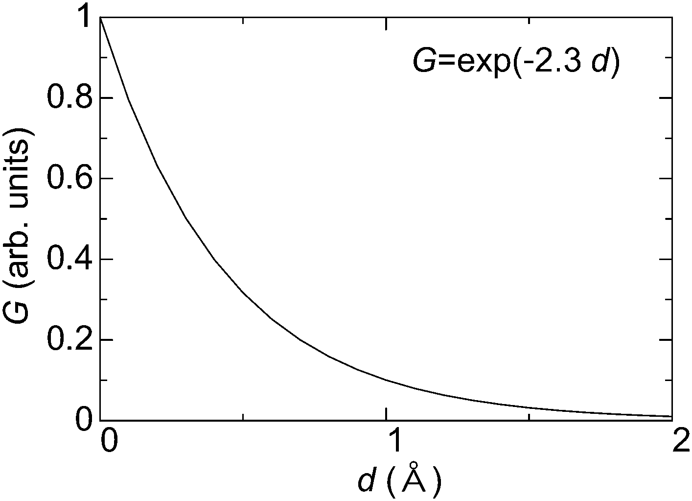 | ||
| Fig. 4 Typical relationship between transconductance (G) and thickness of materials (d) in a vacuum. | ||
The conductance of a single nanomaterial particle can be measured using STM by two methods. One is a break junction technique, which measures the conductance between the tip and the substrate while raising the tip.19,99–101 The peak conductance in the statistical histogram represents the conductance of a single molecule.
The other method is the STS technique for directly measuring the current–voltage (I–V) characteristics of a single molecule. In the investigation of a single NP, STS is usually adopted because single-electron tunneling phenomena can be simultaneously characterized in the current as a function of voltage. Therefore, we only consider the STS technique in further sections of this review.
2.2 Scanning tunneling spectroscopy
STS can achieve electrical characterization of a local point on a nanomaterial by monitoring the I–V characteristics. An STM tip is positioned over a sample keeping the feedback loop off during the measurements; therefore, the STS measurements can obtain the electrical characteristics of a truly single molecule or NP.If the tunneling current through the sample is represented by eqn (2), the value of dI/dV is given as follows,
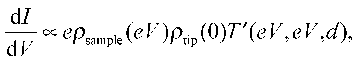 | (4) |
Electron tunneling is treated as an elastic process in the above discussion; however, a small amount of current is also provided by inelastic tunneling processes of electrons through the tunneling barrier. Vibrational modes of organic molecules can be detected by measuring dI2/dV2 characteristics using a lock-in amplifier, which is called inelastic tunneling spectroscopy (IETS).103–105 In IETS measurements, electrons release an energy of ℏω through the inelastic tunneling process as phonon vibrations ω of the nanomaterials. STM is also useful in nanophotonics to observe locally excited luminescence and plasmonic modes in nanostructures, as well as electrical characterization.106–108 In this case, the energy released from the tunneling electrons is converted into photonic energy, which excites photons from the nanomaterial. The simultaneous observation of topographies and photon-emission maps is realized by the combination of STM and an avalanche photodiode to count the number of photons.108 However, we can exclude the effects of inelastic tunneling processes in the STS measurements as long as the contribution of the inelastic tunneling process is small. Therefore, we keep two viewpoints in mind to analyze the STS characteristics: direct tunneling and single-electron tunneling.
, and (c) eV > , where the average barrier height of the insulator was .93 The three types of tunneling behaviors are shown in Fig. 5. When the temperature T = 0, the tunneling current density J can be written as| J = J0[ exp(−A½) − ( + eV)exp[−A( + eV)½]], | (5) |
 , J0 = e/(2πhΔd2β2), h is the Planck constant, Δd is the tunneling distance through an insulator, and β is a correction factor.
 | ||
| Fig. 5 Schematic energy band diagram of three types of tunneling behaviors in metal/insulator/metal structures: (a) eV ≃ 0, (b) eV > and (c) eV > . ϕ0 is the barrier height of the insulator is the average barrier height of the insulator. Δd is the tunneling distance of an electron and d is the thickness of the insulator. | ||
Characterization based on this basic analysis has been carried out to understand the electrical properties of organic molecules and nanogap electrodes.18,109–111 To understand the electrical behaviors, tunneling phenomena at the several-nanometre scale must be considered.
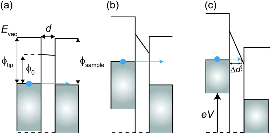
Typical experimental I–V characteristics of the DBTJ consisting of an STM tip/vacuum/octanethiol ligand/Au core/decanedithiol anchor molecule/Au(111) substrate are shown in Fig. 6 (solid line), which was measured by STS. A clear Coulomb staircase including Coulomb gap and first and second stairs for positive and negative bias voltages has been observed.
 | ||
| Fig. 6 Typical experimental I–V characteristic of the DBTJ consisting of an STM tip/vacuum/octanethiol ligand/Au core/decanedithiol anchor molecule/Au(111) substrate (solid line). An experimental Coulomb staircase is clearly observed. The dashed line represents the theoretical curve calculated by the orthodox theory. The inset is the schematic of the Coulomb blockade effect that is observed near V = 0. | ||
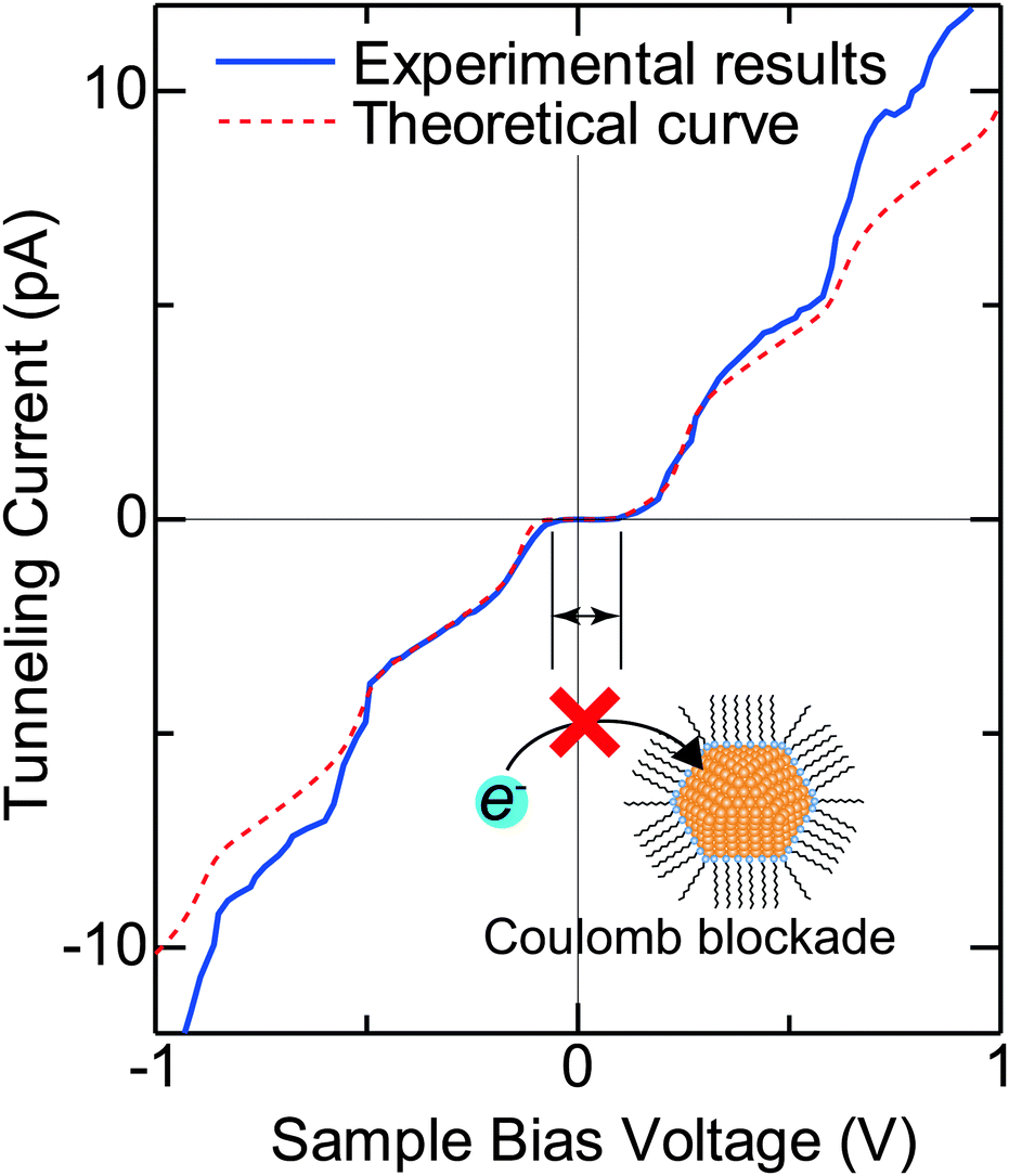
An equivalent circuit diagram of this DBTJ is shown in Fig. 7(b). Tunneling junction 1 (2) is expressed as a parallel of tunneling resistances R1 (R2) and capacitances C1 (C2), respectively. Here, we consider that junction 1 consists of a vacuum and ligand molecules, and junction 2 consists of only a decanedithiol.
 | ||
| Fig. 7 (a) Schematic image of DBTJs consisting of a single octanethiol protected Au nanoparticle on the Au(111) surface. (b) Equivalent circuits of the DBTJs. (c) and (d) Schematic energy band diagrams of DBTJs. (c) Coulomb blockade conditions. Electron tunneling is prohibited. (d) Allowed tunneling conditions because of sufficient energy (E+c) given by voltage. | ||
Single-electron tunneling can be described by the orthodox theory.81,112–114 A single electron can tunnel into the island when electrostatic conditions are present for the entire circuit; the total energy after changing the number of electrons in the island is smaller than the energy of the initial states. The change in the total energy when an electron tunnels through junction 1 ΔE±1 is given by
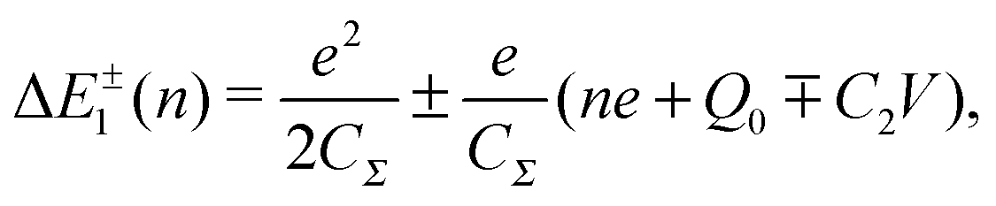 | (6) |
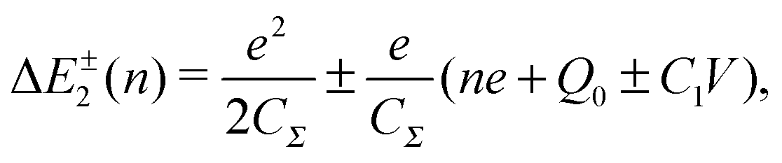 | (7) |
To observe the Coulomb blockade clearly, it is necessary to satisfy the energy-scale condition:
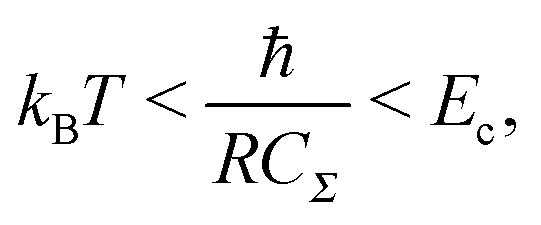 | (8) |
The tunneling resistance of R1 can be adjusted by a tunneling current through a DBTJ (set-point current). In contrast, the resistance of R2 is expected to be constant owing to the ligand molecules. The overall shape of the Coulomb staircase strongly depends on the tunneling resistance ratio R1/R2 as shown in Fig. 8; therefore, we can estimate the values of the tunneling resistance in the junctions.72,81,84,87 In evaporated Au NPs on dodecanethiol/Au(111) surfaces, it was reported that the total resistances (R1 + R2) and the total capacitances (C1 + C2) of DBTJs can be controlled by changing the set-point current in the STM system.72 The tunneling resistances in the DBTJs can be estimated as a unique value if 1 < R1/R2 < 50 when R1 is larger than R2.81 Under these conditions, we can estimate the resistance R2 between a NP and an Au(111) surface, which corresponds to the resistance of the linker molecules, by fitting the I–V curves with the orthodox theory.
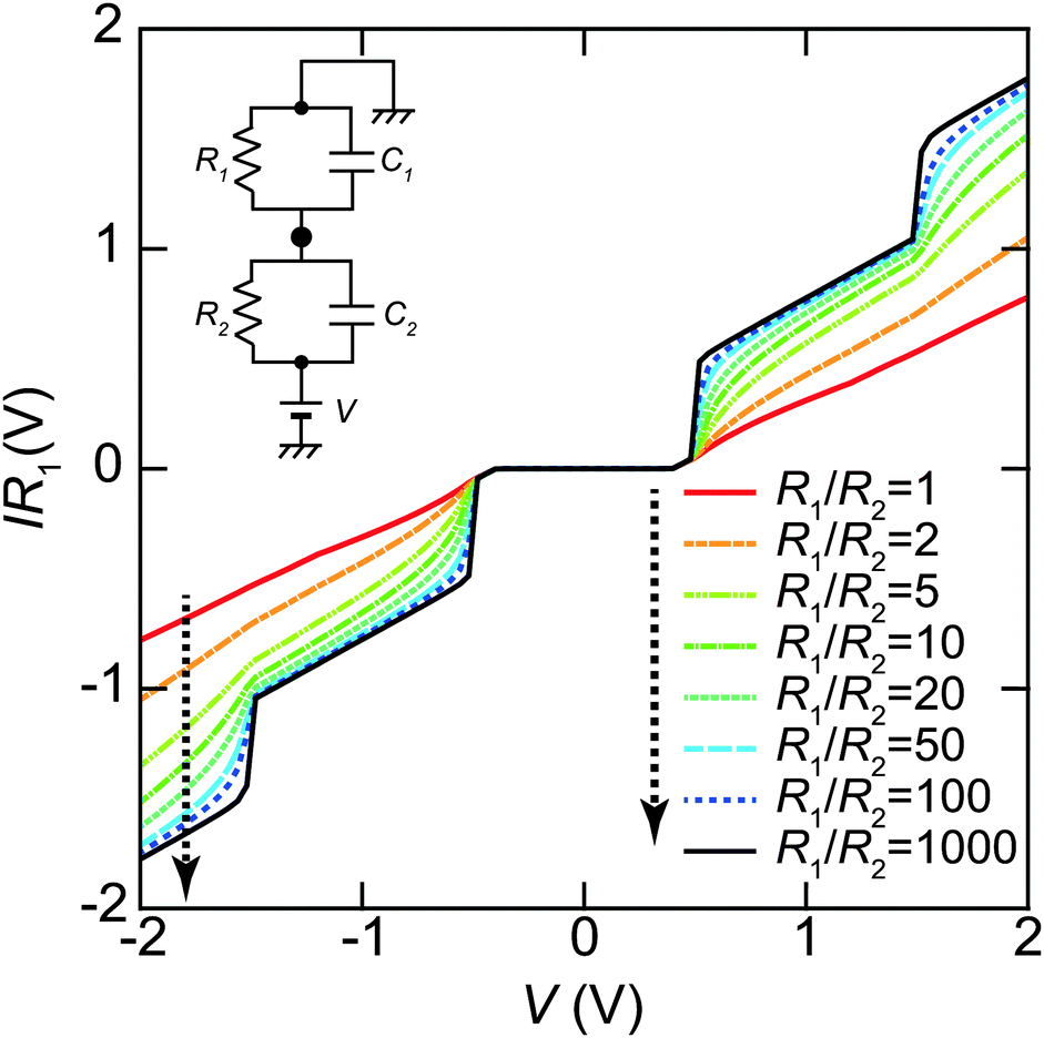 | ||
| Fig. 8 Set-point current dependence of the whole shape of Coulomb staircases. These curves are simulated by the orthodox theory81,114 using R1/R2 = 1, 2, 5, 10, 20, 50, 100 and 1000, respectively (indicated by the dashed arrow in this order). The circuit parameters are R1 = 0.1–100 GΩ, R2 = 0.1 GΩ, C1 = 0.16 aF, C2 = 0.20 aF, Q0 = 0e and T = 4.2 K. The vertical axis is normalized by multiplying R1 to compare the whole shape of the Coulomb staircase. A higher R1/R2 value gives a sharper Coulomb staircase; in contrast, the shapes of the curves are not dependent on R1/R2 values under R1/R2 > 50. | ||
One interesting application of a Coulomb blockade is a single-electron transistor, which comprises a DBTJ and gate electrodes capacitively coupled to a Coulomb island.115 Single-electron transistors can be used as single-electron memory,116 a single-electron pump,117 and multiple logic circuits.63 Room-temperature single-electron transistors have been reported using metallic NPs,58,59 Si NPs,118–121 and carbon nanotubes.122,123 The charging energy of a single-electron transistor is an important parameter to determine the operating temperature following eqn (8). We can evaluate the charging energy of a single NP by the STS measurement and the orthodox theory. Thus, STM and STS are useful tools to explore candidates for Coulomb islands in single-electron transistors.
2.3 Charging energy of nanoparticles
Here, we evaluate the charging energy of NPs to show that synthesized NPs are promising for practical applications of quantum effects. Fig. 9(a) shows the theoretical capacitance between a single conductive sphere and a conducting plate, which is proportional to the capacitance of a sphere in free space.124,125 The corresponding charging energy is estimated in Fig. 9(b). The charging energy increases as the size of the Coulomb island decreases. The simulated Ec/kBT dependence of the Coulomb staircase is shown in Fig. 9(c). The I–V curves are calculated by the orthodox theory and it is clear that this simulation follows eqn (8). Moreover, this simulation indicates that Ec is required to be much larger than a thermal fluctuation to observe a clear zero conductance region. The zero conductance region of the Coulomb blockade is critical to maintain the on/off ratio in a single-electron transistor. Therefore, Coulomb islands less than 2 nm in diameter are desired for room-temperature operation, e.g., Ec > 260 meV where Ec is 10 times larger than the thermal energy at 300 K.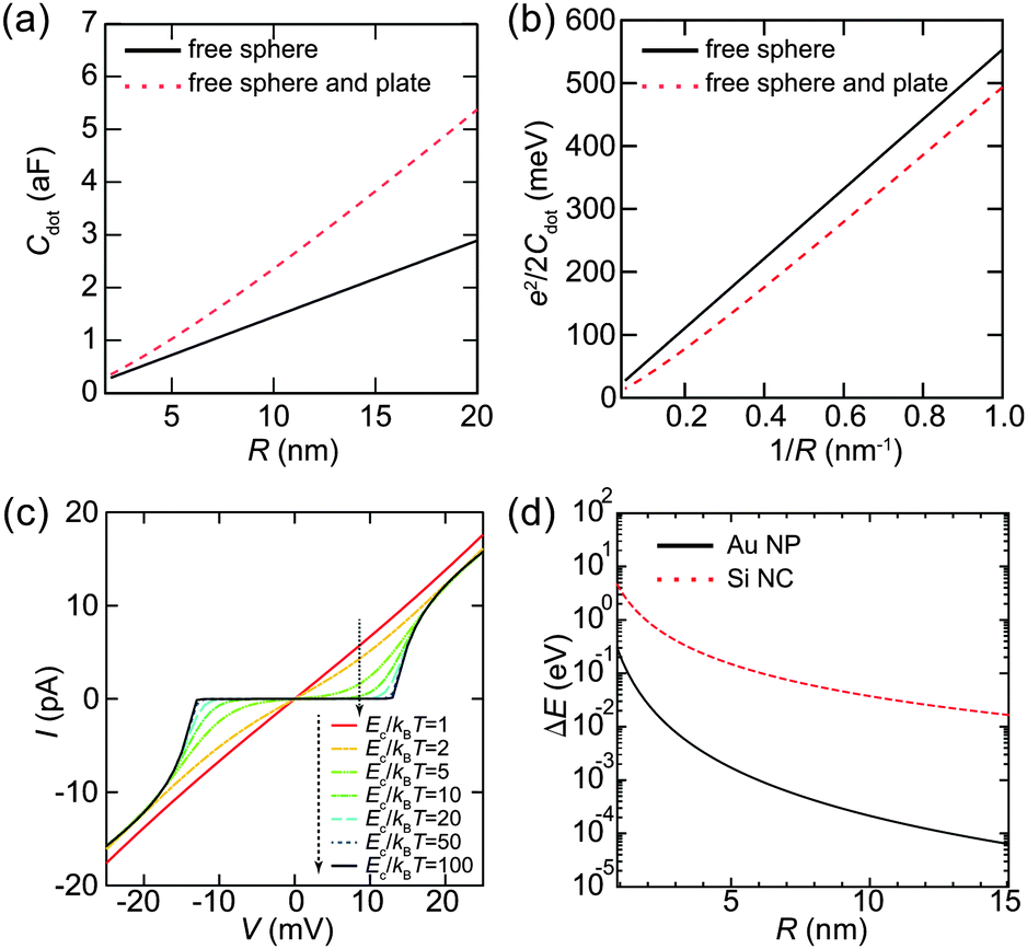 | ||
| Fig. 9 (a) Theoretical capacitances Cdot of a free sphere (solid lines), between a single conductive sphere and a conducting plate (dashed lines). (b) Corresponding charging energy Ec = e2/2Cdot of a free sphere (solid lines), between a single conductive sphere and a conducting plate (dashed lines). The value of a relative dielectric constant εr in alkanethiol (2.6) is used above calculations. (c) Simulated Ec/kBT dependence of Coulomb staircases. The values of Ec/kBT are 1, 2, 5, 10, 20, 50 and 100 in the order as indicated by the dashed arrow. The circuit parameters are, R1 = 1 GΩ, R2 = 0.1 GΩ, C1 = 6.0 aF, C2 = 6.0 aF, Q0 = 0e and Ec = 6.7 meV (comparable to a thermal energy at 77 K). (d) Calculated mean energy level spacing ΔE of Au NP and Si NC (nanocrystal). Here, R represents a diameter of NPs. | ||
When the diameter of NPs is lower than 2 nm, we need to consider the effect of the discrete 0D energy levels caused by quantum confinement, even at room temperature. Fig. 9(d) shows an example of the discrete energy level spacing ΔE in Au NPs and Si nanoclusters (NCs). The value of ΔE in the metallic Au NPs is directly derived from the density of states at the Fermi energy and volume ΔE ≈ 2π2ℏ2/(mAukFV), where mAu is the electron mass in Au (1.1 me) and kF is the Fermi wavenumber in Au.23,126 This assumption is valid when the Fermi level is in a half-filled band (i.e., metallic NPs), which implies that a number of electrons exist in the NPs. Therefore, the 0D levels are randomly dispersed along the energy axis, and the value of ΔE in metallic NPs describes a mean spacing between the levels.
In contrast, the value of ΔE in semiconductor NPs is estimated by the potential well of a quantum sphere ΔE ≈ π2ℏ2/(2mSi(R/2)2), where mSi is the electron mass in Si (0.40 me).127,128 This corresponds to an energy difference between the ground state and the first excited state of the classical quantum sphere model. Semiconductor NPs have a few electrons because the Fermi level is in its bandgap; thus, the 0D levels tend to follow the electron-shell filling described by the potential-well approximation. This simple 0D-level spectrum is attributed to the observation of a predictable atomic-shell filling in semiconductor NPs (shown later). Semiconductor NPs generally have larger energy spacings than metallic NPs of the same diameter.129 The condition to observe the effect of discrete energy levels is ΔE > 3.5kBT, which was derived from the thermal broadening of Fermi–Dirac distributions in metallic lead electrodes.130
To harness these quantum effects practically, it is critical to control the size of the Coulomb islands. Electron configurations of elemental atoms are precisely determined by the number of atomic nuclei. Coulomb islands of a single-donor atom in Si have been reported as single-atom transistors, which show a charging energy or resonant spectrum in accordance with the excited state of the single donor.131–133 These results indicate that precisely size-controlled Coulomb islands show reproducible quantum effects. Synthesized NPs have several advantages: size control in the sub-nanometre scale, ability for mass production, and reproducibility. Thus, synthesized NPs are promising materials to exhibit the above-mentioned quantum effects.
3 Synthesized nanoparticles
For stable metallic NPs, noble metals such as Au, Ag, and Pt are used because they are not easily oxidized.31 Synthesized NPs are usually surrounded by ligand molecules to prevent aggregation. One of the most famous techniques to synthesize metallic NPs is the Brust–Schiffrin method for Au NPs.40,43 Temperature- and air-stable, size-controlled Au NPs can be mass produced by this method and can be functionalized by ligand molecules.27,134–136 Teranishi et al. controlled the core diameter of decanethiol-protected Au NPs from 3.4 ± 0.3 nm to 6.8 ± 0.5 nm by revealing the appropriate heat-treatment temperatures during synthesis.45 The number of Pt atoms (13, 55, 147, 309, etc.)137,138 and Au atoms (10, 15, 18, 22, 25, etc.)48 occurs in the well-known magic numbers. As the magic number is determined by the crystalline structure of the NPs, the size of the nanoparticles can be identical. Therefore, if we utilize the magic number of atoms in single-electron devices, the charging energy of the Coulomb islands and the 0D-level spacing can be identical.Several thiol-derivatized molecules are used as ligands, the same as alkanethiol molecules, such as amino-type molecules,46 glutathione thiolate,47,48 porphyrin,49 and oligo(phenylene-ethynelene) (OPE) molecules.50 The synthesized NPs can be stored in the solid state under ambient conditions and redissolved in common organic solvents. Semiconductor NPs can also be synthesized by established methods to fine-tune the diameter in the sub-nanometre scale.51,52,55,139–142 Because of these advantages, synthesized NPs are intensively used in the field of nanoelectronics. Reported synthesized NPs are summarized in Table 1.
| Elements | Ligands | R (nm) | Ref. |
|---|---|---|---|
| N/A: not mentioned in the paper. | |||
| Au | CH3(CH2)9SH | 2.0–2.5 ± 1.0 | 40 |
| Pt | Phenanthroline, O2 | 1.5–2.5 | 39, 137, 177 |
| Au | Phosphine, Cl | 1.4 | 39 |
| Pd | Poly(N-vinyl-2-pyrrolidone) | 2.2 ± 0.4 | 143 |
| Au | CH3(CH2)11SH | 3.4 ± 0.3 | 45 |
| Au | CH3(CH2)5SH, HS(CH2)6SH | 2.2 | 42 |
| Au | CH3(CH2)11SH | 2.1 ± 0.3 | 144 |
| Ag | CH3(CH2)11SH | 5.5 ± 0.3 | 144 |
| Pd | CH3(CH2)11SH | 6.3 ± 0.4 | 144 |
| Au/Ag alloy | CH3(CH2)11SH | 3.8 ± 0.2 | 144 |
| Co | CH3(CH2)11COOH | 5.5 ± 1.0 | 194 |
| Au | CH3(CH2)17SH | 0.8 ± 0.2 | 44 |
| N,N-dimethylaminoethanethiol | |||
| Mercaptoethanesulfonic acid | |||
| Au or Ag | CH3(CH2)7SH and HOOCCH3(CH2)2SH | 3.7 | 217 |
| Au | C60 | 2 | 136 |
| Pd | Polyvinylpyrrolidone | 2.5 | 185 |
| Au | Polyvinylpyrrolidone | 1.7 | 185 |
| Au | Amino-type molecule | 2.4 ± 0.2 | 46 |
| Au | Glutathione | 0.7 | 48 |
| Au | Thiol-derivatized OPE | 1.7 ± 0.3 | 49 |
| Au | Thiol-derivatized porphyrin | 1.1 ± 0.2 | 50 |
| CdS, CdSe, CdTe | Trioctylphosphine | 3.7 ± 0.2 | 139 |
| Trioctylphosphine oxide | |||
| InP | Trioctylphosphine | 2.6–4.6 | 142 |
| Trioctylphosphine oxide | |||
| GaP | Trioctylphosphine | 3.0 | 142 |
| Trioctylphosphine oxide | |||
| InAs | Trioctylphosphine | 2.5–6.0 ± 10% | 141 |
| CdS | N/A | 2.1 ± 0.3% | 165 |
| CdSe | Trioctylphosphine oxide | 5 ± 0.5 | 201 |
| Hexadecylamine | |||
| PbSe | Oleic acid | 3 ± 0.3 | 201 |
The deposition of synthesized NPs is important in the practical application of NPs; such deposition is classified into two types of absorption: physisorption and chemisorption. Dropcast, spincoat, and Langmuir–Blodgett methods are widely used as physisorption processes to form monolayers of NPs on flat substrates. The interacting force between the NPs and the substrates is mainly caused by only van der Waals interactions. Conversely, chemisorption processes are based on chemical reactions between the NPs and the functionalized substrates with SAMs. The interacting forces in chemical interactions are stronger than van der Waals forces, which make the NPs stable on the substrates.
Controlling the density of NPs by the density of tether molecules on the substrate is a notable advantage in the chemisorption process. Alkanethiol–alkanedithiol-mixed SAMs can be formed by immersing Au(111) substrates into alkanethiol and alkanedithiol solutions successively.145–147 The inserted alkanedithiols in alkanethiol monolayers can be observed by STM or atomic force microscopy (AFM).83,145–147 In ref. 83, the density of chemisorbed Au nanoparticles was controlled in 1/100 × 100 nm2 in 0.5 mM octanedithiol solution and 39/100 × 100 nm2 in 50 mM solution. Electrically stable SETs (chemically assembled SETs) have been demonstrated by using the same chemisorption process to deposit a single synthesized Au NP between size-regulated nanogap electrodes formed by electroless-gold plating.54,60–65 Therefore, chemisorption is more promising than physisorption for stable and ideal electrical transport through the NPs by STM and STS.
In this section, we explained the advantages of the synthesized NPs. Chemical assembly processes are more suitable for stable chemisorption of NPs on a substrate.
4 Single-nanoparticle properties by scanning tunneling microscopy
4.1 Single-electron transport of single nanoparticles
In the early stages, single-electron transport in metallic NPs was mainly investigated by using STM. The NPs for STM investigation were made by thermal evaporation. Because metals naturally tend to nucleate into particles, a small amount of evaporation (less than 1 nm) can generate hemispherical NPs for small metal droplets on a thin insulator.148–150 In the first report of single-electron transport in NPs, a Coulomb staircase was observed at 4.2 K in a structure comprising a granular layer of evaporated Au NPs in the oxide layer between two Ag or Cu films.151 Because multiple current paths exist as parallel arrays of junctions when this technique is used, the observed Coulomb staircase strongly depends on the variation in size or the number of NPs. Therefore, it is necessary to observe single-electron transport in a single NP by using STM and STS measurements.A Coulomb staircase was first observed by STM in a structure comprising a granular Al layer on oxidized Al films.152 The measurement temperature was 1.2 K and STS was carried out on a single granular Al dot. The observed Coulomb staircase had a periodic structure, which was explained by Monte Carlo simulations based on the DBTJ of a single Coulomb island. This analysis proved that the single NP acted as a Coulomb island in this measurement. After this report, several evaporated NPs were investigated by STM and STS at low temperature, e.g., Al,153 Au,114,154,155 Co,156 In,157,158 Pt,159,160 Pd,161,162 and Si.79
To increase the observation temperature of the Coulomb blockade, it is necessary to form smaller NPs for Coulomb islands. To observe the Coulomb blockade at room temperature (T = 300 K), the charging energy needs to be much larger than the thermal fluctuation kBT (25.8 meV). We have shown in Fig. 9(c) that a much larger charging energy is required to observe single-electron transport without any random tunneling events. Therefore, the size of the NPs has to be on the order of 1 nm to observe the Coulomb blockade at room temperature.
Schönenberger et al. reported a Coulomb staircase on Au-evaporated NPs/ZrO2 (1 nm)/Au film at room temperature in air.71 The schematic image of the structure and STS characteristics are shown in Fig. 10(a) and (b), respectively. To increase the charging energy, the ideal height and diameter of the NPs were 0.2 nm and 4 ± 0.5 nm, respectively. The charging energy of the DBTJ was 70 meV, which is larger than 26 meV at 300 K; therefore, a room-temperature Coulomb staircase was observed.
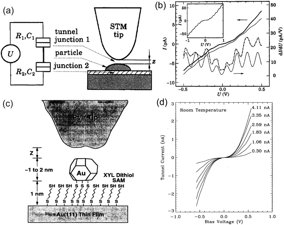 | ||
| Fig. 10 (a) Right: schematic image of the STM tip above an evaporated Au NP/ZrO2 (1 nm)/Au structure. The Au NP was physically adsorbed on the ZrO2 layer. Left: equivalent circuit of DBTJs. (b) Coulomb staircase at room temperature. Thick solid and dash-dotted curves represent I–V characteristics and the numerical differential conductance. Thin solid curves are obtained from theory and shifted vertically for clarity. Inset: Coulomb staircase at 4.2 K.71 Reprinted with permission from C. Schönenberger, H. Van Houten and H. C. Donkersloot, Single-Electron Tunnelling Observed at Room Temperature by Scanning-Tunnelling Microscopy. Eur. Phys. Lett., 1992, 3, 249–254. http://iopscience.iop.org/0295-5075/20/3/010. (c) Schematic image of an evaporated Au NP/dithiol SAM/Au(111) substrate. The Au NP was chemically anchored by the dithiol molecules. (d) Coulomb blockade at room temperature on a tethered 1.8 nm Au NP.73 Reprinted figures with permission from M. Dorogi, J. Gomez, R. Osifchin, R. P. Andres and R. Reifenberger, Phys. Rev. B: Condens. Matter Mater. Phys., 1995, 52, 9071–9077. Copyright 1995 by the American Physical Society. | ||
Next, organic SAMs were introduced as tunneling barriers. Initially, the tunneling barrier between the NPs and the substrate was the oxidized layer. Because the tunneling current strongly depends on the distance, the thickness of the insulating layer has to be atomically controlled. When a SAM acts as the tunneling barrier, we can control the thickness of the tunneling barrier by the length of the molecules. Alkanethiol molecules are the most famous SAMs, which consist of an alkyl chain with a thiol end group. Alkanethiol works as an insulator because all covalent chemical bonds are localized between the atoms (i.e., σ-bond). The length of an alkanethiol molecule increases by 0.13 nm with each addition of a carbon atom in the alkyl chain.163 Thus, an alkanethiol on the structure of the metal NP/alkanethiol/metallic surface is expected to help control the thickness of the tunneling barrier between the metals on the order of an angstrom.
In 1994, a room-temperature Coulomb staircase was demonstrated by STS for deposited Au NPs/alkanethiol/Au(111) film.72 The diameter and height of the Au NPs were 5–10 and 2–3 nm, respectively. The charging energy was estimated to be 180 meV by a rough capacitance evaluation using parallel-plate capacitor models. In later reports, double-ended thiol molecules (alkanedithiol) were also used as linkers between the deposited NPs and the Au(111) surfaces for the chemisorption of NPs. To realize more stable Coulomb staircases at room temperature, α,α′-xylyldithiol and 4,4′-biphenyldithiol SAMs were used to bind NPs deposited on an Au(111) surface by a cluster beam (Fig. 10(c) and (d)).73–75 A multiple expansion cluster source can generate Au NPs on the SAMs with diameters of ≈2 nm and heights of ≈1 nm. The resistance between a single Au NP and an Au(111) surface was estimated to be 18 ± 12 MΩ. This value corresponds to the calculated resistance of 4.5 ± 0.50 MΩ by the Landauer formula R′ = (h/2e2)T′.164 Deposited CdS,165,166 Co,167 and Pt NPs168,169 on SAMs were also studied. Recently, 0D levels of evaporated Au NPs on a 1,4-benzenedimethanethiol/Au(111) substrate were confirmed at 78 K.170
The coverage of Au deposited on octanethiol/Au(111) was investigated to determine the morphology of growing Au NPs.171 The self-capacitance of a single deposited Au NP on octanedithiol/Au(111) was strongly dependent on the surface coverage and its diameter.172–176 Sakotsubo et al. reported that the density of evaporated clusters can be controlled by using thiol–dithiol-mixed SAMs.176 Their results suggest that an isolated Au NP is appropriate for investigating the Coulomb blockade behavior at room temperature because the surrounding Au NPs display a parasitic capacitance and decrease the charging energy.
Synthesized NPs are generally passivated by organic molecules to avoid aggregating and sintering, i.e., they are initially covered by a tunneling barrier. The density of NPs deposited on a substrate can be controlled by changing the concentration of the NPs in solution, which is easier than controlling the density by evaporation methods. Because the NPs were isolated and size-controlled, synthesized NPs covered with ligand molecules were promising materials for Coulomb islands.
Initially, ligand-stabilized Pt NPs (comprising 309 Pt atoms) showed clear Coulomb staircases in STS measurements at 4.2 K.137,177 Several years later, the Coulomb staircases for a single synthesized Au NP with an atomic mass unit (amu) of 29 k were reported at up to room temperature.178,179 The Au NPs consisted of 147 ± 10 Au atoms in the core, corresponding to a diameter of 1.68 ± 0.04 nm, which was measured by mass spectrometry.179 The charging energy of the DBTJ was 75 meV, which was larger than the thermal fluctuations at room temperature (Fig. 11(a) and (b)).
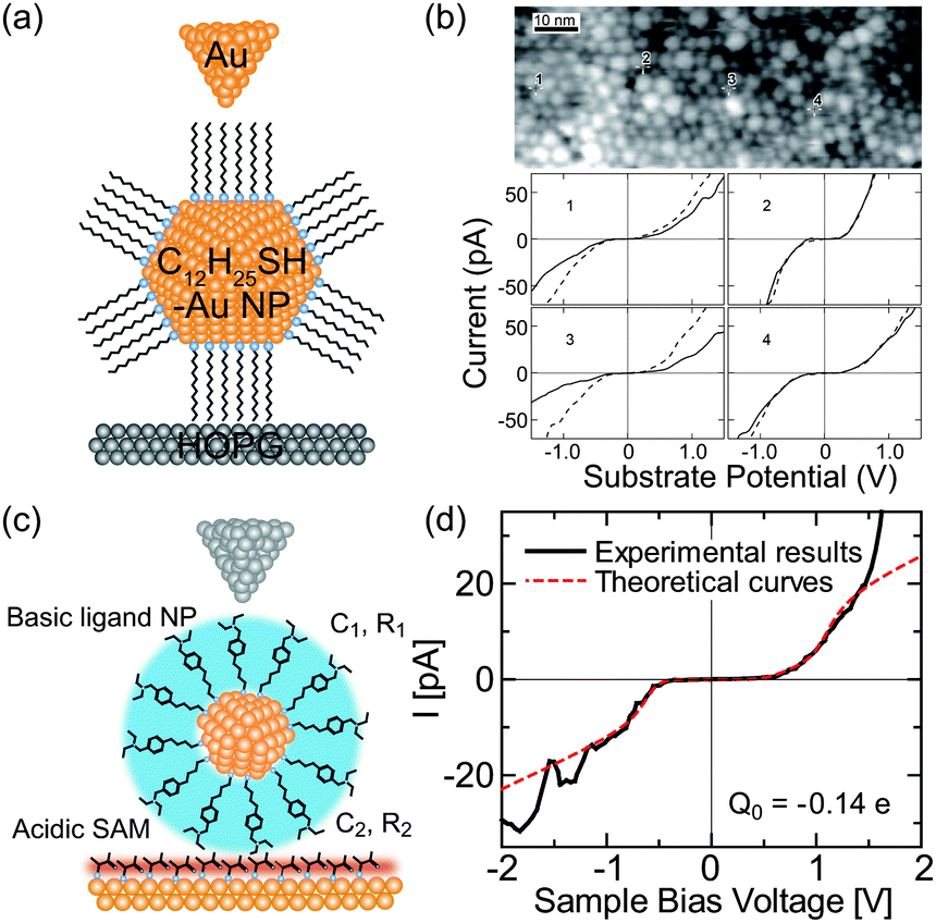 | ||
| Fig. 11 Room-temperature Coulomb blockade on synthesized nanoparticles. (a) Schematic image of DBTJs consisting of Au-tip/dodecanethiol-protected Au nanoparticle/HOPG structures. (b) Room temperature Coulomb blockade at several NPs in the STM images.179 Reprinted with permission from T. P. Bigioni, L. E. Harrell, W. G. Cullen, D. K. Guthrie, R. L. Whetten and P. N. First, Eur. Phys. J. D, 1999, 6, 355–364. Copyright 1999 Springer-Verlag. (c) Schematic image of DBTJs consisting of PtIr-tip/bis-4,40-(4,4′-dithiobutylbenzyl)-N,N,N′,N′-tetraethylamine (TBA) protected Au NP/Au(111) structures. (d) Room-temperature Coulomb blockade on TBA protected Au NP with a 1.8 nm diameter.84 Copyright (2011) The Japan Society of Applied Physics. | ||
Electrochemical cyclic voltammetry of Au-NPs solutions was used in an attempt to confirm the values of Ec by STS.41,178,180 Current peaks separated by e/Cdot were observed in the voltammograms, which were corresponding to the Coulomb staircases in the STS measurements. Cyclic voltammetry proved that Ec of Au NPs (1.64 nm diameters) exceeded ambient thermal fluctuation.178
Another novel observation in this report was that the 0D levels of the Au NPs affected the I–V characteristics. The observed dI/dV spectrum at 77 K included several peaks that could not be explained by the orthodox theory. These peaks indicated that the tunneling current increased because electrons were resonantly tunneling through the 0D levels.54 The calculated mean energy level spacing ΔE was estimated to be 45 meV, which also surpassed the thermal broadening at 77 K (3.5kBT = 23 meV).
Au NPs with various ligand molecules have been investigated by STM: alkanethiols,77,81–83,178,179,181,182 amino-type molecules,84,183 dendrimers,184 and polymers.185,186 The ligand molecules works as linkers between the NPs and the substrate by physical or chemical interactions. Octanethiol–octanedithiol-mixed ligands were used to anchor the 1.5 nm-diameter NPs to a bare Au(111) surface.181 The driving force in anchoring the NPs is attributed to the strong affinity of free thiols for Au atoms.187 The force of the Au–S covalent bond is ≈180 kJ mol−1, which is stronger than a hydrogen bond or van der Waals interaction. The stability of this bond can be attributed to the observation of a stable Coulomb blockade at room temperature using octanethiol–octanedithiol-mixed ligands.181
Au NPs surrounded by citric acids are negatively charged; thus, they selectively adsorb onto a positively charged surface functionalized by amino-substituted thiols.188,189 The Au NPs surrounded by amino-thiol can be anchored on a positively charged surface by carboxyl-substituted thiol as well.84 Room-temperature Coulomb blockades have been reported using positively charged 1.8 nm-diameter Au NPs chemisorbed on a thiolactic acid/Au(111) surface (Fig. 11(c) and (d)).84 Poly(propylene imine) dendrimers (guest) can be immobilized on SAMs of heptathioether-functionalized β-cyclodextrin (host) through host–guest interactions.184 The Au NPs protected by the dendrimer showed negative differential resistance peaks, attributed to the resonant tunneling of electrons through the molecular orbitals, in a room-temperature Coulomb staircase. Polyvinylpyrrolidone-protected Au NPs and Pd NPs on HOPG were used to control the charging energy of DBTJs.185 The charging energy of the NPs was inversely proportional to the diameter of the NPs, which corresponds to the classical expression for the capacitance of a metal sphere in a dielectric medium (4πεR, where ε is the dielectric constant of the medium and R is the diameter of the NPs).
In our previous studies, we investigated physisorbed and chemisorbed Au NPs on Au(111) surfaces at low temperature. Fig. 12 shows two STS results on physisorbed and chemisorbed octanethiol-protected Au NPs. More clear and predictable Coulomb staircases are observed in the chemisorbed Au NPs anchored by decanedithiol. This result indicates that the chemisorption of NPs can be attributed to the stable electrical characteristics of NPs.81,83
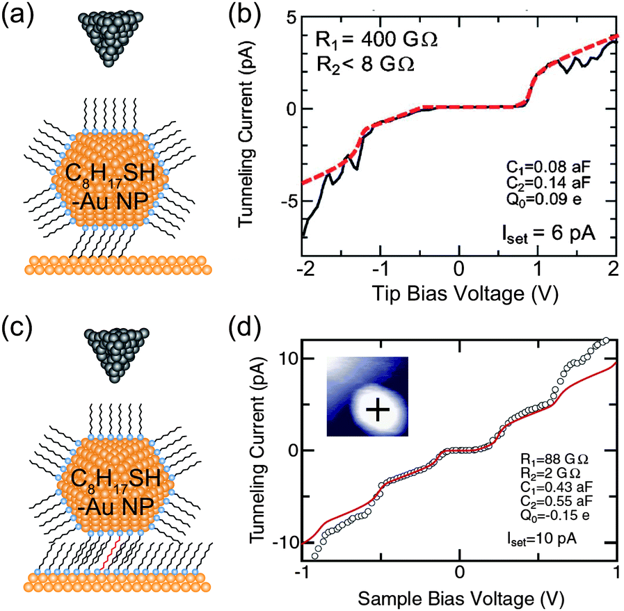 | ||
| Fig. 12 Effects of physisorption and chemisorption on Coulomb staircases. (a) Schematic image of DBTJs consisting of PtIr-tip/octanethiol-protected Au nanoparticle/Au(111) structures. The NP is physisorbed on the Au(111). (b) Experimental and theoretical Coulomb staircases at 68 K on the physisorbed 2.4 nm-Au NP (solid and dashed lines, respectively).81 Reprinted with permission from H. Zhang, Y. Yasutake, Y. Shichibu, T. Teranishi and Y. Majima, Phys. Rev. B: Condens. Matter Mater. Phys., 2005, 72, 205441. Copyright 2005 American Physical Society. (c) Schematic image of DBTJs consisting of PtIr-tip/octanethiol-protected Au nanoparticle/octanethiol, decanedithiol mixed SAMs/Au(111) structures. The NP is chemisorbed on the Au(111) via decanedithiol molecules. (d) Experimental and theoretical Coulomb staircases at 65 K on the chemisorbed 3.3 nm-Au NP (open circle and solid line, respectively).83 Copyright (2010) The Japan Society of Applied Physics. The theoretical curves of (b) and (d) were calculated by the orthodox theory. | ||
Electrical characteristics of various synthesized NPs have been reported in addition to Au NPs: Ag,85,190–193 Pt,137 Co,156,194 Pd,168,169,185 Au–Ag alloy,195 InAs,85,196–198 CdS,199 and CdSe.78,200–202 Tuning the bandgap of InAs NPs linked to an Au surface by hexanedithiol molecules has been demonstrated between 0.9 and 1.9 eV by changing the diameter of the NPs between 1.0 and 3.5 nm (Fig. 13(a)).196 The tunneling spectrum in the report indicated that an atomic-like Aufbau-principle filling of the s- and p-shells also occurred. The shell spectrum of CdSe and PbSe was quantitatively evaluated by low-temperature STS at 5 K (Fig. 13(b)).201,202 Single-electron tunneling through the 0D levels observed by STS provides significant information about the 0D spectrum of NPs.
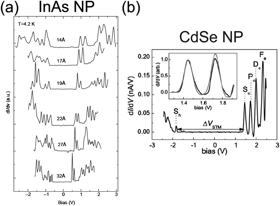 | ||
| Fig. 13 Observation of bandgap and 0D spectrum in semiconductor NPs by STS characterization. (a) Size evolution of dI/dV–V characteristics of single InAs NP at 4.2 K. The diameter of the NP ranges from 14 Å to 32 Å. The observed peaks are corresponding to resonant tunneling through the 0D energy levels of the NP.196 Reprinted with permission from U. Banin, Y. Cao, D. Katz and O. Millo, Nature, 1999, 400, 542–544. Copyright 1999 Macmillan Magazines Ltd. (b) dI/dV–V characteristics of single CdSe NP at 5 K. The diameter of the NP is 5 nm. The inset graph shows a good agreement of the experimental curves (black line) with theory (grey line).201 Reproduced from ref. 201 with permission from the PCCP Owner Societies. | ||
Reported single-electron effects of the synthesized NPs by STM are summarized in Table 2. The values of Ec are much larger than the thermal fluctuations at room temperature due to the small size of the NPs. It has been demonstrated that controlling the size of the synthesized NPs enables the control of Ec in SETs.62 Therefore, synthesized NPs are good candidates for single Coulomb islands in SETs.
| Elements | Ligands | Sorption | R (nm) | E c (meV) | T (K) | Ref. |
|---|---|---|---|---|---|---|
| RT: room temperature, N/A: not mentioned in the paper. | ||||||
| Pt | Phenanthroline and O2 | Physisorption | 1.68 ± 0.04 | 50 | 4.2 | 137 |
| Au | CH3(CH2)5SH | Physisorption | 1.1–1.9 | 75–164 | 83 | 41, 178 |
| Au | (Ph2PC6H4SO3H)12Cl6 | Electrostatic interaction | <2 | 57 | RT | 76 |
| Au | CH3(CH2)11SH | Physisorption | 1.7 | 75–167 | RT | 179 |
| Au or Ag | Galvinol, HS(CH2)6NH2, CH3(CH2)5SH | Physisorption | 2 | 30–148 | RT | 183 |
| Au | CH3(CH2)6SH | Physisorption | 15 ± 2.1 | 10 | 4.2 | 77 |
| 9.4 ± 1.5 | 19 | 4.2 | ||||
| 4.6 ± 1.2 | 39 | 4.2 | ||||
| 1.8 ± 0.6 | >200 | 4.2 | ||||
| Pt | Polyvinylpyrrolidone | Physisorption | 2.5 | 100 | RT | 185 |
| Au | Polyvinylpyrrolidone | Physisorption | 1.7 | 220 | RT | 185 |
| Ag | CH3(CH2)11SH | Physisorption | 3.5–7.7 | 300 | RT | 190 |
| Co | CH3(CH2)11COOH | Physisorption | 5.5 ± 1.0 | 250 | 77 | 194 |
| Ag | CH3(CH2)11SH | Physisorption | 4.3 ± 0.6 | 230–1000 | RT | 191 |
| Au | CH3(CH2)11SH | Physisorption | 7 ± 0.4 | 76 | 5 | 194 |
| Au | CH3(CH2)5SH | Physisorption | 2.1 ± 0.5 | 240–290 | 68 | 81 |
| CH3(CH2)7SH | Physisorption | 2.4 ± 0.5 | 140–360 | 68 | 81 | |
| Au | CH3(CH2)7SH and HS(CH2)8SH | Linked by HS(CH2)8SH | 1.5 | 450 | RT | 181 |
| Au | Poly(propyleneimine) dendrimer | Host–guest interaction | 1.7 ± 0.9 | 67 | RT | 184 |
| Au/Ag alloy | CH3(CH2)5SH and HS(CH2)8SH | Linked by HS(CH2)8SH | 1–2 | 200 | RT | 195 |
| Au | Triphenylphosphine | Linked by HS(CH2)10SH | <1 | 530 | 4.2 | 80 |
| Au | CH3(CH2)7SH | Linked by HS(CH2)10SH | 3.3 ± 0.5 | 82 | 65 | 83 |
| Au | Amino-type molecule | Electrostatic interaction | 1.8 ± 0.2 | 200–450 | RT | 84 |
| Au | Thiol-derivatized OPE | Linked by OPE derivative | 2.1 | 570 | 100 | 87 |
| InAs | Organic ligands | Linked by HS(CH2)6SH | 1–4 | 110 | 4.2 | 196 |
| CdS | N/A | Electrostatic interaction | 2.1 ± 0.3 | 90–160 | 300 | 165 |
| PbS | N/A | Electrostatic interaction | 3.2 ± 0.4 | 80–120 | 300 | 166 |
| CdSe | N/A | Physisorption | 4.3 ± 0.4 | 60 | 4.2 | 78 |
| CdSe | Hexylamine or pyridine | Linked by HS(CH2)6SH | 3–5 | >100 (0D spacing) | 5 | 97 |
| PbSe | Hexylamine or pyridine | Linked by HS(CH2)6SH | 4 | >100 (0D spacing) | 5 | 97 |
In this section, we described the history of the investigation of single-electron transport in single NPs by STM and STS. As the synthesis of NPs improved, several synthesized NPs have been characterized for applications in single-electron devices. Single-electron effects and electronic structures of a single NP can be revealed by STS measurements. The charging energy of a NP obtained by STS measurements is summarized in Table 2. STS is a powerful tool to explore candidates for Coulomb islands in single-electron transistors from the viewpoint of the charging energy.
4.2 Photon-emission from nanoparticles
Taking inelastic tunneling processes into consideration, it is expected that photons can be generated by inelastic electron tunneling between the STM tip and the substrate. Photon-emission in a single Ag NP has been explored with light-collection optics inside STM.108,191,193,203–206 Ag NPs exhibit a surface plasmon resonance at a wavelength of around 400 nm.203 The STM images and photon counts of an Ag NP were obtained simultaneously (Fig. 14(a)–(d)).108,193,205 By using the spectrum analysis of the emitted photon energies, the in-plane and out-of-plane plasmon modes were excited in the SAMs of Ag NPs.206 Photoluminescence switching was reproducibly observed in a single synthesized dodecanethiol-protected Ag NP on Au(111) at room temperature.204 Detailed analysis of the photon-emission spectrum enables the observation of single-NP luminescence in several images at the tenth-nm scale. This technique allows us to observe the local excited luminescence of a nanomaterial.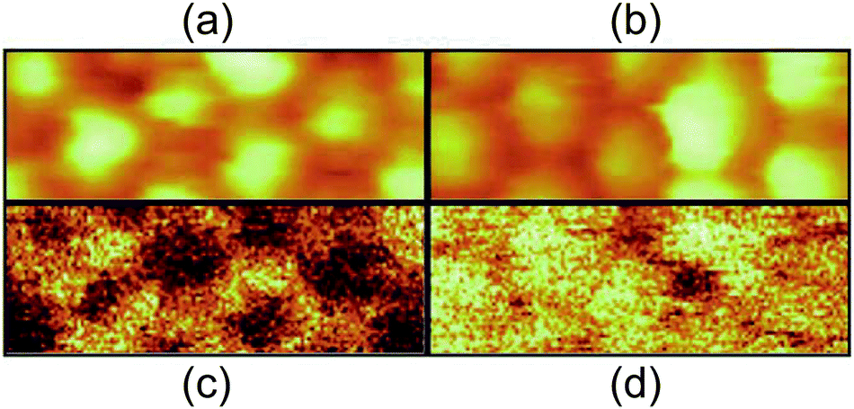 | ||
| Fig. 14 Simultaneously recorded STM topography ((a), (b)) and photon mapping ((c), (d)) of thiol-coated Ag NPs. The scan area is 26 × 10 nm2, sample bias voltage is 2.0 V in (a) and (c), 2.5 V in (b) and (d). The set-point current is 3.5 nA. White colour in the images represents a higher height and more photon emission.108 Reproduced from F. Silly, F. Charra, Luminescence induced using a scanning-tunneling microscope as a nanophotonic probe, 2002, 3, 493–500. Copyright 2002 Elsevier Masson SAS. All rights reserved. | ||
4.3 Molecular vibrational modes on nanoparticles
Vibrational modes of molecules on synthesized NPs are important issues when we consider photon-emission from the NPs. The effects of a ligand's vibration have been observed on photon-emission from tunneling barriers, confirmed by STM and other optical spectroscopies. It is well known that Raman signals originating from molecular vibration can be enhanced due to a strong electric field on metallic NPs (Surface-enhanced Raman scattering: SERS).207–210 Raman spectroscopy and STM experiments were carried out on a myristate-capped Ag NP and a 2-methyl-1-propanethiolate Ag NP onto dodecanethiol/Au substrates, which shows that the vibration of ligand molecules affects the photon emission from the samples (Fig. 15).211 High-resolution STM observation and Fourier transform infrared spectroscopy found the relationship between homogeneity of a mixed monolayer (1-octanethiol and its fully deuterated analogues) and CH2 stretching frequencies.212 Tunneling current through single NPs can be modulated by inelastic electron tunneling due to molecular vibration on the NPs;58 therefore, STS measurements are possible to detect the vibration of ligands and absorbed molecules on single NPs. In these two sections, we showed that STM and STS are useful tools in the fields of nanophotonics, the same as nanoelectronics.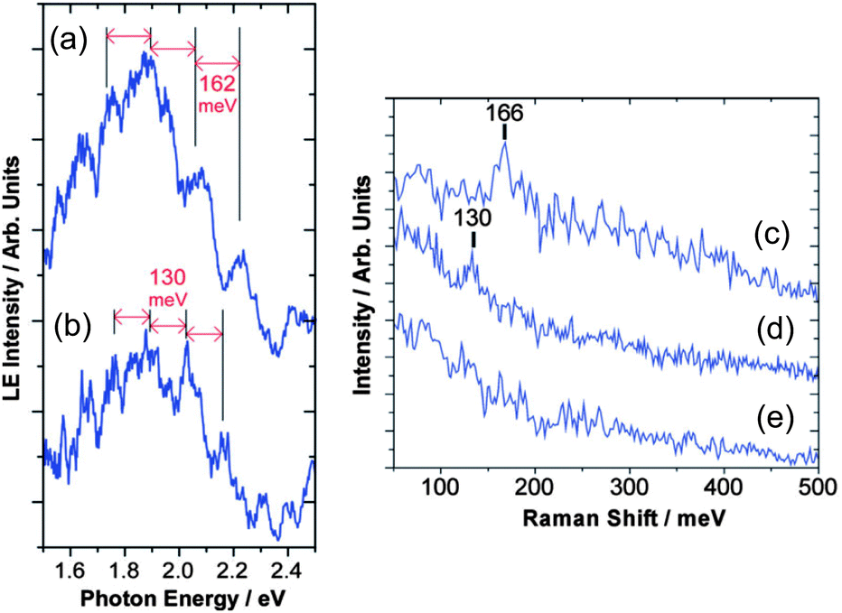 | ||
| Fig. 15 Light emission spectrum of (a) a myristate-capped Ag NP/dodecanethiol/Au substrate and (b) a 2-methyl-1-propanethiolate Ag NP/dodecanethiol/Au substrate with STM observation. The spectrum has periodical peaks superimposed on a broad spectrum. The Raman spectrum of (c) a myristate-capped Ag NP/dodecanethiol/Au substrate, (d) a 2-methyl-1-propanethiolate Ag NP/dodecanethiol/Au substrate and (e) a dodecanethiol/Au substrate are shown. The Raman shifts of the NPs in (c) and (d) are corresponding to the periods of the peaks in (a) and (b), respectively. Thus, the peaks can be attributed to the molecular vibration of the capping molecules on the NPs. Adapted from ref. 211 with permission from the PCCP Owner Societies. | ||
4.4 Surface morphology of molecules on nanoparticles
STM imaging techniques can obtain fruitful information regarding the ligand molecules on NPs. Structural understanding of NPs has been obtained by transmission electron microscopy and X-ray crystallography.213–215 Transmission electron microscopy is widely used to evaluate the size distribution and crystal structure of NPs. However, it is difficult to detect a thin ligand layer using the highly accelerated electron beam because most of the electrons penetrate the layer. X-ray diffraction gives information about a thin organic monolayer on a metal surface by the diffraction pattern. Conversely, STM can directly create an image of the ligand layer in real space, such as the morphology and electron density distribution. Low-temperature STM has been used to visualize the phenyl rings of ligand molecules at 7 K under UHV conditions, which was correlated with a model (Fig. 16(a) and (b)).39,216 High-resolution STM images of a mixed-ligand layer (e.g., octanethiol and mercaptopropionic acid) on Au and Ag NPs have also been reported.212,217–222 The observed images indicated that each ligand formed domains that were aligned to parallel ripples that spiraled around the NPs (Fig. 16(c) and (d)). The same group revealed that the mechanism for SAM formation on NPs is different from that on flat surfaces; the morphology is dependent on the diameter of NPs and the types of molecules.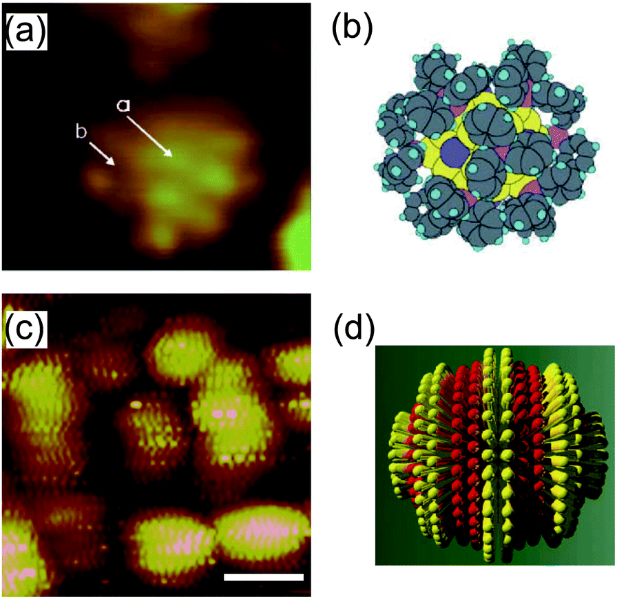 | ||
| Fig. 16 (a) STM image of an individual Au55 cluster protected by triphenylphosphine at 7 K. The light dots indicate phenyl rings of triphenylphosphine. (b) Schematic illustration of the Au55 cluster.216 Reprinted with permission from G. Schmid and B. Corain, Eur. J. Inorg. Chem., 2003, 3081–3098. Copyright 2003 Wiley-VCH. (c) STM image of octanethiol/mercaptopropionic acid mixed layer-protected Au NPs. The ligand shell shows phase separated ordered domains. Scale bar is 10 nm. (d) Schematic illustration of one single rippled NP. The yellow lobes represent octanethiols and the red lobes represent mercaptopropionic acids.217 Reprinted with permission from A. M. Jackson, J. W. Myerson and F. Stellacci, Nat. Mater., 2004, 3, 330–336. Copyright 2004 Nature Publishing Group. | ||
The height of the NPs in the STM images also affords morphological information about the ligand molecules. The lateral width of the STM images is broader than the true width of the objects because of tip convolution effects.223,224 In contrast, the height and distance between the NPs are not affected by the convolution of the STM tip and the objects.223 Therefore, it is more accurate to evaluate the diameter of NPs, including the ligands, from the height of the STM images. Ref. 49 showed that the height of the NPs in the image (2.2 nm) agreed well with the core diameter of the NPs (1.0 nm) and the height of the porphyrin molecules (0.6 nm), and hence proved the coordination pattern of thiol-derivatized porphyrins to Au NPs (e.g., six porphyrin faces surrounding each Au NP in a hexahedron).
By considering the set-point current dependence of a Coulomb staircase, the tunneling resistances of DBTJs can be estimated.81,84,87 Resistances of alkanethiols,81 a series of acid and base molecules,84 and OPE87 have been analyzed using the set-point current dependence. Zhang et al. estimated the resistance of hexanethiol and octanethiol on Au NPs as 460 MΩ and 7.6 GΩ, respectively (Fig. 17). It is noted that these tunneling resistances can be compared with those on reported solid-state single-electron transistors.62,63 STS is also a powerful tool to explore candidates for Coulomb islands in single-electron transistors from the viewpoint of the tunneling resistance.
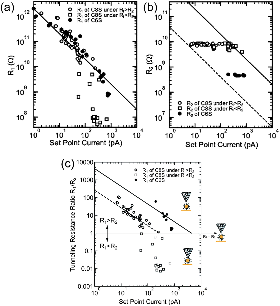 | ||
| Fig. 17 Set-point current dependence of (a) tunneling resistance R1, (b) tunneling resistance R2, and (c) tunneling resistance ratio R1/R2 under the structure STM-tip/hexanethiol (octanethiol)-protected Au NP/Au(111). Open circles represent octanethiol protected Au NP in the region of R1 > R2, open squares represent octanethiol-protected Au NP in the region of R1 > R2, and closed circles represent hexanethiol-protected Au NP.81 The dashed and solid lines show the relationship of the set-point current Iset and R1/R2, i.e., IsetR1/R2 = −260 pA (VsetR2 = −2 V/7.6 GΩ) and IsetR1/R2 = −4.3 nA (VsetR2 = −2 V/460 MΩ) for octanethiol and hexanethiol protected Au NPs, respectively. Reprinted with permission from H. Zhang, Y. Yasutake, Y. Shichibu, T. Teranishi and Y. Majima, Phys. Rev. B: Condens. Matter Mater. Phys., 2005, 72, 205441. Copyright 2005 American Physical Society. | ||
In this section, we showed that STM can provide information regarding the ligand molecules, such as the morphology, length, and tunneling resistance. Molecular-resolution STM reveals the geometrical order of ligand molecules on NPs. The length of ligand molecules can be estimated owing to the high sensitivity of the height information given by STM. The set-point current dependence of a Coulomb staircase provides the tunneling resistance of a ligand molecule on synthesized NPs.
4.5 Electrical-switching effects in single nanoparticles
Electrical-switching effects comprising functionalized NPs are interesting in possible applications of NPs.31,225,226 For example, a photoirradiation-induced switching of nanoparticle monolayers was attributed to the reversible photoisomerization of the diarylethene molecules bridging the NPs.225 A molecular floating-gate effect obtained by visible-light irradiation was observed in SETs with copper-phthalocyanine-doped Au NPs.68 In principle, the NP switching is due to the reversible properties of the ligands or linker molecules. STM has demonstrated many single-molecule switching effects in molecules such as OPE,227,228 endohedral metallofullerenes,8,15 and porphyrin and phthalocyanine derivatives.21,95,97,98 Therefore, it is possible to observe the switching phenomena of a single functionalized NP by STM.Blinking STM images of Au NPs tethered to thiol molecules have been reported.87,229 These blinking events, which were reversible and stochastic, were observed in alkanedithiol and OPE molecules inserted into alkanethiol SAMs.228,229 In this measurement, Au NPs were introduced to mark the blinking molecules. The blinking STM images were observed even after the attachment of Au NPs to the linker dithiol molecules; thus, the researchers concluded that the switching was caused by the thermally activated movement of the molecules tethered to the Au surface. The observed reversible switching was not attributed to breaking of the thiol–Au bond or a change in the free thiol group. There is also a report stating that the conductivity of Au NPs can be switched through redox effects of the linker molecule.86 Because the decay length of an electron changes from 16 nm−1 to 7 nm−1 during redox, the conductivity of the Au NPs through Au(111) changed greatly.
A single Au NP protected by OPE ligands also showed stochastic blinking events (Fig. 18(a) and (b)).87 The switching events had been observed several times during 80 min of continuous scanning. Decomposition or removal of the NPs was not observed because the relative position of the NPs in the images did not change. This result shows the possible functionalization of variously sized NPs by surrounding ligands. In this case, stochastic switching due to single-molecular properties can be observed at scales larger than the molecules.
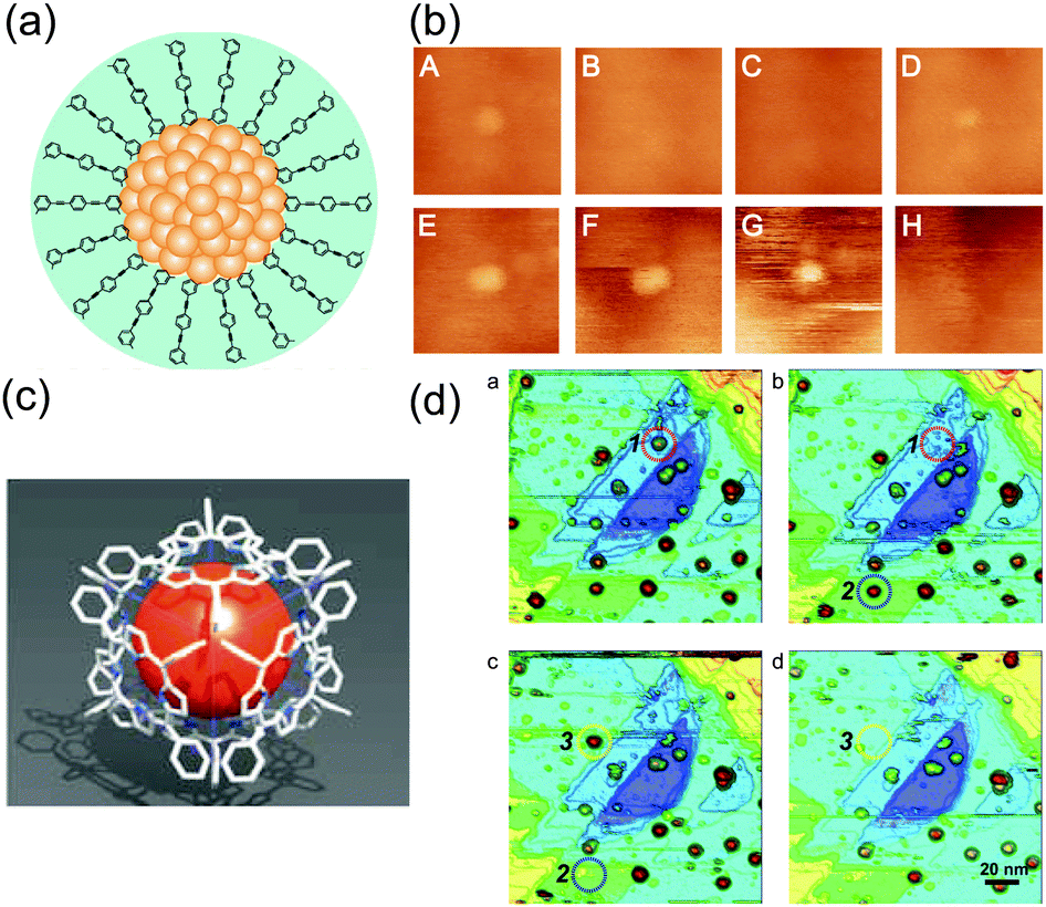 | ||
| Fig. 18 (a) Schematic illustration of Au NPs protected by thiol-derivatized OPE. (b) Stochastic switching phenomena of the Au NP in successive STM scanning for 80 min.87 The two solid lines are on the same Au NP and the height of the Au NP changes in the scans. Reprinted with permission from H. Koo, S. Kano, D. Tanaka, M. Sakamoto, T. Teranishi and Y. Majima, Appl. Phys. Lett., 2012 101, 083115. Copyright 2012 American Institute of Physics. (c) Schematic illustration of Au NPs protected by thiol-derivatized porphyrin molecules. (d) Erase manipulation of the Au NPs by the STM tip during successive STM scanning. Applying 3 V between the STM tip and the substrate makes the NPs disappear.49 Reprinted with permission from M. Sakamoto, D. Tanaka, H. Tsunoyama, T. Tsukuda, Y. Minagawa, Y. Majima and T. Teranishi, J. Am. Chem. Soc., 2012 134, 816–819. Copyright 2012 American Chemical Society. | ||
Sakamoto et al. demonstrated the erasure of Au NPs by STM at room temperature (Fig. 18(c) and (d)). The porphyrin-protected Au NPs were systematically removed by applying a voltage of 3.0 V to the Au NPs for 1 min. The quality of the STM images did not degrade even after erasing the NPs, which implies that the STM tip is kept clean during the erasing process. A possible mechanism for erasure may be the multistep reductive dissociation or heat decomposition of the NPs by inelastic tunneling currents. This erasure can be used as one-time write memory if we define the presence (absence) of NPs as 1 (0).
In this section, we summarized electrical-switching effects on NPs by using STM. The switching effects of NPs are attributed to the reversible physical properties of the surrounding molecules. Stochastic switching and one-time write switching have been reported as intriguing properties of single NPs. If we harness these switching phenomena, there appears a possibility for applying the solid-state memory device based on NPs.
5 Conclusions
STM and STS have become invaluable tools to characterize electrical and photonic properties of single synthesized NPs owing to the sub-nanometre scale topographies and measurements. Single electron effects of NPs, such as Coulomb blockades, have been demonstrated in detail, when combined with the theoretical calculation. The structural and electrical properties of ligand molecules on NPs have been also investigated. Photonic studies have been carried out on NPs by STM, which detects photons generated from molecular tunneling barriers. Stochastic blinking effects and one-write erasing behaviors of NPs are promising functions for the introduction of solid-state nanoscale memories based on synthesized NPs. Characterization methods for NPs by STM and STS reviewed here cover the significant interest for the NP functions towards the realization of solid-state nanodevices, especially for the diverse applications of single-electron transistors, nanoscale sensors or memories.Acknowledgements
The authors thank Prof. T. Teranishi, Kyoto Univ., for the syntheses of numerous NPs for our research collaborations. This study was partially supported by MEXT Elements Strategy Initiative to Form Core Research Center; by the Collaborative Research Project of Materials and Structures Laboratory, Tokyo Institute of Technology; by the Collaborative Research Program of the Institute for Chemical Research, Kyoto University (grant # 2014-73); and by the BK21 plus Program through the Ministry of Education, Science and Technology of Korea.References
- G. Binnig, H. Rohrer, Ch. Gerber and E. Weibel, Phys. Rev. Lett., 1982, 49, 61 CrossRef.
- J. Tersoff and D. R. Hamann, Phys. Rev. B: Condens. Matter Mater. Phys., 1985, 31, 2 CrossRef.
- G. Binnig and H. Rohrer, IBM J. Res. Dev., 1986, 30, 355 CAS.
- N. D. Lang, Phys. Rev. B: Condens. Matter Mater. Phys., 1986, 34, 5947 CrossRef.
- R. M. Feenstra, J. A. Stroscio and A. P. Fein, Surf. Sci., 1987, 181, 295 CrossRef CAS.
- G. Binnig, H. Rohrer, Ch. Gerber and E. Weibel, Phys. Rev. Lett., 1983, 50, 120 CrossRef CAS.
- M. Kuwabara, D. R. Clarke and D. A. Smith, Appl. Phys. Lett., 1990, 56, 2396–2398 CrossRef CAS.
- Y. Yasutake, Z. Shi, T. Okazaki, H. Shinohara and Y. Majima, Nano Lett., 2005, 5, 1057–1060 CrossRef CAS PubMed.
- P. A. Christensen, Chem. Soc. Rev., 1992, 21, 197–208 RSC.
- H. Rohrer, Surf. Sci., 1994, 299, 956 CrossRef.
- R. Wiesendanger, Scanning Probe Microscopy and Spectroscopy: Methods and Application, Cambridge University Press, Cambridge, 1994 Search PubMed.
- P. G. Collins, A. Zettl, H. Bando, A. Thess and R. E. Smalley, Science, 1997, 278, 100–103 CrossRef CAS.
- L. C. Venema, J. W. G. Wildöer, J. W. Janssen, S. J. Tans, H. L. J. Temminck Tuinstra, L. P. Kouwenhoven and C. Dekker, Science, 1999, 283, 52–55 CrossRef CAS PubMed.
- G. Li, A. Luican and E. Y. Andrei, Phys. Rev. Lett., 2009, 102, 176804 CrossRef PubMed.
- M. Iwamoto, D. Ogawa, Y. Yasutake, Y. Azuma, H. Umemoto, K. Ohashi, N. Izumi, H. Shinohara and Y. Majima, J. Phys. Chem. C, 2010, 114, 14704–14709 CAS.
- L. A. Bumm, J. J. Arnold, T. D. Dunbar, D. L. Allara and P. S. Weiss, J. Phys. Chem. B, 1999, 103, 8122 CrossRef CAS.
- R. E. Holmlin, R. Haag, M. L. Chabinyc, R. F. Ismagilov, A. E. Cohen, A. Terfort, M. A. Rampi and G. M. Whitesides, J. Am. Chem. Soc., 2001, 123, 5075–5085 CrossRef CAS PubMed.
- W. Wang, T. Lee and M. A. Reed, Phys. Rev. B: Condens. Matter Mater. Phys., 2003, 68, 035416 CrossRef.
- X. Xiao, L. A. Nagahara, A. M. Rawlett and N. Tao, J. Am. Chem. Soc., 2005, 127, 9235–9240 CrossRef CAS PubMed.
- N. J. Tao, Nat. Nanotechnol., 2006, 1, 173–181 CrossRef CAS PubMed.
- S. Kano, Y. Yamada, K. Tanaka and Y. Majima, Appl. Phys. Lett., 2012, 100, 053101 CrossRef.
- Y. Majima, D. Ogawa, M. Iwamoto, Y. Azuma, E. Tsurumaki and A. Osuka, J. Am. Chem. Soc., 2013, 135, 14159–14166 CrossRef CAS PubMed.
- W. P. Halperin, Rev. Mod. Phys., 1986, 58, 533–606 CrossRef CAS.
- A. P. Alivisatos, Science, 1996, 271, 933–937 CAS.
- C. N. R. Rao, G. U. Kulkarni, P. J. Thomas and P. P. Edwards, Chem. Soc. Rev., 2000, 29, 27–35 RSC.
- T. Teranishi, C. R. Chim., 2003, 6, 979–987 CrossRef CAS.
- M.-C. Daniel and D. Astruc, Chem. Rev., 2004, 104, 293–346 CrossRef CAS PubMed.
- I. L. Medintz, H. T. Uyeda, E. R. Goldman and H. Mattoussi, Nat. Mater., 2005, 4, 435–446 CrossRef CAS PubMed.
- A. Z. Khosousi and A.-A. Dhirani, Chem. Rev., 2008, 108, 4072–4124 CrossRef PubMed.
- D. V. Talapin, J.-S. Lee, M. V. Kovalenko and E. V. Shevchenko, Chem. Rev., 2010, 110, 389–458 CrossRef CAS PubMed.
- R. Klajn, J. F. Stoddart and B. A. Grzybowski, Chem. Soc. Rev., 2010, 39, 2203–2237 RSC.
- M. Homberger and U. Simon, Philos. Trans. R. Soc., A, 2010, 368, 1405–1453 CrossRef CAS PubMed.
- A. Verma and F. Stellacci, Small, 2010, 6, 12–21 CrossRef CAS PubMed.
- F. A. Zwanenburg, A. S. Dzurak, A. Morello, M. Y. Simmons, L. C. L. Hollenberg, G. Klimeck, S. Rogge, S. N. Coppersmith and M. A. Eriksson, Rev. Mod. Phys., 2013, 85, 961–1019 CrossRef CAS.
- X. Cheng, S. B. Lowe, P. J. Reece and J. J. Gooding, Chem. Soc. Rev., 2014, 43, 2680–2700 RSC.
- A. Comin and L. Manna, Chem. Soc. Rev., 2014, 43, 3957–3975 RSC.
- S. M. Reimann and M. Manninen, Rev. Mod. Phys., 2002, 74, 1283–1342 CrossRef CAS.
- W. G. van der Wiel, S. De Franceschi, J. M. Elzerman, T. Fujisawa, S. Tarucha and L. P. Kouwenhoven, Rev. Mod. Phys., 2003, 75, 1–22 CrossRef CAS.
- G. Schmid, Chem. Rev., 1992, 92, 1709–1727 CrossRef CAS.
- M. Brust, M. Walker, D. Bethell, D. J. Schiffrin and R. Whyman, J. Chem. Soc., Chem. Commun., 1994, 801 RSC.
- S. Chen, R. S. Ingram, M. J. Hostetler, J. J. Pietron, R. W. Murray, T. G. Schaaff, J. T. Khoury, M. M. Alvarez and R. L. Whetten, Science, 1998, 280, 2098–2101 CrossRef CAS PubMed.
- S. Chen, J. Phys. Chem. B, 2000, 104, 663–667 CrossRef CAS.
- M. Brust and C. J. Kiely, Colloids Surf., A, 2002, 202, 175–186 CrossRef CAS.
- G. H. Woehrle, M. G. Warner and J. E. Hutchison, J. Phys. Chem. B, 2002, 106, 9979–9981 CrossRef CAS.
- T. Teranishi, S. Hasegawa, T. Shimizu and M. Miyake, Adv. Mater., 2001, 13, 1699–1701 CrossRef CAS.
- M. Kanehara, Y. Oumi, T. Sano and T. Teranishi, J. Am. Chem. Soc., 2003, 125, 8708–8709 CrossRef CAS PubMed.
- Y. Shichibu, Y. Negishi, T. Tsukuda and T. Teranishi, J. Am. Chem. Soc., 2005, 127, 13464–13465 CrossRef CAS PubMed.
- E. S. Shibu, M. A. Habeeb Muhammed, T. Tsukuda and T. Pradeep, J. Am. Chem. Soc., 2008, 112, 12168–12176 CAS.
- M. Sakamoto, D. Tanaka, H. Tsunoyama, T. Tsukuda, Y. Minagawa, Y. Majima and T. Teranishi, J. Am. Chem. Soc., 2012, 134, 816–819 CrossRef CAS PubMed.
- M. Sakamoto, D. Tanaka and T. Teranishi, Chem. Sci., 2013, 4, 824 RSC.
- M. L. Mastronardi, F. M. Flaig, D. Faulkner, E. J. Henderson, C. Kü bel, U. Lemmer and G. A. Ozin, Nano Lett., 2012, 12, 337–342 CrossRef CAS PubMed.
- H. Sugimoto, M. Fujii, K. Imakita, S. Hayashi and K. Akamatsu, J. Phys. Chem. C, 2013, 117, 11850–11857 CAS.
- F. Kuemmeth, K. I. Bolotin, S.-F. Shi and D. C. Ralph, Nano Lett., 2008, 8, 4506–4512 CrossRef CAS PubMed.
- S. Kano, Y. Azuma, K. Maeda, D. Tanaka, M. Sakamoto, T. Teranishi, L. W. Smith, C. G. Smith and Y. Majima, ACS Nano, 2012, 6, 9972 CrossRef CAS PubMed.
- L. M. Wheeler, N. R. Neale, T. Chen and U. R. Kortshagen, Nat. Commun., 2013, 4, 2197 Search PubMed.
- D. L. Klein, R. Roth, A. K. L. Lim, A. P. Alivisatos and P. L. McEuen, Nature, 1997, 389, 699–701 CrossRef CAS.
- T. Sato, H. Ahmed, D. Brown and B. F. G. Johnson, J. Appl. Phys., 1997, 82, 696–701 CrossRef CAS.
- K. Luo, D.-H. Chae and Z. Yao, Nanotechnology, 2007, 18, 465203 CrossRef PubMed.
- V. Ray, R. Subramanian, P. Bhadrachalam, L.-C. Ma, C.-U. Kim and S. J. Koh, Nat. Nanotechnol., 2008, 3, 603–608 CrossRef CAS PubMed.
- Y. Azuma, Y. Yasutake, K. Kono, M. Kanehara, T. Teranishi and Y. Majima, Jpn. J. Appl. Phys., 2010, 49, 090206 CrossRef.
- Y. Azuma, S. Suzuki, K. Maeda, N. Okabayashi, D. Tanaka, M. Sakamoto, T. Teranishi, M. R. Buitelaar, C. G. Smith and Y. Majima, Appl. Phys. Lett., 2011, 99, 073109 CrossRef.
- N. Okabayashi, K. Maeda, T. Muraki, D. Tanaka, M. Sakamoto, T. Teranishi and Y. Majima, Appl. Phys. Lett., 2012, 100, 033101 CrossRef.
- K. Maeda, N. Okabayashi, S. Kano, S. Takeshita, D. Tanaka, M. Sakamoto, T. Teranishi and Y. Majima, ACS Nano, 2012, 6, 2798 CrossRef CAS PubMed.
- G. Hackenberger, S. Kano, Y. Azuma, S. Takeshita, D. Tanaka, M. Sakamoto, T. Teranishi, Y. Ohno, K. Maehashi, K. Matsumoto and Y. Majima, Jpn. J. Appl. Phys., 2013, 52, 110101 CrossRef.
- S. Kano, Y. Azuma, D. Tanaka, M. Sakamoto, T. Teranishi, L. W. Smith, C. G. Smith and Y. Majima, J. Appl. Phys., 2013, 114, 223717 CrossRef.
- Y. Noguchi, T. Terui, T. Katayama, M. M. Matsushita and T. Sugawara, J. Appl. Phys., 2010, 108, 094313 CrossRef.
- M. Yamamoto, T. Terui, R. Ueda, K. Imazu, K. Tamada, T. Sakano, K. Matsuda, H. Ishii and Y. Noguchi, Appl. Phys. Lett., 2012, 101, 023103 CrossRef.
- Y. Noguchi, M. Yamamoto, H. Ishii, R. Ueda, T. Terui, K. Imazu, K. Tamada, T. Sakano and K. Matsuda, Jpn. J. Appl. Phys., 2013, 52, 110102 CrossRef.
- J. Liao, L. Bernard, M. Langer, C. Schönenberger and M. Calame, Adv. Mater., 2006, 18, 2444–2447 CrossRef CAS.
- Q. Sun, Y. A. Wang, L. S. Li, D. Y. Wang, T. Zhu, J. Xu, C. H. Yang and Y. F. Li, Nat. Photonics, 2007, 1, 717–722 CrossRef CAS.
- C. Schönenberger, H. V. Houten and H. C. Donkersloot, Europhys. Lett., 1992, 20, 249 CrossRef.
- D. Anselmetti, T. Richmond, A. Baratoff, G. Borer, M. Dreier, M. Bernasconi and H.-J. Güntherodt, Europhys. Lett., 1994, 25, 297–302 CrossRef CAS.
- M. Dorogi, J. Gomez, R. Osifchin, R. P. Andres and R. Reifenberger, Phys. Rev. B: Condens. Matter Mater. Phys., 1995, 52, 9071–9077 CrossRef CAS.
- R. P. Andres, T. Bein, M. Dorogi, S. Feng, J. I. Henderson, C. P. Kubiak, W. Mahoney, R. Osifchin and R. Reifenberger, Science, 1996, 272, 1323–1325 CAS.
- R. P. Andres, S. Datta, M. Dorogi, J. Gomez, J. I. Henderson, D. B. Janes, V. R. Kolagunta, C. P. Kubiak, W. Mahoney, R. F. Osifchin, R. Reifenberger, M. P. Smanta and W. Tian, J. Vac. Sci. Technol., A, 1996, 14, 1178–1183 CAS.
- L. F. Chi, M. Hartig, T. Drechsler, Th. Schwaach, C. Seidel, H. Fuchs and G. Schmid, Appl. Phys. A: Mater. Sci. Process., 1998, 66, S187–S190 CrossRef CAS.
- B. Wang, H. Wang, H. Li, C. Zeng, J. G. Hou and X. Xiao, Phys. Rev. B: Condens. Matter Mater. Phys., 2000, 63, 035403 CrossRef.
- E. P. A. M. Bakkers, Z. Hens, A. Zunger, A. Franceschetti, L. P. Kouwenhoven, L. Gurevich and D. Vanmaekelbergh, Nano Lett., 2001, 1, 551–556 CrossRef CAS.
- T. Baron, P. Gentile, N. Magnea and P. Mur, Appl. Phys. Lett., 2001, 79, 1175–1177 CrossRef CAS.
- R. K. Smith, S. U. Nanayakkara, G. H. Woehrle, T. P. Pearl, M. M. Blake, J. E. Hutchison and P. S. Weiss, J. Am. Chem. Soc., 2006, 128, 9266–9267 CrossRef CAS PubMed.
- H. Zhang, Y. Yasutake, Y. Shichibu, T. Teranishi and Y. Majima, Phys. Rev. B: Condens. Matter Mater. Phys., 2005, 72, 205441 CrossRef.
- Y. Majima, Y. Azuma and K. Nagano, Appl. Phys. Lett., 2005, 87, 163110 CrossRef.
- X. Li, Y. Yasutake, K. Kono, M. Kanehara, T. Teranishi and Y. Majima, Jpn. J. Appl. Phys., 2009, 48, 04C180 Search PubMed.
- S. Kano, Y. Azuma, M. Kanehara, T. Teranishi and Y. Majima, Appl. Phys. Express, 2010, 3, 105003 CrossRef.
- D. Mocatta, G. Cohen, J. Schattner, O. Millo, E. Rabani and U. Banin, Science, 2011, 332, 77 CrossRef CAS PubMed.
- D. I. Gittins, D. Bethell, D. J. Schiffrin and R. J. Nichols, Nature, 2000, 408, 67–69 CrossRef CAS PubMed.
- H. Koo, S. Kano, D. Tanaka, M. Sakamoto, T. Teranishi and Y. Majima, Appl. Phys. Lett., 2012, 101, 083115 CrossRef.
- C. Vericat, M. E. Vela, G. Benitez, P. Carro and R. C. Salvarezza, Chem. Soc. Rev., 2010, 39, 1805–1834 RSC.
- N. Camillone, C. E. D. Chidsey, G.-y. Liu and G. Scoles, J. Chem. Phys., 1993, 98, 3503 CrossRef CAS.
- G. E. Poirier and M. J. Tarlov, Langmuir, 1994, 10, 2853 CrossRef CAS.
- G. E. Poirier and E. D. Pylant, Science, 1996, 272, 1145–1148 CAS.
- When a bias voltage is applied between the STM tip and the metal electrode, it is considered that electric field is applied to the alkanethiol monolayer. So in a strict sense, the electric potential of the alkanethiol monolayer is different from that of the metal electrode. Even if coherent conduction is assumed, the single electron transmission probability is not as simple as eqn (1). Moreover, electron transport through nano-scale systems, such as molecular systems, is a highly non-equilibrium statistical problem. A theoretical model on this subject has not yet been established up to the present. In the case of incoherent conduction through molecular systems in particular, more sophisticated theoretical models are required in the future. However, discussion on this subject is beyond our review paper.
- J. G. Simmons, J. Appl. Phys., 1963, 34, 1793–1803 CrossRef.
- M. F. Crommie, C. P. Lutz and D. M. Eigler, Science, 1993, 262, 218–220 CAS.
- F. Moresco, G. Meyer, K.-H. Rieder, H. Tang, A. Gourdon and C. Joachim, Phys. Rev. Lett., 2001, 86, 672 CrossRef CAS PubMed.
- J. Repp, G. Meyer, F. E. Olsson and M. Persson, Science, 2004, 305, 493–495 CrossRef CAS PubMed.
- P. Liljeroth, J. Repp and G. Meyer, Science, 2007, 317, 1203–1206 CrossRef CAS PubMed.
- S. W. Wu, N. Ogawa, G. V. Nazin and W. Ho, J. Phys. Chem. C, 2008, 112, 5141–5244 Search PubMed.
- B. Xu and N. J. Tao, Science, 2003, 301, 1221–1223 CrossRef CAS PubMed.
- B. Xu, P. Zhang and N. Tao, Nano Lett., 2004, 4, 1105–1108 CrossRef CAS.
- M. Kiguchi, S. Miura, K. Hara, M. Sawamura and K. Murakoshi, Appl. Phys. Lett., 2006, 89, 213104 CrossRef.
- R. J. Hamers, R. M. Tromp and J. E. Demuth, Phys. Rev. Lett., 1986, 56, 1972–1975 CrossRef CAS PubMed.
- B. C. Stipe, M. A. Rezaei and W. Ho, Science, 1998, 280, 1732–1735 CrossRef CAS PubMed.
- A. J. Heinrich, C. P. Lutz, J. A. Gupta and D. M. Eigler, Science, 2002, 298, 1381–1387 CrossRef CAS PubMed.
- N. Okabayashi, Y. Konda and T. Komeda, Phys. Rev. Lett., 2008, 100, 217801 CrossRef PubMed.
- J. K. Gimzewski, J. K. Sass, R. R> Schlitter and J. Schott, Europhys. Lett., 1989, 8, 435–440 CrossRef.
- M. M. J. Bischoff, M. C. M. M. van der Wielen and H. van Kempen, Surf. Sci., 1998, 400, 127–133 CrossRef CAS.
- F. Silly and F. Charra, C. R. Phys., 2002, 3, 493–500 CrossRef CAS.
- H. Song, Y. Kim, Y. H. Jang, H. Jeong, M. A. Reed and T. Lee, Nature, 2009, 462, 1039–1043 CrossRef CAS PubMed.
- A. Mangin, A. Anthore, M. L. Della Rocca, E. Boulat and P. Lafarge, Phys. Rev. B: Condens. Matter Mater. Phys., 2009, 80, 235432 CrossRef.
- Y. Naitoh, S. Takeshita, D. Ishida, E. Ohmura, K. Kobayashi, H. Yamada and Y. Majima, Appl. Phys. Express, 2012, 5, 085201 CrossRef.
- K. K. Likharev, Proc. IEEE, 1999, 87, 606 CrossRef CAS.
- Z. A. K. Durrani, Single-Electron Devices and Circuits in Silicon; Imperial College, London, 2009, ch. 2 Search PubMed.
- A. E. Hanna and M. Tinkham, Phys. Rev. B: Condens. Matter Mater. Phys., 1991, 44, 5919–5922 CrossRef.
- M. A. Kastner, Rev. Mod. Phys., 1992, 64, 849–858 CrossRef.
- K. Yano, T. Ishii, T. Hashimoto, T. Kobayashi, F. Murai and K. Seki, IEEE Trans. Electron Devices, 1994, 41, 1628–1638 CrossRef.
- J. P. Pekola, O.-P. Saira, V. F. Maisi, A. Kemppinen, M. Mött
![[n with combining umlaut]](https://www.rsc.org/images/entities/char_006e_0308.gif) en, Y. A. Pashkin and D. V. Averin, Rev. Mod. Phys., 2013, 85, 1421–1472 CrossRef.
en, Y. A. Pashkin and D. V. Averin, Rev. Mod. Phys., 2013, 85, 1421–1472 CrossRef. - L. Zhuang, L. Guo and S. Y. Chou, Appl. Phys. Lett., 1998, 72, 1205 CrossRef CAS.
- B. H. Choi, S. W. Hwang, L. G. Kim, H. C. Shin, Y. Kim and E. K. Kim, Appl. Phys. Lett., 1998, 73, 3129 CrossRef CAS.
- S. J. Shin, C. S. Jung, B. J. Park, T. K. Yoon, J. J. Lee, S. J. Kim, J. B. Choi, Y. Takahashi and D. G. Hasko, Appl. Phys. Lett., 2010, 97, 103101 CrossRef.
- S. Lee, Y. Lee, E. B. Song and T. Hiramoto, Nano Lett., 2014, 14, 71–77 CrossRef CAS PubMed.
- H. W. Ch. Postma, T. Teepen, Z. Yao, M. Grifoni and C. Dekker, Science, 2001, 293, 76–79 CrossRef PubMed.
- M. Maeda, S. Iwasaki, T. Kamimura, K. Murata and K. Matsumoto, Jpn. J. Appl. Phys., 2008, 47, 5724 CrossRef CAS.
- Y. Oyama, Y. Majima and M. Iwamoto, J. Appl. Phys., 1999, 86, 7087 CrossRef CAS.
- Y. Azuma, M. Kanehara, T. Teranishi and Y. Majima, Phys. Rev. Lett., 2006, 96, 016108 CrossRef PubMed.
- N. W. Ashcroft and N. D. Mermin, Solid State Physics, Saunder College Publishing, Philadelphia, PA, 1976 Search PubMed.
- M. Fujii, O. Mamezaki, S. Hayashi and K. Yamamoto, J. Appl. Phys., 1998, 83, 1507–1512 CrossRef CAS.
- Z. A. K. Durrani and M. A. Rafiq, Microelectron. Eng., 2009, 86, 456–466 CrossRef CAS.
- D. V. Averin, A. N. Korotkov and K. K. Likharev, Phys. Rev. B: Condens. Matter Mater. Phys., 1991, 44, 6199 CrossRef.
- C. W. J. Beenakker, Phys. Rev. B: Condens. Matter Mater. Phys., 1991, 44, 1646–1656 CrossRef.
- M. Pierre, R. Wacquez, X. Jehl, M. Ssanquer, M. Vinet and O. Cueto, Nat. Nanotechnol., 2009, 5, 133–137 CrossRef PubMed.
- M. Fuechsle, S. Mahapatra, F. A. Zwanenburg, M. Friesen, M. A. Eriksson and M. Y. Simmons, Nat. Nanotechnol., 2010, 5, 502–506 CrossRef CAS PubMed.
- M. Fuechsle, J. A. Miwa, S. Mahapatra, H. Ryu, S. Lee, O. Warschkow, L. C. L. Hollenberg, G. Klimech and M. Y. Simmons, Nat. Nanotechnol., 2012, 7, 242–246 CrossRef CAS PubMed.
- S. Chen and R. W. Murray, Langmuir, 1999, 15, 682–689 CrossRef CAS.
- S. Chen, Langmuir, 1999, 15, 7551–7557 CrossRef CAS.
- F. Deng, Y. Yang, S. Hwang, Y.-S. Shon and S. Chen, Anal. Chem., 2004, 76, 6102–6107 CrossRef CAS PubMed.
- J. G. A. Dubois, J. W. Gerritssen, S. E. Shafranjuk, E. J. G. Boon, G. Schmid and H. van Kempen, Europhys. Lett., 1996, 33, 279–284 CrossRef CAS.
- H. Kitazawa, K. Albrecht and K. Yamamoto, Chem. Lett., 2012, 41, 828–830 CrossRef CAS.
- C. B. Murray, D. J. Norris and M. G. Bawendi, J. Am. Chem. Soc., 1993, 115, 8706–8715 CrossRef CAS.
- C. B. Murray, C. R. Kagan and M. G. Bawendi, Science, 1995, 270, 1335–1338 CAS.
- A. A. Guzelian, U. Banin, A. V. Kadavanich, X. Peng and A. P. Alivisatos, Appl. Phys. Lett., 1996, 69, 1432 CrossRef CAS.
- O. I. Micic, J. R. Sprague, C. J. Curtis, K. M. Jones, J. L. Machol, A. J. Nozik, H. Giessen, B. Fluegel, G. Mohs and N. Peyghambarian, J. Phys. Chem., 1995, 99, 7754–7759 CrossRef CAS.
- T. Teranishi and M. Miyake, Chem. Mater., 1998, 10, 594–600 CrossRef CAS.
- N. Zheng, J. Fan and G. D. Stucky, J. Am. Chem. Soc., 2006, 128, 6550–6551 CrossRef CAS PubMed.
- D. J. Fuchs and P. S. Weiss, Nanotechnology, 2010, 18, 044021 CrossRef.
- S. Hattori, S. Kano, Y. Azuma and Y. Majima, J. Phys. Chem. C, 2010, 114, 8120–8125 CAS.
- S. Hattori, S. Kano, Y. Azuma, D. Tanaka, M. Sakamoto, T. Teranishi and Y. Majima, Nanotechnology, 2012, 23, 185704 CrossRef PubMed.
- L. Kasprzak, R. Laibowitz, S. Head and M. Ohring, Thin Solid Films, 1974, 22, 189–196 CrossRef CAS.
- I. Giaever and H. R. Zeller, Phys. Rev. Lett., 1968, 20, 1504 CrossRef CAS.
- J. Lambe and R. C. Jaklevic, Phys. Rev. Lett., 1969, 22, 1371–1375 CrossRef.
- J. B. Barner and S. T. Ruggiero, Phys. Rev. Lett., 1987, 57, 807–810 CrossRef.
- P. J. M. van Bentum, R. T. M. Smokers and H. van Kempen, Phys. Rev. Lett., 1988, 60, 2543–2546 CrossRef PubMed.
- H. van Kempen, P. J. M. van Bentum and R. T. M. Smokers, Phys. Scr., T, 1992, 42, 153–158 CrossRef.
- E. Bar-Sadeh, Y. Goldstein, C. Zhang, H. Deng, B. Abeles and O. Millo, Phys. Rev. B: Condens. Matter Mater. Phys., 1994, 50, 8961–8964 CrossRef CAS.
- L. Wang, M. E. Taylor and M. E. Welland, Surf. Sci., 1995, 322, 325–336 CrossRef CAS.
- K. Schouteden, A. Lando, E. Janssens, C. V. Haesendonck and P. Lievens, New J. Phys., 2008, 10, 083005 CrossRef.
- R. Wilkins, E. Ben-Jacob and R. C. Jaklevic, Phys. Rev. Lett., 1989, 63, 801–804 CrossRef CAS PubMed.
- M. Amman, R. Wilkins, E. Ben-Jacob, P. D. Maker and R. C. Jaklevic, Phys. Rev. B: Condens. Matter Mater. Phys., 1991, 43, 1146–1149 CrossRef.
- J.-C. Wan, K. A. McGreer, N. Anand, E. Nowak and A. M. Goldman, Phys. Rev. B: Condens. Matter Mater. Phys., 1990, 42, 5604–5609 CrossRef CAS.
- A. Bettac, L. Köller, V. Rank and K. H. Meiwes-Broer, Surf. Sci., 1998, 402–404, 475–479 CrossRef CAS.
- H. N. Aier, V. Vijayakrishnan, G. N. Subbanna and C. N. R. Rao, Surf. Sci., 1994, 313, 392–398 CrossRef.
- C. P. Vinod, G. U. Kulkarni and C. N. R. Rao, Chem. Phys. Lett., 1998, 289, 329–333 CrossRef CAS.
- N. Camillone III, T. Y. B. Leung, P. Schwartz, P. Eisenberger and G. Scoles, Langmuir, 1996, 12, 2737 CrossRef.
- M. P. Samanta, W. Tian, S. Datta, J. I. Henderson and C. P. Kubiak, Phys. Rev. B: Condens. Matter Mater. Phys., 1996, 53, 7626 CrossRef.
- P. Jiang, Z. F. Liu and S. M. Cai, Appl. Phys. Lett., 1999, 75, 3023–3025 CrossRef CAS.
- P. Jiang, Z. F. Liu and S. M. Cai, J. Appl. Phys., 2001, 90, 2039–2041 CrossRef CAS.
- R. Breitwieser, P. Campiglio, C. Chacon, V. Repain, R. Nemausat, Y. Girard, J. Lagoute and S. Rousset, Surf. Sci., 2012, 606, 542–548 CrossRef CAS.
- N. Oncel, A.-S. Hallback, H. J. W. Zandvliet, E. A. Speets, B. J. Ravoo, D. N. Reinhoudt and B. Poelsema, J. Chem. Phys., 2005, 123, 044703 CrossRef PubMed.
- E. A. Speets, B. Dordi, B. J. Ravoo, N. Oncel, A.-S. Hallbäck, H. J. W. Zandvliet, B. Poelsema, G. Rijnders, D. H. A. Blank and D. N. Reinhoudt, Small, 2005, 1, 395–398 CrossRef CAS PubMed.
- K. Schouteden, N. Vandamme, E. Janssen, P. Lievens and C. V. Haesendonck, Surf. Sci., 2008, 602, 552–558 CrossRef CAS.
- T. Ohgi, H.-Y. Sheng, Z.-C. Dong and H. Nejoh, Surf. Sci., 1999, 442, 277–282 CrossRef CAS.
- T. Ohgi, H.-Y. Sheng, Z.-C. Dong, H. Nejoh and D. Fujita, Appl. Phys. Lett., 2001, 79, 2453 CrossRef CAS.
- T. Ohgi and D. Fujita, Phys. Rev. B: Condens. Matter Mater. Phys., 2002, 66, 115410 CrossRef.
- T. Ohgi and D. Fujita, Surf. Sci., 2003, 532–535, 294–299 CrossRef CAS.
- T. Ohgi, Y. Sakotsubo, Y. Ootuka and D. Fujita, Appl. Phys. Lett., 2004, 84, 604–606 CrossRef CAS.
- Y. Sakotsubo, T. Ohgi, D. Fujita and Y. Ootuka, Physica E, 2005, 29, 601–605 CrossRef CAS.
- H. van Kempen, J. G. A. Dubois, J. W. Gerritssen and G. Schmid, Physica B, 1995, 204, 51–56 CrossRef CAS.
- R. S. Ingram, M. J. Hostetler, R. W. Murray, T. G. Schaaff, J. T. Khoury, R. L. Whetten, T. P. Bigioni, D. K. Guthrie and P. N. First, J. Am. Chem. Soc., 1997, 119, 9279–9280 CrossRef CAS.
- T. P. Bigioni, L. E. Harrell, W. G. Cullen, D. K. Guthrie, R. L. Whetten and P. N. First, Eur. Phys. J. D, 1999, 6, 355–364 CrossRef CAS.
- F.-R. F. Fan and A. J. Bard, Science, 1997, 277, 1791–1793 CrossRef CAS.
- G. Yang, L. Tan, Y. Yang, S. Chen and G.-Y. Liu, Surf. Sci., 2005, 589, 129–138 CrossRef CAS.
- P. Yang, I. Arfaoui, T. Cren, N. Goubet and M.-P. Pileni, Phys. Rev. B: Condens. Matter Mater. Phys., 2012, 86, 075409 CrossRef.
- W. P. McConnell, J. P. Novak, L. C. Brousseau III, R. R. Fuierer, R. C. Tenent and D. L. Feldheim, J. Phys. Chem. B, 2000, 104, 8925–8930 CrossRef CAS.
- C. A. Nijhuis, N. Oncel, J. Huskens, H. J. W. Zandvliet, B. J. Ravoo, B. Poelsema and D. N. Reinhoudt, Small, 2006, 2, 1422–1426 CrossRef CAS PubMed.
- P. John Thomas, G. U. Kulkarni and C. N. R. Rao, Chem. Phys. Lett., 2000, 321, 163–168 CrossRef.
- A. Naitabdi, L. K. Ono and B. Roldan Cuenya, Appl. Phys. Lett., 2006, 89, 043101 CrossRef.
- L. H. Dubois and R. G. Nuzzo, Annu. Rev. Phys. Chem., 1992, 43, 437–463 CrossRef CAS.
- L. Jiang, A. Eitan, L. S. Schadler, P. M. Ajayan, R. W. Siegel, N. Grober, M. Mayne, M. Reyes-Reyes, H. Terrones and M. Terrones, Nano Lett., 2003, 3, 275 CrossRef.
- R. Zanella, E. V. Basiuk, P. Santiago, V. A. Basiuk, E. Mireles, I. Puente-Lee and J. M. Saniger, J. Phys. Chem. B, 2005, 109, 16290–16295 CrossRef CAS PubMed.
- R. C. Doty, H. Yu, C. K. Shih and B. A. Korgel, J. Phys. Chem. B, 2001, 105, 8291–8296 CrossRef CAS.
- A. Taleb, F. Silly, A. O. Gusev, F. Charra and M.-P. Pileni, Adv. Mater., 2000, 12, 633–637 CrossRef CAS.
- A. O. Gusev, A. Taleb, F. Silly, F. Charra and M.-P. Pileni, Adv. Mater., 2000, 12, 1583–1588 CrossRef CAS.
- N. Nilius, H.-M. Benia, C. Salzemann, G. Rupprechter, H.-J. Freund, A. Brioude and M.-P. Pileni, Adv. Mater., 2000, 12, 1583–1588 CrossRef.
- C. Petit, T. Cren, D. Roditchev, W. Sacks, J. Klein and M.-P. Pileni, Adv. Mater., 1998, 11, 1198–1202 CrossRef.
- S. Devarajan and S. Sampath, Chem. Phys. Lett., 2006, 424, 105–110 CrossRef CAS.
- U. Banin, Y. Cao, D. Katz and O. Millo, Nature, 1999, 400, 542–544 CrossRef CAS.
- O. Millo, D. Katz, Y. Cao and U. Banin, Phys. Rev. B: Condens. Matter Mater. Phys., 2000, 61, 16773–16777 CrossRef CAS.
- L. I. Halaoui, R. L. Wells and L. A. Coury Jr, Chem. Mater., 2000, 12, 1205–1216 CrossRef CAS.
- S. Ogawa, F.-R. F. Fan and A. J. Bard, J. Phys. Chem., 1995, 99, 11182–11189 CrossRef CAS.
- B. Alperson, I. Rubinstein, G. Hodes, D. Porath and O. Millo, Appl. Phys. Lett., 1999, 75, 1751 CrossRef CAS.
- P. Liljeroth, L. Jdira, K. Overgaag, B. Grandidier, S. Speller and D. Vanmaekelbergh, Phys. Chem. Chem. Phys., 2006, 8, 3845–3850 RSC.
- K. Overgaag, P. Liljeroth, B. Grandidier and D. Vanmaekelbergh, ACS Nano, 2008, 2, 600–606 CrossRef CAS PubMed.
- K. Ertel, U. Kohl, J. Lehmann, M. Merschdorf, W. Pfeiffer, A. Thon, S. Voll and G. Gerber, Appl. Phys. B: Lasers Opt., 1999, 68, 439–445 CrossRef CAS.
- F. Silly, A. O. Gusev, F. Charra, A. Taleb and M.-P. Pileni, Appl. Phys. Lett., 2001, 79, 4013–4015 CrossRef CAS.
- F. Silly, A. O. Gusev, A. Taleb, M.-P. Pileni and F. Charra, Mater. Sci. Eng., C, 2002, 19, 193–195 CrossRef.
- N. Nilius, H.-M. Benia, C. Salzemann, G. Rupprechter, H.-HJ. Freund, A. Brioude and M.-P. Pileni, Chem. Phys. Lett., 2005, 413, 10–15 CrossRef CAS.
- B. Pettinger, G. Picardi, R. Schuster and G. Ertl, Single Mol., 2002, 5, 285–294 CrossRef.
- D. R. Ward, N. J. Halas, J. W. Ciszek, J. M. Tour, Y. Wu, P. Nordlander and D. Natelson, Nano Lett., 2008, 8, 919–924 CrossRef CAS PubMed.
- F. Rossel, M. Pivetta and W.-D. Schneider, Surf. Sci. Rep., 2010, 65, 129–144 CrossRef CAS.
- J. F. Li, Y. F. Huang, Y. Ding, Z. L. Yang, S. B. Li, X. S. Zhou, F. R. Fan, W. Zhang, Z. Y. Zhou, D. Y. Wu, B. Ren, Z. L. Wang and Z. Q. Tian, Nature, 2010, 464, 392–395 CrossRef CAS PubMed.
- S. Katano, K. Toma, M. Toma, K. Tamada and Y. Uehara, Phys. Chem. Chem. Phys., 2010, 12, 14749–14753 RSC.
- A. Centrone, Y. Hu, A. M. Jackson, G. Zerbi and F. Stellacci, Small, 2007, 3, 814–817 CrossRef CAS PubMed.
- P. D. Jadzinsky, G. Calero, C. J. Ackerson, D. A. Bushnell and R. D. Kornberg, Science, 2007, 318, 430 CrossRef CAS PubMed.
- M. Walter, J. Akola, O. Lopez-Acevedo, P. D. Jadzinsky, G. Calero, C. J. Ackerson, R. L. Whetten, H. Grönbech and H. Häkkinen, Proc. Natl. Acad. Sci. U. S. A., 2008, 105, 9157–9162 CrossRef CAS PubMed.
- H. Häkkinen, Nat. Chem., 2012, 4, 443–455 CrossRef PubMed.
- G. Schmid and B. Corain, Eur. J. Inorg. Chem., 2003, 3081–3098 CrossRef CAS.
- A. M. Jackson, J. W. Myerson and F. Stellacci, Nat. Mater., 2004, 3, 330–336 CrossRef CAS PubMed.
- A. M. Jackson, Y. Hu, P. J. Silva and F. Stellacci, J. Am. Chem. Soc., 2006, 128, 11135–11149 CrossRef CAS PubMed.
- C. Singh, P. K. Ghorai, M. A. Horsch, A. M. Jackson, R. G. Larson, F. Stellacci and S. C. Glotzer, Phys. Rev. Lett., 2007, 99, 226106 CrossRef PubMed.
- X. Liu, M. Yu, H. Kim, M. Mameli and F. Stellacci, Nat. Commun., 2012, 3, 1182 CrossRef PubMed.
- Q. K. Ong, J. Riguera, P. J. Silva, M. Moglianetti, K. Harkness, M. Longobardi, K. S. Mali, C. Renner, S. D. Feyter and F. Stellacci, ACS Nano, 2013, 7, 8529–8539 CrossRef CAS PubMed.
- F. Biscarini, Q. K. Ong, C. Albonetti, F. Liscio, M. Longobardi, K. S. Mali, A. Ciesielski, J. Reguera, C. Renner, S. D. Feyter, P. Samori and F. Stellacci, Langmuir, 2013, 29, 13723–13734 CrossRef CAS PubMed.
- J. Barbet, A. Garvin, J. Thimonier, J.-P. Chauvin and J. Rocca-Serra, Ultramicroscopy, 1993, 50, 355–363 CrossRef CAS.
- K. I. Schiffmann, M. Fryda, G. Goerigk, R. Lauer and P. Hinze, Ultramicroscopy, 1996, 66, 183–192 CrossRef CAS.
- S. J. van der Molen and P. Liljeroth, J. Phys.: Condens. Matter, 2010, 22, 133001 CrossRef PubMed.
- S. J. van der Molen, J. H. Liao, T. Kudernac, J. S. Agustsson, L. Bernard, M. Calame, B. J. van Wees, B. L. Feringa and C. Schönenberger, Nano Lett., 2009, 9, 76–80 CrossRef CAS PubMed.
- Z. J. Donhauser, B. A. Mantooth, K. F. Kelly, L. A. Bumm, J. D. Monnell, J. J. Stapleton, D. W. Price Jr, A. M. Rawlett, D. L. Allara, J. M. Tour and P. S. Weiss, Science, 2001, 292, 2303 CrossRef CAS PubMed.
- K.-H. Jung, E. Hase, Y. Yasutake, H.-K. Shin, Y.-S. Kwon and Y. Majima, Jpn. J. Appl. Phys., 2006, 45, L840 CrossRef CAS.
- G. K. Ramachandran, T. J. Hopson, A. M. Rawlett, L. A. Nagahara, A. Primak and S. M. Lindsay, Science, 2003, 300, 1413–1415 CrossRef CAS PubMed.
Footnote |
| † Present address: Department of Electrical and Electronic Engineering, Graduate School of Engineering, Kobe University, Kobe 657-8501, Japan. |
| This journal is © The Royal Society of Chemistry 2015 |