
Flexible electronics based on inorganic nanowires
Zhe
Liu†
a,
Jing
Xu†
a,
Di
Chen
b and
Guozhen
Shen
*a
aState Key Laboratory for Superlattices and Microstructures, Institute of Semiconductor, Chinese Academy of Sciences, Beijing 100083, China. E-mail: gzshen@semi.ac.cn
bSchool of Mathematics and Physics, University of Science and Technology Beijing, Beijing 100083, China
First published on 22nd September 2014
Abstract
Flexible electronics have gained considerable research interest in the recent years because of their special features and potential applications in flexible displays, artificial skins, sensors, sustainable energy, etc. With unique geometry, outstanding electronic/optoelectronic properties, excellent mechanical flexibility and good transparency, inorganic nanowires (NWs) offer numerous insights and opportunities for flexible electronics. This article provides a comprehensive review of the inorganic NW based flexible electronics studied in the past decade, ranging from NWs synthesis and assembly to several important flexible device and energy applications, including transistors, sensors, display devices, memories and logic gates, as well as lithium ion batteries, supercapacitors, solar cells and generators. The integration of various flexible nanodevices into a self-powered system was also briefly discussed. Finally, several future research directions and opportunities of inorganic NW flexible and portable electronics are proposed.
 Zhe Liu | Zhe Liu is currently a visiting student at the Institute of Semiconductors, Chinese Academy of Sciences. He is a PhD candidate at the Huazhong University of Science and Technology (HUST). His current scientific interests are focused on the synthesis of metal oxide nanowires for transparent and flexible transistors and photodetector applications. |
 Jing Xu | Jing Xu is currently a PhD candidate at the Huazhong University of Science and Technology (HUST) and a visiting student at the Institute of Semiconductors, Chinese Academy of Sciences. Her current scientific interests focus on electrochemical supercapacitors and lithium-ion batteries. |
 Di Chen | Di Chen received her BS degree from Anhui Normal University (1999) and a PhD degree from the University of Science and Technology of China (2005). Currently, she is a professor in the University of Science and Technology, Beijing. Her research interests focus on designing nanostructures for sustainable energy applications, including energy storage, solar cells and photocatalysts. |
 Guozhen Shen | Guozhen Shen received his BS degree from Anhui Normal University (1999) and a PhD degree from the University of Science and Technology of China (2003). Currently, he is a Principal Investigator at the Institute of Semiconductors, Chinese Academy of Sciences. He has edited two themed issues on flexible electronics, flexible energy storage and conversion for the Journal of Materials Chemistry A & C and is on the editorial boards for several journals, including Nanoscale Research Letters. His research interests include flexible/printable nanowire electronics and sensing systems. |
1 Introduction
Over the last few decades, advancements in flexible electronics have spread across an expansive area ranging from the development of fundamental transistors, different kinds of sensing devices, and flexible organic light-emitting diode displays in various kinds of flexible substrates.1–3 This academic interest in flexible electronics will continue for some years, which is driven by the growing demand for electronics permitting lightweight design, portability, and low manufacturing cost as compared to their rigid substrate counterparts, and supported by techniques for the ceaseless miniaturization of individual elements in microelectronics, for example, reductions in the critical dimensions (i.e. channel lengths and dielectric thicknesses) of transistors in integrated circuits.4,5 Commercially, during approximately the past 15 years, the most arresting examples of macroelectronics are flat-panel displays (FPDs) that use thin film transistors (TFTs) to drive and address active matrix pixels.6 However, the novel commercial success of FPDs opens an era of flexible electronics, the desire for extra characteristics including lightweight, low cost and portability lead to the emergence of new applications in rollable displays.7 Moreover, thin film solar cells,8,9 artificial skins10,11 and other new applications have created intensive interest in building electronic devices directly on flexible substrates like thin plastics in scalable ways. However, the requirements for flexibility and compatibility with plastic substrates that limit the process temperature to be lower than 300 °C are a formidable challenge to the fabrication techniques, especially in the choice of materials.12,13Organic semiconductors appear to be quite suitable for these applications because of their good flexibility, low-temperature synthesis process and inherent compatibility with plastic substrates.14–18 Organic electronics based on these have materials have been widely investigated and employed in light-emitting diodes,19–21 radio frequency identification tags,22,23 sensors,24–26etc. However, an existing problem that limits the application of organic devices still persists, namely, the restrictions of mobility and stability. As compared with conventional silicon based materials and organic semiconductors,27–32 low-dimension materials with excellent electrical and optical properties have attracted intensive attention in the recent years.33–38 Because of their relatively higher carrier mobility and size-related intriguing physical properties, these low-dimensional materials present widely potential applications in high performance electronic devices. For example, significant interest has been drawn to one-dimensional (1-D) single-walled carbon nanotube (SWCNT) based devices. With intrinsic mobility over 100![[thin space (1/6-em)]](https://www.rsc.org/images/entities/char_2009.gif) 000 cm−2 V−1 s−1, good mechanical flexibility and optical transparency, SWCNTs are promising candidates for high-speed electronics.39–48 However, there are still several big challenges of the SWCNTs integration process such as removing metallic carbon nanotubes from semiconducting ones as well as controlling the conducting type and doping level reproducibly.49,50 In contrast, inorganic semiconducting NWs are ideal materials with controllable size and electrical/optoelectronic properties, and have presented one of the most interesting research directions in nanoscience and nanotechnology.51–53 High quality single-crystalline inorganic semiconducting NWs have been synthesized via various methods.54–56 Superior electrical properties such as high carrier mobility over amorphous silicon, amorphous oxide thin films and organic semiconductors have been found.57–60 In addition to the advantages of mobility, the problems caused by metallic carbon nanotubes have also been tackled.
000 cm−2 V−1 s−1, good mechanical flexibility and optical transparency, SWCNTs are promising candidates for high-speed electronics.39–48 However, there are still several big challenges of the SWCNTs integration process such as removing metallic carbon nanotubes from semiconducting ones as well as controlling the conducting type and doping level reproducibly.49,50 In contrast, inorganic semiconducting NWs are ideal materials with controllable size and electrical/optoelectronic properties, and have presented one of the most interesting research directions in nanoscience and nanotechnology.51–53 High quality single-crystalline inorganic semiconducting NWs have been synthesized via various methods.54–56 Superior electrical properties such as high carrier mobility over amorphous silicon, amorphous oxide thin films and organic semiconductors have been found.57–60 In addition to the advantages of mobility, the problems caused by metallic carbon nanotubes have also been tackled.
Besides their unique geometric structures, excellent mechanical flexibility and superior electrical properties (as inorganic NWs are capable to be transferred to all kinds of substrates), it is highly desirable to use them as the building blocks for flexible electronics in a broad and highly interdisciplinary area. First, by providing 1-D monocrystalline pathways for carrier flows, NWs have been demonstrated as reliable and efficient conductive channels for flexible electronics. As carriers do not have to pass through many boundaries between adjacent nanocrystals, effective mobility in flexible electronics is largely improved. Second, for the large specific surface, inorganic NWs have also been demonstrated to act as highly sensitive materials for flexible electronics, especially for sensing devices. Third, inorganic NWs exhibit excellent mechanical flexibility that mainly comes from three aspects: (1) with the materials' dimensions reducing to the nanometer scale, the mechanical strength of inorganic NWs is usually far superior to their bulk counterparts because of a reduction of defect incorporation. This characteristic is very common and indeed expected in many nanoscale materials. For example, the average Young's modulus of ZnO NWs is very close to that reported for its bulk and thin-film values, while the ultimate strengths are up to 40 times that of their bulk counterparts.61 (2) It is well known that the propensity for crack formation in semiconductor materials is linearly reduced with the dimensions.62 In other words, inorganic NWs can be more reliable and robust under bending conditions when compared with their bulk counterparts. (3) Inorganic NWs themselves only cross over a span of the micrometer scale and often serve as vital but tiny parts of an electronic device or a system. This feature allows inorganic NWs to avoid macroscopic deformations caused by structural damage in bulk materials.
To fulfil fully flexible electronics, flexible, lightweight, and miniaturized energy conversion/storage devices are recognized as one of the key components. However, the conventional energy conversion/storage devices are too bulky and inflexible to integrate with the above flexible electrical/optoelectronic devices even on the common forms of flexible substrates. The lack of flexible energy conversion/storage units gives a natural limit on the further development of next-generation flexible devices; as a result, several enabling technologies must be developed to realize flexible energy conversion/storage devices with optimized performance. Very recently, several simple but inspirational models have been demonstrated including supercapacitors and lithium ion batteries. Flexible photovoltaic systems have also been considered for harvesting energy from sunlight and subsequent conversion into electrical power.63,64
This article reviews the state-of-art research progress in the field of flexible electronics based on inorganic NW materials. It begins with the preparation and assembly techniques of basic materials in Section 2 and their various applications are discussed from Sections 3 to 5 including basic flexible electronic device elements like transistors, sensors, displays, memories, logic gates, etc. Since flexible energy conversion/storage devices are vital to realize fully flexible electronic–optoelectronic systems, to this effect, a number of recently developed flexible energy conversion/storage devices were discussed and summarized in the following sections. Finally, we will discuss the future challenges and perspectives of inorganic NWs based flexible electronics.
2 Inorganic NW synthesis and assembly
2.1 NW synthesis
Inorganic NWs can be prepared through a variety of methods, among which the bottom-up approach is a summary of various routes using basic elements to synthesize NW materials.65,66 Numerous kinds of materials such as metals, inorganic compounds and polymers have been successfully prepared by the bottom-up approach.67–69 In general, the preparation of 1-D nanomaterials relies on the ability to condense and grow an assembly of atoms by breaking the symmetry of their crystal lattices that can be realized through controlling the surface energies of different crystal faces, templates assisted growing or catalyzed synthesis. The synthesis of NWs has been well-documented in the last several years; hence, they are not the focus of this review and we only provide a very brief introduction about NWs synthesis in this section.The initial strategies that have been widely applied are solution-based methods including hydrothermal method, solvothermal method, reflux method, microwave synthesis method and so on.70–72 At the beginning of the synthesis, nucleation results in the formation of massive nanocrystals with different crystal faces exposed to the solution. The diversity of surface energies will lead to anisotropic condensation or the growth of these nanocrystals. If one of the crystal faces has a distinct surface energy, a preferred growth on this face will result in the formation of one dimensional morphology.73 It is worth noting is that the surface energies are not only the intrinsic properties of materials but also affected by the solution environment or the choice of source reagents. The pH values of the solution are often investigated to control the growth of NWs, while some specific cations or anions are also observed to play important roles in the formation of 1-D structures. For example, Xu et al. studied the effect of capping agent, metal cations as well as pH values on the hydrothermal growth of 1-D ZnO nanostructures.74 It was found that the long chains of oleate ions led to the formation of ZnO NWs (Fig. 1a) and nanorods as compared to CH3COO− or Cl−. Similar phenomena were also found in Birkel's result.75
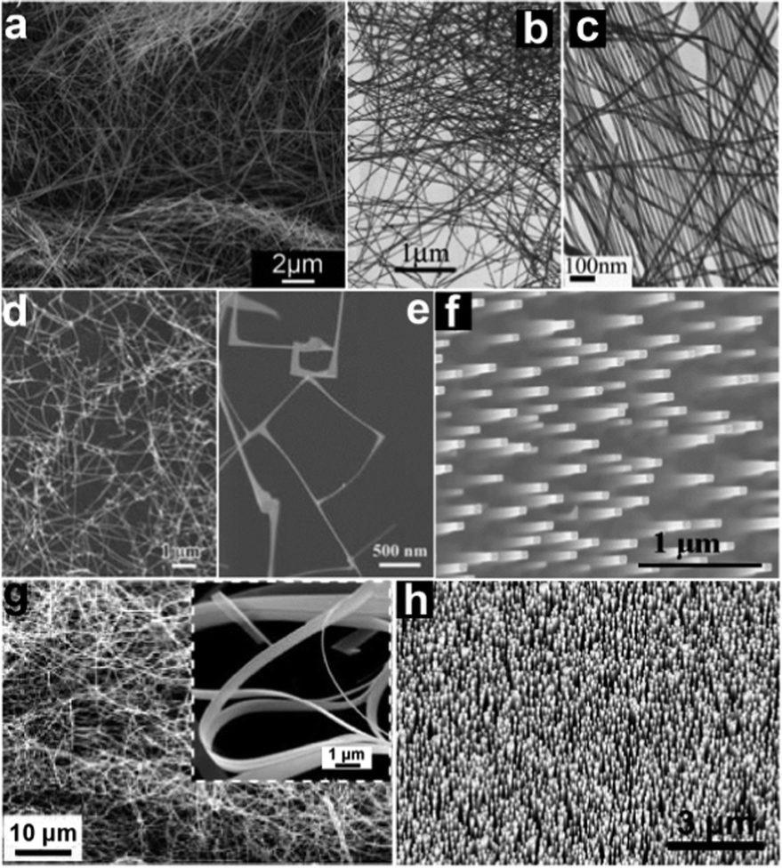 | ||
| Fig. 1 SEM and TEM images of various types of 1-D nanostructures grown from both solution and vapor phase processes. (a) ZnO NWs obtained via hydrothermal method. Reprinted with permission from ref. 74 © 2011, The Royal Society of Chemistry. (b, c) Ag nanocables via hydrothermal method. Reprinted with permission from ref. 76 © 2005, Wiley-VCH. (d, e) In2O3 NW thin films via VLS method. Reprinted with permission from ref. 79 © 2010, Wiley-VCH. (f) ITO NW arrays via an epitaxial growth method. Reprinted with permission from ref. 92 © 2006, Wiley-VCH. (g) SnO2 nanobelts via VS method. Reprinted with permission from ref. 99 © 2003, American Institute of Physics. (h) Well-aligned ZnO NWs via the VS method. Reprinted with permission from ref. 102 © 2005, American Institute of Physics. | ||
Solution phase methods have been extensively explored to synthesize various NWs. Metallic NWs like Ag (Fig. 1b and c), Cu, Au, and Pt76,77 and semiconducting oxide NWs such as ZnO, SnO2, In2O3, Cu2O, Fe2O3 and V2O5 have been successfully synthesized.78 In spite of the decreased crystallinity and weakened electrical properties, it can be predicted that solution phase methods are promising ways for mass production and large scale application of NWs with the advantages of low cost and easy fabrication.
Large aspect ratio often helps to enhance the contact of the electrodes with the active materials in electronic devices like transistors.79 It also facilitates the adsorption–desorption of O2 in optoelectronic devices such as photodetectors.80 That is why NWs find such a wide application in nano-devices. However, it is usually a challenge to synthesize uniform NWs, especially highly ordered NW arrays, by using general hydro/solvothermal methods. In this case, templates are adopted to control the material's growth in a confined domain or along a specific direction. Among all the adopted templates, anodic aluminium oxide (AAO) membranes are widely utilized. As a typical example, highly ordered CdS NWs arrays with lengths up to 1 μm and diameters as small as 9 nm have been obtained by using AAO templates. During the process, CdS was electrochemically deposited into the pores of AAO films from an electrolyte containing Cd2+ and S in dimethyl sulfoxide and the deposited material was found to be hexagonal CdS with the crystallographic c-axis preferentially oriented along the length of the pore.81 A similar method was also employed to synthesize several other 1-D nanostructures, such as In2O3, SnO2, Fe2O3 and Fe3O4 NWs.79,80–84
For the vapor phase processes, an important one is using catalysts to guide the growth of NWs that is generally described as the vapor–liquid–solid (VLS) method.85 In the VLS growth process, metal droplets, usually formed by annealing a gold thin film prepared by sputtering (1–10 nm) or gold colloids,86 are indispensable to serve as catalysts. These metal droplets capture the source vapor and form liquid alloy droplets; then, supersaturation and nucleation occur at the liquid/solid interface and lead to axial crystal growth. Owing to the catalysis mechanism, the NWs often have diameters equal to the droplets, and only grow at sites activated by metal droplets. The VLS method was first developed by Wagner and Ellis to synthesize single crystal Si NWs and has become one of the most successful approaches for the preparation of various kinds of NWs,87 including element semiconductors like Si and Ge, metal oxides like ZnO and In2O3 (Fig. 1d and e), II–VI group semiconductors like ZnS and CdSe, III–V group materials like GaAs and InP, and others.88–91
Using an appropriate substrate, well-aligned NW arrays can be fabricated with the orientation normally perpendicular to the substrate surface through catalyzed epitaxial growth. For example, vertically aligned tin-doped indium oxide (ITO) NW array has been synthesized using an ITO thin film as the substrate, as shown in Fig. 1f.92,93 Besides the ability to tune the diameters of NWs by changing the catalysts' sizes, one of the advantages of the VLS method is the possibility to control the orientation, position and density of NW arrays that are very important to the assembly of NWs for device applications, through patterning the catalyst nanoparticles. Combining the epitaxial growth technique and nano-scale patterned metal catalysts fabricated by electron-beam lithography, photolithography, mask lithography by porous alumina or nanosphere lithography, highly ordered vertical aligned ZnO NW arrays with different densities have been successfully synthesized in hexagonal, orthogonal or other kinds of arrangements.94,95
In addition, different kinds of heterostructures along axial or radial directions are also available through clever synthesis strategies. Branched NWs can be fabricated using a two-step VLS growth method, which has been utilized for SnO2 hierarchical NWs.96 Besides, NWs can be formed with different materials in the core–shell layout by controlling the growth conditions to induce homogeneous reactant decomposition on the core NW surface.97 Through the repeated modulation of reactants, even multishells can be obtained. Axial heterostructures have also been formed by the time-dependent modulation of NW composition and doping during the growing process. These heterostructured NWs are essential for many potential applications in nanoscale optoelectronic devices.
Another process related to the VLS method that has also been employed in the growth of NWs is named vapor–solid (VS) technique. The VS technique does not require metal droplets serving as catalysts. Meanwhile, a higher temperature is usually needed to overcome the much higher activation energy when compared with the VLS method.63 Metal oxide NWs such as ZnO,98 SnO2 (Fig. 1g),99 In2O3,100 CdO101 and many other NWs have been successively synthesized via the VS process in recent years, demonstrating its universality towards various NWs. In catalysts-assistant growth, the remains of catalysts or additives will unavoidably influence the purity of the final products; therefore, the fundamental properties of the materials will inevitably be affected. NWs synthesized via the VS process may also have high crystallinity and outstanding microstructure. For example, Zhang et al. have reported a simple vapor solid deposition approach to synthesize well-aligned ZnO NWs on c-oriented ZnO thin films using Zn as the vapor source.102 As shown in Fig. 1h, well-aligned NWs are in high density and are uniformly distributed over the substrate.
2.2 NW assembly and device fabrication
Between NW synthesis and device fabrication, a key challenge is the controlled assembly of NWs. In the initial phase of NW device research, studies concentrated mainly on individual devices. NWs are directly suspended in solutions and dropped onto the substrates. Randomly distributed and arranged NWs are obtained after the solutions are volatilized. These individual devices are fabricated to investigate the electrical transport properties of NWs. However, large scale device arrays and integrated circuits are impossible to create using this method due to the disordered arrangement of NWs. In order to overcome this challenge and tap the potential of NWs in flexible electronics, several post-growth techniques are developed. NWs assembly is not the focus of this review and Javey in UC Berkeley and Fan in HKUST have already provided very good reviews focusing on NWs assembly; hence, we only provide a brief introduction on NWs assembly here.One of the earliest approaches to assemble NWs is the fluidic alignment in microchannels. Huang et al. constructed fluidic channels on flat substrates using poly(dimethylsiloxane) (PDMS) mold.103 NW arrays are then assembled by passing suspensions of NWs through these channels. Fig. 2a shows the SEM image of InP NWs assembled on a flat substrate, showing that NWs are aligned along the flow direction. By controlling the flow rate, more than 80% of the NWs can be aligned within ±5° of the flow direction. Combined with surface-patterning methods to modify the surface chemical functionality, the fluid flow can generate well-ordered NW parallel arrays. With the use of a layer-by-layer scheme, this approach can also be used to organize NWs into more complex crossed structures, which are critical for building dense electronic device arrays.
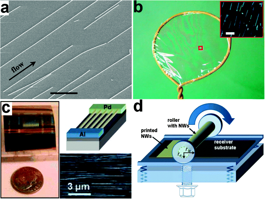 | ||
| Fig. 2 (a) SEM images of parallel arrays of InP NWs aligned by channel flow. Reprinted with permission from ref. 103 © 2001, American Association for the Advancement of Science. (b) Illustration of the blown bubble film NW alignment. Inset shows the dark-field optical image showing Si NWs in the film. Reprinted with permission from ref. 104 © 2007, Macmillan Publisher Ltd. (c) Optical image of a novel diode structure fabricated on parallel arrays of p-Si NWs assembled by the contact printing method. The upper right corner shows the schematic of the Pd-Al contacts and the lower right corner shows the regular array assembly of single Si NWs. Reprinted with permission from ref. 107 © 2008, American Chemical Society. (d) Schematic of the differential roll printing setup. Reprinted with permission from ref. 109 © 2007 American Institute of Physics. | ||
NWs can also be organized within blown-bubble films. The shear stress created by expanding the NW suspension bubble is utilized by Yu et al. to align the high aspect ratio NWs along the principle direction of strain, as shown in Fig. 2b.104 In this approach, a homogeneous polymer suspension of NWs is first prepared and then expanded using a circular die to form a bubble at the controlled pressure and expansion rate. The shear force formed during the expansion leads to the alignment of NWs. The aligned NW density can also be controlled by the concentration of suspensions. The organized NW blown-bubble film can be transferred to flexible plastic sheets as well as highly curved surfaces, showing great potential for large area flexible electronic applications.
Other methods to assemble NWs include the Langmuir–Blodgett (LB) technique and field-assisted orientation. The LB technique is widely used to deposit organic monolayers from a liquid surface to a solid substrate. In order to form NW monolayers, NWs are first functionalized with the surfactant and dispersed on the water surface. When the NWs are compressed, they will organize as parallel arrays with their longitudinal axes perpendicular to the compression direction. Magnetic field is also utilized by Hangarter et al. to assemble NWs.105 However, their methods are limited to metallic or magnetic NWs. In another way, Freer et al. used a dielectrophoretic approach to achieve 98.5% yield of single NWs assembled over 16000 patterned electrode sites with submicrometer alignment precision. By carefully controlling the hydrodynamic and dielectrophoretic forces, single NWs can be assembled on each pair of electrodes with high probability.106
Recently, a new NW assembly approach called contact printing has drawn considerable attention, having the advantages of high efficiency, large scale applicability and compatibility with printing electronics. As shown in the lower right corner in Fig. 2c, the alignment of NWs is realized by directionally sliding the grown substrate with a dense “lawn” of NWs on top of the receiver substrate coated with a patterned photoresist. During the process, NWs are anchored on the receiver substrate by contacting and aligning by the sliding step. Multilayer NWs were assembled by Javey et al. using this approach and used as building blocks for three-dimensional, multifunctional electronic devices.107 Fan et al. improved this dry transfer method by introducing a lubricant during the transfer process, which serves as a spacing layer between two substrates and minimizes the friction between NWs.108 As a result, the uncontrolled breakage and detachment of NWs are prevented and highly ordered NW arrays are obtained. The printed NW density can also be modulated by appropriate surface chemical modification. Both dense and single NW arrays can be aligned through pre-patterning the receiver substrates. To further extend this approach for scalable and large area applications, a differential roll printing (DRP) process is developed. As shown in Fig. 2d, an important aspect of this strategy, as compared to previous methods, is the use of a cylindrical grown substrate.109 NWs are deposited using the VLS process on glass or quartz tubes. The grown tube is then used as the roller and brought into contact with the pre-patterned receiver substrate. By rolling the tube with a controlled velocity, NWs are detached and transferred to the receiver substrate. This process provides a new approach for NW transfer and assembly in a cost-effective and large area manner.
Electrospinning is an efficient technology to fabricate randomly oriented and coiled NWs on certain substrates. A modified electrospinning method was introduced to print large-area organic semiconductor NW arrays uniformly with the desired orientation and position.110–112 This kind of method has many outstanding advantages: (1) it fits for different types of NWs, such as organic NWs arrays with poly(3-hexylthiophene) (P3HT) and poly(ethylene oxide) (PEO) as the precursors, etc. (2) Semiconductor NW arrays can be successfully printed on almost any kind of substrate, such as SiO2/Si, flexible polyarylate (PAR) or even common paper. (3) High-speed and large-area printing is another attractive advantage of this method. (4) The diameter of the NWs, the distance between NWs, and the NW density can be precisely controlled. All these advantages guarantee highly significant device fabrication work on the following steps, and a piece of typical work based on this method will be fully discussed in the following transistor section.
The successful synthesis of NWs and printing of NWs arrays make it possible to fabricate flexible electronic devices. The fabrication process for flexible electronic devices is similar to that of rigid electronic ones, that is, photolithography process followed by micro/nano-electrode metallization and lift-off. First, traditional photolithography is used to pattern contact areas onto both the ends of the NW or NW arrays. Specifically, after NWs growth and assembly on the flexible substrate, the photoresist (positive or negative) is spin coated onto the substrate followed by exposure using UV lithography machine with a patterned photolithography mask. The photoresist over unwanted areas is then removed using the developing solution. Then, the metal film is evaporated over the surface and the remaining photoresist is removed using acetone. At last, the electrodes over the contact areas are annealed at a proper temperature in an inert atmosphere to enhance the contact between the NWs and the electrodes. This photolithography, metallization and lift-off processes have shown themselves to be very resourceful for the fabrication of various flexible electronic devices before. For example, by adjusting the electrode materials, symmetric or asymmetric contacts between the NWs and the electrodes can be obtained. Fig. 2c shows a Schottky diode with asymmetric PA-Al contacts at different ends of the NWs, that is, the Pd forming a near Ohmic contact to the valence band and Al resulting in a Schottky interface. Besides, by adopting different modes of electrodes (T-shaped gate, top-gate, Ω-gate, etc.), by changing different dielectric films, by improving the surface passivation quality, or even via e-beam lithography techniques, a more sophisticated flexible device with smaller sizes can be fabricated.
3 Inorganic NWs based flexible electronic devices
Because organic materials can be formed into NWs with excellent flexibility, it is necessary to give a brief introduction on flexible electronics based on organic NWs, with a focus on their advantages as well as disadvantages. Recent reports have demonstrated that organic materials in a 1-D structure ranging from nanotubes to NWs can be really used for various applications in flexible electronics.113–117 These 1-D structures can be grown or fabricated by both bottom-up or top down strategies. For example, Fig. 3a gives a detailed description of the home-built printer used to print organic NWs.110 In this electrospinning process, organic precursors were injected through a metal nozzle at a predefined rate. An x–y stage driven by a high-speed motor served as the collector. When applying a high voltage between the nozzle tip and the collector and moving the target substrate along a certain direction at the same time, organic NWs can be well aligned on the receiver substrates with the desired orientation, as shown in the inset. Fig. 3b shows the large-area organic NW based transistors array on a flexible PAR substrate, potentially offering the performance that is required for a new type of electronics along with desired transparency and flexible characteristics. Fig. 3c shows the large-area uniform copper phthalocyanine (CuPc) NWs with proper density and a high degree of orientation on the polyurethane acrylate (PUA) grating substrate, which was an ideal candidate for flexible optoelectronic devices.116 | ||
| Fig. 3 (a) Schematic diagram of organic semiconductor NW printing and inset is the optical image of the well aligned organic NWs. (b) Large-area organic NWs FET array on a flexible PAR substrate. Reprinted with permission from ref. 110 © 2013, Macmillan Publisher Ltd. (c) SEM image of organic CuPc NW arrays. Reprinted with permission from ref. 116 © 2012, The Royal Society of Chemistry. | ||
Organic NWs offer the possibility of direct NWs printing and NW-based flexible devices' integration. Organic NWs have the following advantages. (1) Organic NWs can be synthesized from simple, cost-effective, and scalable processes, which have shown promise for their assembly into functional systems. (2) The physical parameters of organic NWs such as size, orientation, surface states, defects and polarization can be easily controlled. (3) The relatively high degree of transparency has been proven to be very important for designing next-generation flexible electronic devices. For example, “see-through” electronic displays, as a completely new conceptual product, have attracted a lot of attention in recent years. On the other hand, organic NWs still have some drawbacks. (1) The relatively low mobility of organic NWs often leads to poor performance of the final devices, thereby restricting the range of application possibilities. (2) High contact resistance as well as mismatched interfaces between organic NWs and the metal electrodes also lead to the further worsening of the final device's performance. (3) Organic NWs do not enjoy full compatibility with existing IC manufacturing processes because of their poor heat tolerance. (4) If organic NWs are introduced to the large-scale commercial production, organic pollution is an obvious result, and sometimes unavoidable.
As we mentioned in the introduction part that inorganic NWs have several superior features when compared with organic NWs, in the following parts, we will, therefore, give details on flexible electronics based on inorganic NWs, ranging from basic electronic devices such as transistors to sensors, photodetectors and other complicated devices.
3.1 Electrodes
The development of flexible electronics requires high quality electrodes with a combination of high electrical conductivity and high flexibility, as well as optical transparency. Indium tin oxide (ITO) is the commonest choice for most current flexible nanodevices because of its high transmittance and conductivity. However, considering the scarcity of indium and the brittlement of ITO film, a new class of conducting material that can replace the ITO film should be designed. Recently, uniform conducting films such as carbon nanotube films, graphene films and especially metal NW films have been employed as stretchable and foldable conductors. For example, Madaria et al.118 fabricated Ag NWs electrode using a dry transfer printing technique on flexible polyethylene terephthalate (PET) substrates. The obtained conducting films show strong adhesion to a PET substrate over a large area with a low sheet resistance of 10 Ω sq−1 and transparency of 85%, comparable to the conventional ITO films. Such a process also allows the preparation of high quality patterned films of silver NWs with different line widths and shapes, allowing the possible application of flexible electronic circuits. Details about the preparation of Ag conducting film were illustrated in Fig. 4a–c. Another example is the use of a Meyer rod coating method for the fabrication of Ag NWs based transparent electrodes.119 Ag NWs ink in a methanol solution with a concentration of 2.7 mg mL−1 was prepared as the coating agent. As shown in Fig. 4d–f, pre-sonicated Ag NWs ink is dropped onto a PET substrate. Then, a Meyer rod is either pulled or rolled over the solution, leaving a uniform, thin layer of NWs network. After drying the film at a proper temperature, Ag NWs based electrodes with specular transmittance of ∼80% and with sheet resistance of 20 Ω sq−1 can be achieved. Such a method is also applicable for other transparent metal NWs electrodes, such as copper,120 a metal with the electrical resistivity almost as good as that of silver. | ||
| Fig. 4 (a) Schematic illustration of the transfer process of Ag NW networks from growing AAO substrate to the PET or glass substrate. (b, c) Photograph of a NW film on PET substrate and SEM image of the network, respectively. Reprinted with permission from ref. 118 © 2010, © Springer. (d–f) Schematic illustration of Meyer rod assisted coating method for Ag electrodes. Reprinted with permission from ref. 119 © 2010, American Chemical Society. | ||
3.2 Transistors
A field-effect transistor (FET) is the most important and basic component in electronics. NWs have been widely investigated recently as the building blocks for flexible FETs, such as silicon, metal oxides and other compound semiconductors. To meet the demand for high speed devices, inorganic semiconductor NWs with high mobility are desired. Flexible InAs NW array FETs working on radio frequency were demonstrated by Takahashi et al. (Fig. 5a and b).121 The high-frequency performance of the InAs NW array FETs were analyzed by measuring two-port scattering parameters (S parameters) in the common-source configuration over a frequency range from 40 MHz to 10 GHz. Derived from these S parameters, the current gain (h21), maximum stable gain (MSG), and unilateral power gain (U) extracted from the measured S parameters as a function of frequency are shown in Fig. 5c. The InAs NW FETs exhibit an impressive maximum frequency of fmax = 1.8 GHz and a cutoff frequency ft = 1.08 GHz. At 1 GHz, the MSG reaches ∼6 dB, indicating that designing an RF amplifier in the gigahertz region is plausible based on InAs NW FETs. The high-frequency response of the devices is due to the high saturation velocity of electrons in high-mobility InAs NWs. More importantly, the InAs NW FETs do not exhibit significant electrical degradation even when bent to a radius of ∼18 mm, showing excellent mechanical flexibility. The unique characteristics in terms of the large on-current (Ion), large transconductance (gm), high mobility and impressive maximum frequency from the InAs FETs pave the way to develop next-generation high-performance semiconducting elementary units for multifunctional optoelectronic device applications in the future.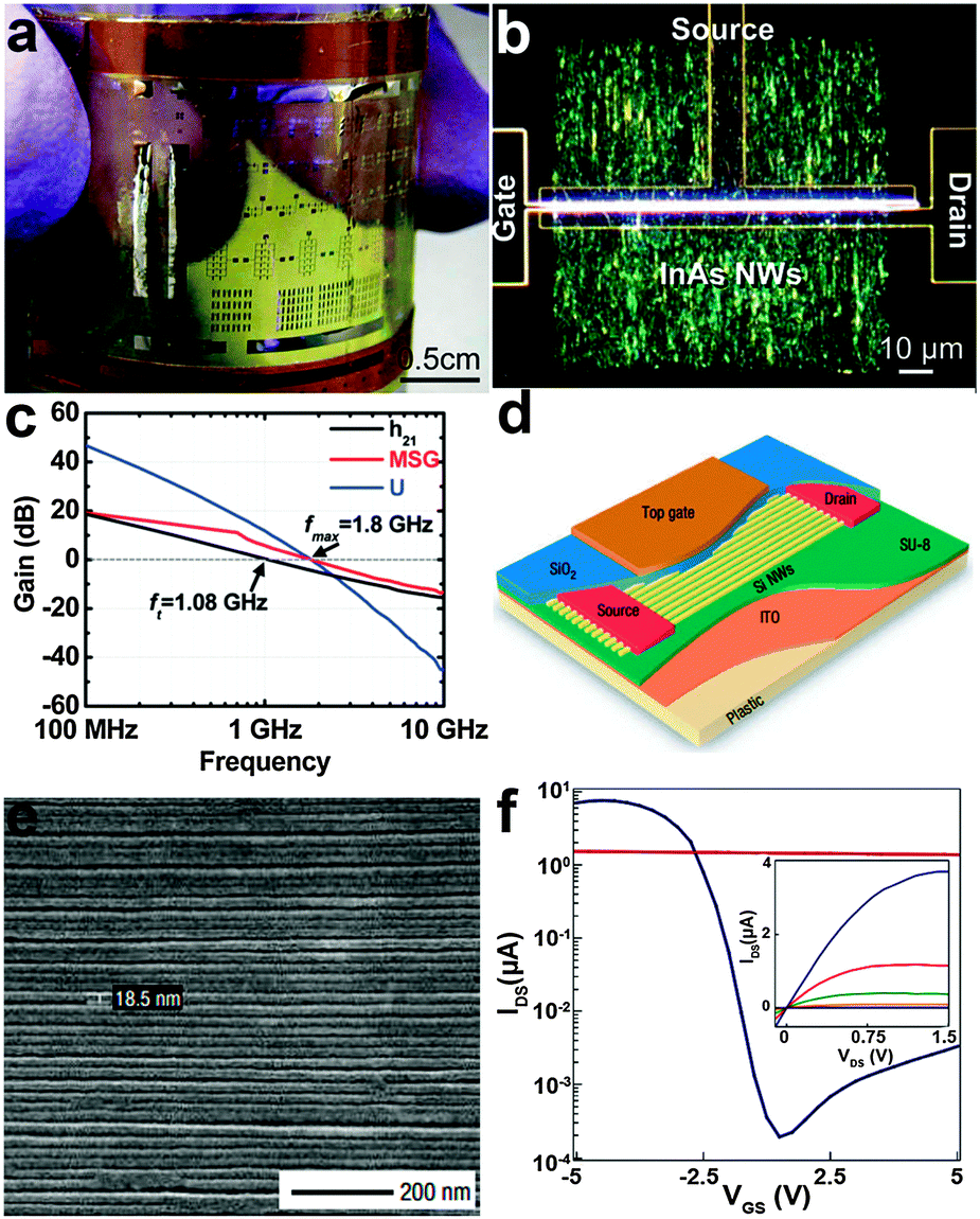 | ||
| Fig. 5 Optical image of (a) the printed InAs NW array FET fabricated on a flexible PI substrate and (b) the InAs NW region. (c) High-frequency behaviour of the InAs NW array FET. Reprinted with permission from ref. 121 © 2010, American Chemical Society. (d) Schematic illustration of the p-type Si NWs array based TFT and (e) the SEM image of the aligned NWs. (f) IDSversus VGS (VDS = 1 V) for a p-type Si NWs array based TFT. Inset is the IDSversus VDS curves correspond to VGS = −5, −4, −3, −2, −1 and 0 V. Reprinted with permission from ref. 122 © 2007, Macmillan Publisher Ltd. | ||
In order to build power-efficient flexible logic gates and integrated devices, both n-type and p-type semiconductor NWs are required. However, most of the currently investigated NWs are n-type semiconductors. Flexible p-type NWs FETs are rarely reported. Doping is the first-thought routine to modify the conducting type of NWs that are used in flexible FETs, from n-type to p-type. Mcalpine et al. present a scalable and parallel process for transferring hundreds of pre-aligned p-type silicon NWs onto plastic to yield highly ordered films for flexible FETs.122Fig. 5d shows the schematic illustration of flexible FETs with the electrodes and various labeled layers. Plastic served as a bendable substrate and 2 μm-thick SU-8 epoxy was used as a gate dielectric in this device. Fig. 5f shows the electronic performance of the top-gate FETs containing about 200 p-type Si NWs. The inset of Fig. 5f shows the Ids–Vds curves at different Vgs from 0 V to −5 V, with negatively increasing gate voltage: the conductance of the device was gradually suppressed, demonstrating the p-type nature of the B-doped Si NWs.
Another interesting work on flexible p-type FETs are PbSe NWs FETs encapsulated in polymethyl methacrylate (PMMA).123 PbSe NWs were aligned under an electric field on varying dielectric stacks and fabricated into flexible FETs operated on kapton films, and aluminum oxide (30 nm) was used as the back gate dielectric and octadecylphosphonic acid (ODPA) was used to passivate the aligned NWs. The obtained device exhibited ambipolar characteristics, as evidenced by the electron transport in the Ids–Vgs curves. A predominantly p-type nature under a negative bias voltage was observed; moreover, a predominantly n-type nature for positive gating was also confirmed by the ambipolar characteristics of this PbSe device. Contrary to the colloidal PbSe NW (NW) and nanocrystal (NC) FETs, this PMMA encapsulated PbSe NW arrays showed a fairly low hysteresis value (<1 V).124
3.3 Sensors
With controllable geometry and high surface areas, NWs exhibited excellent response to outer environments, such as optical radiation, temperature variation, pressure differential, chemical molecules, pH value, proteins and DNA.125 In this section, we highlight several recent significant results that have made impacts on the field of flexible and stretchable sensors, including photodetectors, stress sensors and artificial skins.NW networks, or NW thin films, are emerging as promising structures for photodetectors as their advantages include easy device fabrication process. High performance photodetectors can be fabricated on various NWs thin films such as ZnO, SnO2, In2O3, and multicomponent metal oxides. For example, Yan et al. synthesized Zn2GeO4 NW networks and fabricated efficient ultraviolet photodetectors on a SiO2/Si substrate by using the photolithography technique.134,135 However, expensive and tedious photolithography techniques were required in Yan's work, which would certainly act as a hurdle in the practical applications of NW networks based photodetectors. Recently, flexible photodetectors were fabricated on Zn2GeO4 and In2Ge2O7 NW networks, as shown in Fig. 6. High quality single crystalline Zn2GeO4 and In2Ge2O7 NW networks were synthesized via a conventional CVD method. By simply transferring the NW mats to a transparent adhesive PET tape and printing the silver paste as parallel lines (which served as electrodes), flexible photodetectors were successfully fabricated. Both Zn2GeO4 and In2Ge2O7 NW networks based flexible photodetectors exhibited excellent photoconductive performance in terms of high sensitivity, excellent stability, and fast response and recovery time to the UV light.
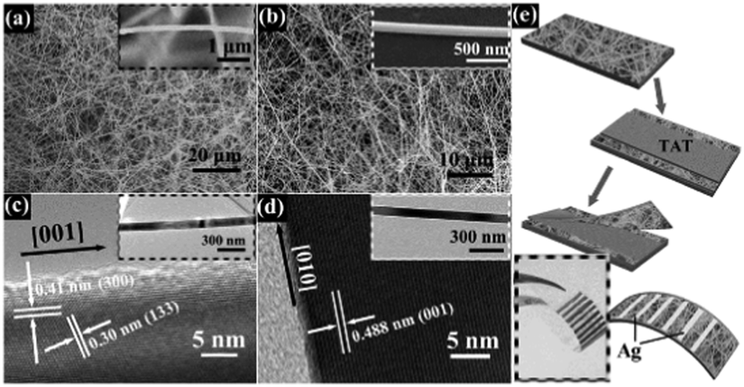 | ||
| Fig. 6 SEM images of (a) Zn2GeO4 and (b) In2Ge2O7 NW networks prepared for flexible photodetectors. (c, d) TEM images of these two as-synthesized NWs, respectively. (e) NW networks transfer and flexible device fabrication process for a representative photodetector based on PET substrate. Reprinted with permission from ref. 38 © 2012 Optical Society of America. | ||
Single NW based photodetectors are the most common NW based optoelectronic devices. They can be easily fabricated via UV photolithography or e-beam lithography techniques followed by metal film deposition techniques. A single NW photodetector is thought to be the most effective, which could directly and quantitatively study light acquisition as well as the optical-to-electrical conversion process. As an example, single ZnTe NW based flexible photodetectors were recently reported.56 ZnTe NWs (Fig. 7a) exhibited p-type conductivity with an effect mobility of 11.3 cm2 V−1 s−1 and the corresponding flexible photodetectors were proven to have the features of excellent flexibility, stability and sensitivity to visible incident light. As shown in Fig. 7b, the flexible device has very stable photocurrent-switching behavior under different light irradiance conditions, indicating its sensitivity to very slight variations in the incident light. In Fig. 7c, the device was bent to different curvature radii to precisely assess the optoelectronic performance of the device. The photocurrents were maintained at about 30 ± 1.2 nA and the on/off ratio stayed at the level of 98 ± 4 under certain test conditions. Besides, Fig. 7d shows the I–V curves of the flexible ZnTe photodetectors after 50, 100, 150, 200 and 258 cycles of bending; no obvious current degradation was recorded, indicating the mechanical robustness and electronic stability of the flexible device.
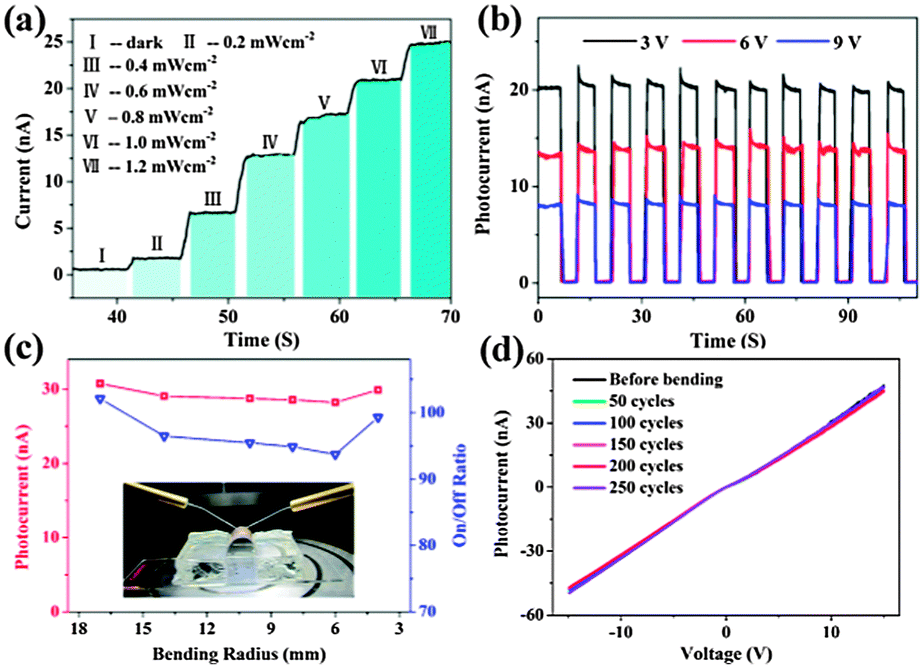 | ||
| Fig. 7 (a) Photoresponse of the flexible ZnTe NWs photodetector under an improved incident light level and (b) at different bias values under the same illumination (532 nm, 1.2 mW cm−2). (c) The magnitude of photocurrents (red) and the corresponding on/off ratio (blue) under different bending radii. Inset shows the optical micrograph of the experimental setup. (d) I–V curves measured before and after different bending cycles. The operation voltage of Fig. 5(a) and 6(c) are 12.5 V and 9 V, respectively. The light intensity of (c, d) is 1.4 mW cm−2. Reprinted with permission from ref. 56 © 2013 Optical Society of America. | ||
An ordered NW array is a simple and efficient remedy for low-level photocurrent faced in single NW based photodetectors. Many technical methods have been summarized above to design arranged NWs, and the obtained NW arrays could be transferred to the flexible substrate directly for the fabrication of flexible nanodevices. In the report of Bai et al., integrated ZnO NW UV photodetectors were fabricated on rigid glass and flexible PET substrates at the macroscopic scale.136 As shown in Fig. 8a and b, cross-finger shaped Ag electrodes were pressed onto the aligned ZnO NWs and provided an Ohmic contact between the Ag electrodes and the ZnO NWs on the PET substrate, which is confirmed by the I–V measurements in Fig. 8c. We can find that the photocurrent is about five orders of magnitude larger than the dark current, giving a very large ON/OFF ratio. Time-resolved UV photoresponse measurements under UV irradiance of 4.5 mW cm−2 and 3 V bias are shown in Fig. 8d, confirming the ultrahigh ON/OFF ratio. This ultrahigh ON/OFF ratio implies the ability to sense weak UV incident light even in a high noise level environment. Using contact printed aligned NW arrays (Zn3As2, Zn3P2, etc.) as the active materials, different types of high performance flexible photodetectors were also successfully fabricated, with typical response to light irradiation with different wavelengths.137 In fact, flexible NWs array based photodetectors are promising building blocks for next generation stretchable optoelectronic devices. Undoubtedly, more research results and exciting discoveries lie ahead.
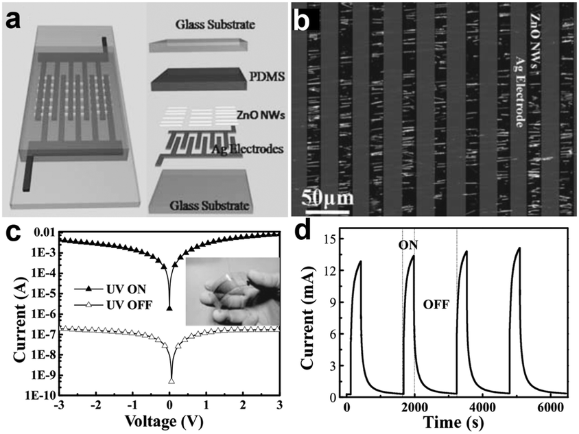 | ||
| Fig. 8 (a) Schematic design of an integrated UV sensor. (b) Optical image of ZnO NWs connected in parallel between Ag electrodes. (c, d) I–V curves and time-dependent photoresponse of the flexible UV sensor with/without UV illumination, respectively. Inset of (c) is the optical image of a flexible integrated NW UV sensor. Reprinted with permission from ref. 136 © 2011, Wiley-VCH. | ||
Technically, the Si-NW bridges on a SOI substrate adhered on the outer surface of a steel plate is not a precise flexible stress sensor, but a means of estimation in strain/stress and pressure. Another report on a fully packaged strain sensor device based on a single ZnO piezoelectric fine-wire (NWs, microwires) gives us a vivid description of real flexible stress sensors.139 As shown in Fig. 9a, the flexible and optically transparent strain sensor device was fabricated by bonding a ZnO piezoelectric fine-wires laterally on a polystyrene (PS) substrate. Silver paste was applied at both ends of the ZnO wires to fix its two ends tightly on the PS substrate while serving as the source and drain electrodes. Further, a thin layer of polydimethylsiloxane (PDMS) was introduced to package the device. The I–V behaviors of the sensor device were measured under various strains, as shown in Fig. 9b. We can see that the I–V curves shift upward with tension strain and downward with compressive strain under various strain values. Besides, the current response of the sensor over many cycles of repeated compressing and stretching were also tested, and the results are recorded in Fig. 9c. Fig. 9d shows the partially enlarged drawing. The highly regular response curves indicate the high reproducibility and good stability of this kind of flexible sensor device. Gauge factor, which is the key parameter for a practical strain sensor, is defined as [ΔI(ε)/I(0)]/Δε, where Δε and ΔI(ε) are the amount of variation change of strain and the corresponding current. The highest gauge factor demonstrated for this kind of flexible stress sensor device is 1250, far exceeding the conventional doped-Si strain sensor (∼200). The outstanding performance of this flexible strain sensor based on ZnO nano/microwires shows its good application future in strain and stress measurements in the fields of science and technology.
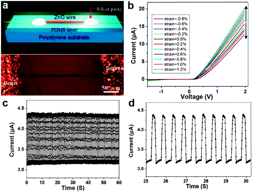 | ||
| Fig. 9 (a) Schematic (up) and optical image (bottom) of the flexible single ZnO based strain sensor device. (b) Typical I–V curves of the sensor at different strain conditions. (c, d) Current response of the flexible stress device that was repeatedly stretched at a frequency of 2 Hz under fixed bias of 2 V. Reprinted with permission from ref. 139 © 2008, American Chemical Society. | ||
 | ||
| Fig. 10 (a) Schematic of the pressure-sensitive organic field-effect transistors device that uses a microstructured PDMS film as the dielectric layer. (b) Optical image of the aluminium-coated microstructured PDMS film, indicating the high flexibility of the dielectric layer film. (c, d) Pressure response of the pressure-sensing organic single-crystal transistors based on the microstructured PDMS dielectric layer. (e) Flexible 8 × 8 pixel pressure sensor arrays fabricated by sandwiching the microstructured PDMS film between two PET substrates. (f) The pressure response to an above-placed tripod. Reprinted with permission from ref. 140 © 2010, Macmillan Publisher Ltd. | ||
Parallel NW arrays were proven to be promising candidates for flexible and robust artificial skin, as reported by Takei et al.141 In their work, macroscale (7 × 7 cm2) integration of parallel NW arrays as the active-matrix backplane of a flexible pressure-sensor array were reported, as shown in Fig. 10b and 11a. Laminated pressure-sensitive rubber (PSR) is used as the sensing element and the source electrodes of printed Si/Ge NW-array based FETs (inset of Fig. 11a) are connected to drive the PSR. With variations of external pressure, the conductance of PSR rises or falls, leading to the different modulation index of the NW FETs and eventually results in the specific output signal of the pixel. By setting a certain frequency of the applied pressure, the corresponding time dependent output electrical signal of a pixel could be obtained. Fig. 11c shows the conductance-pressure profile with a frequency of 5 Hz, indicating the fast and stable response of this stress sensing unit. Finally, a 19 × 18 pixels array based artificial skin was successfully fabricated, as shown in Fig. 11d. A normal pressure of ∼15 kPa was applied on the surface of a ‘C’ shaped PDMS film that covered the artificial skin. By measuring the conductance of each pixel and introducing normalizations, the authors formulated the two-dimensional intensity profile (Fig. 11e). The contrast represents the normalized output signal, with the blue pixels representing the defective points. The character ‘C’, corresponding to the applied pressure area, illustrate the stable response of this flexible artificial skin. The uniform assembly of ordered Ge/Si NW arrays ensured the outstanding mobility of (∼20 cm2 V−1 s−1) NW-array FETs and provided superb mechanical flexibility of the flexible artificial skin. NW also exhibits the single-crystalline nature, which could help in the low-voltage operation mode for the sensor circuitry. All these attributes make the parallel NW arrays an ideal choice for more sophisticated artificial skin.
 | ||
| Fig. 11 (a) Schematic of the passive and active layers of NWs based artificial skin. (b) Optical image of the individual stress sensing pixel. (c) Time dependent output signal for an applied pressure frequency of 5 Hz. (d) As-fabricated 19 × 18 pixel array artificial skin with a ‘C’ shaped PDMS mould placed on the top for applying pressure. (e) Corresponding two-dimensional output signal profile. Reprinted with permission from ref. 141 © 2010, Macmillan Publisher Ltd. | ||
Although the above work demonstrated the fulfillment of artificial skin with NW arrays, it only involved the integration of pressure sensors with an NW based electronic readout circuit. It was very inconvenient to obtain an intuitive grasp on the performance of the flexible artificial skins, as the output of each pixel was individually measured and then statistically analyzed. Considerable progress was recently obtained by Wang et al., who designed a user-interactive artificial skin that not only spatially maps the applied pressure but also provides an instantaneous visual response through a tricolour OLED pixels array.142 This artificial skin basically consists of three parts, namely pressure-sensitive rubber, active-matrix backplane circuitry and OLED arrays. As shown in Fig. 12a, each sensing and display pixel consists of a TFT, an OLED and a PSR integrated vertically on a polyimide substrate. The enlarged optical micrographs of one pixel is shown in Fig. 12c, where we can see that the drain of the TFT is connected to an ITO pad that serves as the anode electrode for the corresponding OLED, while the cathode of each OLED is connected to the ground through the PSR. Fig. 12b illustrates an entire 16 × 16 pixels array of pixels, in which the scan lines (5/35 nm Ti/Au back-gate electrodes) and data lines (0.5/40 nm Ti/Pd source–drain contacts) are connected to 5 and 10 V, respectively, as shown in Fig. 12d. In Fig. 12e, letter shaped PDMS slabs were placed onto the PSR and uniform external force was applied on the PDMS slabs. The conductivity of the PSR increased accordingly and subsequently resulted in the underlying OLED turning on. A uniform performance of each TFT and single-pixel OLED allowed the pressure signal to be both spatially mapped and visually seen, as corresponding C-, A- and L-shaped bright light emitting areas were clearly recognized on the OLED panel (Fig. 12e, right). Besides, the color of the OLED can be effectively tuned by applying different emissive layer materials and the brightness of each OLED can also be sensitively controlled by the magnitude of the local pressure. Although the spatial resolution is far from usable in practical applications, this flexible artificial skin still demonstrated the practicability of user-interactive sensing system. By further improving the pixel integration level and using multiple sensor components, a superior kind of artificial skin that enables more sophisticated bionic operations can be successfully planned.
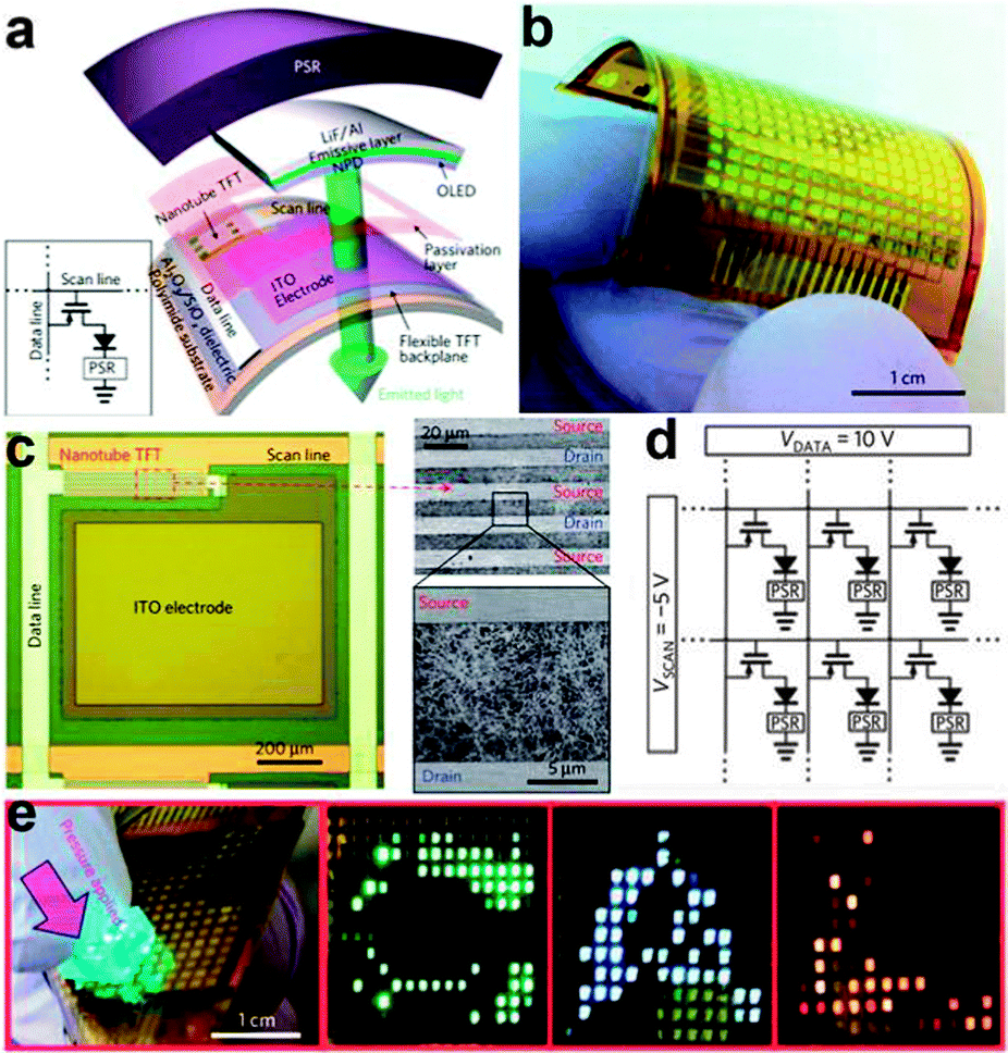 | ||
| Fig. 12 (a) Schematic illustration of the user-interactive artificial skin. LiF/Al is the cathode that connects the PSR to each pixel of AMOLED. (b) Photograph of a fabricated device (16 × 16 pixels) artificial skin. (c) Enlarged view of the active area. (d) Circuit schematic of the artificial skin matrix. (e) As-fabricated 16 × 16 pixel array artificial skin with ‘C/A/L’ shaped PDMS slabs placed on the top for applying pressure. Reprinted with permission from ref. 142 © 2013, Macmillan Publisher Ltd. | ||
3.4 Display devices
As an important display component, light emitting diodes have developed rapidly in the recent years. NWs based on various semiconductors offer the added advantage of high material quality leading to improved device performance. Basically, research in the area of NW based display components was focused on two aspects.On one hand, semiconductor NWs were used as the optically active component in display devices. Individual gallium nitride (GaN) NWs have been configured as UV-light-emitting diodes on flexible plastic substrates by Lieber's group.143 In this report, the authors assembled crossed n-type GaN NWs and p-type Si NWs onto a plastic substrate to form flexible crossed-NW LEDs, as shown in Fig. 13a and b. This kind of n-GaN/p-Si crossed diodes not only exhibited stable emission (Fig. 13c) but also could maintain their emissive properties upon repeated cycles of bending. In another work, vertically oriented ZnO NWs were fabricated into a highly flexible light-emitting device.144 From the design scheme in Fig. 13d, we could see that the flexible LED was composed of four layers, namely, supporting (PET/ITO) substrate, vertically oriented ZnO NWs layer, insulating polystyrene (PS) film and the hole-injection anode layer. In particular, the hole-injection anode layer consisted of a thin poly(3,4-ethylene-dioxythiophene) poly(styrenesulfonate) (PEDOT:PSS) layer and an evaporated Au film. Fig. 13e and f show the overall image of the active ZnO NWs layer. All the NWs showed a uniform size with typically ∼2 μm length and 70–120 nm diameter. With or without Al doping, this diode structure showed excellent optical emission performance in the range of 500–1100 nm (Fig. 13g). These results suggest that semiconductor NWs could serve as high-performance building blocks for future lightweight display devices.
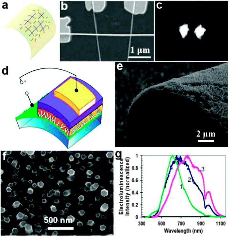 | ||
| Fig. 13 (a) Schematic and (b) SEM image of a crossed-NW LED array on a flexible plastic substrate, in which p-SiNWs are vertically aligned and GaN NW is horizontally aligned. (c) Electroluminescence (EL) images of localized emission from forward-biased Si–GaN junctions. Reprinted with permission from ref. 143 © 2003, American Chemical Society. (d) Scheme for a flexible LED structure consisting of vertically oriented ZnO NWs grown on a polymeric ITO-coated substrate. (e, f) SEM images of the ZnO NWs grown on a planar transparent substrate and on a bent Au film, respectively. (g) Normalized electroluminescence spectra versus wavelength based on various LED structures. Reprinted with permission from ref. 144 © 2008, American Chemical Society. | ||
On the other hand, semiconductor NWs were used as the transistor driving circuitry. NW transistor driving circuitry is of particular interest for future display devices because it offers high carrier mobility, optical transparency, as well as mechanical flexibility. Zhou et al. reported high-performance arsenic (As)-doped indium oxide (In2O3) NWs for transparent active-matrix organic light-emitting diode (AMOLED) displays.6 Thin-film transistors (TFTs) based on As-In2O3 acted as the key components of the driving circuitry. The synthesized As-doped In2O3 NWs was shown in Fig. 14a, which have high electron mobility of ∼1490 cm2 V−1 s−1. The as-designed TFTs can be used to generate the driving circuit to control a variable-intensity OLED, as shown in the inset of Fig. 14b. Regulating the input voltage could efficiently control the light intensity of the OLED. Fig. 14c shows the circuit diagram that indicates the physical layout of the connections for the seven-segment AMOLED display. The most important components of this circuitry were the switching transistors (T1), driving transistors (T2), and one storage capacitor (Cst). They were introduced here to select a specified pixel, control the current and store data during one period for time-varying operations, respectively. This fully integrated seven-segment AMOLED display was proven to have good transparency of 40%, as shown in Fig. 14d. The background image could be partly seen through the AMOLED display arrays. The optical images of the seven-segment pixels with lighted numerical digits (Fig. 14e–g) indicated the outstanding and stable performance of the NWs transistor driving circuitry. By changing the ITO glasses with the PET substrate, the authors further proved the successful fabrication of flexible SWNT transistors for LED driving circuitry.49
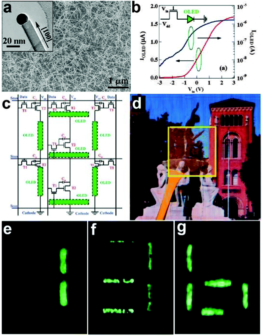 | ||
| Fig. 14 (a) SEM image of As-In2O3 NWs. (b) Output current through the loaded phosphorus OLED (IOLED) versus Vin with Vdd at 5.0 V in linear scale (red line) and log scale (blue line), respectively. (c) Circuit diagram of seven-segment AMOLED display unit. (d) Optical photograph of fully transparent AMOLED display driving circuitry. (e–g) The seven-segment AMOLED display unit displays numbers 1, 3, and 6, respectively. Reprinted with permission from ref. 6 © 2009, American Chemical Society. | ||
3.5 Memories and logic gates
Over the past several years, semiconductor NWs have also represented attractive building blocks for memories and logic gates, which are essential components for the next generation circuits. Traditional memories and logic gates based on silicon have greatly promoted the development of the very large scale integrated circuit (VLSI) technology. However, in terms of flexible devices, for example, that are designed to mount on human skin or planted into internal organs, the constraint of traditional electronic units would certainly limit their potential applications. Therefore, fully flexible memories and logic gates have been greatly welcomed by scientific researchers for NW based electronic devices.Lieber's group first reported the monolithic integration of individual and parallel arrays of germanium–silicon (Ge–Si) core–shell NWs as multilayer flexible circuits.145 As shown in Fig. 15a and b, the final circuit consists of a lower layer of PMOS inverters and an upper layer of floating gate memory elements. From the input–output characteristics of the lower layer of PMOS inverter (Fig. 15c), it was found that these inverters exhibited p-type transfer characteristics with a maximum voltage gain of 3.5. Fig. 15d shows the AC inverter characteristics of the lower layer of PMOS inverters when driven by a 50 MHz sine wave supply of 4 V. At a frequency of 50 kHz, the input signals are ideally inverted to the output signals without any loss. Fig. 15e and f show the current vs. voltage sweeps recorded on the upper layer of the floating gate memory elements. A large hysteresis (i.e. memory window) and stable writing and erasing operation can be observed, respectively, indicating the good memory retention of the floating gate memory elements.
 | ||
| Fig. 15 (a) Schematics and circuit diagrams of inverter (top) and floating gate memory (bottom) elements. (b) Optical image of inverters (layer 1) and floating gate memory (layer 2) on Kapton. (c) DC inverter characteristics. (d) AC inverter characteristics. (e) Hysteresis in current–voltage characteristics of a memory layer element. (f) Switching characteristics of memory at VCG = 5 V with ±15 V pulses (pulsing time: 1 ms). Reprinted with permission from ref. 145 © 2007, American Chemical Society. | ||
Flexible logic gates were also fabricated on the base of well aligned NWs that were generated by top-down fabrication steps.146 By using anisotropic chemical etching steps, Rogers et al. have once obtained GaAs nano/microwires with triangular cross sections from GaAs wafers. A slightly oxidized PDMS stamp was used to transfer the GaAs wire arrays from the original base onto a PET/PU (polyurethane) substrate (Fig. 16a). Simple circuits consist of various logic gates and individual MESFETs on a PET substrate are shown in Fig. 16b and c. Logic functions, such as NOR and NAND, can be performed by these flexible logic circuits. For example, Fig. 16d and e show the scheme of combining two GaAs wire switching transistors with another GaAs wire load transistor to yield NOR logic functions, as the logic status of Vout can only be logic 1 (high positive output voltage) when both inputs are logic 0 (at high negative voltages). Fig. 16f and g show the optical image of circuit diagrams and the voltage transfer characteristics of the NAND gate, respectively. It can be seen that the flexible NAND gate also shows very stable logic operation performance. Furthermore, Rogers and his colleagues have reported a medium-scale integrated digital circuit composed of up to about 100 SWNT transistors fabricated on a flexible plastic substrate.147 This flexible digital circuit could be used to decode a binary-encoded input of four data bits into sixteen individual data output lines. This outstanding ability suggests that well-designed flexible integrated circuits based on NWs could be applied widely in many areas where conventional, rigid circuits cannot meet the requirements, for example, implantable electronics and prosthetics in the near future.
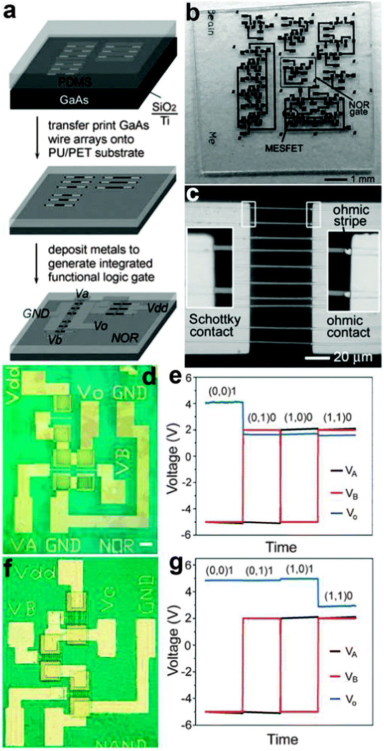 | ||
| Fig. 16 (a) Transfer print process of GaAs wires and logic device fabrication process. (b) Optical images of various logic gates and individual MESFETs fabricated on PET substrates. (c) Magnified optical micrograph of an individual Ti/n-GaAs Schottky diode on the PET sheet. (d, e) Optical images and input–output characteristics of a NOR gate. (f, g) Optical images and input–output characteristics of a NAND gate. Reprinted with permission from ref. 146 © 2006, Wiley-VCH. | ||
4 NW flexible energy conversion and storage devices
Accompanied with the development of flexible electronics, great interest has been aroused in integral flexible/bendable electronic equipment such as wearable devices, rollup displays and bendable mobile phones. However, the current energy storage devices containing lithium ion batteries and supercapacitors are usually too heavy, rigid and bulky to match the particular requirements of flexible electronics. Therefore, the trend in the next generation of energy storage devices development is to realize light, flexible and small units with shape-conformability, aesthetic diversity and excellent mechanical properties. NWs with high aspect ratio, fast charge transfer pathways and stable frameworks have attracted increasing research interest in the area of energy conversion and storage. In this section, we review some recent advances that NWs have made in the field of lithium ion batteries (LIBs), supercapacitors (SCs), solar cells, and generators.4.1 Lithium ion batteries
Among the newly emerging energy storage devices, lithium ion batteries (LIBs) are one of the most popular candidates due to their relatively high energy density, long cycling life, good power performance and low cost.148–178 For LIBs, the charges stored are mainly contributed by the intercalation of Li+ on the surface and in the bulk of the active materials, delivering higher energy density (120–180 W h kg−1) than other energy storage devices.148 NWs with a highly elastic structure demonstrated appropriate characteristics for novel flexible LIBs, which are in urgent demand to meet the development and promotion of flexible electronics. Recently, several excellent comprehensive reviews were given to introduce the fast development of flexible LIBs; therefore, we will not provide the details here, but only provide a brief introduction in this area.179–182Planar type flexible LIBs are one of the most important and earliest developed batteries. This kind of flexible LIBs has the features of very small thickness, light weight, good energy density and power density, and excellent cycling stability. One good example is the flexible planar LIBs with 3D hierarchical ZnCo2O4 NW arrays grown on a carbon cloth as the flexible electrode.167 As shown in Fig. 17, the 3D nanostructure exhibits a distinct plateau between 0.8 and 1.2 V in the voltage window of 0.01–3.0 V and only 16.5% decay of initial capacity (1530 mA h g−1) after 100 cycles (Fig. 17c). The specific capacity is almost constant in the range of about 1200–1340 mA h g−1 with 99% capacity retention from 3 to 160 cycles. Fig. 17d illustrates the typical voltage profiles of the flexible battery device composed of ZnCo2O4/carbon cloth as anode and LiCoO2/Al foil as the cathode by bending it from different directions for hundreds of cycles. The constant capacity, even after 120 cycles of bending, reveals that the electrical stability of the fabricated flexible full battery is hardly affected by external bending stress. The good adhesion and electrical contact between the NWs and carbon cloth, the facile diffusion of the electrolyte and accommodation of the strain induced by the volume change and the 3D hierarchical nanostructures resulted in better performance of the flexible battery. An enhanced power density was achieved once urchin-like ZnCo2O4 NWs were used.172
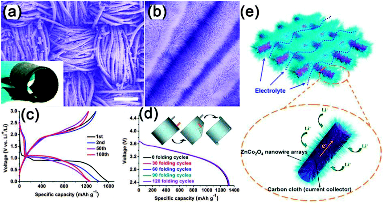 | ||
| Fig. 17 (a, b) Typical FESEM images of the ZnCo2O4 NW arrays grown on a carbon cloth at different magnifications. (c) Typical voltage versus specific capacity profiles for the first, second, 50th, and 100th discharge and charge cycles. (d) Typical voltage versus specific capacity profiles for the first, second, 50th, and 100th discharge and charge cycles. (e) Schematic representation and operating principles of rechargeable lithium-ion battery based on ZnCo2O4 NW arrays/carbon cloth. Reprinted with permission from ref. 167 © 2012, American Chemical Society. | ||
Besides ZnCo2O4 NWs, other metal oxide nanowires were also used to fabricate flexible LIBs. Although these types of planar flexible LIBs exhibit many advantages when compared with conventional rigid LIBs, they still suffer from several drawbacks. For example, the size of planar flexible LIBs is still quite large and the device is too thick, which makes them unfit for integration with other flexible electronic or optoelectronic devices, especially in the case of on-chip integration for microelectronics applications. Besides, this kind of planar flexible LIBs cannot stand a large degree of curving or bending, which also makes it impossible for real flexible electronics applications.
One solution to overcome these problems is to develop ultra-small and stretchable LIBs.183 Stretchability represents a rigorous challenging of mechanical stability. Stretchable devices must bear large strain deformation and large shape deformation, including not only bending but also twisting, stretching, compressing and other forms of deformation. Recently, Rogers et al. developed a very fancy type of highly stretchable LIBs with the active materials segmented design, and unusual ‘self-similar’ interconnect structures between them. The stretchable LIB was fabricated on thin silicone elastomers as substrates, as illustrated in Fig. 18a. As a result, the as-fabricated LIB obtains stretchability of up to 300%, and it still maintains a capacity as high as 1.1 mA h cm−2 at the rate of C/2. Although the output power of the battery decreased slightly with strain resulting from increased internal resistances with strains at these large levels, surprisingly, the stretchable battery could turn on a commercial LED even when it was stretched by up to 300%, as shown in Fig. 18b and c. The high stretchability of the fabricated battery satisfies the requirements of many applications that are being contemplated for stretchable electronics.
 | ||
| Fig. 18 (a) Schematic illustration and exploded view layout of completed stretchable LIBs. (b, c) Lighting a red LED without and with strain. Reprinted with permission from ref. 183 © 2013, Macmillan Publisher Ltd. | ||
Although significant progresses have been made in flexible LIBs, the following items should be considered before their real applications in flexible electronics. First, both the energy density and power density should be further improved to make them comparable with conventional rigid LIBs. Second, it is quite important and sometimes essential to fabricate ultra-small batteries to realize chip-level integration with flexible electronic or optoelectronic devices. Third, more delicate devices should be designed in case of special applications.
4.2 Supercapacitors
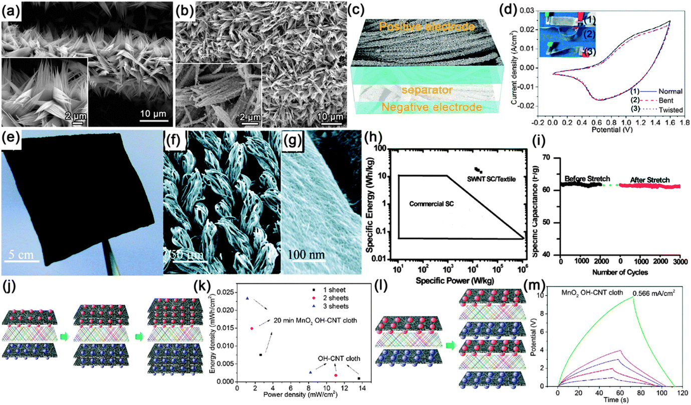
Supercapacitors (SCs), also known as electrochemical capacitors or ultracapacitors, are another kind of vital energy storage devices because of their long cycle life (>105 cycles), high power density (>10 kW kg−1) and high rate capability with fast charge–discharge capability within seconds. Similarly, with the configuration of LIBs, a SC is also composed of an anode, cathode, separator and electrolyte. The working mechanism of SCs can be classified into electrical double layer capacitors (EDLCs) and pseudocapacitors.184,185 Since both the EDLCs and pseudocapacitors are surface electrochemical related devices, high surface area electrode materials are necessary in SCs, fitting well with the features of NWs. Similar with the construction of flexible LIBs, several kinds of flexible SCs have been demonstrated based on NWs (carbon materials, transition metal oxides and conducting polymers), including paper-like SCs, transparent SCs, woven SCs, micro-SCs and fiber SCs, which will be discussed in sequence in the following sections.000 S m−1, served as the scaffold for the incorporation of polyaniline and current collectors. The volume density of the CNTs was only 30%, leaving 70% of the total networks in the form of a porous structure. Even though the thickness of the device was estimated to be only 113 μm, the entire device shows superior mechanical flexibility. At 1.0 A g−1, the discharge specific capacitance of the flexible device is 332 F g−1 based on the total mass of the device, which is only 7.8% smaller than the one in 0.5 M H2SO4 solution (360 F g−1) (Fig. 19b). A high energy density of 7.1 W h kg−1 and a high power density of 2189 W kg−1 were achieved, which is far superior to those of current conventional supercapacitors (Fig. 19d). After 1000 charge–discharge cycles, the device shows good cycling stability with only 8.1% decay and stable Coulombic efficiency ranging from 95.2% to 102.8%. During the time stability test displayed in Fig. 19e, the capacitance shape and redox peaks were effectively retained after 1 week and even 2 months, leading to a much stable device.
 | ||
| Fig. 19 (a) Schematic illustration of the PANI/CNT nanocomposite electrodes effectively solidified in the polymer gel electrolyte and digital pictures that show the all-solid-state device (size ∼ 0.5 cm × 2.0 cm) under normal conditions (top) and its highly flexible (twisting) state under electrochemical measurements (bottom). (b) Comparison of discharge abilities of the flexible PANI/CNT nanocomposite thin film electrodes in the H2SO4–PVA gel electrolyte and in the 0.5 M H2SO4 aqueous solution. The inset in (b) shows one cycle of galvanostatic charge–discharge curves at 1 A g−1. (c) Comparison of CV curves at 5 mV s−1 for the all-solid-state device tested in the normal, twisting and even folded condition, respectively. (d) Ragone plots for the electrode materials and for the entire all-solid-state device. (e) Time life stability of the device. Reprinted with permission from ref. 198 © 2010, American Chemical Society. (f) Schematic of Xerox brand printer paper treatment with PVDF. (g) Photograph of a Meyer rod-coated supercapacitor on Xerox paper. (h) Photograph of ink-jet printed supercapacitor on Xerox paper. (i) Specific capacitance at different current densities. Reprinted with permission from ref. 201 © 2010, AIP Publishing LLC. | ||
Another kind of paper-like supercapacitors can be fabricated by coating conductive and electroactive CNTs or semiconductor NWs onto paper substrates.161,163,201–204 Among the reported achievements, Cui's group has dedicated a lot of efforts on paper-like supercapacitors by using the low-cost Xerox paper as the substrate. For instance, Cui et al. reported carbon nanotube thin film-based supercapacitors fabricated with printing methods, where electrodes and separators are integrated into single sheets of commercial paper.201 Before coating the SWCNT ink on to the paper, the paper substrates were first treated with polyvinylidene fluoride (PVDF) to prevent the penetration of ink into the paper. The schematic illustration is presented in Fig. 19f. Fig. 19g shows a printed supercapacitor using the Meyer rod coating method. For large scale fabrication, an ink-jet printer can be utilized to print any patterns (Fig. 19h). Based on the voltage profile and mass density of SWCNT, the specific capacitance is calculated to be 33 F g−1 (Fig. 19i) at a specific power of 250000 W kg−1. Due to the lightweight SWNT films and the absence of heavy metals, the capacitance of the assembled device could be greatly improved when compared with traditional supercapacitors.
 | ||
| Fig. 20 (a) Photograph of a flexible and transparent supercapacitor fabricated using CNT films. (b) AFM image of entangled CNT networks sitting on a transparent PET substrate. (c) Schematic of a flexible and transparent supercapacitor. The gray color represents a Nafion film as the separator between two In2O3 NWs/CNT heterogeneous film electrodes. (d) Cycle-life data of In2O3 NWs/CNT heterogeneous film electrochemical capacitor measured at 0.5 A g−1. Reprinted with permission from ref. 206 © 2009, AIP Publishing LLC. (e) SEM images of branched nanocup film, where short carbon nanotubes (25 nm in diameter and 330610 nm in length) are branched from the bottom of the nanocup. (f, g) Transparent and flexible natures of the supercapacitor devices. (h) CNC devices are compared with various energy storing devices by the Ragone plot that shows the values of energy density for power density. (SG: single layer graphene, RMGO: reduced multilayer graphene oxide, HGO: hydrated graphitic oxide, LSG-EC: laser-scribed graphene electrochemical capacitor). Reprinted with permission from ref. 208 © 2012, Macmillan Publisher Ltd. | ||
More recently, Jung et al. constructed mechanically flexible and optically transparent thin film solid state supercapacitors by assembling nano-engineered carbon electrodes.208 Through the control of the nanopore dimension in anodic aluminum oxide (AAO) templates and CVD conditions, precisely tailored carbon nanocups can be fabricated, as shown in Fig. 20e. The as-fabricated electrode is highly conductive (117 S m−1) and transparent. After being sandwiched by polyvinyl alcohol–phosphoric acid gel electrolyte, transparent and highly flexible supercapacitors are demonstrated (Fig. 20f and g). With the increasing measured temperature, a high areal capacitance of 1220 μF cm−2 was obtained at 80 °C, which is almost three times than that (409 μF cm−2) at room temperature. The Ragone plot is shown in Fig. 20h. The volumetric peak power and energy densities of the branched carbon nanocup based supercapacitors are 19 mW cm−3 and 47 mW h cm−3, respectively, which is similar to some high performance graphene-based supercapacitors.211
Carbon cloth, as flexible, conductive and stable substrates, has attracted much interest to be used as current collectors in flexible supercapacitors. Our group has devoted some efforts on the development of flexible SCs by using carbon cloth current collectors to support NWs.213,216 For example, we developed asymmetric supercapacitors (ASCs) based on acicular Co9S8 nanorod arrays as positive materials and Co3O4@RuO2 nanosheet arrays as negative materials.213 Acicular Co3O4 nanorod arrays were first grown on carbon cloth, acting as a template for further Co9S8 nanorod arrays growth or RuO2 nanosheets deposition (Fig. 21a and b). The schematic illustration of the as-fabricated ASC is shown in Fig. 21c. Remarkably, the as-fabricated ASCs could be cycled reversibly in the range of 0–1.6 V in an aqueous electrolyte (LASC) and solid-state (SASC) electrolyte. The performance of SASC was preserved after being bended and twisted, demonstrating the desirability of carbon cloth-based current collectors (Fig. 21d). Both capacitors reveal excellent rate performance through five steps of charge–discharge rates, changing successively from 2.5 to 50 mA cm−2. Moreover, high volumetric capacitance of 4.28 F cm−3 for SASC remained at 90.2% even after 2000 charge–discharge cycles. Electrochemical performance with an energy density of 1.44 mW h cm−3 at the power density of 0.89 W cm−3 for SASC was demonstrated.
 | ||
| Fig. 21 (a, b) SEM images of Co3O4 and Co9S8 acicular nanorod arrays grown on carbon cloth. (c) Schematic illustration of the asymmetric supercapacitors utilizing Co9S8–carbon cloth as positive electrode and RuO2–carbon cloth as negative electrode. (d) CV curves of the ASC tested under normal, bent and twisted conditions. Reprinted with permission from ref. 213 © 2013, American Chemical Society. (e–g) Photograph and SEM images of CNT coated cotton cloth. (h) Ragone plot of commercial SCs and SWNT SC on porous conductors including all the weights. (i) The specific capacity for a stretchable SC before and after stretching to 120% strain for 100 cycles. The current density is 1 mA cm−2. Reprinted with permission from ref. 217 © 2010, American Chemical Society. (j) Schematic illustration of the laminated structure of fabric SC. (k) Ragone plot of the laminated capacitors. (l) Schematic illustration of the tandem structure of fabric SC. (m) Galvanostatic charge–discharge curves measured at 0.566 mA cm−2 for tandem MnO2/CNT fabric SC with 1, 2, 3, 4, and 10 unit(s), respectively. Reprinted with permission from ref. 220 © 2013, Wiley-VCH. | ||
Low-cost, flexible, stretchable and lightweight cotton cloth and non-woven cloth were also proven to be ideal substrates for wearable supercapacitors. Cui's group conformally coated single-walled carbon nanotubes (SWNTs) on cotton cloth to fabricate porous conductors.217 As shown in Fig. 21e–g, the uniformly coated SWNTs make these textiles highly conductive with sheet resistance less than 4 Ω sq−1. Supercapacitors made from these conductive textiles with large CNT loading mass (up to 8 mg cm−2) showed high areal capacitance, up to 0.48 F cm−2 and good cycling stability (<2% decrease after 130000 cycles). In the Ragone plot (Fig. 21h), the masses of the electrode materials (∼16 mg cm−2), cotton cloth (∼24 mg cm−2), electrolyte (∼6 mg cm−2), and separator (∼2 mg cm−2) were included in the complete SC device, which achieves high energy density of 20 W h kg−1 at specific power of 10 kW kg−1. When substituting the cotton cloth with stretchable fabrics, a flexible and stretchable SC is also feasible, showing excellent stability even after thousands of cycles (Fig. 21i).
Currently available energy storage systems often occupy more space than the electronic devices that they power. Therefore, the areal capacity and output voltage are key factors and can be tuned by textile electrodes. Recently, building on non-woven cloth electrodes, we presented two novel configurations (i.e., laminated and tandem) for SCs, which were expected to increase the energy density and output voltage, respectively.220 The fabric electrodes were prepared by dipping the non-woven cloth into a dispersion of carbon nanotubes and subsequent MnO2 electrodeposition. In the lamination configuration (Fig. 21j), several pieces of MnO2/CNT cloth were laminated in a KOH aqueous electrolyte to construct individual electrodes that enable fold-increased areal capacitances and excellent cycling stability. Expectedly, the areal energy density increased with the laminations while the power density decreased, accounting for the increased resistance, as shown in Fig. 21k. In the tandem configuration, each unit supercapacitor was made of two pieces of MnO2/CNT electrodes sandwiched with H3PO4/PVA solid-state electrolyte. A high-output-voltage device could then be readily obtained by using a layer-by-layer assembly, as displayed in Fig. 21l. The charge–discharge curves of the MnO2–CNT-based SCs with different numbers of unit cells (Fig. 21m) suggested that these tandem stack structures precisely follow the principle of tandem capacitors.
Another kind of wearable supercapacitor is a planar-shaped supercapacitor built on woven individual supercapacitor fibers or parallel arranged supercapacitor fibers. By using CNT coating on the common fibers (cellulose, metals and plastics) or CNT yarns, robust and flexible electrodes were obtained. To enhance the capacity, pseudocapacitive materials such as ZnO–MnO2 nanorods arrays, ZnCo2O4 NWs and polyaniline NWs have been elaborated on these fibers.222–226 Fiber-shaped supercapacitors can work independently or be woven into any desired shape. For example, Wang and co-workers presented a simple design and fabrication method for a high-performance, thread-like supercapacitor, taking the form of a two-ply composite yarn consisting of two carbon nanotube (CNT) single yarns that are infiltrated with polyaniline NW arrays.223 The CNT yarn possesses good mechanical properties, with tensile strength normally in the range of 500–800 MPa. The optical microphotograph of the fiber supercapacitor by twisting two CNT@PANI single yarns with the PVA gel electrolyte is shown in Fig. 22a. Fig. 22b shows an optical microphotograph of a model fabric composed of four conventional two-ply cotton yarns and four two-ply CNT@PANI@PVA yarn supercapacitors, giving a prototype of woven electronics. In Fig. 22c, the areal capacitance of CNT@PANI yarn-based supercapacitor and CNT yarn-based supercapacitor were compared, and a capacitance of 38 mF cm−2 at a current density of 0.01 mA cm−2 was achieved by the former one. When evaluated under different bending conditions, the capacitance of the yarn supercapacitor changed marginally (Fig. 22d). On the other hand, our group recently designed a flexible all-solid-state planar integrated fiber supercapacitor based on hierarchical ZnCo2O4 nanowire arrays/carbon fiber electrodes (Fig. 22e).226Fig. 22f depicts the measured specific capacitances of the flexible devices made of 2, 6, 10, 14, 20, and 30 composite fiber electrodes, presenting a significant rising trend with increasing fiber numbers. As shown by the equivalent circuit of the planar-integrated fiber supercapacitors (inset of Fig. 22f), this new structure exhibited an enhanced distributed-capacitance effect caused by the interaction among the non-adjacent opposite fiber electrodes, which can largely reduce the size of the device and achieve superior utilization efficiency and maximum functionality.
 | ||
| Fig. 22 (a) Two CNT@PANI@PVA single yarns twisted together to form a thread-like, two-ply yarn supercapacitor. Inset shows the SEM images of CNT@PANI composite yarn. Ordered PANI NW arrays are on the surface of the CNT yarn. (b) Yarn supercapacitors are co-woven with conventional cotton yarns to form a flexible electronic fabric with a self-sufficient power source. (c) Areal capacitance plots of two-yarn capacitors. (d) Capacitance retention under different bending states. Reprinted with permission from ref. 223 © 2013, Wiley-VCH. (e) Schematic illustration of the configuration of the device. (f) The analysis of the equivalent circuit and enhanced distributed-capacitance effect for the flexible planar-integrated fiber supercapacitors. Reprinted with permission from ref. 226 © 2013, Wiley-VCH. | ||
4.3 Dye-sensitized solar cells
In 1991, the concept of using dye-sensitized colloidal TiO2 nanoparticle films for photo-generated electrons was first proposed by Grätzel's group.227 It is a highly successful nanostructured solar cell that delivers energy conversion efficiency up to 15% till now.228–231 Focusing on dye-sensitized solar cells (DSSC), we will review the most recent progress on NWs-based DSSCs. When compared with traditional mesoporous TiO2 nanoparticle networks, nanowires offer much shorter and faster electron transport paths. Besides, NWs also scatter light and enhance light harvesting.232 Moreover, in flexible DSSCs, due to the robust structure for bendable stress release and unique functions through space adjustment, NWs have drawn enormous attention in the investigation of traditional flat flexible solar cells and fibrous wearable electronics.2334.3.1.1 Photoanodes in flat flexible DSSCs. TiO2 has been widely used as the photoanodes of DSSCs due to its suitable physical and chemical properties. Recently, some other semiconductor materials with a similar bandgap and properties to TiO2 such as ZnO, SnO2, and Zn2SnO4 have also been reported as photoanodes.233–249 Transparent polymer substrates are efficient substrates for flexible DSSCs. However, the photovoltaic performance is hampered by slow electron transport and large interface resistance caused by the low temperature sintering that ITO polymer substrates undergo. Recently, Jiang et al. demonstrated that NW based bendable electrodes can release the bending stress effectively through space adjustment, while the mesoporous network suffers the cracking or peeling, as shown in the schematic in Fig. 23a and b.233 ZnO-NW arrays grown on PET/ITO substrates showed no visible cracks or signs of peeling off after bending (Fig. 23c and d). To overcome the low efficiency of NW-based DSSC caused by the lower surface area and lower dye-loading, ZnO nanoparticles were filled in the gaps between the nanowires. As expected, the modified DSSC combining both advantages exhibits higher efficiency and good flexibility (Fig. 23e). Later, Li et al. also developed a PVDF-nanofiber-reinforced TiO2 electrode with high bendability.236 PVDF nanofibers could release the stress concentration in the electrode and minimize the occurrence of mechanical failure. After 500 or even 1000 cycles of bending tests for composite film based cells fabricated on ITO/PET, only a few cracks were visible, which is much more robust than the PVDF-free TiO2 cells. Moreover, PVDF polymers containing fluorine atoms, which have the smallest ionic radius and largest electronegativity, are expected to facilitate the ionic transport of electrolytes and reduce the recombination rate at the semiconductor/electrolyte interface. A remarkable efficiency of 4.78% was achieved. Therefore, NWs open a new way for the fabrication of flexible DSSCs.
 | ||
| Fig. 23 Schematic representation of the bending stress release in nanocrystalline films of a mesoporous network (a) and NW array (b). SEM images of the as prepared ZnO NWs grown on flexible PET/ITO substrates by hydrothermal synthesis (c) and those after 2000 bending cycles with a bending radius of 5 mm (d). (e) Current–voltage (I–V) characteristics of DSSCs constructed using ZnO NWs (triangle) and NP-modified ZnO NWs (circle), and the I–V curve (dashed) of the NP-modified ZnO-NW DSSC after bending to 5 mm radius for 5 cycles under illumination: 100 mW cm−2, AM 1.5G. Inset: absorptions of dye solutions containing dyes from ZnO-NW film solid and NP-modified ZnO-NW film (dashed), respectively. Reprinted with permission from ref. 233 © 2008, AIP Publishing LLC. (f) Photograph of a CNT/TiO2 film attached to a PET film. (g) High-resolution SEM image of the CNT/TiO2 film, showing uniform oxide coatings around CNTs. (h) IPCE spectra of the CNT/TiO2 film and the P25/CNT electrode. (i) Resistance change of a CNT/TiO2 film on a PET film after the film was bent to a radius of 0.4 cm for different cycles. Reprinted with permission from ref. 239 © 2013, Wiley-VCH. | ||
A transferred NW film on flexible polymer substrates provides another way to fabricate flexible DSSCs.237–239 The inverted process enables the thermal treatment of materials and prevents the thermal decomposition of the polymer substrates. An all-flexible DSSC was fabricated by assembling free-standing TiO2 NW membrane with a Pt/Ti counter electrode and delivered an efficiency of 2.5%, which is comparable with the efficiency (3.8%) of a rigid device constructed using similar materials.237 In another effort, Di et al. reported a CNT/TiO2 hybrid architecture for flexible photoelectrodes.239 As shown in Fig. 23f, the CNT/TiO2 film can be transferred onto the PET film, exhibiting good flexibility. In the photoanode, CNTs not only act as a scaffold but also provide fast transport paths for photogenerated charges in the oxide. Without using additional transparent conducting oxide (TCO) substrates, this unique feature of the film boosts the incident photon-to-electron conversion efficiency to 32% in the UV light region without dye, outperforming TiO2 nanoparticle electrodes fabricated on TCO substrates (Fig. 23h). The structural durability of the film was also tested by bending the film to a radius of 0.4 cm hundreds of times. Only 2–3% increase in the resistance is observed after 600 bending cycles (Fig. 23i). The inverting transfer method allows for the high temperature annealing to enhance the crystallinity.
Ti foil has been developed as both the precursor for TiO2 NW arrays growth and substrates for subsequent DSSC fabrication. By facile anodization or hydrothermal processes, highly ordered meso-structured TiO2 nanotubes or NWs can be fabricated, in which superior photovoltaic performances can be achieved through the realization of photoanode materials with an ordered structure.232,240–245 An excellent photoelectric conversion efficiency up to 8% has been achieved by the TiO2 nanotube arrays coupled with the Pt-FTO glass counter electrode.231 Recently, Kuang and co-workers reported a flexible DSSC using TiO2 nanotube arrays on a Ti foil as the working electrode and Pt coated polyethylene naphthalate (ITO/PEN) as the counter electrode in combination with solvent-free ionic liquid electrolyte.240 TiO2 nanotubes with a pore size of ∼70 nm was fabricated (Fig. 24a). By varying the anodization time, the length of the NWs/nanotubes could be controlled to fit for the best photoelectric conversion efficiency. The photocurrent–voltage curves are shown in Fig. 24b. Under AM 1.5 light irradiation from the back side, the flexible DSSC achieved an efficiency of 3.19%, which is comparable with that of the rigid DSSC assembled with Pt-FTO glass (3.3%). In order to obtain a flexible DSSC on the polymer substrates, Galstyan et al. sputtered Ti on a Kapton HN tape for electrochemical anodization, which enabled the post-treatment at 350 °C.244 The whole process of nanotube formation and cell fabrication is sketched in Fig. 24c. An almost-linear dependence of dye loading on the thickness of the nanotubes was experimentally found (Fig. 24d). A test cell based on a DSSC fabricated using the longest nanotube array (6 μm) was investigated under simulated sunlight irradiation in back-irradiation at AM 1.5G (100 mW cm−2) and a mechanical filter to obtain light attenuation (Fig. 24e). Expectedly, a high efficiency of 3.5% was obtained at the light intensity of 63 mW cm−2. Mesoporous TiO2 nanotubes have promising prospects for the development of innovative technologies in the field of low-cost flexible photovoltaics.
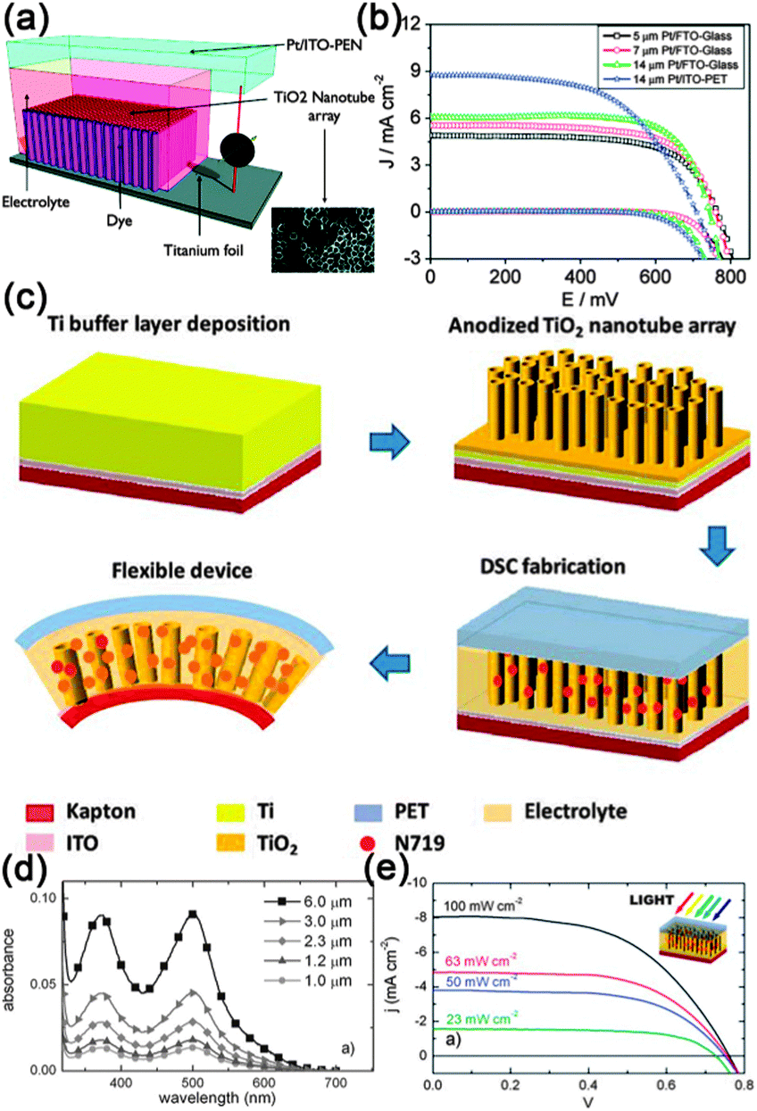 | ||
| Fig. 24 (a) Schematic illustration of the flexible DSSC assembled with the TiO2 nanotube arrays on Ti foil and Pt-coated PEN. (b) Current–voltage characteristics of solar cells based on different TiO2 nanotube lengths using rigid (Pt/FTO-glass) and flexible (Pt/ITO-PEN) substrates. Solid lines were measured under AM 1.5 full sunlight (100 mW cm−2) illumination. The dotted lines were measured in the dark. Reprinted with permission from ref. 240 © 2008, American Chemical Society. (c) Schematic of fabrication of DSCs over flexible Kapton substrates. (d) UV-vis spectrum of N719 dye extracted from a series of TiO2-nanotube arrays with different thicknesses. (e) J–V curves of a DSC under different simulated sunlight intensities. Back-irradiation geometry has been applied, as illustrated in the inset. Reprinted with permission from ref. 244 © 2011, Wiley-VCH. | ||
4.3.1.2 Counter electrodes of flat flexible DSSCs. Pt is usually used as the catalytic materials for tri-iodide reduction and high conductivity. However, as a noble metal, Pt is expensive and exhibits instability in the methoxy propionitrile electrolyte solvents.250 Recently, several kinds of non-Pt materials have been exploited as catalytic materials, such as carbon materials (activated carbon, graphene, carbon nanotubes etc.),251,252 conductive polymers (poly(3,4-ethylenedioxythiophene), PANI etc.),253,254 inorganic materials (CoS, Co9S8, etc.255) and their compounds.256 1D nanostructure based counter electrodes are one of the vital choices to prevent the fragmentation and detachment of materials under tough bending conditions. For example, DSSC with CNT-based coatings on conductive glass exhibited photoelectric conversion efficiency of 10%, which can be attributed to the high electrochemical catalytic activity, excellent conductivity and chemical stability.257 As a promising conductive material for transparent electrodes, CNT can be used as the conductive cover to replace ITO or FTO underlying coating and Pt catalyst at the same time.258–260 The fabrication methods of CNT based flexible counter electrodes include the ink-coating process, growth-detachment-transfer process and the direct usage of free-standing CNT films.259–262 For instance, Chang et al. established a Pt nanoparticle (NP)/CNT hybrid counter electrode on Ti foil by using a stable dispersant consisting of poly(oxyethylene)diamine (POEM) segment and imide linkage functionalities.261 The solution was coated on the foil by the doctor blade technique, followed by annealing at 390 °C to obtain a flexible electrode (Fig. 25a). A conversion efficiency of about 9.04% was obtained (Fig. 25b). The CNTs not only enhanced the surface area and Pt loading but also served as the electrocatalyst. Recently, Malara et al. proposed a free-standing and ultrathin plate by compositing CNTs with polypropylene for the counter electrode,259 as shown in Fig. 25c. The extended etching treatment conditions dramatically benefit the electrochemical properties of the NC/electrolyte as well as the value of the series resistance of the plate (Fig. 25d). Flexible DSSC based on this plate yielded the highest efficiency of 6.67%. In their later work, a much enhanced efficiency of 7.26% was obtained by transferring a vertically aligned carbon nanotube forest onto the CNT–polymer plates, demonstrating a promising implementation of the CNTs as an engineered flexible counter electrode.260
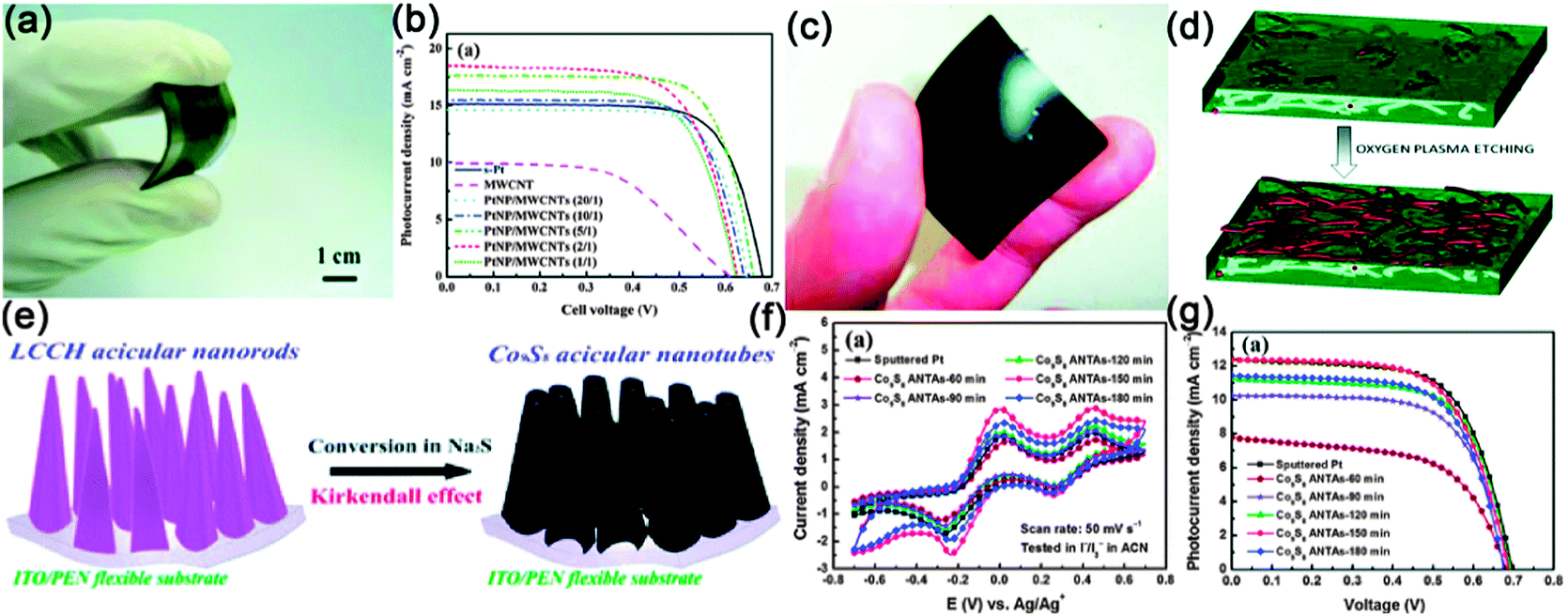 | ||
| Fig. 25 (a) Photograph of a flexible CE with Pt NP/MWCNT. (b) Photocurrent density–voltage curves of the DSSCs using Pt NP/MWCNT CEs with various ratios, measured at 100 mW cm−2 light intensity. s-Pt was also used for comparison. Reprinted with permission from ref. 261 © 2012, The Royal Society of Chemistry. (c) Photograph of a CNT-based monolithic counter electrode and (d) schematic representation of etching treatment effect. Reprinted with permission from ref. 259 © 2011, American Chemical Society. (e) Co9S8 acicular nanotube arrays (ANTAs) are prepared from LCCH acicular nanorod arrays (ANRAs) by soaking in Na2S solution (0.01 M) for 3 h with the help of the Kirkendall effect. (f) CV curves for sputtered Pt and Co9S8 ANTAs CEs prepared with different periods of chemical bath deposition. (g) J–V curves of the DSSCs using sputtered Pt and Co9S8 ANTAs CEs prepared within different periods of CBD. Reprinted with permission from ref. 264 © 2013, The Royal Society of Chemistry. | ||
Metal oxides and sulphides were also used as counter electrodes of DSSCs.263–265 A maximum power conversion efficiency of 7.67% was usually achieved for a cell with CoS nanorod arrays grown on FTO-glass, which is nearly the same as that of a cell with a sputtered Pt counter electrode (7.70%).263 Lately, the authors have fabricated Co9S8 acicular nanorod arrays on a conducting plastic substrate by a two-step approach successfully.264 By chemical bath deposition, layered cobalt carbonate hydroxide acicular nanorod arrays (ANRAs) were fabricated on a conducting plastic substrate, followed by a simple ionic-exchange process in Na2S solution to convert the precursor into Co9S8 nanorod arrays under facile conditions (Fig. 25e). In Fig. 25f, all the CV curves for the Co9S8 ANTAs-60 min, Co9S8 ANTAs-90 min, Co9S8 ANTAs-120 min, Co9S8 ANTAs-150 min and Co9S8 ANTAs-180 min CEs show two pairs of redox peaks, which reveal similar electrochemical behavior to that of the sputtered Pt CE. Finally, a power conversion efficiency of 5.47% was achieved, which was comparable to that of the DSSC using sputtered Pt (5.62%) on the same plastic substrates (Fig. 25g).
The twisted architecture is the most employed one among all the fiber-DSSCs, in which one fiber is coated with photoactive materials and the other one is a counter electrode. The counter electrode (Pt wires, carbon fibers, etc.) is twined on the working electrode with intervals to allow light absorption by the dye molecules. Zou's group has devoted considerable efforts on this kind of fiber DSSCs and achieved a high photo-electric conversion efficiency of 7% by using Pt wire as the counter electrode.132,138 Peng's group reported a further enhanced result by utilizing anodized TiO2 nanotube arrays on a Ti thread as the photoanode and Pt and Ni particle decorated CNT yarns as the counter electrode.277Fig. 26b displays the schematic illustration and SEM image of the photovoltaic wire. This fiber is fairly strong, exhibiting tensile stress of hundreds of megapascals. Decorated by 18.64 wt% and 9.33 wt% of Pt and Ni nanoparticles, respectively, the highest efficiency of 8.03% was obtained. Given the excellent performance, the twisted structure of fiber DSSCs is a promising candidate for practical applications. Chen et al. constructed a series module by five twisted fiber DSSCs, which can successfully drive three commercial light emitting diodes (LEDs) in parallel connection under illumination.269
 | ||
| Fig. 26 (a) Schematic illustration of twisted, parallel and cable-like solar cells. (b) Photovoltaic wire by twisting a TiO2 nanotube-modified titanium wire that serves as the working electrode and an Fe3O4–CNT composite fiber that functions as the counter electrode together. Reprinted with permission from ref. 277 © 2013, Wiley-VCH. (c) Double-metal-wire/PET, double-sided, transparent DSSC device based on Pt–Fe microwires and ZnO NW–Fe microwires. Reprinted with permission from ref. 267 © 2012, Wiley-VCH. (d) Illustration of a coaxial single-wire structure DSSC, consisting of a core Ti wire, dye-grafted TiO2 nanotube arrays, and a flexible, transparent CNT film wrapping around the wire. Reprinted with permission from ref. 273 © 2011, American Chemical Society. (e) Design and principle of a three-dimensional DSSC based on an optic fiber. Reprinted with permission from ref. 279 © 2009, Wiley-VCH. (f) Procedure of all-solid, flexible solar textiles fabricated using DSSC with ZnO NR arrays on SS wires. (g) Photograph of a fabricated flexible woven solar cell. Reprinted with permission from ref. 272 © 2013, Elsevier B.V. (h) A fiber cell being woven with the other CNT fibers into a textile. (i) A fiber cell being woven into a textile composed of aramid fibers. Reprinted with permission from ref. 280 © 2012, American Chemical Society. | ||
Since the twisted structures usually lead to a large part of the working electrode being not covered by the Pt counter electrode and slight wastage of the covered area, parallel arrangement was thus proposed.267 Wang et al. developed a novel methodology for the fabrication of an extended-area, flexible, transparent, double-sided, planar DSSC, formed with metal wire/ZnO-NW arrays as the working electrode and a Pt wire as the counter electrode. Highly ordered, single-crystalline, and high-density ZnO-NW arrays were uniformly deposited onto the Fe microwires. The two metal wires were placed parallel to each other and encapsulated in a poly(ethylene terephthalate) (PET) or polydimethylsiloxane (PDMS) chamber containing the electrolyte (Fig. 26c). The double-wire DSSCs remain stable for a long period of time and can be bent at large angles, up to 107°, reversibly, without any loss of performance.
Cable-like solar cells are also proposed by assembling the active materials on a single substrate wire layer by layer. Zhang et al. developed a cable-like DSSC based on a single Ti wire by wrapping a carbon nanotube film around the Ti wire-supported TiO2 tube arrays as the transparent electrode (Fig. 26d).273 The CNT film ensures full contact with the underlying active layer, as well as uniform illumination along the circumference through the entire DSSC. The single-wire DSSC shows a power conversion efficiency of 1.6% under standard illumination (AM 1.5, 100 mW cm−2). As the cable-like DSSC fiber works on back illumination with the bottom side unilluminated, Wang's group integrated optical fibers and NW arrays as 3D cable-like DSSCs, as shown in Fig. 26e.279 On the lower region of the fiber surface, dye-coated ZnO nanorod arrays are grown on the outer side of the optical fibers, and then assembled with a Pt tube. The key principle is that the light entering from the axial direction inside the fiber experiences multiple internal reflections along the fiber and finally reaches the dye molecules. When the DSSC is illuminated along the fiber axis, an efficiency of 0.44% is achieved, which is much better than the value (0.071%) obtained by vertical illumination.
Based on the successful fabrication of fiber DSSCs, wearable DSSCs can be elaborated via a convenient weaving technology.272,280 For instance, Chae et al. reported a woven DSSC by using ZnO nanorod vertically grown from fiber-type conductive stainless steel (SS) wires as the photoanode and Pt-coated SS wires as the counter electrode.272 As shown in Fig. 26f, all the solid, flexible solar textiles were fabricated by coating dyes and solid-state electrolyte, followed with PET film package. The satin weaving structure was particularly employed due to a larger illumination area as compared to plain and twill weaving structures. The all-solid, flexible properties of the solar textiles fabricated with ZnO NR-based DSSCs are shown in Fig. 26g. The solar textile with 10 × 10 wires exhibited an energy conversion efficiency of 2.57% with a short circuit current density of 20.2 mA cm−2 at 100 mW cm−2 illumination. Chen et al. also reported a woven DSSC by CNT fiber based solar cells.280 A twisted fiber DSSC consists of a CNT fiber and TiO2 coated CNT fiber can be woven into CNT textiles and aramid textiles successfully (Fig. 26h and i), achieving an efficiency of 2.94%.
4.4 Generators
Since it was first proposed by Wang et al. in 2005, the self-powering nanotechnology has attracted much attention in the energy harvesting area. This concept came into existence to serve the interests for driving portable electronics. With the rapid development and wide use of nanotechnology, it is the batteries rather than the devices that finally determine the total size and weight of the system. Moreover, there is a pressing need to design a kind of rather small generator that could provide power for some micro/nano devices or medicine related devices, for example, implantable health monitors and artificial organs etc. Therefore, to meet these technological challenges, it is highly necessary to develop the science and technology closely related to nanogenerators.Wang and his co-workers demonstrated an approach to converting mechanical energy into electric power by using vertical aligned piezoelectric (PZ) NWs,281 and accordingly, designed a series of nanogenerators with sufficient electric output. Here, we only provide one example, as it illustrates the basic principle and technology of nanogenerators.282 In their experiments, vertically aligned ZnO NWs were transferred to a receiving substrate to form horizontally aligned arrays and then parallel-strips-like electrodes were deposited on the horizontal ZnO NW arrays. By connecting a bridge rectifier and a capacitor, a simple self-powered device that could harvest energy from the mechanical bending of the flexible substrate was successfully fabricated. Fig. 27a shows the SEM image of ZnO NW arrays with deposited Au electrodes and the inset shows the photograph of the as-fabricated nanogenerator. Orderly aligned ZnO NWs with a diameter of ∼200 nm served as the active material of the nanogenerators. By an externally applied physical force, the flexible substrate was bent gradually, and correspondingly, the NWs started to deform. The piezoelectric property of the ZnO NW induced a piezoelectric field along the length, which naturally caused a transient charge flow in the external circuit, as shown in Fig. 27b. Repeated bending and releasing of the substrate induced an alternating flow of charges in the external circuit. Time dependent open circuit voltages and short circuit currents are shown in Fig. 27c and d, respectively. From the figures, we could see that an open-circuit voltage as high as 2.03 V and a peak output power density of ∼11 mW cm−3 could be achieved from a single layer NW nanogenerator structure. As shown in the inset of Fig. 27e, an integrated full wave rectifying bridge was connected with a red commercial LED to prove the successful fabrication of the high-output flexible nanogenerators. A total voltage source of 3.7 V and a maximum discharging current of 4.5 mA result in the lighting lasting for 0.1–0.2 s of the LED, as shown in Fig. 27f and g. Through calculations, the effective energy generation efficiency is estimated to be ∼4.6%. Further, by optimizing the density of the NWs on the substrate as well as the use of multilayer integration, many more practical nanogenerators with high open-circuit voltages, high short circuit currents as well as much higher energy generation efficiency are bound to be fabricated.
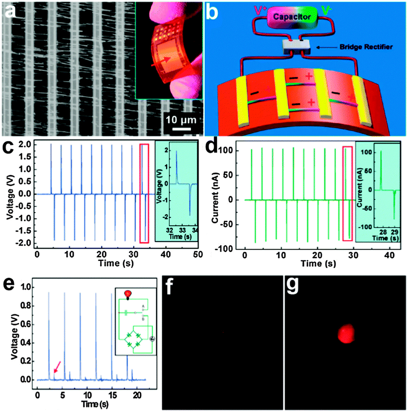 | ||
| Fig. 27 (a) SEM image of active area of the nanogenerator. Inset shows the photograph of an as-fabricated nanogenerator. (b) Demonstration of the operating principle of the nanogenerator when mechanical deformation is induced, where the “±” signs indicate the polarity of the local piezoelectric potential created in the NWs. (c, d) Open circuit voltage and short circuit current measurement of the nanogenerator. The measurement is performed at a strain of 0.1% and strain rate of 5% s−1 under the frequency of 0.33 Hz. Insets are the enlarged view of the single cycle of the signal. (e) Output voltage measured when connected with a full wave rectifying bridge. Here, the arrowhead points out that the signals of the negative signs are reversed. Inset shows the schematic of the charging–discharging circuit. (f, g) Images of the red LED before it was lit up and at the moment when it was lit up by the energy generated from the nanogenerator, respectively. Reprinted with permission from ref. 282 © 2010, American Chemical Society. | ||
5 Integrated devices and systems
The successful fabrication of both NW-based flexible devices and energy conversion/storage sources offer numerous opportunities for the fields of energy system, electronics, automobile, and mechanical equipment. The integration of these semiconductor nanodevices, especially passive devices with power sources, would be of great interest in micro/nano systems' applications. The design and fabrication of high-performance integrated nanopower–nanodevice system, especially flexible systems, present several challenges, for example, impedance matching, electrical/mechanical stability and the improvement of operation efficiency etc. The challenges and limitations of these factors complicate the corresponding improvement. However, there are still a few studies that have focused on the assembly of basic nanodevices into an integrated simple system that can work independently. In this section, the methods and the ultimate performances of several integrated systems will be briefly described.Recently, Wang et al. proposed a flexible self-powered nanosystem, consisting of a multiple lateral-NW-array integrated nanogenerator (VING) and a NW based detector.283 The eventual aim of this design is to be self-driven, that is, the realization of the stable and persistent operation of passive devices without using a battery or external power source. The key to provide a high output voltage and power of the VING is the rational growth of the NWs during the VING fabrication procedure, as the voltage and power produced by a single NW are insufficient for a real device. Fig. 28a shows the experimental procedures designed to fabricate a flexible VING. Briefly, rows of stripe-shaped ZnO pattern with a top and side layer of chromium was first achieved; then, a wet chemical method was used to obtain horizontally grown ZnO NW arrays. Next, gold electrodes were deposited only on the abovementioned chromium layer side, and finally, a layer of soft polymer was spin-coated onto the device to improve the stability and mechanical robustness of the entire structure. Fig. 28b is the SEM image of a single-row VING structure, indicating the ordered alignment of the NWs and the good contacts between the NWs and the electrodes. The final flexible VING was made of 700 rows of NWs on a 125 μm Kapton film. In response to a low-frequency mechanical strain of 0.19% at a straining rate of 2.13% s−1, the average output voltage and the current pulse from the VING were measured to be ∼1.2 V and ∼26 nA, respectively. To demonstrate the ‘self-powered’ performance, the VING was integrated with a single NW-based nanosensor. First, a ZnO NW-based pH sensor was connected with the VING and the voltage across the nanosensor was monitored while changing the degree of acidity versus alkalinity in the target solution (Fig. 28c). An obvious and stable voltage variation corresponding to a local pH change was observed, indicating the high sensitivity of the ‘self-powered’ pH meter. Then, a ZnO NW-based UV sensor was also integrated with the VING (Fig. 28d). When the UV light is turned off, the resistance of the ZnO NW is measured to be ∼10 MΩ, which is comparable to the inner resistance of the VING. Further, the voltage drop across the ZnO NW-based UV sensor was ∼25 mV. Upon UV light illumination, the resistance of the ZnO NW dropped dramatically, and the voltage drop across the ZnO NW-based UV sensor was very small. This clearly indicates that a VING with an output voltage of 20–40 mV can successfully power up various kinds of single-NW-based nanosensors.
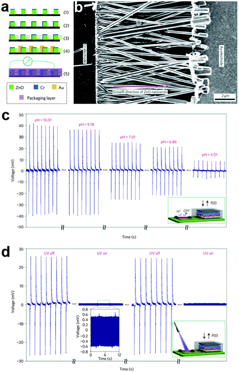 | ||
| Fig. 28 (a) Schematic of the fabrication process of multiple lateral-NW-array integrated nanogenerators. (b) SEM images of a single row of the NWs bonded by metal electrodes. (c) Voltage drop across a single ZnO NW-based pH sensor powered by a VING with an output voltage of ∼40 mV. (d) Voltage drop across a ZnO NW-based UV sensor powered by a VING with an output voltage of ∼25 mV. Insets show the schematics of the NW-based integrated systems. Reprinted with permission from ref. 283 © 2010, Macmillan Publisher Ltd. | ||
Very recently, our group reported a self-powered photodetector, which was driven by a flexible fiber shaped supercapacitor (Fig. 29a and b).284 In this work, uniform Co3O4 NWs (Fig. 29c) were successfully synthesized on different types of metal fibers, namely, nickel and titanium; thereafter, they were fabricated into two kinds of flexible all-solid-state supercapacitors. The as-synthesized Co3O4 NWs were proven to exhibit high capacitance of 2.1 F cm−3 at a current density of 20 mA cm−3 and the final wire shaped all-solid-state supercapacitor was demonstrated to have an impressive capacitive behaviour as well as long cycling performances (as shown in Fig. 29d and e). As discussed above, piezoelectric (PZ) ZnO NWs based nanogenerators could serve as an excellent energy-scavenging unit and could be integrated into a nanosystem to power electrical devices without the need of external batteries. By the same token, Co3O4 NWs based all-solid-state supercapacitors here could also act as power sources. The as-prepared visible light photodetector made from carbon fibers/graphene, which also served as the negative electrode of the flexible all-solid-state asymmetric supercapacitor, was proven to have substantial response to white light irradiation (Fig. 29f). Our primary research work here indicates that the wire shaped flexible supercapacitors can efficiently be used to power electronic and optoelectronic devices, and if the material quality and the device structure could be continually improved, more complicated self-powered devices and systems with minimised sizes and promoted performances will be designed. The harvesting of energy from ambient sources, energy storage/conversion and energy utilization will be more efficient.
 | ||
| Fig. 29 (a, b) Photograph and schematic of the self-powered nanosystem powered by the Co3O4–graphene based fiber-shaped supercapacitor. 1–3 illustrate the different bending states of our flexible asymmetric supercapacitor. (c) SEM images of the as-synthesized Co3O4 NWs grown on nickel fiber used for supercapacitors. (d) CV curves and (e) galvanostatic charge–discharge curves of the fiber-shaped supercapacitor. (f) Current response of the photodetector powered by the supercapacitor. Reprinted with permission from ref. 284 © 2014, Wiley-VCH. | ||
6 Conclusions and outlooks
In this paper, the recent advances in the design and fabrication of NW based flexible devices and their integration have been reviewed. We first present a brief description of different approaches to realize the synthesis of a versatile group of semiconductor NWs and a few methods for the assembly of NWs array. Among the various semiconductors across an expansive area covering from metal oxides to III–V compound, II–VI compound and even multi-metal compounds, many NWs and their combinations such as network, film as well as ordered arrays have shown significant promise for electronic, optoelectronic, photovoltaic, electrochemical and piezoelectric applications. Combining the unique geometric structure of NWs and the superior physical/chemical properties of semiconductors, many kinds of typical nano/micro devices have been designed and fabricated. We show that both individual NW and NW assembled structures offer tempting possibilities in flexible device applications, for example, flexible electrodes and transistors, flexible sensors, flexible display devices, flexible memories and logic gates, as well as flexible energy conversion and storage devices. However, for the NW synthesis and assembly, devices fabrication and system integration processes for economically viable applications require more significant research works.First, even the research in various NWs has witnessed rapid development and substantial achievements; however, certain issues, such as the following, still persist:
(1) Lack of good control over the size of NWs: the difference in properties caused by size heterogeneity is very obvious. A more efficient synthesis method for more precise control of the NWs' size is needed. Owing to the small dimensions and tendency to aggregate, manipulating NWs grown by bottom-up approaches is still challenging. There are two conceptually different types of approaches that can be used to address this problem. The first, a novel 3D printer can be invented to print quality NWs or uniform NW arrays directly. This scheme overcomes the inherent non-uniformity of NWs produced by traditional bottom-up growth process while retaining the advantages of NWs themselves. The second, improved top-down approaches are still attractive when integration and addressability are concerned. As for the manipulating of high density NW arrays, especially for addressability at the single NW level, a new kind of top-down approach has the advantage of being more amenable for large scale integration.
(2) Difficulties in controlling the chemical or physical properties of NWs: NWs with uniform size do not guarantee uniformity in their properties such as electronic transport characteristics. To minimize the NW-to-NW variability is very important but still remains a challenge.
(3) Combinations of different modifying methods over semiconductor NWs need to be systematically studied. Doping, surface modification, organic–inorganic hybrid, and the formation of multiple compounds or heterojunctions have been extensively studied for more than a decade. Still, a successful modification method would require the consideration of numerous factors such as surface states, defects, traps, catalysts-induced contamination, orientation and polarization of NWs. It seems a bit difficult to select an efficient way to modify the as-prepared NWs based on their ultimate use. Therefore, establishing an effective method for determining the modification process is fairly critical.
(4) The yield of NWs with high quality for scalable device fabrication and integration is significantly insufficient.
(5) In particular, each current NW assembly technique has its advantages and weaknesses, and it creates certain difficulties in printing NWs precisely on flexible substrates. The existing NW assembly techniques are also inefficient and incur high time costs. More appropriate NW assembly techniques need to be improvised and different types of assembly methods should be combined to yield high quality NW arrays.
Second, there is an obvious challenge in optimizing the configuration and fabrication process of flexible devices. By taking the advantages of 1-D geometric features and excellent physical/chemical properties of NWs, a group of nanodevices have been created. However, most of them are just the basic unit that could only be used for NWs' properties measurement. In other words, most existing nanodevices are inappropriate for practical applications. For example, NW based photodetectors are still at an early stage. Most current NW photodetectors have much lower performance in efficiency and bandwidth when compared with their classical counterparts,285 and the device-to-device variability of the performance has largely limited their development and applications. Besides, measurement theory and methods related to device properties should be found to the needs of specific and novel devices, for example, some sensors work in a harsh environment286 or under variable conditions. New measurement and evaluation methods then should be formulated. Although the optimization of the electronic/optoelectronic performance of many flexible devices is still under way, we are of the view that offering a few new, entry-level products provides a new impetus for exploring this largely uncharted territory. Roll-up portable displays, sensory skins and electronically steerable antenna arrays for wireless communication, in our opinion, will be in considerable demand during the coming years. Furthermore, commercializing some of the important applications will undoubtedly stir up more interest in this area.
Third, flexibility is one of the highlights of several devices and much more importance should be continuously attached to it. Flexible display devices have been a part of several promising ventures. If an efficient way can be found to ensure both high performance and outstanding flexibility for nanodevices, much more functional industrial products based on 1-D nanostructures will be designed.
At last, appropriate combinations of two or more as-fabricated NW devices will lead to some particularly exciting achievements. Combining appropriate electronic devices with energy units into a fully flexible system, in particular, is of special significance. Owing to the urgent demand of next-generation consumer electronics and with the rapid development of nanotechnology, integrated 1-D NW devices and systems are the most promising field to be realized in the near future. Besides, miniaturization, high integration and portability are the necessary requirements of future electronics. For example, nanoscale sensors can be equipped with tiny self-powered elements and microwave communication components to serve as body-implantable sensing networks. Considering these, many start-ups want scientists to engage in the applied research of fully flexible systems, rather than fundamental research of individual components. Fundamental breakthroughs, although important, should not dominate our research results list. The future of flexible inorganic NW electronics, in our opinion, will be largely dependent on how effectively we can balance the functionality, stability as well as the cost of NW-based flexible systems. We believe cooperation between entrepreneurs and scientists will certainly accelerate our research in this area. Assembling existing components into functional and smart systems, increasing their availability and reliability and then introducing them to the market is basically the only way to realize the commercial and industrial applications of flexible electronics.
Acknowledgements
This work was supported by the National Natural Science Foundation (61377033 and 91123008).Notes and references
- B. K. Kim, S.-K. Lee, M. S. Kang, J.-H. Ahn and J. H. Cho, ACS Nano, 2012, 6, 8646–8651 CrossRef CAS PubMed.
- D. Grimm, C. C. B. Bufon, C. Deneke, P. Atkinson, D. J. Thurmer, F. Schäffel, S. Gorantla, A. Bachmatiuk and O. G. Schmidt, Nano Lett., 2013, 13, 213–218 CrossRef CAS PubMed.
- L. Y. Yuan, J. J. Dai, X. H. Fan, T. Song, Y. T. Tao, K. Wang, Z. Xu, J. Zhang, X. D. Bai, P. X. Lu, J. Chen, J. Zhou and Z. L. Wang, ACS Nano, 2011, 5, 4007–4013 CrossRef CAS PubMed.
- Y. Sun and J. A. Rogers, Adv. Mater., 2007, 15, 1897–1916 CrossRef.
- R. T. Hamers, Nature, 2001, 412, 489–490 CrossRef CAS PubMed.
- P.-C. Chen, G. Z. Shen, H. Chen, Y. G. Ha, C. Wu, S. Sukcharoenchoke, Y. Fu, J. Liu, A. Facchetti, T. J. Marks, M. E. Thompson and C. W. Zhou, ACS Nano, 2009, 3, 3383–3390 CrossRef CAS PubMed.
- D. R. Cairns and G. P. Crawford, Proc. IEEE, 2005, 93, 1451–1458 CrossRef CAS.
- J. Yoon, A. J. Baca, S. Park, P. Elvikis, J. B. Geddes, L. F. Li, R. H. Kim, J. L. Xiao, S. D. Wang, T. H. Kim, M. J. Motala, B. Y. Ahn, E. B. Duoss, J. A. Lewis, R. G. Nuzzo, P. M. Ferreira, Y. G. Huang, A. Rockett and J. A. Rogers, Nat. Mater., 2008, 7, 907–915 CrossRef CAS PubMed.
- C. Y. Chang, Y. J. Cheng, S. H. Hung, J. S. Wu, W. S. Kao, C. H. Lee and C. S. Hsu, Adv. Mater., 2012, 24, 549–553 CrossRef CAS PubMed.
- W. T. S. Huck, Nat. Mater., 2005, 4, 271–272 CrossRef CAS.
- K. Efimenko, M. Rackaitis, E. Manias, A. Vaziri, L. Mahadevan and J. Genzer, Nat. Mater., 2005, 4, 293–297 CrossRef CAS PubMed.
- S. Ju, A. Facchetti, Y. Xuan, J. Liu, F. Ishikawa, P. D. Ye, C. W. Zhou, T. J. Marks and D. B. Janes, Nat. Nanotechnol., 2007, 2, 378–384 CrossRef CAS PubMed.
- K. H. Cherenack, A. Z. Kattamis, B. Hekmatshoar, J. C. Sturm and S. Wagner, IEEE Electron Device Lett., 2007, 28, 1004–1006 CrossRef CAS.
- R. J. Hamers, Nature, 2001, 412, 489–490 CrossRef CAS PubMed.
- S. R. Forrest, Nature, 2004, 428, 911–918 CrossRef CAS PubMed.
- G. H. Gelinck, H. E. A. Huitema, E. V. Veenendaal, E. Cantatore, L. Schrijnemakers, J. B. P. H. V. D. Putten, T. C. T. Geuns, M. Beenhakkers, J. B. Giesbers, B. H. Huisman, E. J. Meijer, E. M. Benito, F. J. Touwslager, A. W. Marsman, B. J. E. V. Rens and D. M. Leeuw, Nat. Mater., 2004, 3, 106–110 CrossRef CAS PubMed.
- T. Someya, Y. Kato, T. Sekitani, S. Iba, Y. Noguchi, Y. Murase, H. Kawaguchi and T. Sakurai, Proc. Natl. Acad. Sci. U. S. A., 2005, 102, 12321–12325 CrossRef CAS PubMed.
- G. Eda, G. Fanchini and M. Chhowalla, Nat. Nanotechnol., 2008, 3, 270–274 CrossRef CAS PubMed.
- J. H. Burroughes, D. D. C. Bradley, A. R. Brown, R. N. Marks, K. Mackay, R. H. Friend, P. L. Burns and A. B. Holmes, Nature, 1990, 347, 539–541 CrossRef CAS.
- S. Lamansky, P. Djurovich, D. Murphy, F. A. Razzaq, H. E. Lee, C. Adachi, P. E. Burrows, S. R. Forrest and M. E. Thompson, J. Am. Chem. Soc., 2001, 123, 4304–4312 CrossRef CAS PubMed.
- S. Reineke, F. Lindner, G. Schwartz, N. Seidler, K. Walzer, B. Lüssem and K. Leo, Nature, 2009, 459, 234–238 CrossRef CAS PubMed.
- S. Soeren, D. V. Stijn, M. Kris, L. Martijin, G. Jan and H. Paul, J. Appl. Phys., 2006, 99, 114519 CrossRef PubMed.
- R. Robert, M. Siddharth, O. Viorel, W. Robert, G. Michelle, D. Klaus, S. Oleg and D. Ananth, Appl. Phys. Lett., 2006, 88, 123502 CrossRef PubMed.
- L. E. Kreno, K. Leong, O. K. Farha, M. Allendorf, R. P. V. Duyne and J. T. Hupp, Chem. Rev., 2012, 112, 1105–1125 CrossRef CAS PubMed.
- C. B. Black, B. Andrioletti, A. C. Try, C. Ruiperez and J. L. Sessler, J. Am. Chem. Soc., 1999, 121, 10438–10439 CrossRef CAS.
- J. Li, Y. J. Lu, Q. Ye, M. Cinke, J. Han and M. Meyyappan, Nano Lett., 2003, 3, 929–933 CrossRef CAS.
- A. Dodabalapur, L. Torsi and H. E. Katz, Science, 1995, 268, 270 CAS.
- K. Nomura, H. Ohta, K. Ueda, T. Kamiya, M. Hirano and H. Hosono, Science, 2003, 300, 1269 CrossRef CAS PubMed.
- K. Nomura, H. Ohta, A. Takagi, T. Kamiya, M. Hirano and H. Hosono, Nature, 2004, 432, 488 CrossRef CAS PubMed.
- Y. Yamashita, Sci. Technol. Adv. Mater., 2009, 10, 024313 CrossRef.
- S. Y. Park, B. J. Kim, K. Kim, M. S. Kang, K. H. Lim, T. I. Lee, J. M. Myoung, H. K. Baik, J. H. Cho and Y. S. Kim, Adv. Mater., 2012, 24, 834 CrossRef CAS PubMed.
- N. A. Azarova, J. W. Owen, C. A. McLellan, M. A. Grimminger, E. K. Chapman, J. E. Anthony and O. D. Jurchescu, Org. Electron., 2010, 11, 1960 CrossRef CAS PubMed.
- J. Li, C. Papadopoulos, J. M. Xu and M. Moskovits, Appl. Phys. Lett., 1999, 75, 367 CrossRef CAS PubMed.
- S. Cui, H. B. Liu, L. B. Gan, Y. L. Li and D. B. Zhu, Adv. Mater., 2008, 20, 2918–2925 CrossRef CAS.
- C. A. Wang, K. M. Ryu, A. Badmaev, J. L. Zhang and C. W. Zhou, ACS Nano, 2011, 5, 1147 CrossRef CAS PubMed.
- C. Wang, A. Badmaev, A. Jooyaie, M. Q. Bao, K. L. Wang, K. Galatsis and C. W. Zhou, ACS Nano, 2011, 5, 4169 CrossRef CAS PubMed.
- G. Z. Shen, B. Liang, X. F. Wang, P. C. Chen and C. W. Zhou, ACS Nano, 2011, 5, 2155 CrossRef CAS PubMed.
- Z. Liu, H. T. Huang, B. Liang, X. F. Wang, Z. R. Wang, D. Chen and G. Z. Shen, Opt. Express, 2012, 20, 2982–2991 CrossRef CAS PubMed.
- D. M. Sun, M. Y. Timmermans, Y. Tian, A. G. Nasibulin, E. I. Kauppinen, S. Kishimoto, T. Mizutani and Y. Ohno, Nat. Nanotechnol., 2011, 6, 156–161 CrossRef CAS PubMed.
- C. Kocabas, H. S. Kim, T. Banks, J. A. Rogers, A. A. Pesetski, J. E. Baumgardner, S. V. Krishnaswamy and H. Zhang, Proc. Natl. Acad. Sci. U. S. A., 2008, 105, 1045–1049 CrossRef PubMed.
- J. Appenzeller, Proc. IEEE, 2008, 96, 201–211 CrossRef CAS.
- M. Rinkiö, A. Johansson, G. S. Paraoanu and P. Törmä, Nano Lett., 2009, 9, 643–647 CrossRef PubMed.
- A. B. Kaul, E. W. Wong, L. Epp and B. D. Hunt, Nano Lett., 2006, 6, 942–947 CrossRef CAS PubMed.
- T. Durkop, S. A. Getty, E. Cobas and M. S. Fuhrer, Nano Lett., 2004, 4, 35–39 CrossRef.
- E. T. Thostenson, Z. F. Ren and T. W. Chou, Compos. Sci. Technol., 2001, 61, 1899–1912 CrossRef CAS.
- T. Takenobu, T. Takahashi, T. Kanbara, K. Tsukagoshi, Y. Aoyagi and Y. Iwasa, Appl. Phys. Lett., 2006, 88, 33511–33513 CrossRef PubMed.
- Q. Cao, S. H. Hur, Z. T. Zhu, Y. Sun, C. Wang, M. A. Meitl, M. Shim and J. A. Rogers, Adv. Mater., 2006, 18, 304–309 CrossRef CAS.
- E. Artukovic, M. Kaempgen, D. S. Hecht, S. Roth and G. Gruner, Nano Lett., 2005, 5, 757–760 CrossRef CAS PubMed.
- F. N. Ishikawa, H. K. Chang, K. Ryu, P. C. Chen, A. Badmaev, L. G. D. Arco, G. Z. Shen and C. W. Zhou, ACS Nano, 2009, 3, 73–79 CrossRef CAS PubMed.
- Y. Che, C. Wang, J. Liu, B. L. Liu, X. Lin, J. Parker, C. Beasley, H. S. P. Wong and C. W. Zhou, ACS Nano, 2012, 6, 7454–7462 CrossRef CAS PubMed.
- E. Stern, J. F. Klemic, D. A. Routenberg, P. N. Wyrembak, D. B. T. Evans, A. D. Hamilton, D. A. Lavan, T. M. Fahmy and M. A. Reed, Nature, 2007, 445, 519–522 CrossRef CAS PubMed.
- Z. Liu, B. Liang, G. Chen, G. Yu, Z. Xie, L. N. Gao, D. Chen and G. Z. Shen, J. Mater. Chem. C, 2013, 1, 131–137 RSC.
- G. D. Mahan, R. Gupta, Q. Xiong, C. K. Adu and P. C. Eklund, Phys. Rev. B: Condens. Matter Mater. Phys., 2003, 68, 073402 CrossRef.
- M. S. Gudiksen, L. J. Lauhon, J. F. Wang, D. C. Smith and C. M. Lieber, Nature, 2002, 415, 617–620 CrossRef CAS PubMed.
- R. Q. Zhang, Y. Lifshitz and S. T. Lee, Adv. Mater., 2003, 15, 635–640 CrossRef CAS.
- Z. Liu, G. Chen, B. Liang, G. Yu, H. T. Huang, D. Chen and G. Z. Shen, Opt. Express, 2013, 21, 7799–7810 CrossRef CAS PubMed.
- A. I. Hochbaum and P. D. Yang, Chem. Rev., 2010, 110, 527–546 CrossRef CAS PubMed.
- P. D. Yang, R. X. Yan and M. Fardy, Nano Lett., 2010, 10, 1529–1536 CrossRef CAS PubMed.
- H. T. Huang, B. Liang, Z. Liu, X. F. Wang, D. Chen and G. Z. Shen, J. Mater. Chem., 2012, 22, 13428–13445 RSC.
- M. Law, J. Goldberger and P. D. Yang, Annu. Rev. Mater. Res., 2004, 34, 83–122 CrossRef CAS.
- B. M. Wen, J. E. Sader and J. J. Boland, Phys. Rev. Lett., 2008, 101, 175502 CrossRef.
- D.-H. Kim, N. S. Lu, R. Ghaffari and J. A. Rogers, NPG Asia Mater., 2012, 4, 15 CrossRef.
- X. F. Wang, B. Liu, Q. F. Wang, W. F. Song, X. J. Hou, D. Chen, Y.-B. Chen and G. Z. Shen, Adv. Mater., 2013, 25, 1479–1486 CrossRef CAS PubMed.
- B. Liu, X. F. Wang, H. T. Chen, Z. R. Wang, D. Chen, Y.-B. Cheng, C. W. Zhou and G. Z. Shen, Sci. Rep., 2013, 3, 1622 Search PubMed.
- X. Wang, J. Zhuang, Q. Peng and Y. D. Li, Nature, 2005, 437, 121–124 CrossRef CAS PubMed.
- Y. Cui, L. J. Lauhon, M. S. Gudiksen, J. F. Wang and C. M. Lieber, Appl. Phys. Lett., 2001, 78, 2214 CrossRef CAS PubMed.
- C. Wang, Y. J. Hu, C. M. Lieber and S. S. Heng, J. Am. Chem. Soc., 2008, 130, 8902–8903 CrossRef CAS PubMed.
- J. M. Cai, P. Ruffieux, R. Jaafar, M. Bieri, T. Braun, S. Blankenburg, M. Muoth, A. P. Seitsonen, M. Saleh, X. L. Feng, K. Müllen and R. Fasel, Nature, 2010, 466, 470–473 CrossRef CAS PubMed.
- G. B. Rossi, G. Beaucage, T. D. Dang and R. A. Vaia, Nano Lett., 2002, 2, 319–323 CrossRef CAS.
- J. D. Holmes, K. P. Johnston, R. C. Doty and B. A. Korgel, Science, 2000, 287, 1471–1473 CrossRef CAS.
- Y. G. Sun, B. Gates, B. Mayer and Y. N. Xia, Nano Lett., 2002, 2, 165–168 CrossRef CAS.
- B. Weintraub, Z. Z. Zhou, Y. H. Li and Y. L. Deng, Nanoscale, 2010, 2, 1573–1587 RSC.
- A. P. Alivisatos, J. Phys. Chem., 1996, 100, 13226–13239 CrossRef CAS.
- J. Xu, Y. G. Zhu, H. T. Huang, Z. Xie, D. Chen and G. Z. Shen, CrystEngComm, 2011, 13, 2629–2635 RSC.
- A. Birkel, N. Loges, E. Mugnaioli, R. Branscheid, D. Koll, S. Frank, M. Panthöfer and W. Tremel, Langmuir, 2010, 26, 3590–3595 CrossRef CAS PubMed.
- X. M. Sun and Y. D. Li, Adv. Mater., 2005, 17, 2626–2630 CrossRef CAS.
- Z. P. Zhu, Y. Yang, J. B. Liang, Z. K. Hu, S. Li, S. Peng and Y. T. Qian, J. Phys. Chem. B, 2003, 107, 12658–12661 CrossRef.
- T. Y. Zhai, X. S. Fang, M. Y. Liao, X. J. Liu, H. B. Zeng, B. Yoshio and D. Golberg, Sensors, 2009, 9, 6504–6529 CrossRef CAS PubMed.
- G. Z. Shen, J. Xu, X. F. Wang, H. T. Huang and D. Chen, Adv. Mater., 2011, 23, 771 CrossRef CAS PubMed.
- G. Chen, Z. Liu, B. Liang, G. Yu, Z. Xie, H. T. Huang, B. Liu, X. F. Wang, D. Chen and G. Z. Shen, Adv. Funct. Mater., 2013, 21, 2681 CrossRef.
- D. Routkevitch, T. Bibioni, M. Moskovits and J. M. Xu, J. Phys. Chem., 1996, 100, 14037–14047 CrossRef CAS.
- L. L. Wang, J. N. Deng, Z. Lou and T. Zhang, J. Mater. Chem. A, 2014, 2, 10022–10028 CAS.
- L. Y. Zhang, J. Feng and D. S. Xue, Mater. Lett., 2007, 61, 1363 CrossRef CAS PubMed.
- D. S. Xue, L. Y. Zhang, A. B. Gui and X. F. Xu, Appl. Phys. A: Mater. Sci. Process., 2005, 80, 439 CrossRef CAS.
- S. M. Roper, H. S. Davis, S. A. Norris, A. A. Golovin, P. W. Voorhees and M. Weiss, J. Appl. Phys., 2007, 102, 034304 CrossRef PubMed.
- K. C. Grabar, R. G. Freeman, M. B. Hommer and M. J. Natan, Anal. Chem., 1995, 67, 735–743 CrossRef CAS.
- R. S. Wagner, W. C. Ellis, K. A. Jackson and S. M. Arnold, J. Appl. Phys., 1964, 35, 2993 CrossRef CAS PubMed.
- Y. Y. Wu and P. D. Yang, J. Am. Chem. Soc., 2001, 123, 3165–3166 CrossRef CAS.
- K.-K. Lew, L. Pan, E. C. Dickey and J. M. Redwing, Adv. Mater., 2003, 15, 2073–2076 CrossRef CAS.
- Y. Ding, P. X. Gao and Z. L. Wang, J. Am. Chem. Soc., 2004, 126, 2066–2072 CrossRef CAS PubMed.
- Y. Li, Y. Bando and D. Golberg, Adv. Mater., 2003, 15, 581–585 CrossRef CAS.
- Q. Wan, M. Wei, D. Zhi, J. L. MacManus-Driscoll and M. G. Blamire, Adv. Mater., 2006, 18, 234 CrossRef CAS.
- Q. Wan, P. Feng and T. H. Wang, Appl. Phys. Lett., 2006, 89, 123102 CrossRef PubMed.
- J. H. He, J. H. Hsu, C. W. Wang, H. N. Lin, L. J. Chen and Z. L. Wang, J. Phys. Chem. B, 2006, 110, 50–53 CrossRef CAS PubMed.
- L. E. Greene, M. Law, D. H. Tan, M. Montano, J. Goldberger, G. Somorijai and P. D. Yang, Nano Lett., 2005, 5, 1231–1236 CrossRef CAS.
- Z. Ying, Q. Wan, Z. T. Song and S. L. Feng, Mater. Lett., 2005, 59, 1670–1672 CrossRef CAS PubMed.
- N. Sköld, L. S. Karlsson, M. W. Larsson, M.-E. Pistol, W. Seifert, J. Trägårdh and L. Samuelson, Nano Lett., 2005, 5, 1943–1947 CrossRef PubMed.
- A. Umar, S. H. Kim, Y.-S. Lee, K. S. Nahm and Y. B. Hahn, J. Cryst. Growth, 2005, 282, 131–136 CrossRef CAS PubMed.
- S. H. Sun, G. W. Meng, Y. W. Wang, T. Gao, M. G. Zhang, Y. T. Tian, X. S. Peng and L. D. Zhang, Appl. Phys. A: Mater. Sci. Process., 2003, 76, 287–289 CrossRef CAS PubMed.
- X. S. Peng, G. W. Meng, J. Zhang, X. F. Wang, Y. W. Wang, C. Z. Wang and L. D. Zhang, J. Mater. Chem., 2002, 12, 1602–1605 RSC.
- D. H. Fan, J. Cryst. Growth, 2009, 311, 2300–2304 CrossRef CAS PubMed.
- L. S. Wang, X. Z. Zhang, S. Q. Zhao, G. Y. Zhou, Y. L. Zhou and J. J. Qi, Appl. Phys. Lett., 2005, 86, 024108 CrossRef PubMed.
- Y. Huang, X. F. Duan, Q. Q. Wei and C. M. Lieber, Science, 2001, 291, 630–633 CrossRef CAS PubMed.
- G. H. Yu, A. Y. Cao and C. M. Lieber, Nat. Nanotechnol., 2007, 2, 372–377 CrossRef CAS PubMed.
- C. M. Hangarter and N. V. Myung, Chem. Mater., 2005, 17, 1320–1324 CrossRef CAS.
- E. M. Freer, O. Grachev, X. F. Duan, S. Martin and D. P. Stumbo, Nat. Nanotechnol., 2010, 5, 525–530 CrossRef CAS PubMed.
- Z. Y. Fan, J. C. Ho, Z. A. Jacobson, R. Yerushalmi, R. L. Alley, H. Razavi and A. Javey, Nano Lett., 2008, 8, 20–25 CrossRef CAS PubMed.
- A. C. Ford, J. C. Ho, Z. Y. Fan, O. Ergen, V. Altoe, S. Aloni, H. Razavi and A. Javey, Nano Res., 2008, 1, 32–39 CrossRef CAS.
- R. Yerushalmi, Z. A. Jacobson, J. C. Ho, Z. Y. Fan and A. Javey, Appl. Phys. Lett., 2007, 91, 203104 CrossRef PubMed.
- S.-Y. Min, T.-S. Kim, B.-J. Kim, H. Cho, Y.-Y. Noh, H. Yang, J. H. Cho and T.-W. Lee, Nat. Commun., 2013, 4, 1773 CrossRef PubMed.
- H. Cho, S.-Y. Min and T.-W. Lee, Macromol. Mater. Eng., 2013, 298, 475–486 CrossRef CAS.
- D. Li and Y. Xia, Adv. Mater., 2004, 16, 1151–1170 CrossRef CAS.
- A. L. Briseno, S. C. B. Mannsfeld, S. A. Jenekhe, Z. N. Bao and Y. N. Xia, Mater. Today, 2008, 11, 38–47 CrossRef CAS.
- N. L. Liu, Y. Zhou, N. Ai, C. Luo, J. B. Peng, J. Wang, J. Pei and Y. Cao, Langmuir, 2011, 27, 14710–14715 CrossRef CAS PubMed.
- X. J. Zhang, J. S. Jie, W. F. Zhang, C. Y. Zhang, L. B. Luo, Z. B. He, X. H. Zhang, W. J. Zhang, C. Lee and S. T. Lee, Adv. Mater., 2008, 20, 2427–2432 CrossRef CAS.
- Y. P. Zhang, X. D. Wang, Y. M. Wu, J. S. Jie, X. W. Zhang, Y. L. Xing, H. H. Wu, B. Zou, X. J. Zhang and X. H. Zhang, J. Mater. Chem., 2012, 22, 14357–14362 RSC.
- L. Persano, C. Degdeviren, Y. W. Su, Y. H. Zhang, S. Girardo, D. Pisignano, Y. G. Huang and J. A. Rogers, Nat. Commun., 2013, 4, 1633 CrossRef PubMed.
- A. R. Madaria, A. Kumar, F. N. Ishikawa and C. W. Zhou, Nano Res., 2010, 3, 564–573 CrossRef CAS PubMed.
- L. B. Hu, H. S. Kim, J.-Y. Lee, P. Peumans and Y. Cui, ACS Nano, 2010, 5, 2955–2963 CrossRef PubMed.
- A. R. Rathmell and B. J. Wiley, Adv. Mater., 2011, 23, 4798–4803 CrossRef CAS PubMed.
- T. Takahashi, K. Takei, E. Adabi, Z. Y. Fan, A. M. Niknejad and A. Javey, ACS Nano, 2010, 10, 5855–5860 CrossRef PubMed.
- M. C. Mcalpine, H. Ahmad, D. W. Wang and J. R. Heath, Nat. Mater., 2007, 6, 379–384 CrossRef CAS PubMed.
- D. K. Kim, Y. M. Lai, T. R. Vemulkar and C. R. Kagan, ACS Nano, 2011, 12, 10074–10083 CrossRef PubMed.
- D. V. Talapin and C. B. Murray, Science, 2005, 310, 86–89 CrossRef CAS PubMed.
- F. Patolsky and C. M. Lieber, Mater. Today, 2005, 8, 20–28 CrossRef CAS.
- H. Kind, H. Q. Yan, B. Messer, M. Law and P. D. Yang, Adv. Mater., 2002, 14, 158–160 CrossRef CAS.
- C.-H. Lin, T.-T. Chen and Y.-F. Chen, Opt. Express, 2008, 16, 16916–16922 CrossRef CAS.
- D. Zhang, C. Li, S. Han, X. Liu, T. Tang, W. Jin and C. W. Zhou, Appl. Phys. A: Mater. Sci. Process., 2003, 77, 163–166 CrossRef CAS PubMed.
- L. Wang, M. Lu, P. Lv, J. S. Jie, T. X. Yan, Y. Q. Yu, C. Y. Wu, Y. Zhang, C. Xie, P. Jiang, Z. Wang and Z. H. Hu, Sci. Adv. Mater., 2012, 4, 332–336 CrossRef CAS PubMed.
- T. Y. Zhai, M. F. Ye, L. Li, X. S. Fang, M. Y. Liao, Y. F. Li, Y. Koide, Y. Bando and D. Golberg, Adv. Mater., 2010, 22, 4530–4533 CrossRef CAS PubMed.
- Z. T. You, X. S. Fang, M. Y. Liao, X. J. Xu, L. Li, B. D. Liu, Y. Koide, Y. Ma, J. N. Yao, Y. Bando and D. Golberg, ACS Nano, 2010, 4, 1596–1602 CrossRef PubMed.
- Z. X. Wang, M. Safdar, C. Jiang and J. He, Nano Lett., 2012, 12, 4715–4721 CrossRef CAS PubMed.
- J. Svensson, N. Anttu, N. Vainorius, B. M. Borg and L. E. Wernersson, Nano Lett., 2013, 13, 1380–1385 CAS.
- C. Y. Yan, N. D. Singh and P. S. Lee, Appl. Phys. Lett., 2010, 96, 053108 CrossRef PubMed.
- C. Y. Yan and P. S. Lee, Sci. Adv. Mater., 2012, 4, 241–253 CrossRef CAS PubMed.
- S. Bai, W. W. Wu, Y. Qin, N. Y. Cui, D. J. Bayerl and X. D. Wang, Adv. Funct. Mater., 2011, 21, 4464–4469 CrossRef CAS.
- G. Chen, Z. Liu, B. Liang, G. Yu, Z. Xie, H. T Huang, B. Liu, X. F. Wang, D. Chen, M. Q. Zhu and G. Z. Shen, Adv. Funct. Mater., 2013, 23, 2681–2690 CrossRef CAS.
- R. R. He and P. D. Yang, Nat. Nanotechnol., 2006, 1, 42–46 CrossRef CAS PubMed.
- J. Zhou, Y. D. Gu, P. Fei, W. J. Mai, Y. F. Gao, R. S. Yang, G. Bao and Z. L. Wang, Nano Lett., 2008, 8, 3973–3977 CrossRef CAS PubMed.
- S. C. B. Mannsfeld, B. C.-K. Tee, C.-K. Tee, R. M. Stoltenberg, C. V. H.-H. Chen, S. Barman, B. V. O. Muir, A. N. Sokolov, C. Reese and Z. N. Bao, Nat. Mater., 2010, 9, 859–864 CrossRef CAS PubMed.
- K. Takei, T. Takahashi, J. C. Ho, H. Ko, A. G. Gillies, P. W. Leu, R. S. Fearing and A. Javey, Nat. Mater., 2010, 9, 821–826 CrossRef CAS PubMed.
- C. Wang, D. Hwang, Z. B. Zhu, K. Takei, J. Park, T. Chen, B. W. Ma and A. Javey, Nat. Mater., 2013, 12, 899–904 CrossRef CAS PubMed.
- M. C. McAlpine, R. S. Friedman, S. Jin, K.-H. Lin, W. U. Wang and C. M. Lieber, Nano Lett., 2003, 3, 1531–1535 CrossRef CAS.
- A. Nadarajah, R. C. Word, J. Meiss and R. Könenkamp, Nano Lett., 2008, 8, 534–537 CrossRef CAS PubMed.
- A. Javey, S. W. Nam, R. S. Friedman, H. Yan and C. M. Lieber, Nano Lett., 2007, 7, 773–777 CrossRef CAS PubMed.
- Y. G. Sun, H.-S. Kim, E. Menard, S. Kim, I. Adesida and J. A. Rogers, Small, 2006, 2(11), 1330–1334 CrossRef CAS PubMed.
- Q. Cao, H.-S. Kim, N. Pimparkar, J. P. Kulkarni, C. Wang, M. Shim, K. Roy, M. A. Alam and J. A. Rogers, Nature, 2008, 454, 495–500 CrossRef CAS PubMed.
- M. Armand and J. M. Tarascon, Nature, 2008, 451, 652–657 CrossRef CAS PubMed.
- H. Wu and Y. Cui, Nano Today, 2012, 7, 414–429 CrossRef CAS PubMed.
- A. S. Arico, P. Bruce, B. Scrosati, J.-M. Tarascon and W. van Schalkwijk, Nat. Mater., 2005, 4, 366–377 CrossRef CAS PubMed.
- S. Iijima, Nature, 1991, 354, 56–58 CrossRef CAS.
- B. Gao, C. Bower, J. D. Lorentzen, L. Fleming, A. Kleinhammes, X. P. Tang, L. E. McNeil, Y. Wu and O. Zhou, Chem. Phys. Lett., 2000, 327, 69–75 CrossRef CAS.
- S. W. Lee, N. Yabuuchi, B. M. Gallant, S. Chen, B.-S. Kim, P. T. Hammond and Y. Shao-Horn, Nat. Nanotechnol., 2010, 5, 531–537 CrossRef CAS PubMed.
- S. Y. Chew, S. H. Ng, J. Wang, P. Novák, F. Krumeich, S. L. Chou, J. Chen and H. K. Liu, Carbon, 2009, 47, 2976–2983 CrossRef CAS PubMed.
- J. Chen, A. I. Minett, Y. Liu, C. Lynam, P. Sherrell, C. Wang and G. G. Wallace, Adv. Mater., 2008, 20, 566–570 CrossRef CAS.
- B. J. Landi, M. J. Ganter, C. M. Schauerman, C. D. Cress and R. P. Raffaelle, J. Mater. Chem., 2008, 112, 7509–7515 CAS.
- X. Li, J. Yang, Y. Hu, J. Wang, Y. Li, M. Cai, R. Li and X. Sun, J. Mater. Chem., 2012, 22, 18847–18853 RSC.
- L. Hu, H. Wu, F. La Mantia, Y. Yang and Y. Cui, ACS Nano, 2010, 4, 5843–5848 CrossRef CAS PubMed.
- K. Wang, S. Luo, Y. Wu, X. F. He, F. Zhao, J. P. Wang, K. L. Jiang and S. S. Fan, Adv. Funct. Mater., 2013, 23, 846–853 CrossRef CAS.
- L. Hu, F. La Mantia, H. Wu, X. Xie, J. McDonough, M. Pasta and Y. Cui, Adv. Energy Mater., 2011, 1, 1012–1017 CrossRef CAS.
- V. L. Pushparaj, M. M. Shaijumon, A. Kumar, S. Murugesan, L. Ci, R. Vajtai, R. J. Linhardt, O. Nalamasu and P. M. Ajayan, Proc. Natl. Acad. Sci. U. S. A., 2007, 104, 13574–13577 CrossRef CAS PubMed.
- L. Hu and Y. Cui, Energy Environ. Sci., 2012, 5, 6423–6435 Search PubMed.
- L. Hu, J. W. Choi, Y. Yang, S. Jeong, F. La Mantia, L.-F. Cui and Y. Cui, Proc. Natl. Acad. Sci. U. S. A., 2009, 106, 21490–21494 CrossRef CAS PubMed.
- X. F. Wang, B. Liu, X. J. Hou, Q. F. Wang, D. Chen and G. Z. Shen, Nano Res., 2014, 7, 1073–1082 CrossRef CAS.
- C. K. Chan, X. F. Zhang and Y. Cui, Nano Lett., 2007, 8, 307–309 CrossRef PubMed.
- M. Tian, W. Wang, S.-H. Lee, Y.-C. Lee and R. Yang, J. Power Sources, 2011, 196, 10207–10212 CrossRef CAS PubMed.
- B. Liu, J. Zhang, X. Wang, G. Chen, D. Chen, C. Zhou and G. Shen, Nano Lett., 2012, 12, 3005–3011 CrossRef CAS PubMed.
- L. Wang, B. Liu, S. Ran, H. Huang, X. Wang, B. Liang, D. Chen and G. Shen, J. Mater. Chem., 2012, 22, 23541–23546 RSC.
- L. Gao, X. Wang, Z. Xie, W. Song, L. Wang, X. Wu, F. Qu, D. Chen and G. Shen, J. Mater. Chem. A, 2013, 1, 7167–7173 CAS.
- W. Li, X. Wang, B. Liu, S. Luo, Z. Liu, X. Hou, Q. Xiang, D. Chen and G. Shen, Chem. – Eur. J., 2013, 19, 8650–8656 CrossRef CAS PubMed.
- W. Li, X. Wang, B. Liu, J. Xu, B. Liang, T. Luo, S. Luo, D. Chen and G. Shen, Nanoscale, 2013, 5, 10291–10299 RSC.
- B. Liu, X. Wang, B. Liu, Q. Wang, D. Tan, W. Song, X. Hou, D. Chen and G. Shen, Nano Res., 2013, 6, 525–534 CrossRef CAS PubMed.
- X. Wang, Q. Xiang, B. Liu, L. Wang, T. Luo, D. Chen and G. Shen, Sci. Rep., 2013, 3, 2007 Search PubMed.
- J.-Y. Choi, D. J. Lee, Y. M. Lee, Y.-G. Lee, K. M. Kim, J.-K. Park and K. Y. Cho, Adv. Funct. Mater., 2013, 23, 2108–2114 CrossRef CAS.
- Y. Cui and C. M. Lieber, Science, 2001, 291, 851–853 CrossRef CAS PubMed.
- C. K. Chan, H. Peng, G. Liu, K. McIlwrath, X. F. Zhang, R. A. Huggins and Y. Cui, Nat. Nanotechnol., 2008, 3, 31–35 CrossRef CAS PubMed.
- S. Liu, Z. Wang, C. Yu, H. B. Wu, G. Wang, Q. Dong, J. Qiu, A. Eychmüller and X. W. Lou, Adv. Mater., 2013, 25, 3462–3467 CrossRef CAS PubMed.
- W. W. Li, X. F. Wang, B. Liu, S. J. Luo, Z. Liu, X. J. Hou, Q. Y. Xiang, D. Chen and G. Z. Shen, Chem. – Eur. J., 2013, 19, 8650–8656 CrossRef CAS PubMed.
- L. Lin, Z. Wu, S. Yuan and X. B. Zhang, Energy Environ. Sci., 2014, 7, 2101–2122 Search PubMed.
- G. Zhou, F. Li and H. M. Cheng, Energy Environ. Sci., 2014, 7, 1307–1338 CAS.
- H. Gwon, J. Hong, H. Kim, D. H. Seo, S. Jeon and K. Kang, Energy Environ. Sci., 2014, 7, 538–551 CAS.
- X. F. Wang, X. H. Lu, Y. X. Tong and G. Z. Shen, Adv. Mater., 2014, 26, 4763–4782 CrossRef CAS PubMed.
- S. Xu, Y. H. Zhang, J. Cho, J. Lee, X. Huang, L. Jia, J. A. Fan, Y. W. Su, J. Su, H. G. Zhang, H. Y. Cheng, B. W. Lu, C. J. Yu, C. Chuang, T. I. Kim, T. Song, K. Shigeta, S. Kang, C. Dagdeviren, I. Petrov, P. V. Braun, Y. G. Huang, U. Paik and J. A. Rogers, Nat. Commun., 2013, 4, 1543 CrossRef PubMed.
- P. Simon and Y. Gogotsi, Nat. Mater., 2008, 7, 845–854 CrossRef CAS PubMed.
- Y. P. Zhai, Y. Q. Dou, D. Y. Zhao, P. F. Fulvio, R. T. Mayes and S. Dai, Adv. Mater., 2011, 23, 4828–4850 CrossRef CAS PubMed.
- Y. M. He, W. J. Chen, C. T. Gao, J. Y. Zhou, X. D. Li and E. Q. Xie, Nanoscale, 2013, 5, 8799–8820 RSC.
- C. Niu, E. K. Sichel, R. Hoch, D. Moy and H. Tennent, Appl. Phys. Lett., 1997, 70, 1480–1482 CrossRef CAS PubMed.
- D. N. Futaba, K. Hata, T. Yamada, T. Hiraoka, Y. Hayamizu, Y. Kakudate, O. Tanaike, H. Hatori, M. Yumura and S. Iijima, Nat. Mater., 2006, 5, 987–994 CrossRef CAS PubMed.
- Z. Niu, W. Zhou, J. Chen, G. Feng, H. Li, W. Ma, J. Li, H. Dong, Y. Ren, D. Zhao and S. Xie, Energy Environ. Sci., 2011, 4, 1440–1446 CAS.
- C. Zheng, W. Qian, C. Cui, Q. Zhang, Y. Jin, M. Zhao, P. Tan and F. Wei, Carbon, 2012, 50, 5167–5175 CrossRef CAS PubMed.
- G. Xu, C. Zheng, Q. Zhang, J. Huang, M. Zhao, J. Nie, X. Wang and F. Wei, Nano Res., 2011, 4, 870–881 CrossRef CAS PubMed.
- Q. Guo, X. Zhou, X. Li, S. Chen, A. Seema, A. Greiner and H. Hou, J. Mater. Chem., 2009, 19, 2810–2816 RSC.
- Z. Chen, V. Augustyn, X. Jia, Q. Xiao, B. Dunn and Y. Lu, ACS Nano, 2012, 6, 4319–4327 CrossRef CAS PubMed.
- X. Zhang, W. Shi, J. Zhu, D. J. Kharistal, W. Zhao, B. S. Lalia, H. H. Hng and Q. Yan, ACS Nano, 2011, 5, 2013–2019 CrossRef CAS PubMed.
- Z. Chen, Y. Qin, D. Weng, Q. Xiao, Y. Peng, X. Wang, H. Li, F. Wei and Y. Lu, Adv. Funct. Mater., 2009, 19, 3420–3426 CrossRef CAS.
- Z. Niu, P. Luan, Q. Shao, H. Dong, J. Li, J. Chen, D. Zhao, L. Cai, W. Zhou, X. Chen and S. Xie, Energy Environ. Sci., 2012, 5, 8726–8733 CAS.
- S. D. Perera, B. Patel, N. Nijem, K. Roodenko, O. Seitz, J. P. Ferraris, Y. J. Chabal and K. J. Balkus, Adv. Energy Mater., 2011, 1, 936–945 CrossRef CAS.
- C. Meng, C. Liu, L. Chen, C. Hu and S. Fan, Nano Lett., 2010, 10, 4025–4031 CrossRef CAS PubMed.
- L. Yang, S. Cheng, Y. Ding, X. Zhu, Z. L. Wang and M. Liu, Nano Lett., 2011, 12, 321–325 CrossRef PubMed.
- L. Huang, D. Chen, Y. Ding, S. Feng, Z. L. Wang and M. Liu, Nano Lett., 2013, 13, 3135–3139 CrossRef CAS PubMed.
- L. Hu, H. Wu and Y. Cui, Appl. Phys. Lett., 2010, 96, 183502 CrossRef PubMed.
- K. Yu Jin, C. Haegeun, H. Chi-Hwan and K. Woong, Nanotechnology, 2012, 23, 065401 CrossRef PubMed.
- L. Nyholm, G. Nyström, A. Mihranyan and M. Strømme, Adv. Mater., 2011, 23, 3751–3769 CAS.
- P. Karthika, N. Rajalakshmi and K. S. Dhathathreyan, ChemPhysChem, 2013, 14, 3822–3826 CrossRef CAS PubMed.
- S. Ju, J. Li, J. Liu, P.-C. Chen, Y.-g. Ha, F. Ishikawa, H. Chang, C. Zhou, A. Facchetti, D. B. Janes and T. J. Marks, Nano Lett., 2007, 8, 997–1004 CrossRef PubMed.
- P.-C. Chen, G. Shen, S. Sukcharoenchoke and C. Zhou, Appl. Phys. Lett., 2009, 94, 043113 CrossRef PubMed.
- J. Ge, G. Cheng and L. Chen, Nanoscale, 2011, 3, 3084–3088 RSC.
- H. Y. Jung, M. B. Karimi, M. G. Hahm, P. M. Ajayan and Y. J. Jung, Sci. Rep., 2012, 2, 773 Search PubMed.
- K. Wang, H. Wu, Y. Meng, Y. Zhang and Z. Wei, Energy Environ. Sci., 2012, 5, 8384–8389 CAS.
- P.-C. Chen, G. Shen, Y. Shi, H. Chen and C. Zhou, ACS Nano, 2010, 4, 4403–4411 CrossRef CAS PubMed.
- M. F. El-Kady, V. Strong, S. Dubin and R. B. Kaner, Science, 2012, 335, 1326–1330 CrossRef CAS PubMed.
- K. Jost, C. R. Perez, J. K. McDonough, V. Presser, M. Heon, G. Dion and Y. Gogotsi, Energy Environ. Sci., 2011, 4, 5060–5067 CAS.
- J. Xu, Q. Wang, X. Wang, Q. Xiang, B. Liang, D. Chen and G. Shen, ACS Nano, 2013, 7, 5453–5462 CrossRef CAS PubMed.
- X. Lu, M. Yu, G. Wang, T. Zhai, S. Xie, Y. Ling, Y. Tong and Y. Li, Adv. Mater., 2012, 25, 267–272 CrossRef PubMed.
- X. Lu, G. Wang, T. Zhai, M. Yu, S. Xie, Y. Ling, C. Liang, Y. Tong and Y. Li, Nano Lett., 2012, 12, 5376–5381 CrossRef CAS PubMed.
- Q. Wang, J. Xu, X. Wang, B. Liu, X. Hou, G. Yu, P. Wang, D. Chen and G. Shen, ChemElectroChem, 2014, 1, 559–564 CrossRef CAS.
- L. Hu, M. Pasta, F. L. Mantia, L. Cui, S. Jeong, H. D. Deshazer, J. W. Choi, S. M. Han and Y. Cui, Nano Lett., 2010, 10, 708–714 CrossRef CAS PubMed.
- M. Pasta, F. La Mantia, L. Hu, H. Deshazer and Y. Cui, Nano Res., 2010, 3, 452–458 CrossRef CAS PubMed.
- J. Xue, Y. Zhao, H. Cheng, C. Hu, Y. Hu, Y. Meng, H. Shao, Z. Zhang and L. Qu, Phys. Chem. Chem. Phys., 2013, 15, 8042–8045 RSC.
- J. Xu, H. Wu, C. Xu, H. Huang, L. Lu, G. Ding, H. Wang, D. Liu, G. Shen, D. Li and X. Chen, Chem. – Eur. J., 2013, 19, 6451–6458 CrossRef CAS PubMed.
- K. Wang, P. Zhao, X. Zhou, H. Wu and Z. Wei, J. Mater. Chem., 2011, 21, 16373–16378 RSC.
- V. T. Le, H. Kim, A. Ghosh, J. Kim, J. Chang, Q. A. Vu, D. T. Pham, J.-H. Lee, S.-W. Kim and Y. H. Lee, ACS Nano, 2013, 7, 5940–5947 CrossRef CAS PubMed.
- K. Wang, Q. Meng, Y. Zhang, Z. Wei and M. Miao, Adv. Mater., 2013, 25, 1494–1498 CrossRef CAS PubMed.
- J. Bae, M. K. Song, Y. J. Park, J. M. Kim, M. Liu and Z. L. Wang, Angew. Chem., Int. Ed., 2011, 50, 1683–1687 CrossRef CAS PubMed.
- Z. Yang, J. Deng, X. Chen, J. Ren and H. Peng, Angew. Chem., Int. Ed., 2013, 125, 13695–13699 CrossRef.
- B. Liu, D. Tan, X. Wang, D. Chen and G. Shen, Small, 2013, 9, 1998–2004 CrossRef CAS PubMed.
- B. O'Regan and M. Grätzel, Nature, 1991, 353, 737–740 CrossRef.
- J. Burschka, N. Pellet, S.-J. Moon, R. Humphry-Baker, P. Gao, M. K. Nazeeruddin and M. Gratzel, Nature, 2013, 499, 316–319 CrossRef CAS PubMed.
- M. Gratzel, Nature, 2001, 414, 338–344 CrossRef CAS PubMed.
- J. Akilavasan, K. Wijeratne, H. Moutinho, M. Al-Jassim, A. R. M. Alamoud, R. M. G. Rajapakse and J. Bandara, J. Mater. Chem. A, 2013, 1, 5377–5385 CAS.
- M. Ye, X. Xin, C. Lin and Z. Lin, Nano Lett., 2011, 11, 3214–3220 CrossRef CAS PubMed.
- K. Zhu, N. R. Neale, A. Miedaner and A. J. Frank, Nano Lett., 2006, 7, 69–74 CrossRef PubMed.
- C. Y. Jiang, X. W. Sun, K. W. Tan, G. Q. Lo, A. K. K. Kyaw and D. L. Kwong, Appl. Phys. Lett., 2008, 92, 143101 CrossRef PubMed.
- S. Gubbala, V. Chakrapani, V. Kumar and M. K. Sunkara, Adv. Funct. Mater., 2008, 18, 2411–2418 CrossRef CAS.
- Z. Li, Y. Zhou, C. Bao, G. Xue, J. Zhang, J. Liu, T. Yu and Z. Zou, Nanoscale, 2012, 4, 3490–3494 RSC.
- Y. Li, D.-K. Lee, J. Y. Kim, B. Kim, N.-G. Park, K. Kim, J.-H. Shin, I.-S. Choi and M. J. Ko, Energy Environ. Sci., 2012, 5, 8950–8957 CAS.
- B.-L. Chen, H. Hu, Q.-D. Tai, N.-G. Zhang, F. Guo, B. Sebo, W. Liu, J.-K. Yuan, J.-B. Wang and X.-Z. Zhao, Electrochim. Acta, 2012, 59, 581–586 CrossRef CAS PubMed.
- Y.-Y. Kuo and C.-H. Chien, Electrochim. Acta, 2013, 91, 337–343 CrossRef CAS PubMed.
- J. Di, Z. Yong, Z. Yao, X. Liu, X. Shen, B. Sun, Z. Zhao, H. He and Q. Li, Small, 2013, 9, 148–155 CrossRef CAS PubMed.
- D. Kuang, J. r. m. Brillet, P. Chen, M. Takata, S. Uchida, H. Miura, K. Sumioka, S. M. Zakeeruddin and M. Grätzel, ACS Nano, 2008, 2, 1113–1116 CrossRef CAS PubMed.
- J.-Y. Liao, B.-X. Lei, H.-Y. Chen, D.-B. Kuang and C.-Y. Su, Energy Environ. Sci., 2012, 5, 5750–5757 CAS.
- A. Vomiero, V. Galstyan, A. Braga, I. Concina, M. Brisotto, E. Bontempi and G. Sberveglieri, Energy Environ. Sci., 2011, 4, 3408–3413 CAS.
- W.-Q. Wu, H.-S. Rao, Y.-F. Xu, Y.-F. Wang, C.-Y. Su and D.-B. Kuang, Sci. Rep., 2013, 3, 1352 Search PubMed.
- V. Galstyan, A. Vomiero, I. Concina, A. Braga, M. Brisotto, E. Bontempi, G. Faglia and G. Sberveglieri, Small, 2011, 7, 2437–2442 CrossRef CAS.
- D. Li, P.-C. Chang, C.-J. Chien and J. G. Lu, Chem. Mater., 2010, 22, 5707–5711 CrossRef CAS.
- P. Wang, S. M. Zakeeruddin, J. E. Moser, M. K. Nazeeruddin, T. Sekiguchi and M. Gratzel, Nat. Mater., 2003, 2, 402–407 CrossRef CAS PubMed.
- D.-W. Kim and Y.-K. Sun, J. Power Sources, 2001, 102, 41–45 CrossRef CAS.
- M. G. Kang, K. M. Kim, K. S. Ryu, S. H. Chang, N.-G. Park, J. S. Hong and K.-J. Kim, J. Electrochem. Soc., 2004, 151, E257–E260 CrossRef CAS PubMed.
- J.-Y. Park, J.-W. Lee, K. Park, T.-Y. Kim, S.-H. Yim, X. Zhao, H.-B. Gu and E. Jin, Polym. Bull., 2013, 70, 507–515 CrossRef CAS.
- E. Olsen, G. Hagen and S. Eric Lindquist, Sol. Energy Mater. Sol. Cells, 2000, 63, 267–273 CrossRef CAS.
- X. Xu, D. Huang, K. Cao, M. Wang, S. M. Zakeeruddin and M. Grätzel, Sci. Rep., 2013, 3, 1489 Search PubMed.
- J. Chen, K. Li, Y. Luo, X. Guo, D. Li, M. Deng, S. Huang and Q. Meng, Carbon, 2009, 47, 2704–2708 CrossRef CAS PubMed.
- K.-M. Lee, W.-H. Chiu, H.-Y. Wei, C.-W. Hu, V. Suryanarayanan, W.-F. Hsieh and K.-C. Ho, Thin Solid Films, 2010, 518, 1716–1721 CrossRef CAS PubMed.
- H. Sun, Y. Luo, Y. Zhang, D. Li, Z. Yu, K. Li and Q. Meng, J. Phys. Chem. C, 2010, 114, 11673–11679 CAS.
- M. Wang, A. M. Anghel, B. t. Marsan, N.-L. Cevey Ha, N. Pootrakulchote, S. M. Zakeeruddin and M. Grätzel, J. Am. Chem. Soc., 2009, 131, 15976–15977 CrossRef CAS PubMed.
- B. Fan, X. Mei, K. Sun and J. Ouyang, Appl. Phys. Lett., 2008, 93, 143103 CrossRef PubMed.
- J. G. Nam, Y. J. Park, B. S. Kim and J. S. Lee, Scr. Mater., 2010, 62, 148–150 CrossRef CAS PubMed.
- K. Suzuki, M. Yamaguchi, M. Kumagai and S. Yanagida, Chem. Lett., 2003, 28–29 CrossRef CAS.
- F. Malara, M. Manca, L. De Marco, P. Pareo and G. Gigli, ACS Appl. Mater. Interfaces, 2011, 3, 3625–3632 CAS.
- F. Malara, M. Manca, M. Lanza, C. Hubner, E. Piperopoulos and G. Gigli, Energy Environ. Sci., 2012, 5, 8377–8383 CAS.
- L.-Y. Chang, C.-P. Lee, K.-C. Huang, Y.-C. Wang, M.-H. Yeh, J.-J. Lin and K.-C. Ho, J. Mater. Chem., 2012, 22, 3185–3191 RSC.
- K. S. Lee, W. J. Lee, N.-G. Park, S. O. Kim and J. H. Park, Chem. Commun., 2011, 47, 4264–4266 RSC.
- C.-W. Kung, H.-W. Chen, C.-Y. Lin, K.-C. Huang, R. Vittal and K.-C. Ho, ACS Nano, 2012, 6, 7016–7025 CrossRef CAS PubMed.
- H.-W. Chen, C.-W. Kung, C.-M. Tseng, T.-C. Wei, N. Sakai, S. Morita, M. Ikegami, T. Miyasaka and K.-C. Ho, J. Mater. Chem. A, 2013, 1, 13759–13768 CAS.
- X. Chen, Y. Hou, B. Zhang, X. H. Yang and H. G. Yang, Chem. Commun., 2013, 49, 5793–5795 RSC.
- T. Chen, L. Qiu, Z. Yang and H. Peng, Chem. Soc. Rev., 2013, 42, 5031–5041 RSC.
- W. Wang, Q. Zhao, H. Li, H. Wu, D. Zou and D. Yu, Adv. Funct. Mater., 2012, 22, 2775–2782 CrossRef CAS.
- J. Velten, Z. Kuanyshbekova, Ö. Göktepe, F. Göktepe and A. Zakhidov, Appl. Phys. Lett., 2013, 102, 203902 CrossRef PubMed.
- L. Chen, Y. Zhou, H. Dai, Z. Li, T. Yu, J. Liu and Z. Zou, J. Mater. Chem. A, 2013, 1, 11790–11794 CAS.
- S. Hou, X. Cai, H. Wu, Z. Lv, D. Wang, Y. Fu and D. Zou, J. Power Sources, 2012, 215, 164–169 CrossRef CAS PubMed.
- W. Guo, C. Xu, X. Wang, S. Wang, C. Pan, C. Lin and Z. L. Wang, J. Am. Chem. Soc., 2012, 134, 4437–4441 CrossRef CAS PubMed.
- Y. Chae, J. T. Park, J. K. Koh, J. H. Kim and E. Kim, Mater. Sci. Eng., B, 2013, 178, 1117–1123 CrossRef CAS PubMed.
- S. Zhang, C. Ji, Z. Bian, R. Liu, X. Xia, D. Yun, L. Zhang, C. Huang and A. Cao, Nano Lett., 2011, 11, 3383–3387 CrossRef CAS PubMed.
- Z. Lv, J. Yu, H. Wu, J. Shang, D. Wang, S. Hou, Y. Fu, K. Wu and D. Zou, Nanoscale, 2012, 4, 1248–1253 RSC.
- M. J. Uddin, B. Davies, T. J. Dickens and O. I. Okoli, Sol. Energy Mater. Sol. Cells, 2013, 115, 166–171 CrossRef CAS PubMed.
- S. Pan, Z. Yang, P. Chen, X. Fang, G. Guan, Z. Zhang, J. Deng and H. Peng, J. Phys. Chem. C, 2014, 118, 16419–16425 CAS.
- H. Sun, Z. Yang, X. Chen, L. Qiu, X. You, P. Chen and H. Peng, Angew. Chem., 2013, 125, 8434–8438 CrossRef.
- Y. Fu, Z. Lv, S. Hou, H. Wu, D. Wang, C. Zhang, Z. Chu, X. Cai, X. Fan, Z. L. Wang and D. Zou, Energy Environ. Sci., 2011, 4, 3379–3383 CAS.
- B. Weintraub, Y. Wei and Z. L. Wang, Angew. Chem., 2009, 121, 9143–9147 CrossRef.
- T. Chen, L. Qiu, Z. Cai, F. Gong, Z. Yang, Z. Wang and H. Peng, Nano Lett., 2012, 12, 2568–2572 CrossRef CAS PubMed.
- Z. L. Wang and J. H. Song, Science, 2006, 312, 242–246 CrossRef CAS PubMed.
- G. Zhu, R. S. Yang, S. H. Wang and Z. L. Wang, Nano Lett., 2010, 10, 3151–3155 CrossRef CAS PubMed.
- S. Xu, Y. Qin, C. Xu, Y. G. Wei, R. S. Yang and Z. L. Wang, Nat. Nanotechnol., 2010, 5, 366–373 CrossRef CAS PubMed.
- X. F. Wang, B. Liu, R. Liu, Q. F. Wang, X. J. Hou, D. Chen, R. M. Wang and G. Z. Shen, Angew. Chem., Int. Ed., 2014, 53, 1849–1853 CrossRef CAS PubMed.
- L. Vj, J.-Y. Oh, A. P. Nayak, A. M. Katazenmeyer, K. H. Cilchrist, S. Grego, N. P. Kobayashi, S.-Y. Wang, A. A. Talin, N. K. Dhar and M. S. Islam, IEEE J. Sel. Top. Quantum Electron., 2011, 17, 1002–1032 CrossRef.
- D. S. Tsai, W. C. Lien, D. H. Lien, K. M. Chen, M. L. Tsai, D. G. Senesky, Y. C. Yu, A. P. Pisano and J. H. He, Sci. Rep., 2013, 4, 2628 Search PubMed.
Footnote |
| † Z. Liu and J. Xu contribute equally to this work. They are visiting students from Huazhong University of Science and Technology. |
| This journal is © The Royal Society of Chemistry 2015 |