
 Open Access Article
 This Open Access Article is licensed under a Creative Commons Attribution-Non Commercial 3.0 Unported Licence
Interfacial band alignment for photocatalytic charge separation in TiO2 nanotube arrays coated with CuPt nanoparticles†
Samira
Farsinezhad‡
a,
Himani
Sharma‡
 a and
Karthik
Shankar
*ab
a and
Karthik
Shankar
*ab
aDepartment of Electrical and Computer Engineering, University of Alberta, 9107 - 116 St, Edmonton, Alberta, Canada T6G2 V4. E-mail: kshankar@ualberta.ca
bNRC National Institute for Nanotechnology, 11421 Saskatchewan Dr NW, Edmonton, Canada AB T6G 2M9
First published on 14th October 2015
Abstract
n-Type anatase-phase one-dimensional TiO2 nanostructure arrays coated with nanoparticles of Cu or CuPt have emerged as high performance photocatalysts for both photooxidation and photoreduction. The properties of the catalyst-promoter interface are recognized to be critical to this high performance but are largely unknown. Using X-ray and ultraviolet photoelectron spectroscopies (XPS/UPS), we probed the electronic properties of the CuPt–TiO2 interface in transparent TiO2 nanotube arrays (TTNTAs) coated with photodeposited CuPt nanoparticles (CuPt–TTNTA hybrids) as well as those coated with sputtered CuPt (Sput-CuPt–TTNTA hybrids). XPS and UPS spectra provided the evidence of a Schottky barrier with a band-bending of 0.49–0.67 eV at the CuPt–TiO2 interface in CuPt–TTNTA hybrids due to which photoexcited electrons are expected to be retained in the TiO2 while photoexcited holes will be collected by the CuPt nanoparticles. For Sput-CuPt–TTNTA hybrids, no such band-bending was observed. These results point to the importance of the metal nanoparticle preparation technique on interfacial band-alignments and challenge the conventional understanding of the promoting action of noble metal nanoparticles on TiO2 photocatalysts as sinks for photoexcited electrons.
The n-type semiconducting anatase phase of titanium dioxide (TiO2) is one of the most potent semiconductors for photocatalytic and photoelectrochemical device applications owing to its various advantageous properties such as the strong oxidizing power of photogenerated holes, nontoxicity, high resistance to photocorrosion, high chemical stability and low cost.1 Most photocatalytic reactions are multi-step electron transfer reactions due to which electron–hole pair recombination losses, activation barriers at each step and back-reactions of intermediate products can have a catastrophic effect on overall reaction yields.2–5 Furthermore, because of the way in which photocatalysts are deployed, an external bias to drive the separation of charge carriers is not present. In this context, nanostructuring the TiO2 is highly effective for improving the photocatalytic action because of the resulting high surface-to-volume ratio and the proximity of carrier photogeneration to carrier utilization. A high surface area increases the availability of reaction sites and enables a greater amount of co-catalyst/promoter loading to reduce activation barriers while the small particle size ensures that the distance from the site of carrier photogeneration to the site of the chemical reaction is comparable to the minority carrier retrieval length (diffusion length + width of the depletion region, if present).
Although zero-dimensional TiO2 structures such as nanoparticles (NPs) and nanoshells benefit similarly from the advantages of nanostructuring outlined above and have been studied for a much longer duration both in isolation and with suitable noble metal co-catalysts, one-dimensional (1-D) TiO2 structures such as nanorods (NRs) and nanotubes (NTs) loaded with suitable co-catalysts currently outperform TiO2 nanoparticles and nanoparticulate films as photocatalysts for CO2 photoreduction.6,7 There are several differences between the structure(s) and properties of TiO2 NPs and those of NTs/NRs (with smallest dimension comparable to the NP diameter). In nanorods and nanotubes, individual grains are elongated along the NR/NT axis while their width is determined by the lateral dimension (diameter or wall-thickness) of the NRs/NTs. The anisotropy induced by the resulting high aspect ratios in the range 15–40 changes the interactions of charge carriers and the crystallographic texture of NT/NR surfaces due to which band densities of states, surface energies, work-functions and trap distributions are significantly different than in nanoparticles.8–11 Indeed, the dynamics of carrier recombination in TiO2 nanotubes and nanorod arrays have been found to be significantly different from nanoparticles of comparable size.12–16 The interactions of light with spherical and rod-type structures are different owing to the scattering of nanoparticles governed by the exact solutions given by Mie theory17 and that of nanorods/nanotubes affected by optical anisotropy and approximately described by Gans theory.18 While the co-catalysts in nanoparticulate photocatalysts are also nanoparticles of roughly the same size and present a single length scale, co-catalyst NPs are much smaller than the length of NRs/NTs resulting in multiple length scales, a desirable feature for high performance photocatalysis.19
When 1-D anatase-phase TiO2 nanostructures are combined with a suitable co-catalyst, efficient photocatalytic activity results. Au and Pt nanoparticles formed on TiO2 nanotubes by sputtering followed by thermal dewetting and dealloying showed a remarkable increase in efficiency for photocatalytic water splitting in comparison to TiO2 nanoparticles.20,21 The highest reported values of CO2 photoreduction (∼0.5 μmol cm−2 h−1) for broad-band illumination in the scientific literature for any catalyst have been obtained using 1-D TiO2 loaded with a nano-sized platinum-containing co-catalyst.22–27 Yet, the exact electronic band-alignment at the Pt–TiO2 interface is unknown. The Bardeen model for Fermi level pinning involving metal-induced gap states is known to be less relevant to large bandgap oxides.28 The Shockley-Anderson model29 for band-alignment at a semiconductor heterojunction suggests the formation of a Schottky barrier between TiO2 and high work-function noble metals resulting in a carrier-depleted interfacial region with an electric field that causes photogenerated holes to transfer to the noble metal and photogenerated hot and equilibrated electrons to be injected into or retained in TiO2 (Fig. S1 in the ESI†). Cu-containing metallic and bimetallic photocatalysts are interesting for three reasons – the excellent selectivity toward specific photocatalytic reactions such as water-splitting and CO2 photoreduction,1,30–33 the lower cost of copper and the possibility of visible light absorption in Cu-based photocatalysts.34,35 Cu–TiO2 catalysts have been used in a wide variety of industrial reactions36,37 such as the hydrogenation of 1,3-cyclooctadiene and the CO–NO reaction. It is noteworthy that very high performance has been reported for CuPt–TiO2 hybrid photocatalysts in both oxidative and reductive reactions.38,39
There is some evidence in the scientific literature that TiO2 forms Schottky junctions with noble metals such as Au and Pt.40,41 These are also borne out by numerous recent reports of hot electron transfer from noble metals into TiO2 and concomitant photoelectrochemical or photocatalytic activity but mostly without quantification of the Schottky barrier heights involved.42–49 On the other hand, femtosecond transient absorption spectroscopy, surface potential imaging and electron spin resonance studies suggest the transfer of the photoexcited electron to the noble metal leaving the photogenerated hole in TiO2.24,50,51 Thus there exists a fundamental contradiction between the above two scenarios that needs resolving. Some reports claim that Pt NPs on n-TiO2 act as electron sinks through Schottky barrier electron-trapping,52,53 which represents a lack of understanding of the difference between the two scenarios outlined. Furthermore, the photocatalytic activity is highly sensitive to the method of formation and deposition of the noble metal NPs. Since NTs differ in the structure and properties from NPs, investigations into electronic interactions and charge transfer at the co-catalyst-TiO2 interface specific to the 1-D nanostructures and the type of co-catalyst loading are quite important from the point of view of understanding and improving photocatalytic performance. The present study investigates the structure and electronic interactions at the CuPt NP–TTNTA hybrid interface wherein the CuPt NPs are photodeposited onto the nanotube walls, and compares them to the electronic properties of Sput-CuPt–TTNTA hybrids wherein the noble metal nanoparticles are formed by sputtering followed by thermal dewetting. Transparent nanotubes on FTO-coated glass substrates are used in this study since they allow clear and quantitative measurements of the effect of CuPt loading on the optical absorption of the photocatalyst.
Results and discussion
1. Morphology, structure and optical absorption of CuPt coated TTNTAs
MicroRaman spectroscopy is a sensitive and powerful technique to investigate defects, variations in the local structure and phase transformations in TiO2 based materials. The Raman spectra of TTNTAs and CuPt–TTNTA hybrids are shown in Fig. 1. TTNTAs formed after anodization are amorphous in nature and their crystallization is achieved by annealing in air at 550 °C. For the crystalline anatase TiO2 phase, six Raman active phonon modes are present that correspond to A1g, B1g and Eg modes, respectively. Fig. 1a shows a comparison of the Raman spectra of TTNTAs and CuPt–TTNTA hybrids. Raman spectra confirm the tetragonal anatase mode of TTNTAs with the presence of Raman active A1g, B1g and Eg modes.54,55 It can be seen that the most intense peak for TTNTAs appears at 130.4 cm−1 corresponding to the Eg mode. In addition to the Eg mode, the other less intense peaks can be seen at 393.7 cm−1, 513.1 cm−1 and 636.5 cm−1 confirming the presence of B1g, A2g and Eg modes, respectively. A shift in a peak position of 7 cm−1 (137 cm−1) is found for CuPt–TTNTA hybrids for the main Eg mode with a small broadening. This shift in CuPt–TTNTA hybrids is due to the dispersion of bimetallic CuPt NPs over TiO2 producing a change in the local structure of TiO2. Fig. 1b shows the Raman spectra of CuPt–TTNTA hybrids subjected to different irradiation times by the one sun output of a calibrated solar simulator together with heating at 100 °C. Such a configuration to study the CuPt–TiO2 interface was chosen keeping in mind the fact that both photochemical and thermochemical interfacial reactions are possible upon illumination in TTNTA photocatalysts. The inset of Fig. 1b shows the broadening of the main Eg peak in the case of hybrids irradiated with different times in correspondence to the TTNTAs, which we associate with increasing structural disorder upon prolonged exposure to ultraviolet photons in simulated sunlight. | ||
| Fig. 1 Counter-clockwise from top-left, (a) comparison of the room temperature Raman spectra of TTNTAs and CuPt–TTNTA hybrids, (b) microRaman spectra of CuPt–TTNTA hybrids heated to 100 °C with different light exposure times, here 2, 6 and 15 correspond to hours of illumination; the inset figure shows the broadening in the Eg peak of TiO2 with time. (c) UV-Vis spectra of TTNTAs and CuPt–TTNTA hybrids. | ||
The UV-Vis spectra in Fig. 1c show a strong sub-bandgap absorption in the bare TTNTAs due to an extended Urbach tail. No pronounced additional optical transitions were found in the CuPt–TTNTA hybrids. Intra- and interband absorption in CuPt NPs resulted in a slightly increased absorption of light throughout the visible spectral range in CuPt–TTNTA hybrids in comparison to TTNTAs. The morphology of the as-prepared TTNTAs was imaged using FESEM (Fig. S2 in ESI†) where close packed TTNTAs with an average outer diameter ∼105 nm are seen. An inset image in the top left corner of Fig. S2a in the ESI,† shows a cross section of TTNTAs with a tube-length of 1 μm. Not much change is observed in the morphology of TTNTAs after CuPt loading. The nanoparticles of bimetallic alloys that form CuPt–TTNTA hybrids are too small to be seen in SEM images. Low and high resolution-TEM images and EDAX spectra of TTNTAs and their hybrids are displayed in Fig. 2. A direct attachment of CuPt-NPs is clearly seen along the walls of TiO2 nanotubes (Fig. 2a). The encircled regions in this image show CuPt NPs that are 2–5 nm in diameter, which is further confirmed through HRTEM images (Fig. 2c). However, there likely are several NPs similar in size to, or just below, the microscope resolution limit of 1 nm. The presence of these is inferred through features in the electronic spectra discussed later in this report.
 | ||
| Fig. 2 Low and high resolution transmission electron microscope images showing (a) CuPt nanoparticle loaded TTNTAs, (b) HAAFD image in the STEM mode presenting the CuPt–TTNTA hybrids, (c) close knit attachment of CuPt nanoparticles along the walls of TTNTAs and (d) EDAX spectra confirming the presence of Pt. | ||
A high angle annular dark field scanning TEM (HAADFSTEM) image, shown in Fig. 2b corresponds to the tiny bright spots demonstrating the dispersion of CuPt NPs on TTNTAs. A close knit attachment of CuPt NPs with the TTNTAs can be seen in Fig. 2c, favoring the CuPt NPs and TiO2 nanotube array structures to form hybrids with a strong interaction. EDX spectra, shown in Fig. 2d confirm the elemental state of Pt only, due to a very small concentration of Cu. However, the HRTEM images shown in Fig. 3 confirm the presence of a CuPt bimetallic alloy. Fig. 3a–c display the auto correlated lattice spacing, analyzed from HRTEM pictures. The anatase phase of TiO2 with a d-spacing of 0.34 nm corresponding to the (101) plane is confirmed through high resolution lattice fringes (Fig. 3a). The presence of Pt and CuPt alloys is also confirmed from the d-spacing of the lattice fringes to be 0.24 nm (111) and 0.22 nm (111), respectively (Fig. 3b and Fig. 3c). The d-spacing of 0.22 nm from the lattice fringes reveals the formation of a Pt rich alloy with very small concentrations of Cu. A complete chain of TTNTAs and the CuPt–TTNTA hybrids with their corresponding d-spacing is summarized in Fig. 3d. Thus HRTEM results confirm the intimate nature of the CuPt–TiO2 hybrid structure interface that is the foundation for the further set of studies.
 | ||
| Fig. 3 High-resolution autocorrelated images of (a) TiO2 lattice planes, (b) Pt NPs, (c) CuPt NPs, (d) HRTEM images displaying the crystalline planes for (I) TTNTAs and (II) CuPt–TTNTA hybrids. | ||
2. Elemental composition and photoemission spectra of CuPt–TTNTA hybrids
XPS, which is a highly surface sensitive technique, was performed to investigate the difference in the chemical states of different elements present in TTNTAs and CuPt–TTNTA hybrids. XPS is also used as a means to understand the charge transfer and electronic interactions between the metal and the support in the mentioned hybrid structure (Fig. 4b–d). The survey scans on TTNTAs and CuPt–TTNTA hybrids confirmed the presence of Ti, O and Pt. The Cu peak was not observed in the XPS survey scans owing to its very small concentration. To confirm the presence of Cu, time of flight-SIMS in the depth profiling mode was performed on the sample that confirmed the presence of Cu by mass (Fig. 4a).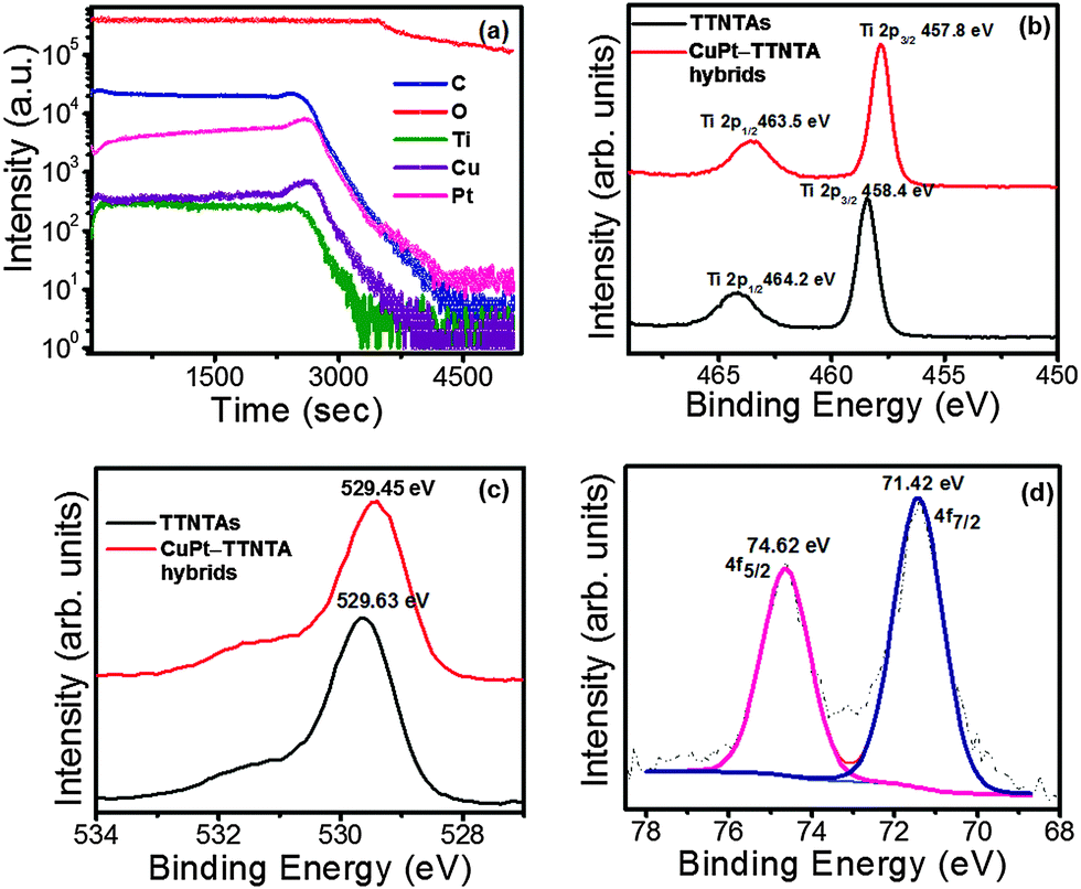 | ||
| Fig. 4 TOF-SIMS and XPS data from CuPt–TTNTA hybrids (a) TOF-SIMS and core-level spectra of (b) Ti 2p (c) O 1s and (d) Pt 4f. | ||
TOF-SIMS spectra (Fig. 4a) confirm the presence of all the materials present in the sample along with the substrate up to a sputtering time of ∼2600 s, which corresponds to the transition from the TiO2 nanotube barrier layer to the FTO layer below. Furthermore, the intensities of Cu and Pt obtained through SIMS profiling correlate well with that of Ti, indicating a fairly uniform loading of CuPt NPs along the nanotube walls with a slight increase in Pt concentration closer to the barrier layer. The core level spectra of Ti, O and Pt are seen in Fig. 4b–d. In Fig. 4b, the Ti 2p3/2 and Ti 2p1/2 states in TTNTAs present at 458.4 eV and 464.2 eV, respectively, correspond to Ti4+ states.56 The Ti4+ surface state shifts to 457.8 eV and 463.5 eV in CuPt–TTNTA hybrids. Fig. 4c displays the O 1s spectra with the presence of a Ti–O peak at 529.63 eV and 529.45 eV for TTNTAs and for CuPt–TTNTA hybrids, respectively. While the binding energy shift in this case appears to be a mere −0.18 eV, measurements over a number of samples and peak decomposition of the resulting O 1s spectra show that TTNTAs without an oxygen plasma treatment exhibit peaks at 531.90 eV and 530.14 eV, which correspond to O–Ti (3+) and HO–Ti (3+) respectively (Fig. S5 in the ESI†). Oxygen plasma treatment of the surface changes the relative weighting of the two peaks but leaves the peak positions almost unchanged (Fig. S5 in ESI†). On the other hand, photodeposition of CuPt consistently shifts both the peaks constituting the O 1s spectrum to lower binding energies (top panel of Fig. S6 in ESI†). This shift to lower binding energies after CuPt loading is characteristic of n-type semiconductors forming a Schottky junction with high work function metals, and occurs as a result of the lattice distortion of the TiO2 surface that generates oxygen vacancies. The oxygen vacancies in TiO2 correspond to the formation of Ti3+ states. Such a charge transfer process results in the shifting of binding energy of Ti to the lower energy side in CuPt–loaded TTNTAs. Measurements of multiple CuPt–TTNTA hybrid samples yielded a band bending of 0.4–0.7 eV from the shifts in the Ti 2p core-level spectra. The Pt 4f spectra can exhibit both initial and final state effects. The electric field due to the depletion region shifts the 4f7/2 and 4f5/2 peaks at 71.0 eV and 74.4 eV in bulk Pt to lower binding energies while the size-dependent screening effect shifts the peaks to higher binding energies. The width (FWHM) of the Pt 4f7/2 peak in bulk Pt is smaller than 0.5 eV. However, in Fig. 4d and for other samples of photodeposited CuPt–TTNTA hybrids (see Fig. S8a in ESI†), the FWHM is ca. 1.5 eV which is indicative of the presence of Pt clusters of size 1 nm and smaller.57 In Fig. 4d, the binding energy shifts in the two Pt 4f peaks are +0.2 to +0.4 eV. However, for samples with band bending towards the lower end of the range (0.4–0.5 eV), the peak shifts are +1.2 to +1.5 eV as shown in Fig. S8a in the ESI,† which we attribute to the final state effect being less obscured by the initial state effect.57 The data obtained by us strongly indicate that metallic behavior is not fully developed in the photodeposited CuPt nanoparticles.
 | ||
| Fig. 5 UPS spectra of CuPt–TTNTA hybrids. For each spectrum, the valence band maximum was estimated using the intercept on the abscissa obtained by extrapolating the low binding energy edge to the baseline. | ||
To understand the effect of Cu in CuPt–TTNTA hybrids, UPS data were collected from Pt–TTNTA hybrids wherein TiO2 nanotube arrays were coated with monometallic Pt nanoparticles using a near-identical photodeposition process. These data (see Fig. S12 in the ESI†) indicate the valence band edge in Pt–TTNTA hybrids to be shifted upward toward to the Fermi level by a much larger amount than in CuPt–TTNTA hybrids indicating a band bending as large as 1.6 eV. This observation can be rationalized using the Anderson model29 based on the much higher work function of monometallic Pt which is reduced by the addition of Cu in bimetallic alloys.
 | ||
| Fig. 6 Counter-clockwise from top (a) whole UPS spectra (b) magnified view of the secondary electron cut-off region and (c) valence band edges of transparent TiO2 nanotube samples following the photodeposition of CuPt NPs (red curve) subsequent to illumination under identical conditions in methanol but without the presence of metal precursors (purple curve). | ||
The deposition of CuPt nanoparticles is not purely a chemical reduction of the complexed Cu(II) and Pt(II) species in the respective acetylacetonates because the presence of ultraviolet radiation is essential. Therefore, the reaction is photo-induced, and it is possible to have one or both of photochemical reduction and photocatalytic deposition.63 In photochemical reduction, the illuminated solvent (MeOH, a potent hole scavenger) is the reducing agent and it is conceivable that the TiO2 too gets reduced in addition to the Cu(II) and Pt(II) ions. On the other hand, in photocatalytic deposition, it is illuminated TiO2 that is the reducing agent (through photogenerated electrons). Therefore, TiO2 can get oxidized at best but is more typically unchanged (since the reduction is performed by photogenerated excess charge carriers).56 The data presented here enable clear differentiation between the two phenomena under consideration. In particular, the band alignments produced by the photodeposition of CuPt on TiO2 nanotube arrays are shown to be totally different from the corresponding alignment produced by a pure photochemical reaction in methanol.
 | ||
| Fig. 7 Counter-clockwise from top-right (a–c): survey and magnified UPS valence band spectra of transparent TiO2 nanotubes (pink-colored curve), sputtered CuPt nanoparticles formed on transparent TiO2 nanotubes subsequent to oxygen plasma clean (green-colored curves) and sputtered CuPt nanoparticles formed on transparent TiO2 nanotubes without an oxygen plasma clean (blue-colored curves). In (d), the high resolution XPS core-level spectra of the Ti 2p peak are shown for sputtered CuPt nanoparticles formed on TiO2 nanotube arrays. | ||
The study of the interfacial band alignment in TTNTA:CuPt hybrids was accompanied by CO2 photoreduction studies and was compared with Sput-CuPt–TTNTA hybrids. Fig. 8a illustrates a photoreactor used for the reduction studies and the mechanism for a photoreduction process. The photoreduction of CO2 to CH4 is a complex that involves at least eight electron transfer steps. TTNTA:CuPt NPs demonstrated a higher CH4 yield (∼600 nmol cm−12 h−1) in comparison to TTNTAs coated with sputtered CuPt (∼30 nmol cm−2 h−1) for 6 hours of illumination under AM 1.5 one sun illumination, in agreement with previous reports.22,64 More details related to how this experiment was performed are provided in the ESI.† Despite CuPt–NPs not acting as electron sinks at moderate illumination intensities, such TiO2 nanotube–CuPt NP heterojunctions have demonstrated excellent performance for both photooxidation and photoreduction reactions. We hope our results will highlight the importance of the preparation technique on band alignment in heterojunctions and stimulate the search for reaction mechanisms where noble metals behave as hole-sinks.
 | ||
| Fig. 8 Schematic illustrations displaying the (a) photoreactor used for reduction experiments using TTNTA:CuPtNP hybrids as photocatalysts for the sunlight-driven conversion of CO2 into methane and (b) the conventional mechanism used to explain the conversion of carbon dioxide to methane by photoreduction on TiO2. | ||
The Schottky barrier height is given by ΦB = ϕbi + ϕn where ϕn (EC − EF) depends on the intrinsic carrier concentration in the n-TiO2 nanotubes and ϕbi is the maximum band-bending in the semiconductor. ϕbi is given by kT![[thin space (1/6-em)]](https://www.rsc.org/images/entities/char_2009.gif) lnNc/n where k is Boltzmann's constant and T is the absolute temperature, and estimated to be 0.06 eV at room temperature based on a conduction band density of states (Nc) of 1021 cm−3. In this study, we used TiO2 nanotubes formed in ethylene glycol electrolytes and annealed in air, for which a carrier concentration (n) in the range 1.4 × 10¹⁹–3.5 × 1020 cm−3 has been measured.69,70 The bandgap (Eg) of anatase phase TiO2 nanotubes (3.32 eV) is known to be slightly larger than that of bulk anatase.32,71 Thus, a range of 0.55–0.73 V is estimated for the Schottky barrier height. For a point-contact Schottky diode such as the one formed by isolated CuPt NPs decorating the walls of titania nanotube arrays, a hemispherical depletion region is obtained as shown in Fig. S10 (in the ESI†).72 We extracted the depletion region widths of such point-contact Schottky junctions with a barrier height of 0.4–0.7 V for 1 nm, 2 nm and 5 nm sized metal NPs for a range of equilibrium carrier concentrations in n-TiO2 (Fig. S11 in the ESI†). The resulting depletion widths are 2–10 nm (the inset of Fig. S11 in the ESI†). Since the wall-thickness of the TiO2 nanotubes is in the range 25–35 nm (see Fig. 2 and 3), the nanotubes will not be fully depleted by the surface band bending.
lnNc/n where k is Boltzmann's constant and T is the absolute temperature, and estimated to be 0.06 eV at room temperature based on a conduction band density of states (Nc) of 1021 cm−3. In this study, we used TiO2 nanotubes formed in ethylene glycol electrolytes and annealed in air, for which a carrier concentration (n) in the range 1.4 × 10¹⁹–3.5 × 1020 cm−3 has been measured.69,70 The bandgap (Eg) of anatase phase TiO2 nanotubes (3.32 eV) is known to be slightly larger than that of bulk anatase.32,71 Thus, a range of 0.55–0.73 V is estimated for the Schottky barrier height. For a point-contact Schottky diode such as the one formed by isolated CuPt NPs decorating the walls of titania nanotube arrays, a hemispherical depletion region is obtained as shown in Fig. S10 (in the ESI†).72 We extracted the depletion region widths of such point-contact Schottky junctions with a barrier height of 0.4–0.7 V for 1 nm, 2 nm and 5 nm sized metal NPs for a range of equilibrium carrier concentrations in n-TiO2 (Fig. S11 in the ESI†). The resulting depletion widths are 2–10 nm (the inset of Fig. S11 in the ESI†). Since the wall-thickness of the TiO2 nanotubes is in the range 25–35 nm (see Fig. 2 and 3), the nanotubes will not be fully depleted by the surface band bending.
In the conventional understanding of photocatalysis, noble metal NPs act as electron sinks79,80 due to which the transfer of photogenerated electrons to reactants occurs primarily on metal surfaces while the high oxidizing power of photogenerated holes is used in reactions on TiO2 surfaces. The efficiency of charge-separation processes in such a scenario is kinetically controlled by parameters such as the minority carrier diffusion length, the photoinduced electron transfer rate to the metal, trapping cross-sections and time-constants, etc. However, our XPS studies of the CuPt–TiO2 interface in transparent TiO2 nanotube arrays (TTNTAs) coated with photodeposited CuPt NPs (CuPt–TTNTA hybrids) show the existence of a depletion region with a built-in potential of 0.49–0.67 V. Under actual photocatalytic reaction conditions, further variation of the interfacial electronic properties is possible due to the adsorption of reactant species. Notwithstanding this, the Schottky barrier at the CuPt–TiO2 interface detected by our studies would direct photoexcited electrons toward the TiO2 and photoexcited holes toward the CuPt NPs (Fig. S1 in ESI†), which would require a review of the commonly accepted mechanistic routes for various photocatalytic reactions that are almost exclusively based on hole-mediated oxidation on TiO2 and electron-mediated reduction on the noble metal surface. The conventional model of noble metal electron sinks may still be applicable to the case of Sput-CuPt–TTNTA hybrids for which upward band bending was not detected.
Conclusions
The structure and electronic properties of the TiO2–noble metal interface are important in both photocatalysis and conventional catalysis. Most of the work in this area considers single crystals of rutile – reports on other forms and phases of TiO2 are scarce. Likewise, the majority of photoemission spectroscopic studies consider metal nanoparticles or films deposited under high vacuum conditions. However alternative methods of noble metal impregnation such as electrodeposition, photodeposition, wet impregnation, deposition–precipitation and colloidal synthesis are being extensively used to prepare photocatalysts, and the electronic properties of the resulting interfaces with semiconductor supports are largely unknown. Anodically formed TiO2 nanotube arrays coated with noble metal nanoparticles (NPs) formed by non-vacuum processes are being researched intensively for photocatalytic applications and have shown exceptional performance in recent studies. Cu–Pt bimetallic nanoparticles (NPs) were decorated over transparent TiO2 nanotube arrays via a facile approach of photodeposition to investigate their influence on the structural and electronic properties of CuPt–TTNTA hybrids. HRTEM studies revealed that Cu–Pt NPs were closely attached to the walls of TiO2 nanotubes. The crystalline structure of nanotubes and the local changes at the interface of CuPt–TTNTA hybrids were confirmed by microRaman spectroscopy. A shift in the Eg Raman mode along with a narrow broadening for CuPt–TTNTA hybrids was found due to the dispersion of bimetallic CuPt nanoparticles over TiO2 nanotubes. The lack of manifestation of metallic behavior in the XPS and UPS spectra was used to infer that the majority of photodeposited CuPt NPs had a size of 1 nm or smaller, even though 2–5 nm NPs were detected in electron micrographs. On the other hand, 2–5 nm sputtered and thermally dewetted CuPt manifested clear metallic behavior. The formation of a Schottky barrier at the CuPt–TiO2 interface with a band bending of 0.49–0.67 eV was confirmed through XPS and UPS studies in the photodeposited CuPt–TTNTA hybrids in comparison to sputtered CuPt–TTNTA hybrids, where no appreciable band bending was present. A close agreement between the band-bending values obtained from XPS and UPS results corroborates the formation of a depletion region at the photodeposited Cu–Pt TiO2 nanotube interface. This study also points to the strong effect of the preparation conditions of the noble metal promoter on the electronic structure of the resulting photocatalyst. We show that sputtered CuPt and photodeposited CuPt have substantially different band-alignment in heterojunctions with TiO2 nanotubes. Photochemical reduction by methanol was ruled out as a cause for the observed difference. On the other hand, the different size-scales of the sputtered and photodeposited CuPt nanoparticles were shown to be a contributing factor. Finally, the errors associated with the use of the term “Schottky barrier electron trapping” were highlighted.Acknowledgements
This project was funded through grants from the National Research Council of Canada (NRC) and NSERC. Some device fabrication and testing used research infrastructure made possible by a Leaders Opportunity Fund grant to K.S. from the Canada Foundation for Innovation (CFI) and the Alberta Small Equipment Grants Program (SEGP). Equipment use and staff assistance at the UofA NanoFab and the Alberta Centre for Surface Engineering and Science (ACSES) is acknowledged along with the funding obtained for user fees from CMC Microsystems. Measurement of the work functions and optical spectra of some samples by Ahmad Adl, synthesis of some TTNTAs by Abdelrahman Askar, and design of photocatalytic reactor and some CO2 photoreduction measurements by Xiaojiang Zhang are acknowledged. We also thank Prof. Jillian Buriak for helpful discussions.References
- K. Shankar, J. I. Basham, N. K. Allam, O. K. Varghese, G. K. Mor, X. J. Feng, M. Paulose, J. A. Seabold, K. S. Choi and C. A. Grimes, J. Phys. Chem. C, 2009, 113, 6327–6359 CrossRef CAS.
- T. E. Mallouk, J. Phys. Chem. Lett., 2010, 1, 2738–2739 CrossRef CAS.
- H. H. Mohamed and D. W. Bahnemann, Appl. Catal., B, 2012, 128, 91–104 CrossRef CAS.
- S. Valencia, F. Cataño, L. Rios, G. Restrepo and J. Marín, Appl. Catal., B, 2011, 104, 300–304 CrossRef CAS.
- K. Li, X. An, K. H. Park, M. Khraisheh and J. Tang, Catal. Today, 2014, 224, 3–12 CrossRef CAS.
- J. Pan, X. Wu, L. Wang, G. Liu, G. Q. Lu and H.-M. Cheng, Chem. Commun., 2011, 47, 8361–8363 RSC.
- Q. Zhai, S. Xie, W. Fan, Q. Zhang, Y. Wang, W. Deng and Y. Wang, Angew. Chem., Int. Ed., 2013, 52, 5776–5779 CrossRef CAS PubMed.
- A. Mohammadpour, P. Kar, B. D. Wiltshire, A. M. Askar and K. Shankar, Curr. Nanosci., 2015, 11, 593–614 CrossRef CAS.
- Q. Zhang, V. Celorrio, K. Bradley, F. Eisner, D. Cherns, W. Yan and D. J. Fermín, J. Phys. Chem. C, 2014, 118, 18207–18213 CrossRef CAS.
- J. R. Jennings, A. Ghicov, L. M. Peter, P. Schmuki and A. B. Walker, J. Am. Chem. Soc., 2008, 130, 13364–13372 CrossRef CAS PubMed.
- R. Mohammadpour, A. Iraji zad, A. Hagfeldt and G. Boschloo, ChemPhysChem, 2010, 11, 2140–2145 CrossRef CAS PubMed.
- G. K. Mor, K. Shankar, M. Paulose, O. K. Varghese and C. A. Grimes, Nano Lett., 2006, 6, 215–218 CrossRef CAS PubMed.
- X. Feng, K. Zhu, A. J. Frank, C. A. Grimes and T. E. Mallouk, Angew. Chem., Int. Ed., 2012, 51, 2727–2730 CrossRef CAS PubMed.
- K. Zhu, N. R. Neale, A. Miedaner and A. J. Frank, Nano Lett., 2006, 7, 69–74 CrossRef PubMed.
- M. H. Zarifi, A. Mohammadpour, S. Farsinezhad, B. D. Wiltshire, M. Nosrati, A. M. Askar, M. Daneshmand and K. Shankar, J. Phys. Chem. C, 2015, 119, 14358–14365 CAS.
- C. C. Mercado, F. J. Knorr, J. L. McHale, S. M. Usmani, A. S. Ichimura and L. V. Saraf, J. Phys. Chem. C, 2012, 116, 10796–10804 CrossRef CAS.
- G. Mie, Contributions to the optics of turbid media, particularly of colloidal metal solutions Transl. into ENGLISH from Ann. Phys.(Leipzig), v. 25, no. 3, 1908, p. 377–445, 1976, 1, 377–445.
- R. Gans, Ann. Phys., 1912, 342, 881–900 CrossRef.
- L. Li, P. A. Salvador and G. S. Rohrer, Nanoscale, 2014, 6, 24–42 RSC.
- N. T. Nguyen, M. Altomare, J. Yoo and P. Schmuki, Adv. Mater., 2015, 27, 3208–3215 CrossRef CAS PubMed.
- N. T. Nguyen, J. Yoo, M. Altomare and P. Schmuki, Chem. Commun., 2014, 50, 9653–9656 RSC.
- X. Zhang, F. Han, B. Shi, S. Farsinezhad, G. P. Dechaine and K. Shankar, Angew. Chem., 2012, 124, 12904–12907 CrossRef.
- B. Amirsolaimani, X. Zhang, F. Han, S. Farsinezhad, A. Mohammadpour, G. Dechaine and K. Shankar, MRS Online Proc. Libr., 2013, 1578 DOI:10.1557/opl.2013.841.
- W.-N. Wang, W.-J. An, B. Ramalingam, S. Mukherjee, D. M. Niedzwiedzki, S. Gangopadhyay and P. Biswas, J. Am. Chem. Soc., 2012, 134, 11276–11281 CrossRef CAS PubMed.
- X. J. Feng, J. D. Sloppy, T. J. LaTemp, M. Paulose, S. Komarneni, N. Z. Bao and C. A. Grimes, J. Mater. Chem., 2011, 21, 13429–13433 RSC.
- K. S. Raja, Y. R. Smith, N. Kondamudi, A. Manivannan, M. Misra and V. Subramanian, Electrochem. Solid-State Lett., 2011, 14, F5–F8 CrossRef CAS.
- Q. H. Zhang, W. D. Han, Y. J. Hong and J. G. Yu, Catal. Today, 2009, 148, 335–340 CrossRef CAS.
- Q. Fu and T. Wagner, Surf. Sci. Rep., 2007, 62, 431–498 CrossRef CAS.
- R. L. Anderson, Solid-State Electron., 1962, 5, 341–351 CrossRef CAS.
- I. H. Tseng, W. C. Chang and J. C. S. Wu, Appl. Catal., B, 2002, 37, 37–48 CrossRef CAS.
- S. C. Roy, O. K. Varghese, M. Paulose and C. A. Grimes, ACS Nano, 2010, 4, 1259–1278 CrossRef CAS PubMed.
- Z. Li, J. Liu, D. Wang, Y. Gao and J. Shen, Int. J. Hydrogen Energy, 2012, 37, 6431–6437 CrossRef CAS.
- D. Liu, Y. Fernández, O. Ola, S. Mackintosh, M. Maroto-Valer, C. M. A. Parlett, A. F. Lee and J. C. S. Wu, Catal. Commun., 2012, 25, 78–82 CrossRef CAS.
- H. Irie, S. Miura, K. Kamiya and K. Hashimoto, Chem. Phys. Lett., 2008, 457, 202–205 CrossRef CAS.
- M. Liu, X. Q. Qiu, M. Miyauchi and K. Hashimoto, Chem. Mater., 2011, 23, 5282–5286 CrossRef CAS.
- F. Boccuzzi, A. Chiorino, G. Martra, M. Gargano, N. Ravasio and B. Carrozzini, J. Catal., 1997, 165, 129–139 CrossRef CAS.
- F. Boccuzzi, A. Chiorino, M. Gargano and N. Ravasio, J. Catal., 1997, 165, 140–149 CrossRef CAS.
- Y. Shiraishi, H. Sakamoto, Y. Sugano, S. Ichikawa and T. Hirai, ACS Nano, 2013, 7, 9287–9297 CrossRef CAS PubMed.
- L. Li, Z. Xu, F. Liu, Y. Shao, J. Wang, H. Wan and S. Zheng, J. Photochem. Photobiol., A, 2010, 212, 113–121 CrossRef CAS.
- J. Y. Park, H. Lee, J. R. Renzas, Y. Zhang and G. A. Somorjai, Nano Lett., 2008, 8, 2388–2392 CrossRef CAS PubMed.
- H. Chen, S. Chen, X. Quan, H. Yu, H. Zhao and Y. Zhang, J. Phys. Chem. C, 2008, 112, 9285–9290 CrossRef CAS.
- G. A. Somorjai, K. M. Bratlie, M. O. Montano and J. Y. Park, J. Phys. Chem. B, 2006, 110, 20014–20022 CrossRef CAS PubMed.
- Y. K. Lee, C. H. Jung, J. Park, H. Seo, G. A. Somorjai and J. Y. Park, Nano Lett., 2011, 11, 4251–4255 CrossRef CAS PubMed.
- M. W. Knight, Y. Wang, A. S. Urban, A. Sobhani, B. Y. Zheng, P. Nordlander and N. J. Halas, Nano Lett., 2013, 13, 1687–1692 CrossRef CAS PubMed.
- C. Clavero, Nat. Photonics, 2014, 8, 95–103 CrossRef CAS.
- J. S. DuChene, B. C. Sweeny, A. C. Johnston-Peck, D. Su, E. A. Stach and W. D. Wei, Angew. Chem., Int. Ed., 2014, 53, 7887–7891 CrossRef CAS PubMed.
- X. Ma, Y. Dai, L. Yu and B. Huang, ACS Appl. Mater. Interfaces, 2014, 6, 12388–12394 Search PubMed.
- J. Y. Park, S. M. Kim, H. Lee and B. Naik, Catal. Lett., 2014, 144, 1996–2004 CrossRef CAS.
- L. J. Brennan, F. Purcell-Milton, A. S. Salmeron, H. Zhang, A. O. Govorov, A. V. Fedorov and Y. K. Gun'ko, Nanoscale Res. Lett., 2015, 10, 1–12 CrossRef CAS PubMed.
- M. Anpo, Catal. Surv. Asia, 1997, 1, 169–179 CrossRef CAS.
- H. Yoo, C. Bae, Y. Yang, S. Lee, M. Kim, H. Kim, Y. Kim and H. Shin, Nano Lett., 2014, 14, 4413–4417 CrossRef CAS PubMed.
- L. Gomathi Devi and S. Girish Kumar, Cent. Eur. J. Chem., 2011, 9, 959–961 CAS.
- J. Kim, J. Lee and W. Choi, Chem. Commun., 2008, 756–758 RSC.
- S. K. Parayil, H. S. Kibombo, C.-M. Wu, R. Peng, T. Kindle, S. Mishra, S. P. Ahrenkiel, J. Baltrusaitis, N. M. Dimitrijevic, T. Rajh and R. T. Koodali, J. Phys. Chem. C, 2013, 117, 16850–16862 CrossRef CAS.
- J. Zhang, M. Li, Z. Feng, J. Chen and C. Li, J. Phys. Chem. B, 2005, 110, 927–935 CrossRef PubMed.
- G. Wang, H. Wang, Y. Ling, Y. Tang, X. Yang, R. C. Fitzmorris, C. Wang, J. Z. Zhang and Y. Li, Nano Lett., 2011, 11, 3026–3033 CrossRef CAS PubMed.
- W. Eberhardt, P. Fayet, D. M. Cox, Z. Fu, A. Kaldor, R. Sherwood and D. Sondericker, Phys. Rev. Lett., 1990, 64, 780–783 CrossRef CAS PubMed.
- M. H. Park, J. H. Li, A. Kumar, G. Li and Y. Yang, Adv. Funct. Mater., 2009, 19, 1241–1246 CrossRef CAS.
- K. M. Coakley, Y. Liu, C. Goh and M. D. McGehee, MRS Bull., 2005, 30, 37–40 CrossRef CAS.
- W. Mönch, J. Appl. Phys., 2010, 107, 013706 CrossRef.
- B. Henrist, N. Hilleret, C. Scheuerlein and M. Taborelli, Appl. Surf. Sci., 2001, 172, 95–102 CrossRef CAS.
- J. Chen, E. Louis, J. Verhoeven, R. Harmsen, C. J. Lee, M. Lubomska, M. van Kampen, W. van Schaik and F. Bijkerk, Appl. Surf. Sci., 2010, 257, 354–361 CrossRef CAS.
- C. Ruiz, R. G. González Huerta, M. A. Valenzuela and N. Alonso-Vante, Top. Catal., 2011, 54, 512–518 CrossRef.
- O. K. Varghese, M. Paulose, T. J. LaTempa and C. A. Grimes, Nano Lett., 2009, 9, 731–737 CrossRef CAS PubMed.
- W.-J. Lee, M. Alhosan, S. L. Yohe, N. L. Macy and W. H. Smyrl, J. Electrochem. Soc., 2008, 155, B915–B920 CrossRef CAS.
- S. H. Kang, Y.-E. Sung and W. H. Smyrl, J. Electrochem. Soc., 2008, 155, B1128–B1135 CrossRef CAS.
- D. C. Gleason-Rohrer, B. S. Brunschwig and N. S. Lewis, J. Phys. Chem. C, 2013, 117, 18031–18042 CrossRef CAS.
- T. C. Leung, C. L. Kao, W. S. Su, Y. J. Feng and C. T. Chan, Phys. Rev. B: Condens. Matter Mater. Phys., 2003, 68, 195408 CrossRef.
- P. Pu, H. Cachet, E. Ngaboyamahina and E. M. M. Sutter, J. Solid State Electrochem., 2013, 17, 817–828 CrossRef CAS.
- P. Kar, A. Mohammadpour, B. D. Wiltshire, A. M. Askar and K. Shankar, Curr. Nanosci., 2015, 11, 593–614 CrossRef.
- S. Kurian, H. Seo and H. Jeon, J. Phys. Chem. C, 2013, 117, 16811–16819 CrossRef CAS.
- H.-K. Lyeo, A. A. Khajetoorians, L. Shi, K. P. Pipe, R. J. Ram, A. Shakouri and C. K. Shih, Science, 2004, 303, 816–818 CrossRef CAS PubMed.
- S. Kim, S.-J. Hwang and W. Choi, J. Phys. Chem. B, 2005, 109, 24260–24267 CrossRef CAS PubMed.
- J. Lee and W. Choi, J. Phys. Chem. B, 2005, 109, 7399–7406 CrossRef CAS PubMed.
- W. Choi, Catal. Surv. Asia, 2006, 10, 16–28 CrossRef CAS.
- H. Park, J. Lee and W. Choi, Catal. Today, 2006, 111, 259–265 CrossRef CAS.
- J. Kim, D. Monllor-Satoca and W. Choi, Energy Environ. Sci., 2012, 5, 7647–7656 Search PubMed.
- V. P. Zhdanov and B. Kasemo, Surf. Sci., 1999, 432, L599–L603 CrossRef CAS.
- P. Sangpour, F. Hashemi and A. Z. Moshfegh, J. Phys. Chem. C, 2010, 114, 13955–13961 CrossRef CAS.
- W. Zhao, C. Chen, X. Li, J. Zhao, H. Hidaka and N. Serpone, J. Phys. Chem. B, 2002, 106, 5022–5028 CrossRef CAS.
Footnotes |
| † Electronic supplementary information (ESI) available: Experimental details and supplementary figures relating to the electronic band-structure, nanotube morphology, photoemission spectra and depletion region formation. See DOI: 10.1039/c5cp05679a |
| ‡ Both authors contributed equally to this study. |
| This journal is © the Owner Societies 2015 |