
 Open Access Article
 This Open Access Article is licensed under a
 Creative Commons Attribution 3.0 Unported Licence
A molecular switch based on the manipulation of 1,3-dichlorobenzene on Ge(001) between two adsorption sites by inelastic tunneling electrons†
A.
Wykrota
ab,
M.
Bazarnik
ab,
R.
Czajka
a and
K.
Morgenstern
*b
aInstitute of Physics, Faculty of Technical Physics, Poznan University of Technology, Piotrowo 3, 60-965 Poznan, Poland
bRuhr-Universität Bochum, Lehrstuhl für physikalische Chemie I, D-44780 Bochum, Germany. E-mail: karina.morgenstern@rub.de
First published on 9th October 2015
Abstract
Meta-dichlorobenzene is adsorbed on Ge(001) and investigated by low temperature scanning tunneling microscopy. The molecule is altered between two adsorption sites by inelastic electron tunneling manipulation. These adsorption sites differ largely in conductivity. The necessary energy for switching the molecule between the sites and its polarity dependence indicate that the manipulation is initiated by the electronic excitation of the molecule.
Introduction
Functionalization of metal and semiconductor surfaces with molecular switches is an emerging trend in nanotechnology aimed at nanoelectronic applications.1,2 Switches should be both reversible and bistable and there should be a possibility to repeatably trigger externally the interconversion between two states that differ in some physico-chemical properties. Several successful switches based on the isomerisation of molecules were demonstrated on surfaces,3 more recently also on a semiconducting surface.4 Apart from changes within a molecule, there exists the intriguing, but little explored, possibility to switch a molecule between two equally stable adsorption sites. In particular on technologically relevant semiconducting surfaces, covalent bonds lead to defined adsorption sites of molecules. The challenge of this approach is bi-stability, because a surface often offers a multitude of adsorption sites of different stabilities.Surprisingly, only a few studies about molecular switches exist on semiconductors and none to our knowledge on pristine Ge(001). The change of a hydrogen atom on a hydrogen passivated Si(100)-(2 × 1) surface between two neighboring sites is an early example.5,6 This site change was induced by scanning the surface at room temperature near the surface resonance, at −2.4 V. The change was somewhat arbitrary, but the relative position of the tip with respect to the hydrogen atom influenced the diffusion direction of the atoms. On pristine Si(100), two adsorption sites of a biphenyl molecule formed an elegant bistable switch.7 More recently, benzonitrile molecules were attached to metallic chains of indium atoms on Si(001) and their position and orientation were manipulated by STM.8 The other few examples of switches based on site changes are on metal surfaces. The motion of the Co atom between a fcc and a hcp lattice site at the tip of a CoCu linear structure on Cu(111) was deduced from tunneling noise spectroscopy, at a tiny threshold of 15 mV.9 This motion was assumed to be lowered of the diffusion barrier in the presence of the tip, a process known to contribute to lateral manipulation.10 Also, a CO2 molecule bonded to an immobile oxygen atom on Ag(100) changes between two adsorption sites only.11 Finally, the random orientation of prochiral molecules in the gas phase is converted into two possible enantiomers with equal probability. Interconversion between these two orientations on the surface presents another possibility of a bistable switch.12,13 Such switches on metallic surfaces can only be operated at low temperature, because the states lack thermal stability.
As far as Ge(001) is concerned, a Pt dimer was changed between four configurations, thus lacking bistability.15,16 Also, octanethiol, attached to the STM tip, was attached and detached to a Pt covered Ge(001) surface by adjusting bias voltage and separation between the tip and the substrate.17 A molecular switch on pristine Ge(001) between two bistable adsorption sites has not yet been discussed. This is surprising, because Germanium is discussed by ITRS (International Technology Roadmap for Semiconductors)18 as a future material in semiconductor technology for three reasons.19 First, the high carrier mobility is important for high speed devices. Second, its small band gap will lead to low energy consumption. Finally, a low process temperature allows the integration of temperature sensitive materials. It is thus highly desirable to propose possible molecules that adsorb on the Ge(001) surface in two stable adsorption geometries.
In this article, we adsorb meta-dichlorobenzene on Ge(001) and investigate its adsorption by low temperature scanning tunneling microscopy. The molecule binds via its two chlorine atoms to the Ge atoms of the p(2 × 2) surface reconstruction that are less protruding from the surface. Two distinctly different adsorption sites are revealed, on one dimer row and bridging two dimer rows. The conductivity of molecules in these two adsorption sites differs largely. The molecule is switched between the adsorption sites, i.e. conductivity states, reversibly by injecting electrons into the LUMO+1 of the molecule. We thus present a bistable, reversible molecular switch on Ge(001) with largely different conductivity.
Experimental methods
STM measurements are performed using a low-temperature STM under ultra-high vacuum conditions (base pressure ≤2 × 10⁻¹⁰ mbar).Clean, reconstructed Ge(001) surfaces were obtained by several cycles of Ar+ ion sputtering for 30 minutes (energy 0.75 keV, emission current 1 μA, and Ar pressure 3 × 10⁻⁵ mbar), followed by annealing steps at 1070 K for 5 min and 970 K for 15 min, following an established procedure.20 The defect density is around 4% defects/dimers.
Meta-dichlorobenzene (m-DClB) (100% purity in chromatography) is further degassed under vacuum conditions by several pump cycles in a separate chamber. The cleanliness of the molecules is monitored by quadrupole mass spectrometry of the vapour. The molecules are introduced into the main chamber, i.e. deposited onto the surface, only if the mass spectrum shows the molecule mass and traces of the dissociation products of the molecule only. Note that the hot filament of the mass spectrometer induces the dissociation. Consequently all hot filaments are turned off during deposition. Prior to opening the valve to the main chamber, a pressure of 10−7 mbar is established in the separate chamber. The molecules are deposited within 30 s on the surface held between 22 K and 25 K. After deposition the sample is transferred into the STM chamber, where the measurements are performed between 5 K and 6 K.
Results and discussion
Surface preparation
After surface preparation, the Ge(001) surface consists of broad terraces (Fig. 1a). As expected, dimer rows change orientation on neighboring terraces (Fig. 1b).20 Images at higher resolution reveal regions with p(2 × 2) and c(4 × 2) reconstruction with their characteristic zig-zag rows (Fig. 1c).21 The defect density is 1/(5 ± 1) per nm2. The majority of the defects are dimer vacancy defects that appear as depressions in the STM images.20 Such dimer vacancies are mainly either isolated or in neighboring pairs of dimer vacancies within the same dimer row.20 For our single molecule study the defects are of minor importance, because we only investigate those molecules that are well separated from the defects. Only these molecules are included in the analysis.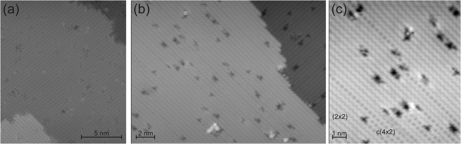 | ||
| Fig. 1 Ge(001) after the cleaning procedure and prior to molecule deposition at three different resolutions: (a) 1.806 V, 83 pA, (b) 1.619 V, 120 pA and (c) a region with p(2 × 2) reconstruction and a region with c(4 × 2) reconstruction are marked, 1.619 V, 210 pA. | ||
A small amount of meta-dichlorobenzene is deposited onto the Ge(001) surface. Meta-dichlorobenzene is a doubly chlorine substituted benzene in 1 and 3 positions (Fig. 2a, inset). The distance between the two chlorine atoms is 0.536 nm as calculated semi-empirically using the Parametric Method 7 parameterization of NDDO for the Hamiltonian for the gas phase molecule.22 Deposition of meta-dichlorobenzene on Ge(001) leads to protrusions that are randomly distributed over the surface (Fig. 2a and b). Agglomeration or island formation is not observed at the deposition temperature. Most prominent are ellipsoidal protrusions on top of dimer rows, at an apparent height of 150 pm at 1 V (Fig. 2c, blue rectangle). Note that there is a shallow increase in conductivity also on one of the neighboring double rows, here to the upper left of the molecule. Another change in contrast is much more subtle (Fig. 2c, red ellipsoid). This contrast consists of a pair of very shallow protrusions on neighboring double rows (Fig. 2c). Its apparent height is 55 pm only at 1 V. The pair of protrusions is hardly visible at many voltages (see below).
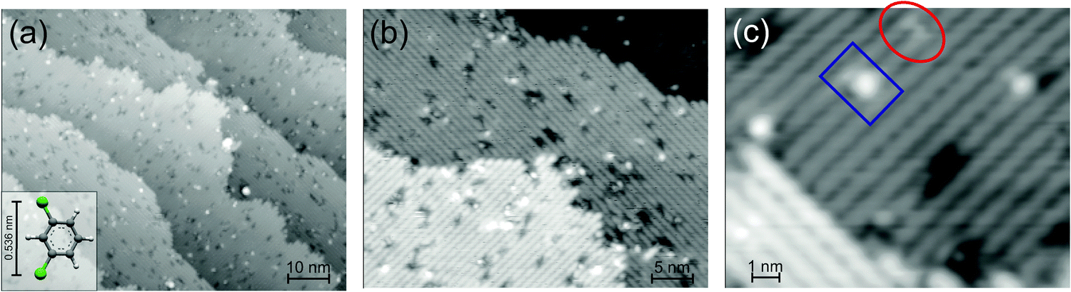 | ||
| Fig. 2 Ge(001) after the deposition of molecules at three different resolutions: (a) 1.62 V, 52 pA, inset: ball-and-stick model of the molecule as calculated semi-empirically using the Parametric Method 7 parameterization of NDDO for the Hamiltonian22 for the gas phase molecule. (b) 1.3 V, 40 pA and (c) molecules of two different contrasts are marked, 1.0 V, 10 pA. | ||
The two distinct shapes imply two adsorption sites of the molecule. We name the majority adsorption site the ‘high state’ and the minority adsorption site the ‘low state’, because the large difference in apparent height reflects a large difference in conductivity of the molecule in the two adsorption sites. The ratio of the two adsorption sites is estimated to lie between 1![[thin space (1/6-em)]](https://www.rsc.org/images/entities/char_2009.gif) :10 and 1:20 in favor of the high state by counting on images of high resolution.23
:10 and 1:20 in favor of the high state by counting on images of high resolution.23
The change to the neighboring row next to the bright protrusions of the high state is more obvious in highly resolved images at enhanced contrast (Fig. 3, marked by the blue rectangle). The image at higher resolution also reveals an asymmetry between the two protrusions of the low state (Fig. 3, marked by the red circle).
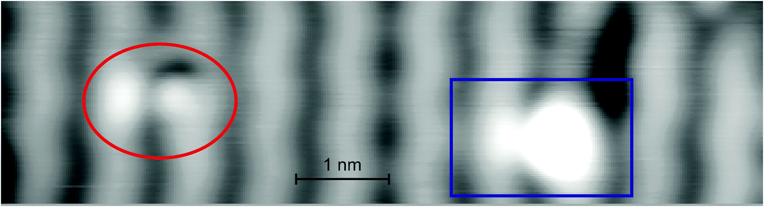 | ||
| Fig. 3 High-resolution STM image of molecules in two states with enhanced contrast: high state marked by the blue rectangle and low state marked by the red ellipsoid, 1 V, 11 pA. | ||
The adsorption site is determined by imaging a molecule with regular contrast and the same molecule with a so-called modified tip (Fig. 4). The resolution of both the Ge(001) reconstruction and the low state molecule is enhanced by unintentionally picking up one molecule during the manipulation intended to switch it (see below) (Fig. 4b). It allows imaging at lower voltage. Note that the voltage used is too small to achieve stable images on Ge(001) with a regular tip. The highly resolved image of the low state, at lower voltage and higher current than usually employed, resembles images of meta-dichlorobenzene adsorbed on Ag(111) and on Cu(111).24 The chlorine atoms are imaged as circular protrusions on both metallic surfaces. These protrusions are imaged off-center a larger protrusion that represents the phenyl ring. Based on these earlier results, we are thus able to determine the adsorption orientation of the low state; it is a meta-dichlorobenzene molecule that bridges two dimer rows as shown in Fig. 4c. We recently showed that meta-dichlorobenzene adsorbs via its two chlorine atoms also to the Au(111) surface.14 Here, the chlorine atoms are attached to those Ge atoms in the dimer rows that are imaged at smaller apparent height. It is well established that it depends on bias voltage, which of the two atoms of the dimer are imaged as more protruding. For the bias voltage used here, the image reflects the real height, i.e. the atoms that are more protruding are imaged at a larger apparent height.20 The chlorine atoms thus prefer adsorption to the less protruding atoms.
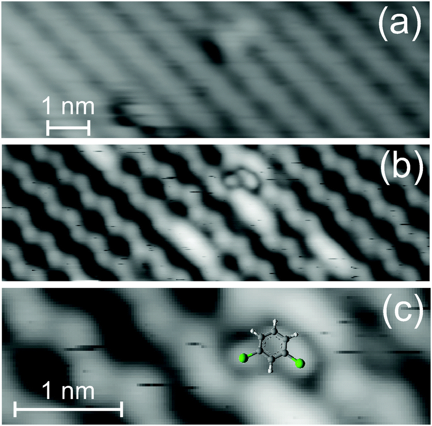 | ||
| Fig. 4 Image of the low state with (a) regular contrast, 1 V, 13 pA (b) modified tip, −0.6 V, 40 pA and (c) magnification of the image in (b) superimposed with the model of the molecule from Fig. 2a, inset, to scale. | ||
Unfortunately, molecules in the high state cannot be imaged reproducibly by the modified tip. Nonetheless, we are able to propose a model for the high state adsorption based on the low state model. The intensity of the high state is mainly on one dimer row, suggesting that both chlorine atoms are attached to the same dimer row. Indeed, the next-nearest neighbor distance in the row is very similar to the distance between the Germanium atoms, to which the chlorine atoms of the low state molecule bind (Fig. 5). It is reasonable to assume that the chlorine atoms bind preferentially to the low-lying Ge atoms in the dimer rows also in this case. Fig. 5 shows the suggested adsorption of the molecule on one dimer row. The additional conductivity of the dimer row next to the high state molecule (cf.Fig. 3) thus indicates the position of the benzene ring in images of regular resolution.
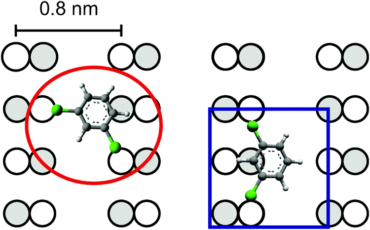 | ||
| Fig. 5 Model for the adsorption of meta-dichlorobenzene on Ge(001) (to scale) for the low state on left and for the high state on right; white and grey circles represent Germanium atoms, higher lying ones in grey. | ||
Manipulation of molecules
We now demonstrate that it is possible to externally trigger interconversion between the two states. For this aim, we use inelastic electron tunneling manipulation. Fig. 6a shows an image of a high state molecule adsorbed in one dimer row. We infer that the phenyl ring is to the right-hand side of the chlorine atoms from the small increase in apparent height on the neighboring dimer row. The molecule is changed to a low state molecule by injecting electrons up to an energy of 1.6 eV for 3.8 s (Fig. 6a and b). Thereby, the whole structure shifts downwards by approx. 0.3 nm. The corresponding change between the two adsorption sites is depicted in Fig. 6c, i.e. only one of the Ge–Cl bonds is broken and the other one serves as an anchor point during the switching motion.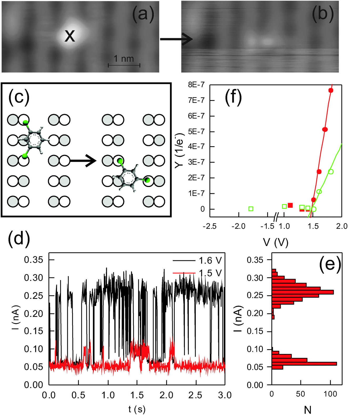 | ||
| Fig. 6 Manipulation of dichlorobenzene: (a and b) STM images; 1.1 V, 13 pA: (a) before manipulation at cross with energetic electrons up to 1.6 V for 3.8 s (current set point 30 pA), (b) after manipulation, (c) model for manipulation from (a) to (b), (d) I–t curves during manipulation at two different manipulation voltages as indicated, (e) histogram of the black I–t curve in (d) recorded at 1.6 V and (f) manipulation yield Y in dependence of manipulation voltage V; filled red symbols: from the low to high state; open green symbols: from the high to low state; circles are average yields; squares are upper limits of very low yields; lines serve to guide the eye. | ||
The current trace during manipulation shows clearly that the switch is bistable with the low current value corresponding to the low state molecule and the high current value to the high state molecule (Fig. 6d and e).26 The current ratio between the two states is four.
The controlled reproducibility of the switch is demonstrated in the manipulation series in Fig. 7. For three molecules, the low-state contrast is switched to the high state contrast, one molecule at a time (Fig. 7a–c). Two of the molecules are switched back as shown in Fig. 7d and e.
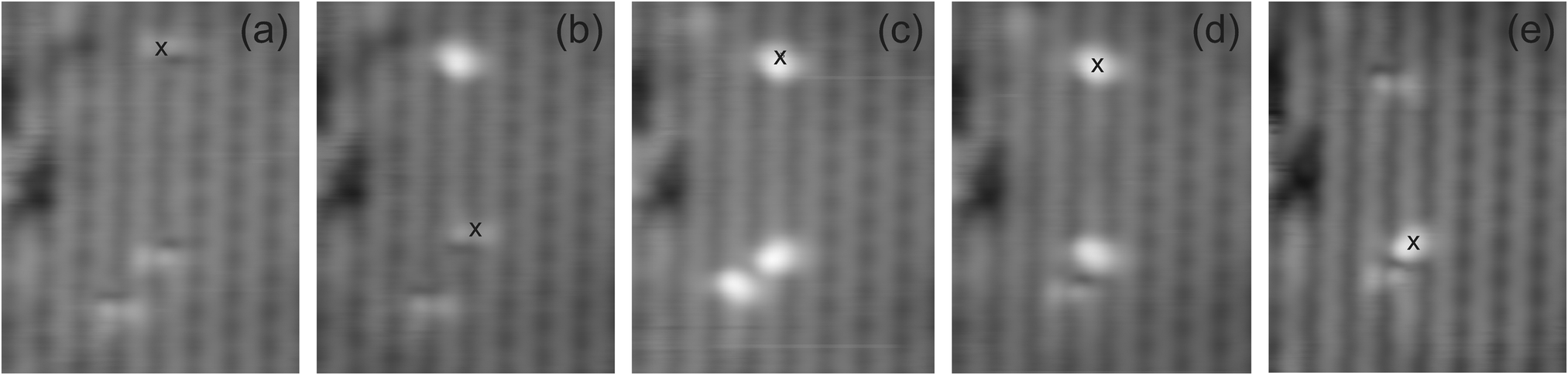 | ||
| Fig. 7 Manipulation series, imaging parameters: 1.1 V, 13 pA; manipulation parameters: (a to b): 1.8 V, 0.75 s (b to c) 1.5 V, 0.75 s (c to d) 1.5 V, 0.75 s and (d to e) 1.6 V, 0.75 s. | ||
I–t curves as shown in Fig. 6d allow us to determine the yield of the process. The voltage dependence of the yield reveals a threshold of 1.5 V for both switching directions, above which the switching yield increases with voltage (Fig. 6f). At all voltages, the switching yield is higher for the low current state than that for the high current state. This implies that the high current state is energetically preferred, in agreement with the larger ratio of high state molecules observed after adsorption (see above). We speculate on the preference for the high state based on the determined adsorption geometries. There are two differences between the two adsorption sites. First, there is a slightly different position of the chlorine atoms above the Ge atoms because of a small difference in distance between these two atoms. Second, the position of the benzene ring with respect to the underlying surface differs. As this ring is (most likely) adsorbed by van-der-Waals interaction and would thus prefer a larger distance to the surface than the chlorine atoms, it is more favorably positioned in the high state, where it is positioned between the rows than in the low state, where it is above a Ge atom. Moreover, this Ge atom is more protruding than the Ge atoms, to which the chlorine atoms bind. However, sophisticated calculations including van-der-Waals interaction are necessary for a definite answer.
Process determination
The threshold of 1.5 V lies in the range of molecular orbitals. Furthermore, the threshold is not symmetric around the Fermi energy. Even at −1.8 V the yield is below 5.6 × 10⁻⁹ per e− (Fig. 6f).27 Both observations suggest that the switching is initiated by an electronic excitation of the molecule, i.e. by injecting electrons into an unoccupied molecular orbital.28We use apparent height spectroscopy to determine the molecular orbitals involved in the electronic excitation. Apparent height spectroscopy plots the apparent height of a structure against voltage for voltage ranges covering molecular orbitals.25 It is possible to determine the position of molecular orbitals by apparent height spectroscopy, because the conductivity of molecules increases at molecular orbitals. Indeed, the images of the molecules depend on voltage (Fig. 8a and b). For instance, the protrusion on the neighboring row of the majority species is hardly visible at 1 V, but clearly at 1.6 V (Fig. 8a and b). It is most prominent at 1.8 V (Fig. 8c).
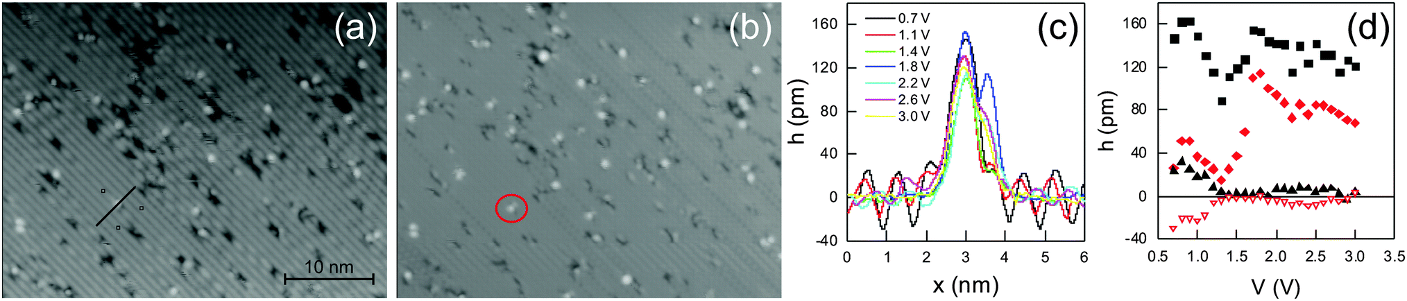 | ||
| Fig. 8 Voltage dependence of adsorbed molecules: (a and b) STM image at two different voltages; 16 pA: (a) 1 V, (b) 1.6 V, (c) line scans of the molecule marked in (b) along the line scan shown in (a) at selected voltages and (d) apparent height of the molecule marked in (b) and of the adjacent Ge surface in dependence of voltage: major protrusion of the molecule: black square; minor protrusion of the molecule: red diamond; highest point of the Ge surface: black up triangles; lowest point of the Ge surface: red down triangles. | ||
We analyze line scans, as shown in Fig. 8c, in order to determine the relative height of the two protrusions above the Ge surface, called major and minor protrusion in the following. Note that also the corrugation of the Ge dimer row structure is voltage dependent. The relative apparent heights of both protrusions above the Ge dimer rows show two maxima, at (0.85 ± 0.05) V and at (1.75 ± 0.05) V (Fig. 8d). Thereby, the relative height changes differ. The apparent height of the major protrusion above the Ge surface is, at 138 pm, more than five times the one of the minor protrusion, at 26 pm, for the maximum at (0.85 ± 0.05) V. The apparent heights differ by only ≈50% at (1.75 ± 0.05) V.
The two maxima in the apparent height spectra correspond to molecular orbitals. The orbital at (0.85 ± 0.05) V should have more weight at the chlorine atoms than the orbital at (1.75 ± 0.05) V and vice versa. Indeed the LUMO and the LUMO+1 of the gas phase molecule reflect this density distribution (Fig. 9).
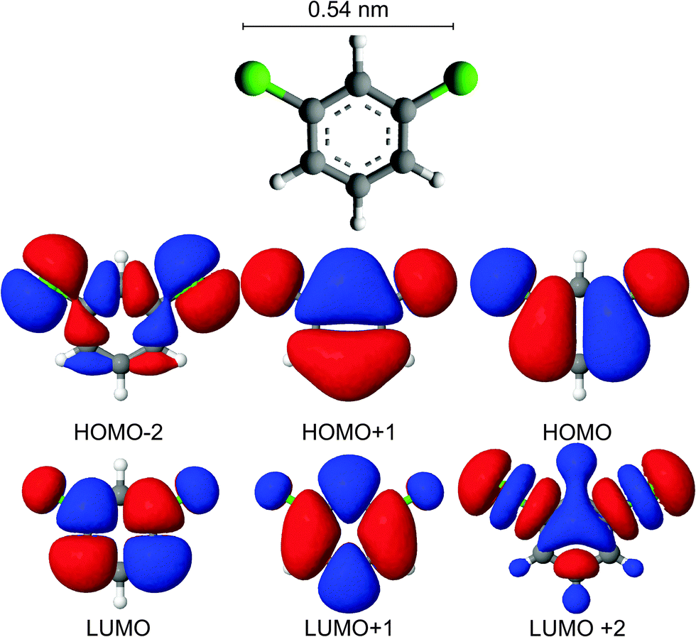 | ||
| Fig. 9 Molecular structure and orbitals calculated semi-empirically using the parametric method 7 parameterization of NDDO for the Hamiltonian22 for the gas phase molecule. | ||
The increase in apparent height spectroscopy close to the orbital at (1.75 ± 0.05) V (Fig. 8c) coincides with the threshold of the switch (Fig. 6e). We conclude that the adsorption site change is initiated by electrons attaching to the LUMO+1 orbital of the molecule.
Conclusions
In conclusion, we demonstrate that a doubly substituted benzene molecule has two adsorption sites on Ge(001) defined by specific bonding between the Ge atoms and the side groups. The sites differ geometrically. The high state molecules attach to one dimer row and the low state molecules attach to two neighboring dimer rows. The two stable adsorption sites of meta-diclorobenzene differ largely in conductivity. Electronic excitation allows us to manipulate the molecule between these two adsorption sites reversibly by breaking only one of the covalent bonds. This represents the first reversible molecular switch on a germanium surface to our knowledge. Our strategy to providing two defined points to anchor the molecule to a semi-conducting surface is applicable more generally. Moreover, we suggest to further modify the phenyl part of the molecule for a desired function.Acknowledgements
A.W., M.B., and K.M. gratefully acknowledge financial support from the German Academic Exchange Service, Polish Ministry of Science and Higher Educations under project no. IP2012 031772, and the German Science Foundation, respectively.References
- A. Aviram and M. A. Ratner, Chem. Phys. Lett., 1974, 29, 277 CrossRef CAS.
- C. Joachim, J. K. Gimzewski and A. Aviram, Nature, 2000, 408, 541 CrossRef CAS PubMed.
- K. Morgenstern, Acc. Chem. Res., 2009, 42, 213 CrossRef CAS PubMed.
- M. Bazarnik, L. Jurczyszyn, R. Czajka and K. Morgenstern, Phys. Chem. Chem. Phys., 2015, 17, 5366–5371 RSC.
- U. J. Quaade, K. Stokbro, C. Thirstrup and F. Grey, Surf. Sci., 1998, 415, L1037 CrossRef CAS.
- U. J. Quaade, K. Stokbro, R. Lin and F. Grey, Nanotechnology, 2001, 12, 265 CrossRef CAS.
- M. Lastapis, M. Martin, D. Riedel, L. Hellner, G. Comtet and G. Dujardin, Science, 2005, 308, 1000 CrossRef CAS PubMed.
- D. R. Belcher, M. W. Radny, St. R. Schofield, Ph. V. Smith and O. Warschkow, J. Am. Chem. Soc., 2012, 134, 15312 CrossRef CAS PubMed.
- J. A. Stroscio, F. Tavazza, J. N. Crain, R. J. Celotta and A. M. Chaka, Science, 2006, 313, 948 CrossRef CAS PubMed.
- U. Kürpick and T. S. Rahman, Phys. Rev. Lett., 1999, 83, 2765 CrossRef.
- M.-F. Hsieh, H.-D. Li, D.-S. Lin and K. Morgenstern, J. Phys. Chem. C, 2010, 114, 14179 Search PubMed.
- V. Simic-Milosevic, J. Meyer and K. Morgenstern, Angew. Chem., Int. Ed., 2009, 48, 4061 CrossRef CAS PubMed.
- M. Parschau, D. Passerone, K.-H. Rieder, H. J. Hug and K.-H. Ernst, Angew. Chem., Int. Ed., 2009, 48, 4065 CrossRef CAS PubMed.
- H. Gawronski and K. Morgenstern, Phys. Rev. B: Condens. Matter Mater. Phys., 2014, 89, 125420 CrossRef.
- A. van Houselt, R. van Gastel, B. Poelsema and H. J. W. Zandvliet, Phys. Rev. Lett., 2006, 97, 266104 CrossRef.
- A. Saedi, A. van Houselt, R. van Gastel, B. Poelsema and H. J. W. Zandvliet, Nano Lett., 2009, 9, 1733 CrossRef CAS PubMed.
- K. Sotthewes, V. Geskin, R. Heimbuch, A. Kumar and H. J W. Zandvliet, Appl. Phys. Lett., 2014, 2, 010701 Search PubMed.
- http://www.itrs.net, 2013.
- R. Pillarisetty, Nature, 2011, 479, 324 CrossRef CAS PubMed.
- H. J. W. Zandvliet, Phys. Rep., 2003, 388, 1 CrossRef CAS PubMed.
- H. J. W. Zandvliet, B. S. Swartzentruber, W. Wulfhekel, B. J. Hattink and B. Poelsema, Phys. Rev. B: Condens. Matter Mater. Phys., 1998, 57, R6803 CrossRef CAS.
- J. J. P. Stewart, J. Mol. Model., 2007, 13, 117312 CrossRef PubMed.
- The large uncertainty reflects the fact that the low state molecules are not clearly visible at all voltages and with all tips.
- V. Simic-Milosevic, J. Meyer and K. Morgenstern, Phys. Chem. Chem. Phys., 2008, 10, 1916 RSC.
- M. Mehlhorn and K. Morgenstern, New J. Phys., 2009, 11, 093015 CrossRef.
- The slightly different values of the high state current (black curve in Fig. 6d) are consistent with slightly different shapes of the molecule in the high state. These slight variations in current and image do not undermine the bistability of the switch as they are negligible compared to the changes in current and image between the low state and the high state. The histogram still shows two well separated states (Fig. 6e) regardless of the high state leading to a broader maximum.
- Note that the diffusion of the molecule is induced at both ±1.8 V.
- K. Morgenstern, N. Lorente and K.-H. Rieder, Phys. Status Solidi, 2013, 250, 1671 CrossRef CAS PubMed.
Footnote |
| † 68.37.Ef, 68.43.Jk, 68.43.-h. |
| This journal is © the Owner Societies 2015 |