
 Open Access Article
 This Open Access Article is licensed under a
 Creative Commons Attribution 3.0 Unported Licence
Charge carrier mobilities in organic semiconductors: crystal engineering and the importance of molecular contacts†
Asif
Bashir
a,
Alexander
Heck
bc,
Akimitsu
Narita
d,
Xinliang
Feng
d,
Alexei
Nefedov
e,
Michael
Rohwerder
a,
Klaus
Müllen
d,
Marcus
Elstner
bc and
Christof
Wöll
*e
aMax-Planck-Institut für Eisenforschung GmbH, 40237 Düsseldorf, Germany
bInstitute of Physical Chemistry, Karlsruhe Institute of Technology, 76131 Karlsruhe, Germany
cHEiKA – Heidelberg Karlsruhe Research Partnership, Heidelberg University, Karlsruhe Institute of Technology (KIT), Germany
dMax-Planck Institute for Polymer Research, 55128 Mainz, Germany
eInstitute of Functional Interfaces, Karlsruhe Institute of Technology, 76344 Eggenstein-Leopoldshafen, Germany. E-mail: christof.woell@kit.edu
First published on 27th July 2015
Abstract
We have conducted a combined experimental and theoretical study on the optimization of hexa-peri-hexabenzocoronene (HBC) as organic semiconductor. While orientations with high electronic coupling are unfavorable in the native liquid crystalline phase of HBC, we enforced such orientations by applying external constraints. To this end, self-assembled monolayers (SAMs) were formed by a non-conventional preparation method on an Au-substrate using electrochemical control. Within these SAMs the HBC units are forced into favorable orientations that cannot be achieved by unconstrained crystallization. For simulating the charge transport we applied a recently developed approach, where the molecular structure and the charge carrier are propagated simultaneously during a molecular dynamics simulation. Experiments as well as simulations are mutually supportive of an improved mobility in these novel materials. The implication of these findings for a rational design of future organic semiconductors will be discussed.
The recent success of organic light emitting diodes (OLEDs) in display technology further increases the demand for “all-organic” electronics. Indeed, it would be highly beneficial for the manufacturing process if the corresponding electronic circuitry driving the organic displays could also be made of organic material. The past decade has seen substantial progress in this field; organic molecules with extended π-conjugation have been successfully used as active semiconductors in devices like organic field effect transistors (OFETs).1–3
It is disturbing, however, that a satisfying understanding of the physical principles governing charge transport in organic materials is still missing. Whereas in disordered polymeric organic materials a hopping-transport of, both, electrons and holes prevails, the classical experiments carried out by Karl and coworkers demonstrated the presence of a “band-like” transport mechanism for both types of charge carriers in highly ordered, ultra-pure organic single crystals of mm-sized dimensions.4 It is obvious, however, that the concept of band-transport successfully used to describe charge transport in conventional inorganic semiconductors like Si and GaAs is inappropriate for organic semiconductor (OSC) materials. Previous theoretical work5,6 has demonstrated that the electronic bands in OSCs are essentially flat. For such a situation the conventional description predicts very low charge carrier mobility – the figure of merit of semiconductor materials. In accord with this striking failure, recent progress in the theoretical description of charge transport in organic materials has indicated that a completely different physical picture is needed to describe charge transport in organic materials. Most importantly, lattice vibrations have to be taken into account explicitly.7–9 For ordered crystalline systems model Hamiltonians have been established, where the interaction between molecules as well as the lattice dynamic are parametrized.10 As systems become more disordered however, the parametrization is no longer straight forward and these methods lose their predictive power. Clearly, a precise description of charge transport phenomena requires an atomistic simulation for the true (i.e. including thermally vibrations) structure. There are two main approaches to this problem. One is a molecular dynamic simulation of the morphology, wherefrom charge transfer parameters can be extracted. These are then further used in hopping models to describe the movement of the localized charge from one molecule to the other.11–15 The second path is the propagation of the electronic degrees of freedom using the time dependent Schrödinger equation, whereas the cores are propagated classically with non-adiabatic simulation schemes.16–18
Since charge transport in organic materials is also important to obtain a deeper understanding of organic light emitting diodes (OLED),19 organic solar cells20 and nanoscale molecular electronics, information on mobilities in organic materials as well as guiding principles to construct organic molecules with high mobilities are urgently required. Even more pressing is the need for rules with predictive power allowing for a rational design and synthesis of molecules with high charge carrier mobilities. Simplistic guiding principles like “best mobility values are obtained for planar molecules where π–π-interactions allow an optimal stacking” are valuable but are sometimes difficult to apply, e.g. when explaining the fact that some of the molecules showing the highest mobilities deviate substantially from planar geometries (e.g. rubrene21). Therefore, the search for organic molecules with high charge carrier mobilities has largely remained a trial-and-error effort.
Herein, we present new insight into the importance of the molecular packing in the condensed phase of π-bonded molecules, thus providing new guidelines for optimizing the performance of devices using organic semiconductors. We use a recently developed theoretical approach to demonstrate the important connection between molecular contacts and charge carrier mobilities for a particularly attractive semiconductor molecule, hexa-peri-hexabenzocoronene (HBC). This planar, fully conjugated hydrocarbon (Fig. S1, ESI†) can be regarded as a hexagonal “superbenzene” and has proven as prototype of molecularly defined nanographenes.22,23 What is especially important when using HBC as semiconductor component of devices is the straightforward attachment of substituents to the aromatic core: alkyl chains make the molecules solution or melt processable and phase forming, while (acetyl) thiol groups allow controlled anchoring to surfaces. We first consider the case of columnar arrangements of HBC_LC, (bearing six solubilizing alkyl chains at the periphery, Fig. 1a), which are realized e.g. in its liquid crystalline (LC) phases.24,25 It was realized quite early that the dynamic and actual structure of these materials play an important role.26 With regard to a theoretical description of charge transport, there is a general consensus that the electronic coupling between adjacent molecules is a crucial parameter. Importantly, however, previous work6,8 has shown that this parameter alone cannot provide a proper description but that vibrations within the rather soft organic materials have to be considered as well. In the current work the influence of the vibrations is explicitly captured by calculating the couplings along every step of molecular dynamic (MD) simulations.
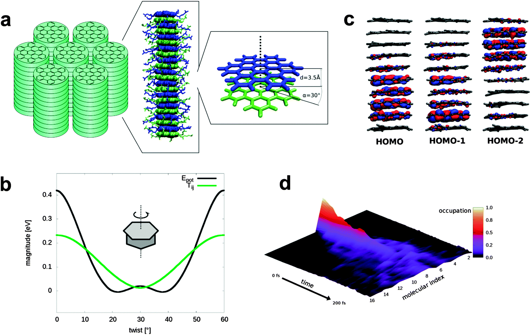 | ||
| Fig. 1 Electronic properties and simulation: (a) morphology of the liquid crystalline HBC derivate (HBC_LC). (b) Correlation of potential energy (black) with coupling (green) during rotation around the columnar axis prevents cofacial orientation with high couplings. (c) The three highest occupied molecular orbitals of HBC_LC, calculated at the HF/def2-SVP level for one geometry taken from a 10 ns molecular dynamics simulation. (d) Example of a charge propagation simulation. Like here, a fast diffusion of initially localized hole wave function can be observed in all simulations. | ||
A further crucial aspect in the theoretical treatment is the description of charge carrier motion. Here, the most commonly used approach is to consider charges localized on a single molecule and to describe their hopping by applying Marcus theory.27–31
Briefly, single charge carriers located on distinct molecules are allowed to hop to a neighbor if their energy is high enough. Earlier studies on HBC were only preformed with this methodology.14,32 It was shown, however, that this hopping mechanism is no longer applicable if the mobility surpasses ∼0.08 cm2 V−1 s−1 (ref. 33) which is the case in HBC derivatives.34,35 Furthermore, the assumption of localized charge carriers is not valid for stacked planar aromatic compounds like HBC since the HOMOs are delocalized over several molecules (Fig. 1c) even when dynamic disorder is considered. Due to the questionable applicability of hopping models for high mobility OSC, we use an Ehrenfest (mean field) approach for this system, where the charge carrier wave function is propagated according to time dependent Schrödinger equation and therefore free to delocalize (see Methods and ESI†).36,37 Similar methods were previously applied to ultra-fast transport in ordered crystalline systems and along polymer chains.16–18
One known problem of Ehrenfest simulations is, however, that the potential energy of the system is an average over all (adiabatic) states weighted by their occupation. The nuclear dynamic follows this mean potential energy surface (PES) instead of relaxing to a single adiabatic state. Therefore relaxation of the molecular structure will be progressively underestimated with the increasing degree of delocalization. This drawback is of significant importance when e.g. two adiabatic states with localized charge diverge in aqueous solution. The different PESs, arising from the respective adiabatic state, will differ significantly and propagating the atoms on an averaged PES will therefore lead to a qualitatively wrong dynamics. The PESs of delocalized charge carriers in a nonpolar environment, as found in organic semiconductors, are much more similar and averaging will therefore affect the nuclear dynamic and in turn the electron dynamic less severe. Furthermore, we derive the mobility from the beginning of the simulations where the charge is not as delocalized as at the end and the mean field error therefore smaller.
We first consider linear stacks as seen in liquid-crystalline (LC) phases HBC_LC (Fig. 1a). For this phase, where adjacent HBC units are rotated by 30° with respect to each other, mobilities of 0.5 cm2 V−1 s−1 were reported35 Considering that for other OSC materials like rubrene or pentacene values of above 40 cm2 V−1 s−1 have been reached,38 this value is fairly low – in apparent violation of the rule that cofacial packing of planar, fully conjugated π-systems should yield high mobilities (see above).
Our MD-simulations for such a columnar packing of HBC-units yield a mobility of 1.4 cm2 V−1 s−1 at 400 K. Increasing or decreasing the temperature by 50 K has only a minor effect on the mobilities (1.9 and 1.5 cm2 V−1 s−1 respectively) which is in accordance with the experiment and further confirms the applicability of the Ehrenfest method.39,40 The fact that the experimental mobilities are lower than the calculated ones can be explained by the influence of surface contamination, grain boundaries and defects,41–43 which are missing in our simulations but are always present in real samples, where they act as traps and obscure the intrinsic charge carrier mobility. Our simulations can be compared to earlier studies of Andrienko et al. on HBC liquid crystals, where Marcus-theory was applied to derive hole mobilities of 0.8 cm2 V−1 s−1 for similar LC with slightly different side chains.14 After adding environmental effects in form of energetic disorder the results became closer to experiment.32 For another liquid crystal with a larger aromatic core, mobilities of up to 15.9 cm2 V−1 s−1 were found in simulations without defects, a value which clearly overshoot is the experimental observable values.34
Besides the higher disorder in HBC liquid crystals compared to rubrene or pentacene, a further reason for the low mobility are the poor molecular contacts between neighboring molecules in the stacks. In (Fig. 1b) we show the HBC–HBC electronic coupling as a function of the twisting angle between adjacent HBC-cores in the columnar stacks forming the LC phase. Interestingly, the coupling for a direct, face-to-face packing with a twisting angle of 0° is substantially larger than the value of 13 meV for the twisting angle of 30° realized within the columnar stacks in the LC-phase.
It would be desirable to realize a direct face-to-face packing of the HBC-cores without rotations – and experiments for such systems should yield much higher mobilities. Such an arrangement is difficult to achieve, however, since it comes with a severe energy penalty (∼10 kcal mol−1 with 3.5 Å distance between HBC molecules calculated at the B3LYP-D/def2-TZVP level or theory) – the rotation by 30° is substantially more favorable and bulky side chains will further increase the energy penalty. Therefore this packing, optimal for charge carrier mobility, is not realized in an unconfined assembly leading to the rotated LC-phase. Clearly, more sophisticated strategies are needed to yield eclipsed columnar, 1-D stacks of HBC-cores.
Experiments on HBC single crystals are not suited for testing the importance of molecular contacts, since in the bulk structure of HBC such stacks are not present.44 In earlier experiments it was demonstrated, however, that molecular arrangements containing 1-d rows of HBC-cores could be realized in the form of self-assembled monolayers (SAMs) by employing HBC_C1, a HBC derivative to which one thiolate anchor and five solubilizing alkyl chains were attached.45 These HBC SAMs formed by spontaneous surface grafting were characterized by high-resolution microscopy (scanning tunneling microscopy, STM) and near edge X-ray absorption-spectroscopy (NEXAFS)45 and found to correspond to quasi-1D packing with twisting angles of 0° between adjacent cores. Here, the unfavorable intermolecular interaction is compensated through the boundary condition imposed by anchoring HBC-cores via the thiolate-groups to the Au-substrate, yielding stacks of tilted but eclipsed HBC cores.
It is unfortunate, however, that in this case ordering is not perfect, the HBC-units are rather shifted vertically relative to each other as a result of the Au(111) “herring-bone” reconstruction, which involves lateral (1.2 Å) and vertical (0.15 Å) shifts of the substrate atoms.46 Whereas for most thiolate-based SAMs this reconstruction has been found to be lifted, in this case it was still present and, as a result, a comparison of these results to the calculations discussed above is difficult. It should be noted, however, that in previous work high mobilities for these rows of 1d-stacked, tilted HBC-units were reported, which clearly exceed the values reported for the HBC LC phases. Obviously, the fact that the Au(111) reconstruction survives the HBC_C1 SAM-formation (HBC with mono thiolate-anchors) is a result of the fairly low density of the thiolate groups (149 Å2![[thin space (1/6-em)]](https://www.rsc.org/images/entities/char_2009.gif) (ref. 45) vs. 21.65 Å2 (ref. 47) for a normal, thiolate-based SAM). A straightforward strategy to overcome this problem is to add, by way of a new synthesis (see S2, ESI†) another thiolate-anchor to the HBC core since the stronger binding to the substrate (2 anchors instead of 1) should result in a substantially higher coverage of the thiolates within the SAMs thus forcing the graphene discs to realize a more perpendicular orientation (see Fig. 2).
(ref. 45) vs. 21.65 Å2 (ref. 47) for a normal, thiolate-based SAM). A straightforward strategy to overcome this problem is to add, by way of a new synthesis (see S2, ESI†) another thiolate-anchor to the HBC core since the stronger binding to the substrate (2 anchors instead of 1) should result in a substantially higher coverage of the thiolates within the SAMs thus forcing the graphene discs to realize a more perpendicular orientation (see Fig. 2).
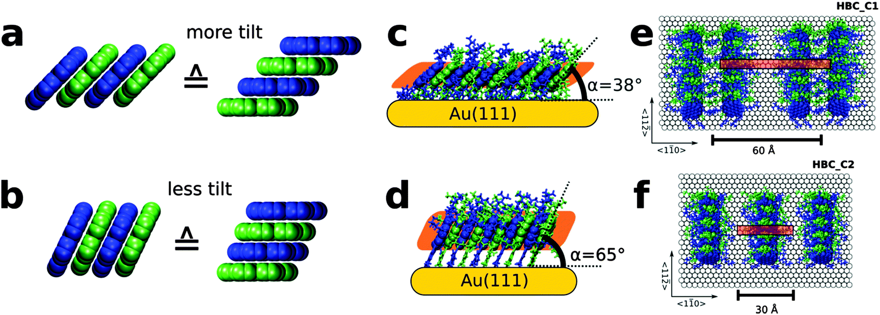 | ||
| Fig. 2 Effect of tilt angle on resulting lateral shift and packing density: (a and b) two different perspective views of HBC-discs showing the effect of tilt angle on the resulting lateral shift. (c) Side view of proposed structural model of mono-thiolate HBC (HBC_C1) and top view shown in (e). Side view of di-thiolate HBC SAM (HBC_C2) depicted in (d) and corresponding structural model in (f). | ||
Unfortunately, first attempts to grow SAMs from the corresponding HBC_C2 (with two anchors per HBC unit, see Fig. S1, ESI†) with high structural quality were unsuccessful (Fig. S4 and S5, ESI†). Even after an intense effort including a systematic variation of preparation conditions48,49 SAMs of sufficient quality could not be prepared. Similar difficulties have previously been reported for other dithiolate-based SAMs.50 In order to overcome these experimental problems we have therefore developed an unconventional, novel approach to obtain well-defined SAMs by using electrochemical control, i.e. by forming the SAM in an electrochemical cell with a well-defined potential applied.51 After varying the relevant parameters (voltage, concentrations), we finally succeeded in the preparation of well-defined SAMs also for the case of HBC_C2. Fig. 3 reveals the presence of columnar rows (for a structural model see Fig. 2f) with a high structural quality. We attribute the pronounced increase of lateral order in the thiolate-based HBC_C2 SAMs grown under electrochemical control to the slower kinetics, at a potential of −400 mV the adsorption process is critically slowed down (see earlier reports for alkanethiol-based SAMs51,52). This slower kinetics then allows for the annealing of defects, a process which is suppressed when the films are formed at higher speed in the absence of an electrochemical potential.
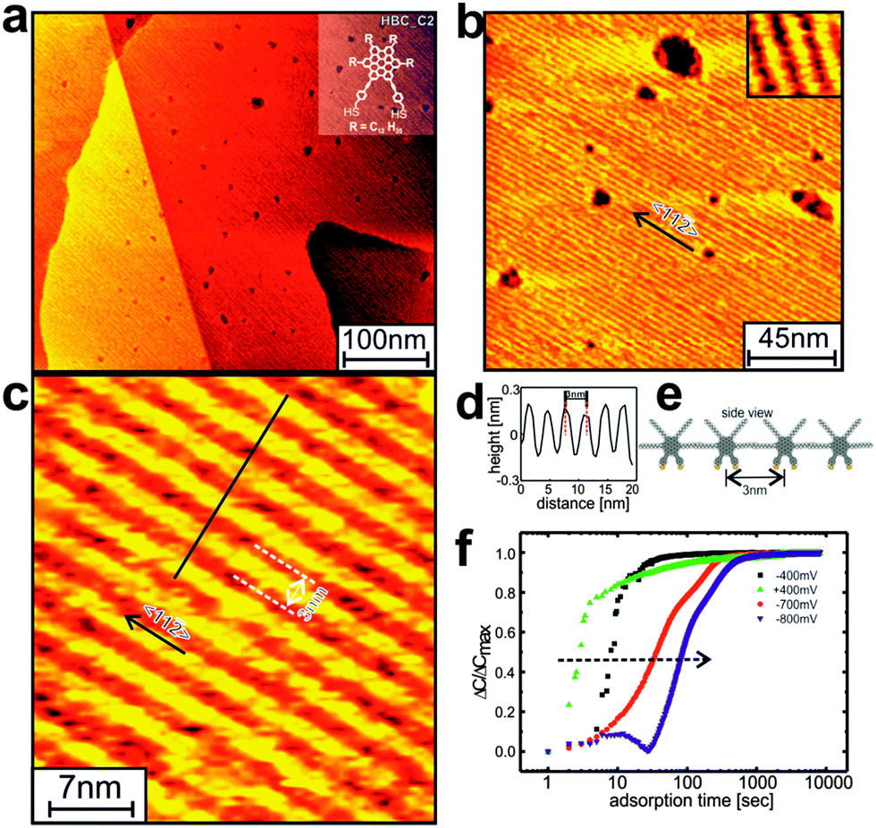 | ||
| Fig. 3 Summary of the data obtained for HBC_C2 SAMs prepared at room temperature under UPD at −400 mV: (a–c) STM micrographs of HBC_C2 SAMs at different magnification and high quality STM data presented as an inset in (b). Cross sectional height profile of line mark in (c) displayed in (d). The side view of proposed structural model indicating the separation of 3 nm between the lamellar rows illustrated in (e). (f) The trend of normalized capacity change versus adsorption time of HBC_C2 SAMs under UPD at −400 mV in nitrogen saturated ethanolic solution. | ||
Similar to the previous system,45 the STM data in Fig. 3 show extraordinary long range ordered domains of parallel lamella rows of HBC_C2 SAMs. Remarkable is the size of the ordered domains which are not limited by the monoatomic steps of the Au(111) substrate and exceed several hundred nanometers,. Note that the “etch pits” (or vacancy islands), a typical feature of thiolate-based SAMs with a characteristic depth of about 2.5 Å are clearly present, a feature which is not observed for the HBC_C1 thiols. We explain this difference by the fact that for the mono-anchored HBC_C1, the thiolate-density is so low that the Au(111)-reconstruction is not lifted. In the case of the di-anchored HBC_C2 the density of thiolate-units is twice as large, thus lifting the reconstruction and a corresponding appearance of vacancy islands.
A detailed analysis of the experimental data considering the NEXAFS data (see Section S6 and S7, ESI†) and the periodicity seen in the STM-data reveals a tilt angle of 65°, corresponding to a homogeneous lateral shift of 1.65 Å, see Fig. 2b and d.
Information on the charge carrier mobility within the HBC_C2-SAMs can be obtained by an investigation of the apparent height of HBC-islands embedded in an insulating matrix consisting of an alkanethiolate-SAM. A quantitative analysis of the apparent height of the OSC-islands as a function of island diameter (AHD-curves) provides information on the importance of lateral charge transport within these islands. Briefly, if there is no lateral transport, the height of these islands is simply given by the different lengths of the monomers forming the SAM (see Fig. 4), and there is no dependence of AH on diameter D. In the presence of finite lateral transport between adjacent molecules, the current injected form the STM-tip into the HBC-islands finds a smaller resistance (see the resistance network depicted in Fig. 4e), and as a result the AHD show a monotonic increase with diameter D displayed in Fig. 4d. By using the known dependence of tunneling current, and distance of the tip form the surface the AHD-curves can be simulated and a hole-mobility of 6.8 cm2 V−1 s−1 can be estimated (see ESI†). The increased mobility is in very reasonable agreement with the theoretical results (2.9 cm2 V−1 s−1) thus clearly demonstrating the importance of molecular contacts for charge transport in OSC materials. Note that while there is agreement between experiment and simulation regarding the relative mobilities of LC and SAM, there is still some deviation regarding the absolute value. The simulations overestimate the mobility for the LC, while for the SAM this value is underestimated, which might be explained by the respective amount of defects that can occur in the different materials. As verified by the STM data the SAM is nearly defect free, whereas it is known for the LC that the molecules undergo rotations around the columnar axis.53 In the simulations such large scale disorder is not accessible during finite sampling time. In the SAM, on the other hand, such motions are prohibited due to the grafting to the surface.
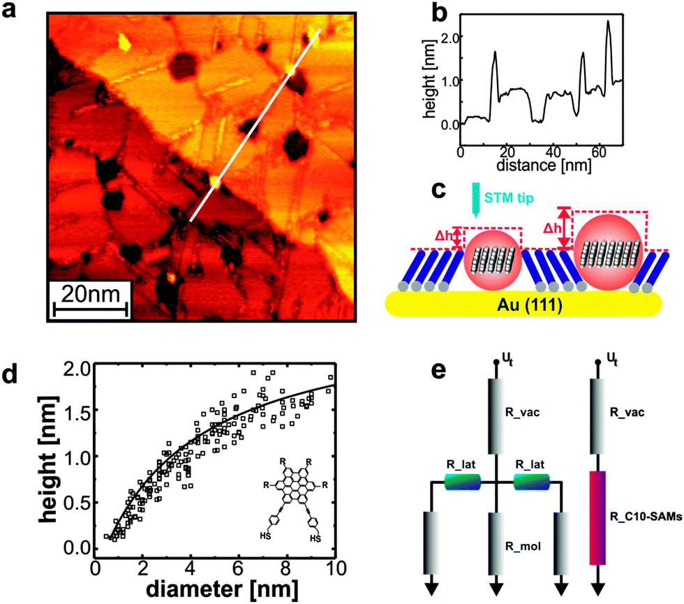 | ||
| Fig. 4 Apparent height vs. width correlations of islands obtained from HBC_C2-thiolate inserted in to decanethiol matrix: (a) HBC_C2 molecules as bright circular islands appeared either at step edges or domain boundaries and their corresponding line scan shown in (b). (c) Schematic cartoon showing the apparent height dependence (AH) vs. diameter (D) of OSC islands. (d) Pronounced height dependency on width of OSC islands clearly demonstrate the significance of later coupling between the stacked HBC molecules. (e) Schematic representation of tunneling junction of HBC-thiol with lateral resistance R_lat, and R_mol versus only the vertical resistance R_C10-SAMs in an insulation alkanethiol monolayers. Ut is tunneling voltage, R_vac denotes the vacuum gap, R_mol is the resistivity of single molecule and R_lat characterize the lateral resistance of the molecules. | ||
Although the present results have been obtained for quasi-1d systems they nevertheless allow one to draw important conclusions. First, the charge carrier mobilities for, both, holes and electrons depend crucially on the packing of the organic molecules. The lowest-energy configurations adapted without external boundary conditions typically do not result in high electronic overlaps, giving rise to low mobilities – even in the case of perfect, planar π-conjugated systems like nanographenes. Higher mobilities will be reached by crystal engineering via external boundary conditions – an approach which is expected to lead to dramatic increases in OSC charge carrier mobilities.
Conclusions
New insight into factors influencing charge carrier mobilities in OSC transfer was gained by computer-aided rational design of new materials. For a prototypical OSC-material, the nanographene HBC, the intermolecular electronic coupling, which governs charge carrier mobility, was shown to increase for molecular packings different from that adopted in the crystalline or liquid-crystalline phase. This theoretical prediction was validated experimentally by grafting appropriate functionalized HBC-discs to a substrate using an unconventional, electrochemically-controlled strategy. The intermolecular contacts in the grafted layers are shown to yield substantially higher mobilities. It stands to reason that crystal engineering providing molecular contacts optimized for intermolecular electronic coupling will become a guiding principle in the future development of high-mobility organic semiconductors. The implementation of this strategy will have to include a computer-based search for optimum molecular contacts as well as a substantial synthetic effort to add, as an enabling feature, functional side groups to “steer” the molecular packing.Methods
Sample preparation
Two types of substrates were used in this work.For the STM measurements freshly cleaved sheets of mica were heated up to 600 K for about 48 h inside the evaporation apparatus to remove residual water contained between the mica sheets. Subsequently, 150 nm of Au were deposited at a substrate temperature of 600 K under high vacuum conditions at ∼10−7 mbar. After deposition the substrates were allowed to cool down. Between substrate preparation and SAM formation the substrates were stored in an argon atmosphere. Immediately before the SAM formation the substrates were flame-annealed using a butane–oxygen flame. This procedure yielded Au substrates with well-defined terraces exhibiting a (111)-oriented surface. The terraces are separated by the steps of monoatomic height and have sizes in excess of 200 nm.
For the NEXAFS investigations, polycrystalline Au substrates were prepared by evaporating 5 nm of titanium (99.8%, Chempur) and subsequently 100 nm of gold (99.995%, Chempur) onto polished silicon wafers (Wacker) in an evaporation chamber (Leybold) operated at a base pressure of about ∼10−7 mbar. The thickness and the deposition rate 10 Å s−1 were monitored using a quartz crystal oscillator (Leybold Inficon). These substrates were stored in a vacuum desiccator until the adsorption experiments were carried out.
HBC_C2 molecules were formed in situ from an S-acetyl protected analogue, 2,5-bis[4-(S-acetylthiomethyl)phenylethynyl]-8,11,14,17-tetrakis(n-dodecyl)hexa-peri-hexabenzocoronene, which was synthesized as described in the ESI.† The HBC_C2 thiol was adsorbed on the Au electrodes were prepared by immersing Au substrates in a 0.1 μM dm−3 ethanol solution of the thiol for at least 30 hours at both RT (298 K) and HT (33 K). After the allotted immersion time, the samples were removed from solution and rinsed with pure acetone, ethanol and dried in a N2 stream. Decanethiol (C10-SH) SAMs were prepared by an 18 h or longer immersion in a 1 mM dm−3 ethanol solution containing C10-SH. The samples were withdrawn, rinsed in acetone, and ethanol, and dried in N2. The HBC_C2 molecules were embedded into C10-SH SAMs by immersing them in the ethanolic solution of HBC_C2 thiol.
STM
STM measurements were carried out in air using Agilent technologies 5500 and JSPM-4210 scanning probe microscope which was cross calibrated by imaging HOPG with atomic resolution. Tips were prepared mechanically by cutting a 0.25 mm Pt/Ir alloy (8:2, Chempur) wire. The STM data presented here were collected at room temperature in constant current mode using tunneling currents between 50 and 100 pA and a sample bias between 400 mV and 500 mV (tip positive). To reduce the drift, the samples were attached to the scanner 2 h before acquisition of the STM data. Under these tunneling parameters, no tip induced changes were observed by repeatedly scanning the same area several times.
Electrochemistry
All the electrochemical measurements were carried out in conventional three-electrode cell setup containing ethanolic solution of 0.1 μM dm−3 dithiol-HBC and 0.1 M LiClO4 by using potentiostat (Iviumstat, Ivium technology). The electrolytes were deaerated for half an hour by purging N2 prior to each experiment. The Au electrodes were introduced into the electrochemical cell which already contains solution of target molecules and LiClO4 under potential control (see text) using Ag/AgCl as a reference. The capacitance measurements were carried out by applying various bias potentials by alternating the electrode potential by ± 10 mV at a frequency of 10 Hz simultaneously monitoring the impedance modulus at 90° phase shift.NEXAFS
The NEXAFS measurements were performed at the dipole beamline HE-SGM of the synchrotron storage ring BESSY II in Berlin (Germany). All NEXAFS measurements were carried out with linearly polarized radiation (polarization factor P ≈ 91%) with an energy resolution of better than 350 meV. NEXAFS spectra were recorded at the C K-edge in the partial electron yield mode with a retarding voltage of −150 V. The NEXAFS raw data were normalized in a multi-step procedure by considering the incident photon flux, which was monitored by the photocurrent on the gold grid, and using the background signal of the clean Au substrate. A carbon-contamination of a gold grid with a characteristic peak at 284.81 eV was registered simultaneously with each spectrum and served as a reference for photon energy calibration. To determine the molecular orientation from the linear dichroism spectra were recorded for 5 different incidence-angles θ of the synchrotron radiation (θ = 20°, 30°, 40°, 55°, 70°, 90°) with respect to the surface.Non-adiabatic molecular dynamic simulations
In non-adiabatic simulations the electronic structure and nuclear motions are propagated simultaneously, which allows the nuclei to react to the instantaneous position of the charge as well as allowing a response of the charge carrier to the nuclear dynamics. The electronic degrees of freedom are propagated with the time dependent Schrödinger equation which allows delocalization of the charge carrier wave function, while the nuclear degrees of freedom can be propagated with Newton-like equations in a mean field (Ehrenfest) approach.In this work we use an efficient approximate non-adiabatic simulation scheme, which we have derived in the last years.36,37,54,55 A first approximation is reducing the quantum mechanical (QM) treatment to regions which are directly involved in the charge transport and describing the remainder of the system classically with molecular mechanic (MM) methods leading to a QM/MM approach. For the present system, the QM region consists of the aromatic cores of selected HBC molecules in one stack, while the side chains and the remaining HBC molecules in neighboring stacks are treated at the MM level. Second, due to the weak interactions between π-stacked molecules we partition the QM region in individual HBC molecules, which results in an efficient linear scaling of the method with system size. Third, only the highest occupied orbitals are relevant for hole transport and therefore all lower lying orbitals can be kept ‘frozen’ during the charge propagation. We then formulate a total energy expression for the charged system in the basis of molecular orbitals and derive equations of motions applying the Lagrangian formulism. 30 simulations were performed with starting structures taken from a 10 ns MD. In each simulation the tail of the hole wavefunction started to reach the end of the QM-zone after ca. 200 fs and the simulations were stopped. For details see the ESI.†
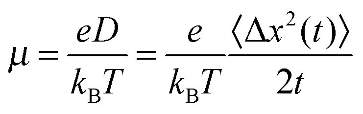
Simulated mobilities
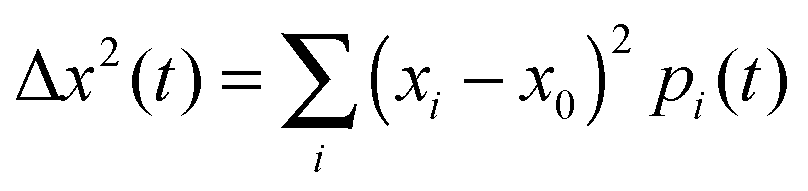
The mobility μ is derived from the displacement Δx of the charge at time t to its initial position:With the Boltzmann constant kB and the elementary charge e. The square displacement is defined as
with (xi − x0) denoting the distance of molecule i to the initially charge carrying molecule at position x0. The amount of charge on molecule i is given by
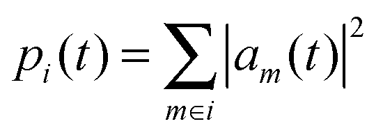 where am are the coefficients of the charge carrier wavefunction on molecule i. The final mean square displacement was obtained by averaging Δx2(t) over 30 simulations where 16 molecules in a stack were treated at the QM level. To average over dynamic disorder of the energy landscape, 5 equidistant starting structures along the 10 ns production runs were selected. In order to average over static disorder, for each starting structure the hole was initially created at 6 different molecules in the middle of the stack. Note that the degree of the initial localization on a single or few molecules was found to have minor impact on the obtained mobility.56 A linear fit of Δx2(t) vs. t was then used to obtain μ. An assessment of Ehrenfest simulations in the hopping regime showed that the qualitatively wrong mobilities can be obtained in the limit of infinite simulation times, whereas the mobility derived at the beginning of the simulation is still reliable.57 Therefore, only the first 100 fs were used for the fitting procedure. The resulting asymptotic standard error for the slope amounted to 1%. The fit is shown in the ESI.†
Notes and references
- S. R. Forrest, The path to ubiquitous and low-cost organic electronic appliances on plastic, Nature, 2004, 428(6986), 911–918 CrossRef CAS PubMed.
- G. Horowitz, Organic field-effect transistors, Adv. Mater., 1998, 10(5), 365–377 CrossRef CAS.
- A. Bayn, X. L. Feng, K. Müllen and H. Haick, Field Effect Transistors Based on Polycyclic Aromatic Hydrocarbons for the Detection and Classification of Volatile Organic Compounds, ACS Appl. Mater. Interfaces, 2013, 5(8), 3431–3440 CAS.
- N. Karl, Charge carrier transport in organic semiconductors, Synth. Met., 2003, 133, 649–657 CrossRef.
- J. L. Bredas, J. P. Calbert, D. A. da Silva and J. Cornil, Organic semiconductors: A theoretical characterization of the basic parameters governing charge transport, Proc. Natl. Acad. Sci. U. S. A., 2002, 99(9), 5804–5809 CrossRef CAS PubMed.
- F. Ortmann, F. Bechstedt and K. Hannewald, Charge transport in organic crystals: Theory and modelling, Phys. Status Solidi B, 2011, 248(3), 511–525 CrossRef CAS PubMed.
- V. Coropceanu, J. Cornil, D. A. da Silva, Y. Olivier, R. Silbey and J. L. Bredas, Charge transport in organic semiconductors, Chem. Rev., 2007, 107(4), 926–952 CrossRef CAS PubMed.
- V. Coropceanu, R. S. Sanchez-Carrera, P. Paramonov, G. M. Day and J. L. Bredas, Interaction of Charge Carriers with Lattice Vibrations in Organic Molecular Semiconductors: Naphthalene as a Case Study, J. Phys. Chem. C, 2009, 113(11), 4679–4686 CAS.
- Y. Li, V. Coropceanu and J. L. Bredas, Thermal Narrowing of the Electronic Bandwidths in Organic Molecular Semiconductors: Impact of the Crystal Thermal Expansion, J. Phys. Chem. Lett., 2012, 3(22), 3325–3329 CrossRef CAS.
- A. Troisi, Charge transport in high mobility molecular semiconductors: classical models and new theories, Chem. Soc. Rev., 2011, 40(5), 2347–2358 RSC.
- J. J. Kwiatkowski, J. Nelson, H. Li, J. L. Bredas, W. Wenzel and C. Lennartz, Simulating charge transport in tris(8-hydroxyquinoline) aluminium (Alq3), Phys. Chem. Chem. Phys., 2008, 10(14), 1852–1858 RSC.
- F. Gajdos, H. Oberhofer, M. Dupuis and J. Blumberger, On the Inapplicability of Electron-Hopping Models for the Organic Semiconductor Phenyl-C61-butyric Acid Methyl Ester (PCBM), J. Phys. Chem. Lett., 2013, 4(6), 1012–1017 CrossRef CAS.
- S. Difley, L. P. Wang, S. Yeganeh, S. R. Yost and T. Van Voorhis, Electronic Properties of Disordered Organic Semiconductors via QM/MM Simulations, Acc. Chem. Res., 2010, 43(7), 995–1004 CrossRef CAS PubMed.
- J. Kirkpatrick, V. Marcon, J. Nelson, K. Kremer and D. Andrienko, Charge mobility of discotic mesophases: A multiscale quantum and classical study, Phys. Rev. Lett., 2007, 98(22), 227402 CrossRef.
- V. Marcon, T. Vehoff, J. Kirkpatrick, C. Jeong, D. Y. Yoon, K. Kremer and D. Andrienko, Columnar mesophases of hexabenzocoronene derivatives. I. Phase transitions, J. Chem. Phys., 2008, 129(9), 094505 CrossRef PubMed.
- S. Stafstrom, Electron localization and the transition from adiabatic to nonadiabatic charge transport in organic conductors, Chem. Soc. Rev., 2010, 39(7), 2484–2499 RSC.
- M. V. A. da Silva, P. H. D. Neto, W. F. da Cunha, R. Gargano and G. M. E. Silva, Supersonic quasi-particles dynamics in organic semiconductors, Chem. Phys. Lett., 2012, 550, 146–149 CrossRef CAS PubMed.
- X. Gao, H. Geng, Q. Peng, J. J. Ren, Y. P. Yi, D. Wang and Z. G. Shuai, Nonadiabatic Molecular Dynamics Modeling of the Intrachain Charge Transport in Conjugated Diketopyrrolo-pyrrole Polymers, J. Phys. Chem. C, 2014, 118(13), 6631–6640 CAS.
- J. H. Burroughes, C. A. Jones and R. H. Friend, New Semiconductor-Device Physics in Polymer Diodes and Transistors, Nature, 1988, 335(6186), 137–141 CrossRef PubMed.
- P. Peumans, S. Uchida and S. R. Forrest, Efficient bulk heterojunction photovoltaic cells using small-molecular-weight organic thin films, Nature, 2003, 425(6954), 158–162 CrossRef CAS PubMed.
- A. Saeki, S. Seki, T. Takenobu, Y. Iwasa and S. Tagawa, Mobility and dynamics of charge carriers in Rubrene single crystals studied by flash-photolysis microwave conductivity and optical spectroscopy, Adv. Mater., 2008, 20(5), 920–923 CrossRef CAS PubMed.
- J. S. Wu, W. Pisula and K. Müllen, Graphenes as potential material for electronics, Chem. Rev., 2007, 107(3), 718–747 CrossRef CAS PubMed.
- L. Chen, Y. Hernandez, X. L. Feng and K. Müllen, From Nanographene and Graphene Nanoribbons to Graphene Sheets: Chemical Synthesis, Angew. Chem., Int. Ed., 2012, 51(31), 7640–7654 CrossRef CAS PubMed.
- A. Tracz, J. K. Jeszka, M. D. Watson, W. Pisula, K. Müllen and T. Pakula, Uniaxial alignment of the columnar super-structure of a hexa (alkyl) hexa-peri-hexabenzocoronene on untreated glass by simple solution processing, J. Am. Chem. Soc., 2003, 125(7), 1682–1683 CrossRef CAS PubMed.
- L. Piot, C. Marie, X. L. Feng, K. Müllen and D. Fichou, Hierarchical Self-Assembly of Edge-On Nanocolumnar Superstructures of Large Disc-Like Molecules, Adv. Mater., 2008, 20(20), 3854–3858 CrossRef CAS PubMed.
- I. Fischbach, T. Pakula, P. Minkin, A. Fechtenkotter, K. Müllen, H. W. Spiess and K. Saalwachter, Structure and dynamics in columnar discotic materials: A combined X-ray and solid-state NMR study of hexabenzocoronene derivatives, J. Phys. Chem. B, 2002, 106(25), 6408–6418 CrossRef CAS.
- R. A. Marcus, On the Theory of Oxidation-Reduction Reactions Involving Electron Transfer. 1, J. Chem. Phys., 1956, 24(5), 966–978 CrossRef CAS PubMed.
- R. A. Marcus, Electrostatic Free Energy and Other Properties of States Having Nonequilibrium Polarization. 1, J. Chem. Phys., 1956, 24(5), 979–989 CrossRef CAS PubMed.
- R. A. Marcus, Chemical + Electrochemical Electron-Transfer Theory, Annu. Rev. Phys. Chem., 1964, 15, 155–196 CrossRef CAS.
- R. A. Marcus and N. Sutin, Electron Transfers in Chemistry and Biology, Biochim. Biophys. Acta, 1985, 811(3), 265–322 CrossRef CAS.
- X. Yang, Q. Li and Z. Shuai, Theoretical modelling of carrier transports in molecular semiconductors: molecular design of triphenylamine dimer systems, Nanotechnology, 2007, 18(42), 424029 CrossRef PubMed.
- J. Kirkpatrick, V. Marcon, K. Kremer, J. Nelson and D. Andrienko, Columnar mesophases of hexabenzocoronene derivatives. II. Charge carrier mobility, J. Chem. Phys., 2008, 129(9), 094506 CrossRef PubMed.
- A. Troisi, The speed limit for sequential charge hopping in molecular materials, Org. Electron., 2011, 12(12), 1988–1991 CrossRef CAS PubMed.
- X. L. Feng, V. Marcon, W. Pisula, M. R. Hansen, J. Kirkpatrick, F. Grozema, D. Andrienko, K. Kremer and K. Müllen, Towards high charge-carrier mobilities by rational design of the shape and periphery of discotics, Nat. Mater., 2009, 8(5), 421–426 CrossRef CAS PubMed.
- A. M. van de Craats, J. M. Warman, A. Fechtenkotter, J. D. Brand, M. A. Harbison and K. Müllen, Record charge carrier mobility in a room-temperature discotic liquid-crystalline derivative of hexabenzocoronene, Adv. Mater., 1999, 11(17), 1469–1472 CrossRef CAS.
- T. Kubar and M. Elstner, A hybrid approach to simulation of electron transfer in complex molecular systems, J. R. Soc., Interface, 2013, 10(87), 1–18 CrossRef PubMed.
- T. Kubar and M. Elstner, Efficient algorithms for the simulation of non-adiabatic electron transfer in complex molecular systems: application to DNA, Phys. Chem. Chem. Phys., 2013, 15(16), 5794–5813 RSC.
- H. L. Dong, X. L. Fu, J. Liu, Z. R. Wang and W. P. Hu, 25th Anniversary Article: Key Points for High-Mobility Organic Field-Effect Transistors, Adv. Mater., 2013, 25(43), 6158–6182 CrossRef CAS PubMed.
- J. M. Warman and A. M. Van de Craats, Charge mobility in discotic materials studied by PR-TRMC, Mol. Cryst. Liq. Cryst., 2003, 396, 41–72 CrossRef CAS PubMed.
- A. M. van de Craats, J. M. Warman, M. P. deHaas, D. Adam, J. Simmerer, D. Haarer and P. Schuhmacher, The mobility of charge carriers in all four phases of the columnar discotic material hexakis(hexylthio)triphenylene: Combined TOF and PR-TRMC results, Adv. Mater., 1996, 8(10), 823–826 CrossRef CAS PubMed.
- O. D. Jurchescu, M. Popinciuc, B. J. van Wees and T. T. M. Palstra, Interface-controlled, high-mobility organic transistors, Adv. Mater., 2007, 19(5), 688–692 CrossRef CAS PubMed.
- J. Rivnay, L. H. Jimison, J. E. Northrup, M. F. Toney, R. Noriega, S. F. Lu, T. J. Marks, A. Facchetti and A. Salleo, Large modulation of carrier transport by grain-boundary molecular packing and microstructure in organic thin films, Nat. Mater., 2009, 8(12), 952–958 CrossRef CAS PubMed.
- M. Weis, K. Gmucova, V. Nadazdy, E. Majkova, D. Hasko, D. Taguchi, T. Manaka and M. Iwamoto, Grain Boundary Effect on Charge Transport in Pentacene Thin Films, Jpn. J. Appl. Phys., 2011, 50(4), 04DK03 CrossRef.
- R. Goddard, M. W. Haenel, W. C. Herndon, C. Kruger and M. Zander, Crystallization of Large Planar Polycyclic Aromatic-Hydrocarbons - the Molecular and Crystal-Structures of Hexabenzo[Bc,Ef,Hi,Kl,No,Qr]Coronene and Benzo[L,2,3-Bc/4,5,6-B′c′]Dicoronene, J. Am. Chem. Soc., 1995, 117(1), 30–41 CrossRef CAS.
- D. Käfer, A. Bashir, X. Dou, G. Witte, K. Müllen and C. Wöll, Evidence for band-like transport in graphene-based organic monolayers, Adv. Mater., 2010, 22(3), 384–388 CrossRef PubMed.
- C. Wöll, S. Chiang, R. J. Wilson and P. H. Lippel, Determination of Atom Positions at Stacking-Fault Dislocations on Au(111) by Scanning Tunneling Microscopy, Phys. Rev. B: Condens. Matter Mater. Phys., 1989, 39(11), 7988–7991 CrossRef.
- J. C. Love, L. A. Estroff, J. K. Kriebel, R. G. Nuzzo and G. M. Whitesides, Self-assembled monolayers of thiolates on metals as a form of nanotechnology, Chem. Rev., 2005, 105(4), 1103–1169 CrossRef CAS PubMed.
- D. Käfer, G. Witte, P. Cyganik, A. Terfort and C. Wöll, A Comprehensive Study of Self-Assembled Monolayers of Anthracenethiol on Gold: Solvent Effects, Structure, and Stability, J. Am. Chem. Soc., 2006, 128, 1723–1732 CrossRef PubMed.
- A. Bashir, D. Kafer, J. Muller, C. Wöll, A. Terfort and G. Witte, Selenium as a key element for highly ordered aromatic self-assembled monolayers, Angew. Chem., Int. Ed., 2008, 47(28), 5250–5252 CrossRef CAS PubMed.
- X. Stammer, K. Tonigold, A. Bashir, D. Käfer, O. Shekhah, C. Hulsbusch, M. Kind, A. Gross and C. Wöll, A highly ordered, aromatic bidentate self-assembled monolayer on Au(111): a combined experimental and theoretical study, Phys. Chem. Chem. Phys., 2010, 12(24), 6445–6454 RSC.
- M. Rohwerder, K. de Weldige and M. Stratmann, Potential dependence of the kinetics of thiol self-organization on Au(111), J. Solid State Electrochem., 1998, 2(2), 88–93 CrossRef CAS.
- T. Baunach, V. Ivanova, D. A. Scherson and D. A. Kolb, Self-assembled monolayers of 4-mercaptopyridine on Au(111): A potential-induced phase transition in sulfuric acid solutions, Langmuir, 2004, 20(7), 2797–2802 CrossRef CAS.
- I. Fischbach, T. Pakula, P. Minkin, A. Fechtenkotter, K. Mullen, H. W. Spiess and K. Saalwachter, Structure and dynamics in columnar discotic materials: A combined X-ray and solid-state NMR study of hexabenzocoronene derivatives, J. Phys. Chem. B, 2002, 106(25), 6408–6418 CrossRef CAS.
- T. Kubar and M. Elstner, Coarse-Grained Time-Dependent Density Functional Simulation of Charge Transfer in Complex Systems: Application to Hole Transfer in DNA, J. Phys. Chem. B, 2010, 114(34), 11221–11240 CrossRef CAS PubMed.
- T. Kubar, P. B. Woiczikowski, G. Cuniberti and M. Elstner, Efficient calculation of charge-transfer matrix elements for hole transfer in DNA, J. Phys. Chem. B, 2008, 112(26), 7937–7947 CrossRef CAS PubMed.
- L. Wang, D. Beljonne, L. Chen and Q. Shi, Mixed quantum-classical simulations of charge transport in organic materials: Numerical benchmark of the Su–Schrieffer–Heeger model, J. Chem. Phys., 2011, 134(24), 244116 CrossRef PubMed.
- L. Wang and D. Beljonne, Charge transport in organic semiconductors: Assessment of the mean field theory in the hopping regime, J. Chem. Phys., 2013, 139(6), 064316 CrossRef PubMed.
Footnote |
| † Electronic supplementary information (ESI) available. See DOI: 10.1039/c5cp03171k |
| This journal is © the Owner Societies 2015 |