
 Open Access Article
 This Open Access Article is licensed under a
 Creative Commons Attribution 3.0 Unported Licence
A microspectroscopic insight into the resistivity switching of individual Ag–TCNQ nanocrystals†
Benedikt
Rösner
a,
Ke
Ran
b,
Benjamin
Butz
b,
Ute
Schmidt
c,
Erdmann
Spiecker
b and
Rainer H.
Fink
*a
aDepartment Chemie und Pharmazie & ICMM, Friedrich-Alexander-Universität Erlangen-Nürnberg (FAU), Egerlandstr. 3, 91058 Erlangen, Germany. E-mail: rainer.fink@fau.de
bInstitute of Micro- and Nanostructure Research, Center for Nanoanalysis and Electron Microscopy (CENEM), Friedrich-Alexander-Universität Erlangen-Nürnberg (FAU), Cauerstr. 6, 91058 Erlangen, Germany
cWITec GmbH, Lise-Meitner-Str. 6, 89081 Ulm, Germany
First published on 11th June 2015
Abstract
We investigate the resistivity switching in individual Ag–TCNQ wires with on/off-ratios of up to 103. Raman and soft X-ray absorption microspectroscopy studies disclose reverse charge transfer. Quantifying of the fraction of neutral TCNQ within the switched material yields values up to 22.3%. These findings expedite the understanding of the switching process in Ag–TCNQ nanowires.
(7,7′,8,8′)-Tetracyanoquinodimethane (TCNQ) is a widely-known organic electron acceptor and readily forms charge transfer complexes with a wide range of metals, such as potassium, nickel, copper and silver. The molecule is thereby reduced to the stable radical anion and forms needle-shaped crystallites with the positively charged metal ion.1–6 Cu–TCNQ and Ag–TCNQ are the most prominent representatives of this class of materials: both materials have been intensely studied due to their exceptional electrical, magnetic and optical properties. Among these, the electrically bistable resistivity switching is of specific interest in molecule-based electronics, as the intrinsic resistivity of the naturally semiconducting materials can be electrically switched at a certain threshold voltage.3,7–11 This renders TCNQ charge transfer salts promising candidates for storage devices.9,12–14 The resistivity switching is linked to a structural phase transition which originates from the reverse electron transfer partly forming neutral Ag0 atoms and TCNQ0 molecules, which act as dopants in the charge transfer salt according to eqn (1).7,9
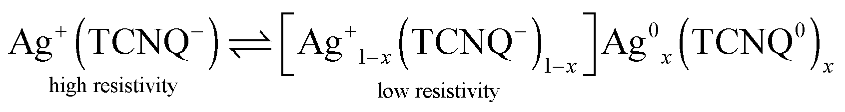 | (1) |
Within this work, we report on the resistivity switching and the underlying charge transfer mechanism in individual Ag–TCNQ crystallites in detail. Two complementary spectroscopic nanoprobes, i.e., near-edge X-ray absorption fine structure (NEXAFS) microspectroscopy and confocal Raman microspectroscopy, are employed to monitor changes in the spectroscopic fingerprints in operando. The dissimilar density of unoccupied states of the neutral TCNQ molecule and the respective radical anion thereby enables stoichiometric quantification of the reverse charge transfer upon switching within individual nanowires.
Results and discussion
Electrical characterization of individual Ag–TCNQ nanowires
There are basically two ways to prepare Ag–TCNQ crystallites which can be individually addressed using a microscope, namely the wet-chemical synthesis4,20 and a reaction from the vapour phase.21 Length and diameter distributions as well as morphologies and orientation can be tailored by varying the experimental parameters (see the ESI† for a detailed description of the sample preparation). Fig. 1a shows a TEM image of an upright standing nanowire on a gold substrate prepared via the gas phase reaction. The wires prepared using this method can be contacted by the tip of a scanning tunnelling microscope and electrically characterized inside the TEM. Fig. 1b shows an Ag–TCNQ wire prepared in solution and subsequently contacted with two gold pads as electrodes. These crystallites are larger in diameter (up to several micrometres) but exhibit comparable switching behaviour, and are thus utilized as model systems for Raman and NEXAFS spectroscopy studies in this work.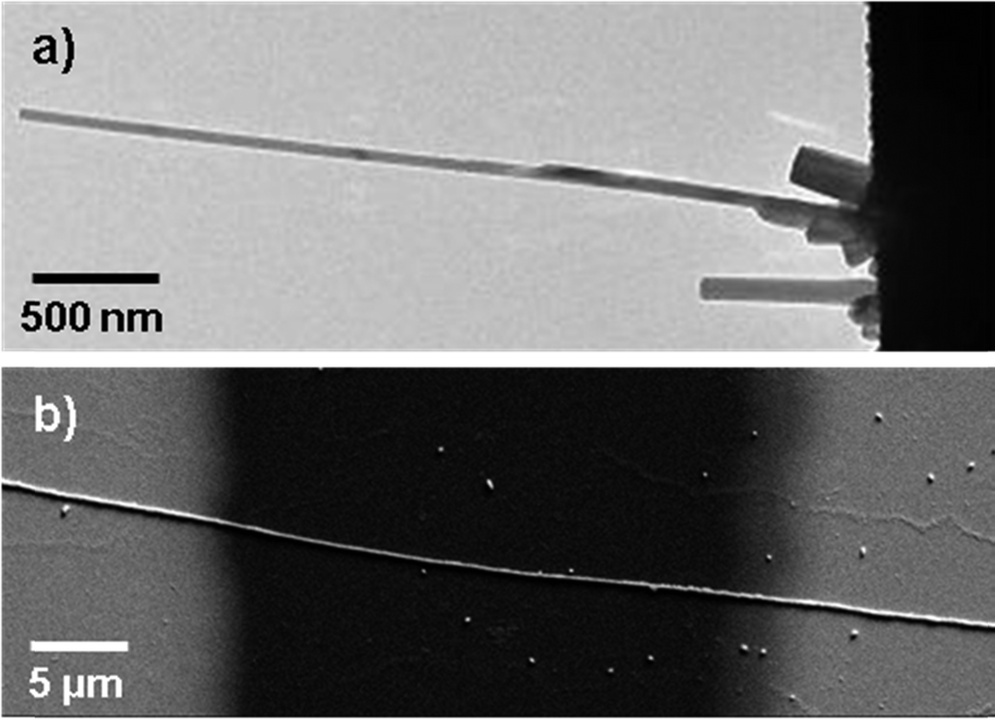 | ||
| Fig. 1 Individual Ag–TCNQ wires for microscopic and spectroscopic investigations in operando. (a) Transmission electron micrograph of an Ag–TCNQ nanowire (d = 41 nm) on a gold support, which can be contacted with a tungsten tip in the TEM. (b) Scanning electron micrograph of a crystallite (d = 0.35 μm) contacted with gold electrodes (the brighter areas on both sides). | ||
Fig. 2 shows the typical I–V characteristics of an individual Ag–TCNQ wire contacted inside the TEM indicating resistivity switching. Upon sweeping the voltage from 0 V to −10 V, the resistivity changes from a high resistance state to a low resistance state below −8 V. The subsequent, reverse voltage sweep shows a hysteresis-type behaviour, maintaining the low resistance state. Sweeping further to positive values, the current increases again, yet is more restrained than in the negative regime until it reaches comparable currents for forward and reverse sweeps at approx. 5.5 V. Upon taking a closer look to the on/off-ratios, the switching is evident. From negative voltages up to +2 V, the on/off-ratio well exceeds 102 (maximum value at −0.3 V: 1.15 × 10³), whereas it drops to values below 10 above 3.5 V. Thus, the on-state is induced by the negative voltage, and the material is brought back to its off-state by application of the positive voltage. The current is thereby limited to 10−7 A in order to protect the crystal from electrical breakdown (see below). Note that especially contributions from contact resistance in the experimental setup decrease the effective potential at the crystal itself; absolute values for the applied voltage have thus to be considered with care.
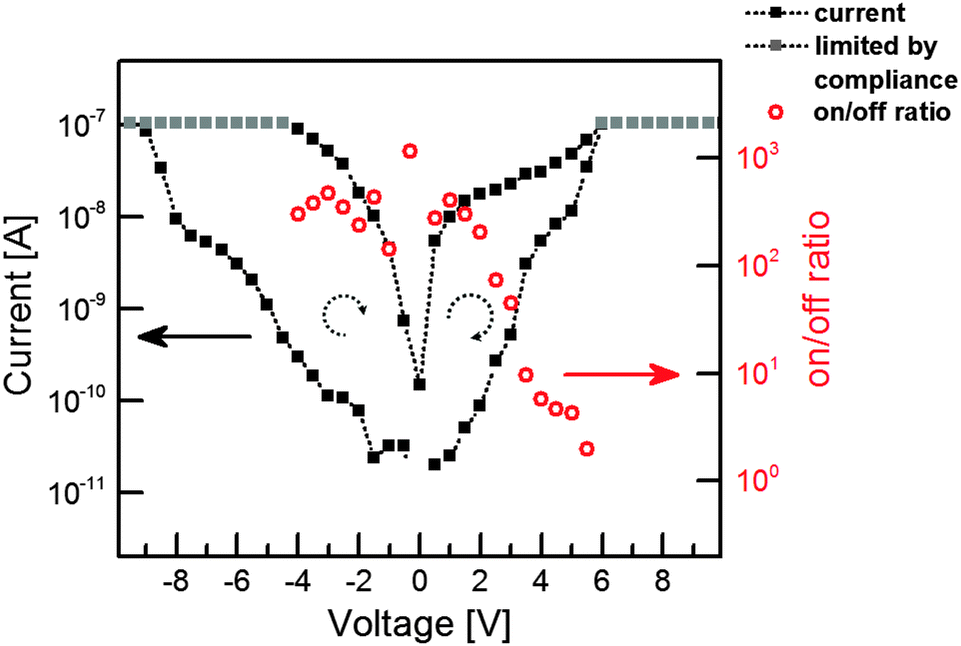 | ||
| Fig. 2 Current–voltage characteristics of an individual Ag–TCNQ crystallite. Negative and positive dual voltage sweeps have been conducted: 0 V → −10 V → 10 V → 0 V (black, squares). The on/off-ratios well exceed 102 (red, open circles). The on/off-ratios in the regime with limited current flow by the chosen compliance value (grey squares) cannot be determined and are therefore not shown. | ||
Probing the reverse charge transfer using Raman spectroscopy
A fundamental measure to probe and distinguish the state of TCNQ anions and neutral TCNQ molecules is their vibrational structure (see the ESI† for reference spectra from the pristine Ag–TCNQ and the neutral TCNQ species). Raman spectroscopy and theoretical considerations on TCNQ, Na–TCNQ and Cu–TCNQ3,22,23 allow us to assign the bands in the TCNQ and Ag–TCNQ spectra to distinct features. The bands at 1208 rel. cm−1 and 1605 rel. cm−1 represent vibrational modes within the TCNQ molecule, which are barely affected by the reduction to TCNQ− (ν3 and ν5 modes, ag symmetry).23 The TCNQ0 vibration at 1457 rel. cm−1 (C![[double bond, length as m-dash]](https://www.rsc.org/images/entities/char_e001.gif) C stretching mode, ν4, ag symmetry) is red-shifted to 1388 rel. cm−1 by the uptake of an electron into the lowest unoccupied (π*-)molecular orbital (LUMO), weakening the respective bonds due to antibonding effects. The electron is hereby located at one of the carbon atoms between the cyan groups and the quinone ring.24
C stretching mode, ν4, ag symmetry) is red-shifted to 1388 rel. cm−1 by the uptake of an electron into the lowest unoccupied (π*-)molecular orbital (LUMO), weakening the respective bonds due to antibonding effects. The electron is hereby located at one of the carbon atoms between the cyan groups and the quinone ring.24
Thus, we recorded the Raman spectra of individual Ag–TCNQ wires with various voltages applied to track the reverse charge transfer qualitatively (see Fig. 3). Whereas the spectral fingerprint remains unchanged at 1 V, the vibrational band at 1457 rel. cm−1, typical for neutral TCNQ, starts to increase at 5 V and appears more pronounced at 15 V, whereas the typical vibrational mode for the negatively charged molecule at 1388 rel. cm−1 decreases. This change is a direct spectroscopic proof that reverse charge transfer takes place when the resistivity state of an individual Ag–TCNQ wire is switched. The evolution of the characteristic band of the neutral TCNQ during voltage-induced resistivity switching demonstrates that a remarkable amount of the materials undergoes reverse charge transfer, forming the neutral species within the crystallite. However, an absolute quantification of affected molecules based on Raman spectroscopy is problematic even with the clear shift observed, due to dissimilar polarizability tensors of neutral and negatively charged molecules.25
 | ||
| Fig. 3 Reverse charge transfer probed using Raman spectroscopy. Raman spectra of an individual Ag–TCNQ wire under operation. With an increase in negative voltage (absolute values shown), the typical band for neutral TCNQ arises at 1457 rel. cm−1 whereas the vibration of the negative molecule at 1388 rel. cm−1 is diminished. | ||
Quantification by NEXAFS spectroscopy
Complementary to probing the vibrational structure, NEXAFS spectroscopy provides a powerful tool for investigating the chemical state of TCNQ. Both species, Ag–TCNQ and neutral TCNQ, are oriented equally with respect to the X-ray polarization to exclude effects which arise from linear X-ray absorption dichroism. Whereas Raman spectroscopy discloses a specific feature disparate for TCNQ− and TCNQ0, both the NEXAFS spectra of the reference materials show several strong and overlapping C 1s → π* absorption bands between 283 eV and 289 eV (Fig. 4a). The intensities and energy positions of the peaks show sufficient differences to distinguish the electronic states of TCNQ, especially the resonances of neutral TCNQ at 288.0 eV and 289.6 eV.26,27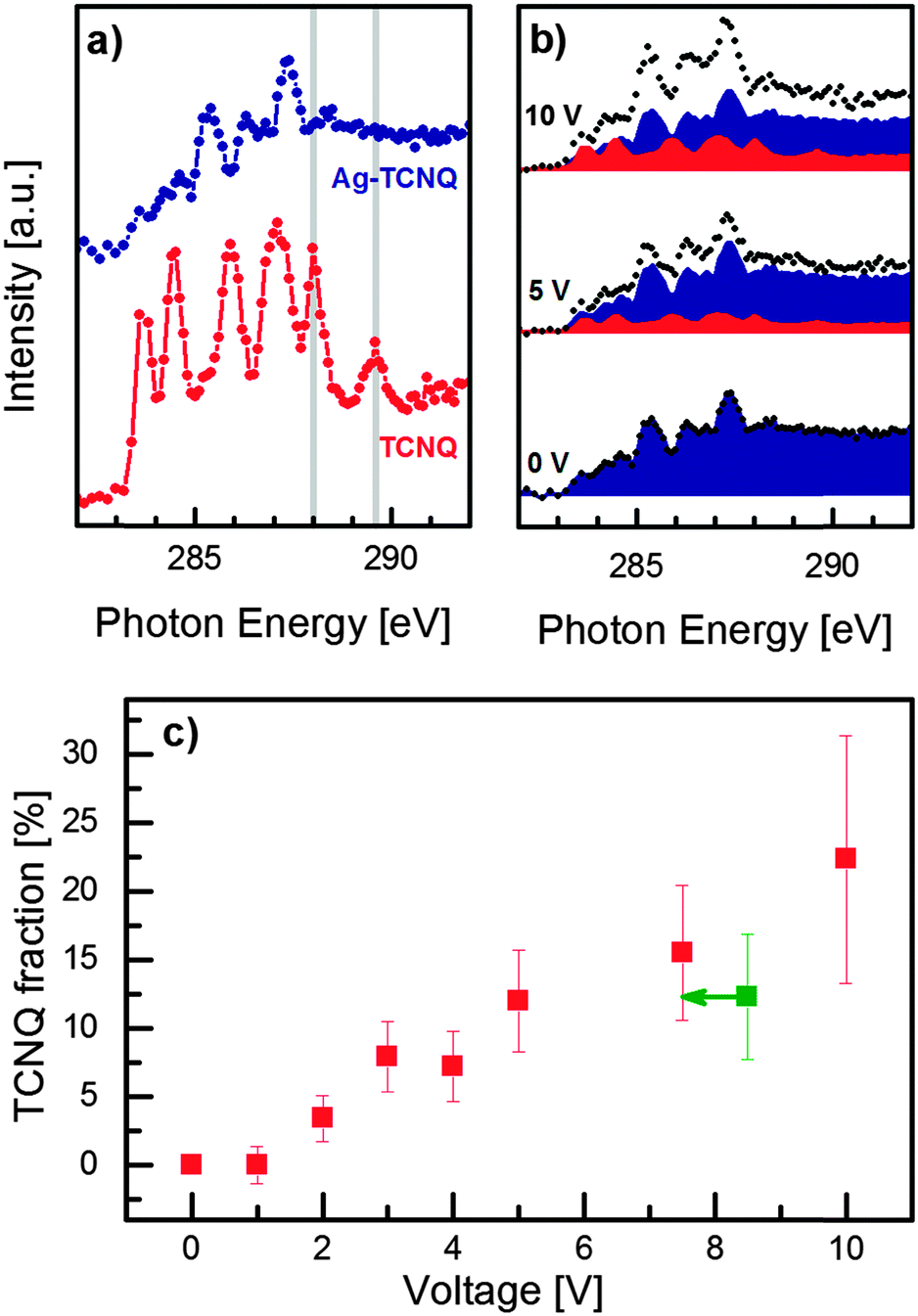 | ||
| Fig. 4 Quantification of the reverse charge transfer using NEXAFS spectroscopy. (a) Reference C K-edge NEXAFS spectra of TCNQ (red) and Ag–TCNQ (blue) recorded from the respective microcrystals. The typical resonances for TCNQ at 288.0 eV and 289.6 eV are indicated in grey. (b) Exemplary NEXAFS spectra of Ag–TCNQ (shown in Fig. 1b), (black dots) with different voltages applied. The underlying areas show the deconvolution of the Ag–TCNQ (blue) and neutral TCNQ contributions (red). (c) Fraction of neutral species (TCNQ0) as derived from spectral deconvolution. Note that the green data point corresponds to 7.5 V after five minutes of relaxation. | ||
The neutral TCNQ fraction in the Ag–TCNQ wire was derived as a function of applied voltage by linear combination (Fig. 4b, see ESI†). In this particular experiment, we obtain an increase in the TCNQ0 fractions up to 15.5 ± 4.9% (7.5 V, Fig. 4c). Most interestingly, the neutral TCNQ fraction remains in this range when the voltage is switched off (12.3 ± 4.6%) for five minutes, and increases further after 10 V has been applied for 1 min (22.3 ± 9.0%). Thus, NEXAFS confirms the findings from Raman spectroscopy that resistivity switching is accompanied by reverse charge transfer from the radical TCNQ anion to silver. Moreover, the quantification of this effect becomes possible using thickness-normalized spectra, yet with non-negligible uncertainty. Minor geometric modifications in the TCNQ moieties upon switching affect the absorption probability, which we consider in the experimental error. Nevertheless, the high percentages exceed those of typical dopants in semiconductors by far, indicating that the mechanism for resistivity switching is not a pure doping effect, but is more likely related to the accompanying structural rearrangement with inherent changes in the band structure.28 This structural change remains, however, concealed due to damage by electrons (in TEM) preventing a detailed electron diffraction analysis in the switched state.
Electrical breakdown and failure mechanism
High current densities lead to electrical breakdown of the nanowires. Typical currents exceed 10−7 to 10−6 A when the failure sets in. Substantial thinning and mechanical rupture of the Ag–TCNQ wires upon this process are revealed using TEM (see ESI†). We also observe the decomposition of the Ag–TCNQ crystallites upon too intense laser irradiation, accompanied by condensation of the neutral TCNQ around the crystal (see ESI†). These findings can be attributed to an excessive temperature increase by current-induced/resistive heating. With the reverse charge transfer during switching in the formation of the neutral TCNQ species, these extremely volatile molecules29 sublime and then condense in close vicinity of the crystallite, which leads to the observed thinning of the crystallites and finally to electrical breakdown. The experiments have therefore been performed with great care. The microspectroscopic imaging techniques employed here offer immediate inspection and control.Conclusions
The ability to contact and switch Ag–TCNQ crystallites with diameters down to tens of nanometres is a key step in advancing towards the implementation of this material into storage devices. Within this study, we demonstrate the reversible resistivity switching in individual, contacted Ag–TCNQ wires with on/off-ratios up to 103. The perspective to grow well-defined structures13,30 renders the materials appealing for the fabrication of structured arrays of switchable metal–organic nanowires.The use of microspectroscopic probes with high lateral resolution offers unique insights for investigating the resistivity switching in operando. Confocal Raman microscopy reveals the evolution of the vibrational band typical for neutral TCNQ molecules within the metal–organic salt upon voltage application. Essentially, the switching is accompanied by a remarkable reverse charge transfer from TCNQ− to the silver cations. These results confirm the mechanistic model that a mixed-valence state of the metal–organic TCNQ salt is an inherent precondition for the transition from the semiconducting high resistance state towards metallic conductivity.28 Moreover, NEXAFS spectroscopy enables the quantification of the neutral fraction as a function of the applied potential, yielding up to 22.3%. These values exceed the typical amounts for dopants in semiconductors by orders of magnitude. In light of these findings, an explanation for enhanced conductivity by structural rearrangements with inherent changes in the band structure28 seems plausible.
The potential benefit of this effect leading to switching of the resistance states is, however, limited by the heating and subsequent decomposition of the active Ag–TCNQ wires. This applies especially to crystallites with poor thermal coupling for sufficient heat dissipation. For the fabrication of respective electronic devices, encapsulation of the electrically active materials in an insulating, thermally conductive matrix to ensure structural stability of the contacted Ag–TCNQ moieties is therefore highly recommended.
Acknowledgements
We gratefully acknowledge Dr J. Raabe and Dr B. Watts (SLS) for technical assistance during STXM experiments. This work was funded by the DFG within the GRK 1896. BR acknowledges additional support from the Graduate School Molecular Science (GSMS). STXM experiments were partly funded within the European Community's Seventh Framework Programme (FP7/2007-2013) under grant agreement no. 312284 (CALIPSO). TEM experiments were partly funded by the DFG within the SFB 953 and the Cluster of Excellence EXC 315.Notes and references
- J. B. Torrance, B. A. Scott and F. B. Kaufman, Solid State Commun., 1975, 17, 1369–1373 CrossRef CAS.
- N. Uyeda, T. Kobayashi, K. Ishizuka and Y. Fujiyoshi, Nature, 1980, 285, 95–97 CrossRef CAS PubMed.
- R. S. Potember, T. O. Poehler and R. C. Benson, Appl. Phys. Lett., 1982, 41, 548–550 CrossRef CAS PubMed.
- G.-Y. Cao, C.-N. Ye, F. Fang, X.-Y. Xing, H.-H. Xu, D.-L. Sun and G.-R. Chen, Mater. Sci. Eng., B, 2005, 119, 41–45 CrossRef PubMed.
- G.-Y. Cao, F. Fang, C.-N. Ye, X.-Y. Xing, H.-H. Xu, D.-L. Sun and G.-R. Chen, Micron, 2005, 36, 285–290 CrossRef CAS PubMed.
- J. Song, Z. Ji, Q. Nie and W. Hu, Nanoscale, 2014, 6, 2573–2576 RSC.
- H. Wachtel, M. Ohnmacht, J. U. von Schütz and H. C. Wolf, Nanostruct. Mater., 1995, 6, 291–295 CrossRef CAS.
- S. A. O'Kane, R. Clérac, H. Zhao, X. Ouyang, R. J. Galán-Mascarós, R. Heintz and K. R. Dunbar, J. Solid State Chem., 2000, 152, 159–173 CrossRef.
- Z. Fan, D. Wang and J. G. Lu, IEEE Trans. Nanotechnol., 2003, 2, 588 Search PubMed.
- Q. Zhang, L. Kong, Q. Zhang, W. Wang and Z.-Y. Hua, Solid State Commun., 2004, 130, 799–802 CrossRef CAS PubMed.
- Q. Zhang, W. Wang, G.-F. Ye, X. Yan, Z. Zhang and Z.-Y. Hua, Synth. Met., 2004, 144, 285–289 CrossRef CAS PubMed.
- Z.-Y. Hua, G.-R. Chen, D.-Y. Chen and H.-H. Xu, IEEE Trans. Consumer Electron., 1998, 45, 97–100 Search PubMed.
- K. Xiao, J. Tao, A. A. Puretzky, I. N. Ivanov, S. T. Retterer, S. J. Pennycook and D. B. Geohegan, Adv. Funct. Mater., 2008, 18, 3043–3048 CrossRef CAS PubMed.
- B. Mukherjee, M. Mukherjee, J.-E. Park and S. Pyo, J. Phys. Chem. C, 2010, 114, 567–571 CAS.
- S. Shen, P. R. Ohodnicki, S. J. Kernion and M. E. McHenry, J. Appl. Phys., 2012, 112, 103705 CrossRef PubMed.
- V. DeGeorge, S. Shen, P. Ohodnicki, M. Andio and M. E. McHenry, J. Electron. Mater., 2014, 43, 96–108 CrossRef CAS PubMed.
- Z. Y. Fan, X. L. Mo, G. R. Chen and J. G. Lu, Rev. Adv. Mater. Sci., 2003, 5, 72–75 CAS.
- W. Zhou, L. Ren, F. Lin, L. Jiao, T. Xue, X. Xian and Z. Liu, Appl. Phys. Lett., 2008, 93, 123115 CrossRef PubMed.
- C. Wang, L. Wen, T. Kups, Y. Mi, R. Vellacheri, Y. Fang, P. Schaaf, H. Zhao and Y. Lei, J. Mater. Chem. C, 2013, 1, 8003–8006 RSC.
- B. Rösner, A. Späth and R. H. Fink, J. Cryst. Growth, 2013, 380, 34–38 CrossRef PubMed.
- C.-N. Ye, G.-Y. Cao, X.-L. Mo, F. Fang, X.-Y. Xing, G.-R. Chen and D.-L. Sun, Chin. Phys. Lett., 2004, 21, 1787–1790 CrossRef CAS.
- A. Girlando and C. Pecile, Spectrochim. Acta, Part A, 1973, 29, 1859–1878 CrossRef CAS.
- M. S. Khatkale and J. P. Devlin, J. Chem. Phys., 1979, 70, 1851–1859 CrossRef CAS PubMed.
- T. R. Umbach, I. Fernández-Torrente, M. Ruby, F. Schulz, C. Lotze, R. Rurali, M. Persson, J. I. Pascual and K. J. Franke, New J. Phys., 2013, 15, 083048 CrossRef.
- H. J. S. Machado and A. Hinchliffe, Electron. J. Theor. Chem., 1997, 2, 49–55 CrossRef PubMed.
- M. Bässler, R. Fink, C. Buchberger, P. Väterlein, M. Jung and E. Umbach, Langmuir, 2000, 16, 6674–6681 CrossRef.
- M. Koshino, H. Kurata and S. Isoda, J. Electron Spectrosc. Relat. Phenom., 2004, 135, 191–200 CrossRef CAS PubMed.
- J. B. Torrance, Acc. Chem. Res., 1979, 12, 79–86 CrossRef CAS.
- P. Tyagi, M. K. Dalai, C. K. Suman, S. Tuli and R. Srivastava, RSC Adv., 2013, 3, 24553–24559 RSC.
- K.-B. Zheng, X.-Y. Li, X.-L. Mo, G.-Y. Chen, Z.-D. Wang and G.-R. Chen, Appl. Surf. Sci., 2010, 256, 2764–2768 CrossRef CAS PubMed.
Footnote |
| † Electronic supplementary information (ESI) available: Materials and methods, crystallinity, data evaluation and quantification, reference spectra, decomposition of Ag–TCNQ. See DOI: 10.1039/c5cp02207j |
| This journal is © the Owner Societies 2015 |