
 Open Access Article
 This Open Access Article is licensed under a
 Creative Commons Attribution 3.0 Unported Licence
In situ studies of lithium-ion diffusion in a lithium-rich thin film cathode by scanning probe microscopy techniques†
Shan
Yang
,
Binggong
Yan
,
Tao
Li
,
Jing
Zhu
,
Li
Lu
and
Kaiyang
Zeng
 *
*
Department of Mechanical Engineering, National University of Singapore, 9 Engineering Drive 1, 117576, Singapore. E-mail: mpezk@nus.edu.sg; Fax: +65 6779 1459; Tel: +65 6516 6627
First published on 28th July 2015
Abstract
This paper presents in situ characterization of lithium-ion diffusion at nano- to micro-meter scales in a Li-rich layered oxide thin film cathode under external bias by using Electrochemical Strain Microscopy (ESM) and Atomic Force Microscopy (AFM) techniques. The local variations of the diffusion coefficient are calculated and visualized from the ESM images. The results indicate that the Li-ion movement is closely correlated with the changes in the surface topography when the Li-rich cathode is subjected to an external bias. Furthermore, bias-induced Li-ion redistribution is partially reversible. Topography evolution due to Li-ion diffusion and relaxation behaviour are observed. The results from this in situ study provide the insight into the Li-ion diffusion mechanism in the cathode material and pave the way for studying the details of the diffusion-related phenomenon in Li-ion battery materials.
Introduction
With the development of the information storage and increasing demands for new power sources, Li-ion batteries (LIBs) have attracted more and more attention in recent years. This is due to the many advantages of the LIBs, such as high voltage, the non-memory effect, small volume, small self-discharging, light weight and so on.1,2 In LIBs, cathode materials have been widely studied because of their important roles in determining the battery's electrochemical performance, reliability and cost. Up to now, the most widely studied cathode materials include layered LiCoO2, LiNiO2, LiCo1/3Ni1/3Mn1/3O2, spinel LiMn2O4 as well as olive LiFePO4. However, the specific capacities of those cathode materials are relatively low, approximately within the range of 120–180 mA h g−1.1 In order to achieve high energy density for new generation energy storage systems, many alternative cathode materials have been developed and studied in recent years.3,4 Among which, lithium-rich layered oxide material Li2MnO3–LiMO2 (M = Ni, Co, Mn) is a promising cathode for LIBs due to its capability to safely deliver about twice the energy density when compared with that of other commercial cathode materials.5–10To understand the characteristics of LIB materials, various structural and electrochemical techniques have been used, such as X-ray diffraction (XRD), nuclear magnetic resonance, galvanostatic charge/discharge cycling, cyclic voltammetry, and electrochemical impedance spectroscopy. Almost all of these techniques are applied at macroscopic and device levels. On the other hand, it is necessary to understand the battery performances at different length scales in order to develop new battery materials or optimize their functionalities. However, the fundamental understanding from meso- to nano-scales has yet to be established for those materials. Scanning probe microscopy (SPM) is therefore an important and ideal characterization technique that is capable of in situ detection of certain or the changes in the localized properties, as well as the electrochemical phenomenon at micro- to nano-scales for LIB materials.11–13
During charge/discharge processes of LIBs, Li-ions undergo insertion/extraction processes between the anode and cathode materials. The irreversible diffusion of the Li-ions contributes to the impedance increase, capacity decay and power fading (aging) of the batteries. Hence, it is essential to understand the mechanisms of the Li-ion diffusion and the associated phenomenon in order to develop new generation battery materials as well as to increase the reliability of the LIBs. Recently, a newly developed SPM technique, Electrochemical Strain Microscopy (ESM), has emerged to study the local Li-ion diffusion and related electrochemical activities.14–19 ESM allows applying the high frequency periodic bias through the conductive tip on the surface of the electrochemically active materials. This bias can induce localized volume change or surface deformation due to Li-ion diffusion, migration and redistribution within the material. The local surface deformation, which is defined as the electrochemical strain, can be detected by the high sensitive photodetector in the ESM system. This technique has been used to study the mechanisms of capacity fading in cathode materials for LIBs.20,21 In order to eliminate the crosstalk of the surface morphology and enhance signal detection sensitivity, the band-excitation (BE) technique is used together with the ESM measurement. The BE technique excites and detects signal with a defined amplitude in a predefined frequency range, in which the contact resonance frequency is approximately located in the middle of the frequency range.22–24 The BE-ESM data are then fitted with the simple harmonic oscillator (SHO) model. BE-ESM analysis can obtain several images, including resonance amplitude, resonance frequency and Q-factor. The resonance amplitude is a measure of electrochemical strain that provides information such as Li-ion concentration changes and electrochemical activity. Resonance frequency is associated with the contact stiffness of the sample surface whereas the resonance Q-factor is a measure of the relative energy dissipation of the tip–sample interaction.
In this work, a lithium-rich layered oxide cathode material, Li1.2Co0.13Ni0.13Mn0.54O2 or written as 0.55Li2MnO3–0.45LiCo1/3Ni1/3Mn1/3O2 based on the mass ratio, is studied by using the BE-ESM technique. At the same time, Atomic Force Microscopy (AFM) is used to obtain the high-resolution topographic images of the surface before and after the BE-ESM images. The Li-rich thin film cathode was deposited on a commercial Pt coated Si substrate by using the pulsed laser deposition (PLD) technique at an oxygen partial pressure of 350 mTorr. The as-deposited thin film was post-annealed at 800 °C with oxygen flow for 40 minutes. The average surface roughness (RMS) of the as-deposited Li-rich cathode film is about 60 nm from the AFM measurement. The detailed preparation, structure characterization and the macroscopic electrochemical properties have been previously reported by Yan and colleagues.25 During the BE-ESM measurements, the Pt layer (on Si substrate) is grounded to ensure the circuit continuity. It should be mentioned that, during the ESM measurement, the bias-induced Li-ion movement includes two parts, i.e., ion-migration driven by electrostatic potential difference and ion-diffusion driven by chemical concentration gradient.17 When the cathode material is biased, both ion-diffusion and ion-migration occur simultaneously. However, after the removal of the bias, only the ion-diffusion is operated in the material.
Experimental
SPM measurements
In this study, the AFM and ESM measurements were performed using a commercial SPM system (MPF-3D, Asylum Research, USA) equipped with a BE controlling and data analysis software (Asylum Research/Oak Ridge National Laboratory, USA) at room temperature and under ambient conditions. All the SPM measurements were conducted using a commercial Ti/Pt coated Silicon conductive tip (AC240TM, Olympus, Japan). This probe has the resonance frequency of about 70 kHz, and a nominal spring constant of 2 N m−1. BE-ESM mapping was performed with 3Vac bias and a bandwidth of 20 kHz at a central frequency of 290 kHz.XRD measurement
The structures of the thin film and the substrate were characterized using X-ray diffraction (XRD) equipment (Model XRD-7000, Shimadzu Corporation, Kyoto, Japan) with CuKα radiation (λ = 1.5418 Å).PITT measurement
The PITT (potentiostatic intermittent titration technique) measurement (1400 CellTest System, Solartron Analytical, UK) was conducted to measure the diffusion coefficient of the Li-ions in the cathode material. During the measurements, a potential with a step increment of 10 mV was applied and the current was measured as a function of time until equilibrium was reached. The potential step was taken to the next level when the residual currents were less than 1% of the maximum current at the beginning of the potential step.Results and discussion
Grain orientation of the Li-rich thin film cathode
The crystal structure of the film is determined by XRD analysis. For a particular allowed (hkl) reflection, the diffraction conditions will be satisfied for those grains that have their (hkl) planes parallel to the substrate.26 For Li1.2Co0.13Ni0.13Mn0.54O2 powder, three principal diffraction peaks, (003), (101), and (104), are observed.25 However, for Li1.2Co0.13Ni0.13Mn0.54O2 thin film, the relative intensity of the (003) plane reflection increases while the reflection of (101) and (104) cannot be found (Fig. S1(a), ESI†). For the layered structure cathode material, the (003) plane has the lowest surface energy since it has the highest atomic density, and the percentage of (003) oriented grains will increase as the film thickness decreases.26 The presence of only (003) reflection for the Li-rich film cathode indicates that, within the sensitivity of the measurement, most grains are (003) oriented, i.e., with the c-axis aligned normal to the plane of the film.26 In addition, the (003) oriented grains usually have a flat surface with hexagonal facet texture; whereas (101) and (104) oriented grains usually have a platelet feature.27,28 In consideration of the thin film preparation method, the parallel alignment of (003) planes is preferred in layered structure thin film deposited by the PLD technique.29,30 Therefore, the grains with well-defined hexagon-like geometry [Fig. S1(b), ESI†] suggest a high degree of crystallinity with (003) orientated planes parallel to the substrate for the PLD deposited Li-rich layered oxide cathode material.Nanoscale mapping of the lithium diffusion coefficient
Fig. 1(a) to (d) are AFM topographic images (0.8 × 0.8 μm2) on the surface of the Li1.2Co0.13Ni0.13Mn0.54O2 cathode thin film before and after the BE-ESM imaging with 3Vac bias. The surface of the film has distinct features such as grain, grain boundaries and the depressions between the grains. The thin film is composed of well-defined grains with grain size in the range of 50 to 200 nm. After the BE-ESM imaging, the grain topography changes significantly as indicated by the red dashed lines in Fig. 1(c) and (d), and this clearly shows the changes in the volume of the cathode material due to the bias-induced Li-ions movement and redistribution within the BE-ESM imaged area. | ||
| Fig. 1 (a) and (b) are the AFM height and deflection image on a 0.8 × 0.8 μm2 area of the sample surface in Li1.2Co0.13Ni0.13Mn0.54O2 cathode film before the BE-ESM image; (c) and (d) AFM height and deflection image after the BE-ESM image (with 3Vac bias). | ||
Fig. 2(a) to (d) are the typical BE-ESM height, amplitude, frequency and Q-factor images (after SHO fitting) of the Li-rich thin film cathode from the BE-ESM image with the 3Vac bias on 100 × 100 grid over the 0.8 × 0.8 μm2 area. Fig. 2(b) shows strong variations of the contrast in the resonance amplitude over the imaged region. This indicates the different surface displacements under the external bias, which can be attributed to the different local electrochemical activity on the surface. The regions with blue colour, which show the highest amplitude values, are usually associated with the area near the depressions, or boundaries, or some small grains, indicating that these regions have largest surface displacements. The regions with yellow colour, showing the lowest amplitude value, also emerge in certain boundaries. The surface deformation changes under the bias indicate a variation of the material volume caused by a localized change in the Li-ion concentration under the electric field. Higher volume changes indicate the higher concentration of the Li-ions in that area. Generally speaking, the atoms in the grain boundary region are much more mobile than those inside the grains. In addition, depending on the structure, the boundary diffusion may be anisotropic.31 Hence, the electrochemical deformation at boundaries may also be anisotropic. Fig. 2(c) and (d) show the variation of resonance frequency and Q-factor. The resonance frequency image is a measure of conservative tip–surface interaction and provides information on the contact stiffness. As shown in Fig. 2(c), the resonance frequency increases in a certain area adjacent to the grain boundaries (yellow colour) and topographical depressions. The topographical depressions may increase the effective tip–sample contact area, hence contact stiffness is increased. The dark-spots in the figures indicate that the resonance frequency is not being tracked in those spots. The Q-factor is a measurement of the energy dissipation at the tip–surface junction. Fig. 2(d) shows that the Q-factor decreases at depressions and boundaries (red colour), indicating higher energy dissipation in these areas.
 | ||
| Fig. 2 (a) to (d) are the typical BE-ESM (with 3Vac bias) height, resonance amplitude, resonance frequency and Q-factor images, respectively; (e) is the calculated diffusion coefficient map. All the BE-ESM images are obtained with a pixel density of 100 × 100 over 0.8 × 0.8 μm2. | ||
If the lithium ion transport process is diffusion-controlled and the contribution of migration is minimal, the amplitude of the surface displacement during the BE-ESM measurement in the high-frequency regime can be written as:32
 | (1) |
Nanoscale mapping of diffusion and diffusivity loss
The local diffusivity of the Li-ions is further studied by performing multiple BE-ESM imaging (up to five times) in the same region. Fig. 3(a) to (d) are three-dimensional (3D) AFM topographic images (1 × 1 μm2) before and after the 1st, 2nd and 5th BE-ESM imaging with 3Vac bias. Fig. 3(e) to (h) are the AFM topographic images (2 × 2 μm2), in which the central 1 × 1 μm2 is the BE-ESM imaged area (enclosed by the square in red-colour). This is to determine the effect of the multiple BE-ESM images and whether the effects of the applied bias are actually beyond the BE-ESM imaged area. All images are obtained from the same location with only a slight shift. Fig. 3(i) is the height profiles along the lines in Fig. 3(e) to (h). It is found that the grains expand and become attached to each other in almost all directions after the 1st BE-ESM image [Fig. 3(b)]. The grain expansion is accompanied by fill-up of the depressions between the grains. The line profile clearly shows that the peaks associated with the grains (indicated by the blue arrows) are broadened [Fig. 3(i)], indicating that the sample surface becomes more flattened after the BE-ESM imaging. On the other hand, the 3D topographic images show that the topography changes are particularly significant in the grain boundary regions, resulting in the original sharp edges of grains becoming round after the BE-ESM imaging [Fig. 3(b)]. Note that although the grains expand, they still retain their original shape and do not merge into a single larger grain after BE-ESM imaging. This suggests that the structure stability is still maintained under the external bias. Another interesting observation is that although the BE-ESM bias is only applied within the central 1 × 1 μm2 region, the bias actually changes the topography in the surrounding area as well [Fig. 3(f)]. The grains outside the BE-ESM imaged area (for example, those indicated by the red arrows) also expand, resulting in the filling of the gaps between the individual grains. This behaviour can be related to the layered structure of the material. The Li-ions are preferred in between the layers during the redistribution under the electric field.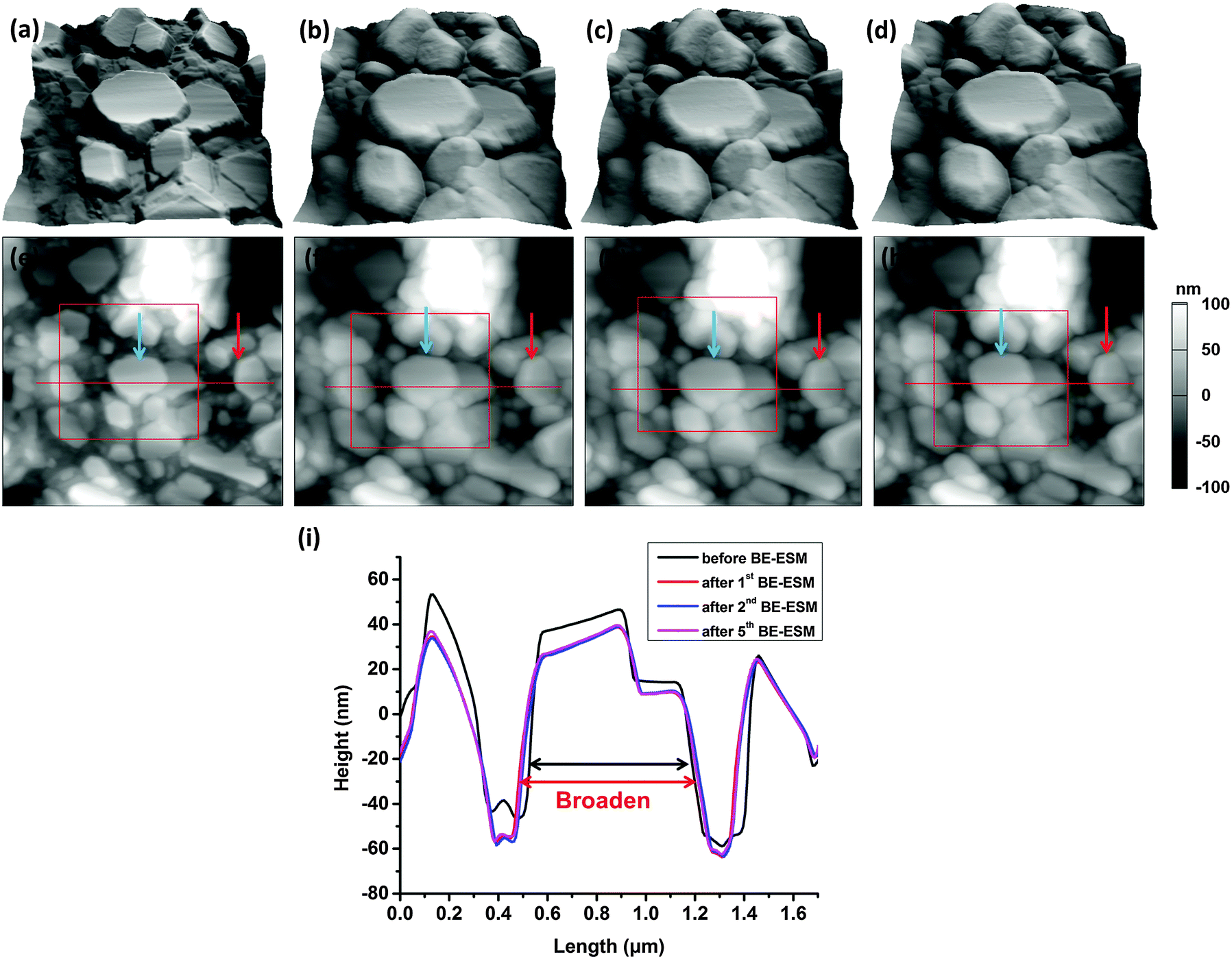 | ||
| Fig. 3 (a) to (d) are the 3D AFM height images at 1 × 1 μm2 area of the sample surface in Li1.2Co0.13Ni0.13Mn0.54O2 cathode film before, after 1st, 2nd and 5th BE-ESM images (with 3Vac bias); (e) to (h) are the corresponding AFM height images (2 × 2 μm2), in which the BE-ESM imaged area (red square) is located approximately at the centre of the region scanned by AFM; and (i) is the height profile along the lines in the images (e) to (h), respectively. All the AFM images were scanned by a pixel density of 256 × 256 and a scan rate of 1 Hz. | ||
It should be noted that the BE technique is not operated in a normal scanning mode. During the BE measurement, the SPM tip is fixed in one location and the frequency is swept with the pre-defined range, the tip is then lifted and moved to the next location to perform the same measurement. Such measurements will be performed in a grid matrix. Hence the tip wear in the BE technique is minimal. However, to exclude the possible effects of the tip change during BE imaging, a comparative AFM scanning with the tip was performed after BE imaging and a new tip is conducted over the same region. The topography images by using old and new tips show the same features (Fig. S3, ESI†), and this indicates that the grain expansion is a real phenomenon under external electric field and not an artifact caused by the tip wearing. The topography changes are caused by the Li-ion movements and redistribution under the electric field. When the cathode is biased, both ion-diffusion and ion-migration may be operated simultaneously, while after removing the bias, only ion-diffusion may be functioned.17 Therefore, the induced Li-ion movement outside the biased area is governed by the diffusion mechanism. In a layered structure cathode, the intercalation of Li-ions into cathode can cause an extension of the a-axis and contraction of the c-axis, while the de-intercalation of Li-ions out of the cathode can cause the inverse changes in the lattice parameter.33 Under the bias cycles, Li-ions diffuse in and out of the actuated grains, accompanied by volumetric expansion and reduction. The grain expansion (a-axis extension) indicates an increase of Li-ion concentration and Li-ions diffuse into this individual grain through a complicated boundary network. Due to the discrepant effect of oscillatory positive and negative bias, the intercalation/de-intercalation induced by the oscillatory bias cycle can be asymmetric, resulting in irreversible topography changes.
Fig. 4(a) to (c) are the 3D images of the resonance amplitude overlapped on the topographic images of the 1st, 2nd and 5th BE-ESM with the 3Vac bias in the same 1 × 1 μm2 region. In the BE-ESM measurements, the magnitude of electrochemical strain (amplitude) is proportional to the local electrochemical activity in a small volume of the material below the biased tip.18 The variations in the surface deformation can be caused by a number of factors: (i) the Li-ion concentration difference existing in different regions, higher electrochemical strain (larger deformation) represents higher Li-ion concentration; (ii) the heterogeneity and anisotropy of the sample surface caused by different grain structures. Li-ions are relatively easier to diffuse along preferred directions; as a result, Li-ion movement within the material is anisotropic; and (iii) the different crystallographic orientations of the grains under bias. For an actuated grain with c-axis aligned normally to the substrate, the detected deformation (or strain) is maximal because small amounts of Li-ion concentration variation can induce a large amount of c-axis fluctuation.34 However, this factor may be eliminated in this study as most of grains in the Li-rich cathode film are (003) oriented.
 | ||
| Fig. 4 BE-ESM images overlaid on topographic images (with 3Vac bias): (a) to (c) are the amplitude images obtained from the 1st, 2nd and 5th BE-ESM imaging, respectively; (d) to (f) are calculated diffusion coefficient maps, respectively; and (g) average diffusion coefficient vs. the number of BE-ESM images, and the error bars indicate the variation of the diffusion coefficient within the image. The BE-ESM images are obtained with a pixel density of 64 × 64 over 1 × 1 μm2. | ||
Fig. 3(c) and (d) show that after 2nd to 5th BE-ESM imaging, the grain size and morphology are fairly similar to those after the 1st BE-ESM imaging. From the line profile analysis [Fig. 3(i)], the height remains almost the same in the 2nd to 5th BE-ESM images. This suggests that the movement of certain Li-ions during 1st BE-ESM imaging may be irreversible, as these Li-ions cannot return to their previous positions after 1st BE-ESM imaging. On the other hand, Fig. 4(b) and (c) still show non-zero electrochemical strain. This indicates that certain bias-induced Li-ion movement still occurs during 2nd to 5th BE-ESM imaging. However, the movement of these Li-ions does not cause significant changes in the topographic image, suggesting reversible Li-ion movement. Hence, the bias-induced Li-ion redistribution is partially reversible in the Li-rich cathode film after the 1st BE-ESM image. Generally speaking, the strengths of the electrochemical strain from 1st to 5th BE-ESM images continually decrease [Fig. 4(a) to (c)]. The ESM amplitudes approximately approach to a value of ∼0.48 pm; this indicates there may be a concentration limit for reversibly movable Li-ions. Since BE-ESM is conducted at a high frequency regime, the dependence of electrochemical strain on the region of the tip–surface contact is generally weak.16 Therefore, the reduced amplitude response reveals that under repeated electric field, the electrochemical activity of Li-ions gradually attenuates.
Fig. 4(d) to (f) are 3D spatial maps of the calculated local diffusion coefficients (overlaid on topographic images) during the multiple BE-ESM imaging. As the number of the BE-ESM images increases, the diffusion coefficient reduces significantly. From the 1st to 5th BE-ESM images, the regions with higher diffusion coefficients (purple and green colour regions) reduce and the regions with lower diffusion coefficients (red and yellow colour regions) increase. The averaged diffusion coefficient across the imaged area can be extracted and fitted on a Gaussian-type plot. Fig. 4(g) shows the average diffusion coefficient and the standard deviation as a function of the numbers of the BE-ESM image. The local diffusion coefficients decrease continuously with the increase in number of BE-ESM images. In addition, the variation in the diffusion coefficient within one image is also reduced. The reasons for this are most likely the permanent trapping of Li-ions in grain structures, as well as the electrochemical fatigue and degradation under repeated electric field. Furthermore, the decrease of the local diffusivity value is more significant after the 1st imaging with the initial local diffusivity decreases by ∼45%, which is approximately 60% of the total loss of the local diffusivity in the material. From the perspective of battery cycling performance, the observed irreversible topography change and the diffusivity loss at the nanoscale can be correlated with each other to study the capacity loss of the Li-rich cathode materials at the device level.
In situ relaxation mapping due to diffusion
Fig. 5(a) and (b) show the AFM deflection image on an area of 1 × 1 μm2 of Li-rich thin film cathode before and after BE-ESM measurement with 3Vac. As the actuated grain is saturated with lithium, it is found that a higher bias is required to overcome the necessary chemical potential barrier to intercalate more Li-ions into the cathode layers.34 Therefore, the BE-ESM image with 4Vac is conducted on the same area, after which a series of continuous AFM scans (only the first four are shown here) are immediately conducted. The corresponding AFM images are shown in Fig. 5(c) to (f). After BE-ESM with a higher bias, most grains show a greater degree of expansion than that with 3Vac, as illustrated by grain G1 and G2 in Fig. 5(b) and (c). The extent of Li-ion movement within the thin film depends on the applied cyclic voltage. Higher voltage can cause larger changes in the Li-ion concentration under the SPM tip, resulting in more dramatic volumetric changes. Certain grains (marked by red arrow) show a slight decrease in the grain size. An interesting observation is that, during the third AFM image, grain contraction is observed, as illustrated by G1 and G2 in Fig. 5(e). At the same time, the grain marked by the red arrow expands slightly. The fourth scan shows only a little topography changes, as marked by a yellow arrow in Fig. 5(f). The topography remains the same after the fourth scan. The topography changes from Fig. 5(c) to (f) indicate a redistribution of Li-ions without the presence of an electric field. In addition, the time consumed for mode switching (from BE-ESM to AFM) and parameter adjustment is approximately 30 seconds. The time consumed for each AFM scan is about 4 minutes and 15 seconds. As shown in Fig. 5(g), the grain sizes of both grains (G1 and G2) decrease significantly with time, especially after 9 minutes. Here, the observed topography changes as time elapse (relaxation) is attributed to Li-ion diffusion. It should be noted that the degree of topography changes and relaxation time depend on the specific grain configuration and connectivity of the grain junction. The shrinkage of a grain (a-axis contraction) indicates a decrease in the amount of Li-ions in this individual grain, i.e., Li-ions are extracted out of this grain. If a grain is over-saturated with Li-ions, then a certain amount of Li-ions can release out to maintain stability of the grain structure, and this results in grain shrinkage. For the thin film cathode used here, the grains are connected and piled up layer by layer. However, the evolution of the lattice parameter due to the Li-ion intercalation/de-intercalation of the Li-rich cathode cannot be determined under current conditions. Therefore, it is not possible, at least for now, to quantity the exact amount of Li-ions inserting/extracting through grains from the information obtained by AFM images alone.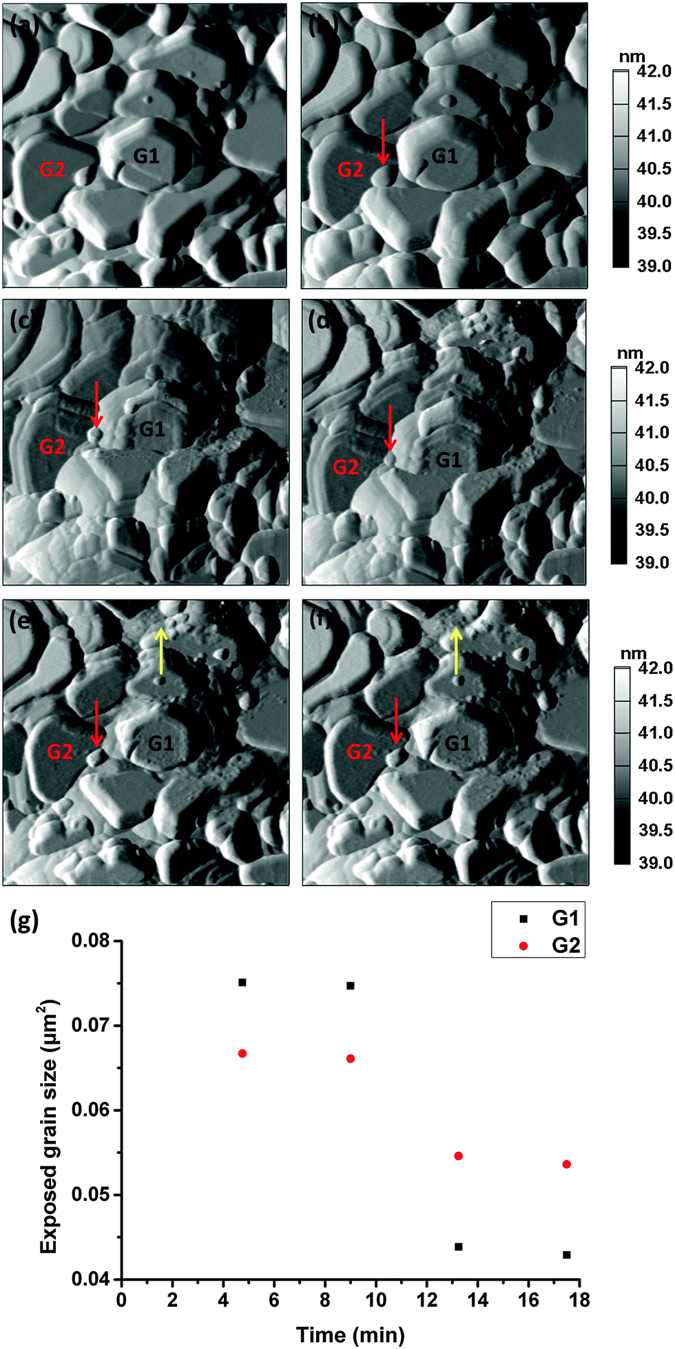 | ||
| Fig. 5 (a) and (b) are the AFM deflection images on an area of 1 × 1 μm2 of the Li-rich thin film cathode before and after BE-ESM measurement with 3Vac; (c) to (f) are four continuous AFM deflection images scanned immediately after a BE-ESM measurement with 4Vac; (g) grain size evolution as a function of time. All the AFM images were scanned by a pixel density of 256 × 256 and a scan rate of 1 Hz. | ||
Conclusions
In summary, this paper has presented the results of in situ studies on Li-ion diffusion at the nanoscale in Li-rich layered oxide cathode film using SPM techniques (BE-ESM and AFM). The results show that the local diffusion coefficients can be mapped from the ESM images. The topography changes due to Li-ion diffusion are observed and bias-induced Li-ion redistribution is partially reversible. Li-ion diffusivity attenuates gradually over several BE-ESM images and the loss is mainly during the first imaging. Furthermore, topography evolution as a function of time (relaxation) is observed. In addition, this work shows that the BE-ESM technique provides a powerful approach to induce the localized Li-ion movement at nano- to micro-scales. The results also demonstrate that by combining the AFM topography images with the electrochemical deformation from the BE-ESM images, the Li-ion diffusion behaviour can be studied. However, one of the limitations of the SPM technique is the lack of the chemical information on the materials, hence limiting the detailed physical chemistry oriented interpretations and visualization of Li-ion diffusion processes in the materials. However, the SPM technique can be used to detect the changes in the localized properties. In this sense, this method and analysis are suitable to study the changes in the various properties that the cathode materials undergo during the charge/discharge processes. In addition, this work also offers a fundamental understanding of the ion diffusion phenomena and underlying mechanisms in the cathode material under the electric field. In addition, this work also shows the significance of the SPM-based techniques to the Li-ion battery research; and the measurements developed in this research can also be extended to other oxide materials.Acknowledgements
This work is supported by Ministry of Education (Singapore) through the National University of Singapore under Academic Research Fund (R-265-000-406-112). One of the author (YS) would also like to thank the support of scholarship by the Ministry of Education (Singapore) under the Academic Research Fund (R-265-100-406-112).References
- A. Manthiram, J. Phys. Chem. Lett., 2011, 2, 176–184 CrossRef CAS.
- B. Scrosati and J. Garche, J. Power Sources, 2010, 195, 2419–2430 CrossRef CAS PubMed.
- J. M. Clark, S. Nishimura, A. Yamada and M. S. Islam, Angew. Chem., Int. Ed., 2012, 51, 13149–13153 CrossRef CAS PubMed.
- J. W. Fergus, J. Power Sources, 2010, 195, 939–954 CrossRef CAS PubMed.
- H. J. Yu and H. S. Zhou, J. Phys. Chem. Lett., 2013, 4, 1268–1280 CrossRef CAS.
- L. Li, K. S. Lee and L. Lu, Funct. Mater. Lett., 2014, 07, 1430002 CrossRef.
- Y. Wu and A. Manthiram, Electrochem. Solid-State Lett., 2006, 9, A221–A224 CrossRef CAS PubMed.
- W. C. West, J. Soler, M. C. Smart, B. V. Ratnakumar, S. Firdosy, V. Ravi, M. S. Anderson, J. Hrbacek, E. S. Lee and A. Manthiram, J. Electrochem. Soc., 2011, 158, A883–A889 CrossRef CAS PubMed.
- H. Koga, L. Croguennec, P. Mannessiez, M. Ménétrier, F. Weill, L. Bourgeois, M. Duttine, E. Suard and C. Delmas, J. Phys. Chem. C, 2012, 116, 13497–13506 CAS.
- S. H. Kang, P. Kempgens, S. Greenbaum, A. J. Kropf, K. Amine and M. M. Thackeray, J. Mater. Chem., 2007, 17, 2069–2077 RSC.
- J. Zhu, J. Feng, L. Lu and K. Zeng, J. Power Sources, 2012, 197, 224–230 CrossRef CAS PubMed.
- J. Zhu, K. Zeng and L. Lu, J. Appl. Phys., 2012, 111, 063723 CrossRef PubMed.
- X. J. Zhu, C. S. Ong, X. X. Xu, B. L. Hu, J. Shang, H. L. Yang, S. Katlakunta, Y. W. Liu, X. X. Chen, L. Pan, J. Ding and R. W. Li, Sci. Rep., 2013, 3, 1084 Search PubMed.
- N. Balke, S. Jesse, A. N. Morozovska, E. Eliseev, D. W. Chung, Y. Kim, L. Adamczyk, R. E. Garcia, N. Dudney and S. V. Kalinin, Nat. Nanotechnol., 2010, 5, 749–754 CrossRef CAS PubMed.
- N. Balke, S. Jesse, Y. Kim, L. Adamczyk, A. Tselev, I. N. Ivanov, N. J. Dudney and S. V. Kalinin, Nano Lett., 2010, 10, 3420–3425 CrossRef CAS PubMed.
- A. N. Morozovska, E. A. Eliseev, N. Balke and S. V. Kalinin, J. Appl. Phys., 2010, 108, 053712 CrossRef PubMed.
- S. Jesse, N. Balke, E. Eliseev, A. Tselev, N. J. Dudney, A. N. Morozovska and S. V. Kalinin, ACS Nano, 2011, 5, 9682–9695 CrossRef CAS PubMed.
- S. Jesse, A. Kumar, T. M. Arruda, Y. Kim, S. V. Kalinin and F. Ciucci, MRS Bull., 2012, 37, 651–658 CrossRef CAS.
- N. Balke, E. A. Eliseev, S. Jesse, S. Kalnaus, C. Daniel, N. J. Dudney, A. N. Morozovska and S. V. Kalinin, J. Appl. Phys., 2012, 112, 052020 CrossRef PubMed.
- Q. N. Chen, Y. Y. Liu, Y. M. Liu, S. H. Xie, G. Z. Cao and J. Y. Li, Appl. Phys. Lett., 2012, 101, 063901 CrossRef PubMed.
- J. Zhu, L. Lu and K. Zeng, ACS Nano, 2013, 7, 1666–1675 CrossRef CAS PubMed.
- S. Jesse and S. V. Kalinin, J. Phys. D: Appl. Phys., 2011, 44, 464006 CrossRef.
- S. Jesse, S. V. Kalinin, R. Proksch, A. P. Baddorf and B. J. Rodriguez, Nanotechnology, 2007, 18, 435503 CrossRef.
- M. P. Nikiforov, S. Jesse, A. N. Morozovska, E. A. Eliseev, L. T. Germinario and S. V. Kalinin, Nanotechnology, 2009, 20, 395709 CrossRef CAS PubMed.
- B. Yan, J. Liu, B. Song, P. Xiao and L. Lu, Sci. Rep., 2013, 3, 3332 Search PubMed.
- J. B. Bates, N. J. Dudney, B. J. Neudecker, F. X. Hart, H. P. Jun and S. A. Hackney, J. Electrochem. Soc., 2000, 147, 59–70 CrossRef CAS PubMed.
- H. Xia and L. Lu, Electrochim. Acta, 2007, 52, 7014–7021 CrossRef CAS PubMed.
- H. Katsui, Y. Yamashita, R. Tu and T. Goto, J. Ceram. Soc. Jpn., 2013, 121, 406–410 CrossRef CAS.
- P. J. Bouwman, B. A. Boukamp, H. J. M. Bouwmeester and P. H. L. Notten, J. Electrochem. Soc., 2002, 149, A699–A709 CrossRef CAS PubMed.
- P. J. Bouwman, B. A. Boukamp, H. J. M. Bouwmeester, H. J. Wondergem and P. H. L. Notten, J. Electrochem. Soc., 2001, 148, A311–A317 CrossRef CAS PubMed.
- A. Suzuki and Y. Mishin, J. Mater. Sci., 2005, 40, 3155–3161 CrossRef CAS.
- N. Balke, S. Kalnaus, N. J. Dudney, C. Daniel, S. Jesse and S. V. Kalinin, Nano Lett., 2012, 12, 3399–3403 CrossRef CAS PubMed.
- A. Clémençon, A. T. Appapillai, S. Kumar and Y. Shao-Horn, Electrochim. Acta, 2007, 52, 4572–4580 CrossRef PubMed.
- D. Chung, N. Balke, S. V. Kalinin and R. E. Garcia, J. Electrochem. Soc., 2011, 158, A1083–A1089 CrossRef CAS PubMed.
Footnote |
| † Electronic supplementary information (ESI) available: XRD patterns of Li1.2Co0.13Ni0.13Mn0.54O2 thin film and AFM topographic images show grains with (003) orientation and well-defined hexagon-like geometry. The chemical diffusion coefficient of Li vs. potential during the charge state in Li-rich cathode film determined by PITT experiments. The AFM topographic images obtained by using the tip after BE-ESM imaging and a new tip on the same area. See DOI: 10.1039/c5cp01999k |
| This journal is © the Owner Societies 2015 |