
 Open Access Article
 This Open Access Article is licensed under a Creative Commons Attribution-Non Commercial 3.0 Unported Licence
Electrochemical behavior of thin-film Sm-doped ceria: insights from the point-contact configuration
Tae-Sik
Oh†
and
Sossina M.
Haile‡
*
California Institute of Technology, Materials Science, Pasadena, California, USA. E-mail: smhaile@caltech.edu; sossina.haile@northwestern.edu
First published on 21st April 2015
Abstract
The electrochemical behavior of chemical vapor deposition (CVD) grown porous films of Sm-doped ceria (SDC) for hydrogen oxidation has been evaluated by impedance spectroscopy using a point contact geometry at a temperature of 650 °C. Porous SDC films, 950 nm in thickness, were deposited on both sides of single-crystal YSZ(100). Pt paste was applied over the surface of one SDC layer to create a high-activity counter electrode. Ni wire was contacted to the surface of the other SDC layer to create a limited contact-area working electrode. The active area of contact at the working electrode was determined using the Newman equation and the electrolyte constriction impedance. The radius of this area varied from 5 to 18 μm, depending on gas composition and bias. The area-normalized electrode impedance (where the area was that determined as described above) varied from 0.03 to 0.17 Ω cm2 and generally decreased with cathodic bias and decreasing oxygen partial pressure. From an analysis of the dimensions of the active area with bias, it was found that the majority of the overpotential occurred at the SDC|gas interface rather than the SDC|YSZ interface. Overall, the anode overpotential is found to be extremely small, competitive with the best oxide anodes reported in the literature. Nevertheless, the impedance falls in line with expected values based on extrapolations of the properties of dense, flat SDC model electrodes grown by pulsed laser deposition (Chueh et al., Nat. Mater., 2012). The results demonstrate that, with suitable fabrication approaches, exceptional activity can be achieved with SDC for hydrogen electrooxidation even in the absence of metal–oxide–gas triple phase boundaries.
1. Introduction
As a result of its high ionic conductivity, acceptor doped ceria is a promising solid oxide fuel cell (SOFC) electrolyte material for intermediate temperature operation, 500–800 °C. The consideration of ceria as a fuel cell electrolyte has been accompanied by its evaluation as a component in a composite anode, typically alongside Ni as the metallic counterpart. Most studies have generally shown that introduction of ceria into metal–ceramic composite anodes enhances hydrogen electrooxidation activity.1 The improvement is attributed not only to the higher ionic conductivity of the electrolyte component relative to yttria stabilized zirconia (YSZ), but also to the inherent electrochemical activity of ceria.2 Despite the rising interest in ceria, comprehensive studies of its polarization behavior, away from zero bias, are limited. The handful of studies which have appeared in the literature3–8 employed high temperatures (700 to 900 °C) and thus do not address modern goals of intermediate temperature operation that would lower the cost and increase the lifetime of SOFCs.9 In prior work we established that columnar porous films of samaria-doped ceria (SDC) films, grown by pulsed laser deposition onto yttria stabilized zirconia, display extremely low electrode resistance for the hydrogen electrochemical oxidation reaction at the attractive temperature of 650 °C;10 for example, the area specific electrode resistance for a 4.4 μm film was found to be just 0.24 Ω cm2 (for the time = 0 measurement under 2% H2O, balance H2). However, those measurements, like the majority of electrode studies, were limited to small perturbation, zero-bias conditions. Here, we explicitly address polarization behavior of porous ceria under bias. In contrast to our earlier work, however, we employ chemical vapor deposition for film growth because of the greater suitability of this fabrication route to eventual implementation in commercial devices.Polarization characteristics are most often measured using a reference electrode. However, as widely appreciated, proper positioning of this electrode is critical in solid state systems, and even slight misalignment can result in significant experimental artifacts.11,12 Although correction procedures are available,13 in order to entirely circumvent such difficulties we employ here a referenceless geometry in which the working electrode has a much smaller area than the counter electrode. Under suitable conditions this geometry leads to negligible potential drop at the counter electrode relative to that at the working electrode.14 Thus, the electrode impedance measured by impedance spectroscopy will be dominated by that of the working electrode. Similarly, any applied bias will result in negligible potential drop at the counter electrode, enabling determination of the potential drop at the working electrode. The point-contact geometry has some precedence in SOFC electrode studies,15–17 but, to the best of our knowledge, with the exception of a preliminary study by Mogensen and coworkers18 has not been employed to probe behavior under bias.
2. Sample preparation and physical characteristics
The overall cell configuration employed in this study is shown in Fig. 1. Both the counter and working electrocatalysts are porous SDC (samarium doped ceria), covering the entirety of both sides of a 0.5 mm thick YSZ(100) single crystal substrate (MTI Corp, 1 cm × 1 cm in area). The asymmetric geometry was achieved by applying a current collector over the entire area of one electrocatalyst layer, to form the counter electrode, and making point contact to the other electrocatalyst layer using Ni wire, to form the working electrode. The porous SDC layers were grown by chemical vapor deposition, using in an in-house constructed vertical cold-wall reactor.19 Two commercially available metal–organic sources were employed as-received: Ce(tmhd)4 (Strem Chemicals, CAS#: 18960-54-8, 99.9% cation purity) and Sm(tmhd)3 (Strem Chemicals, CAS#: 15492-50-9, 99.9% cation purity). These precursors were vaporized in dedicated separate evaporators using Ar as a carrier gas, following a procedure developed specifically for solid precursors such as these.20 The Sm concentration in the deposited film was controlled by independently manipulating the precursor evaporation temperatures. Oxygen was supplied separately to the deposition chamber to ensure complete decomposition of the organics at the growth temperature of 600 °C. The growth time was fixed at 60 min to achieve a film thickness of ∼950 nm, as determined by cross-sectional scanning electron microscopy (SEM). Complete deposition conditions are summarized in Table 1. | ||
| Fig. 1 Schematic rendition of the asymmetric cell. Not to scale. | ||
| Substrate | YSZ(100), 0.5 mm thick |
|---|---|
| Growth temperature (°C) | 600 |
| Growth pressure (Torr) | 3 |
| Growth time (min) | 60 |
| Gas flow rate (sccm) | Sm carrier gas (Ar):50 |
| Ce carrier gas (Ar):50 | |
| Oxygen:50 | |
| Ce precursor evaporation temperature (°C) | 190 |
| Sm precursor evaporation temperature (°C) | 130 |
The electrochemical cell was fabricated by first growing the counter electrode catalyst layer and then applying to this layer the Pt current collector. Specifically, Pt paint (Engelhard 6082) was brush-coated over the entirety of the oxide film and fired to burn off organics (900 °C, 2 h). The resultant porous platinum layer had good adhesion to the underlying oxide. The working electrocatalyst layer was then grown on the other side of the substrate. Point contact to this layer was made using a nickel wire (254 μm diameter, Espi Metals, Knc1225) which was bent into a U shape and used to hold the sample firmly in place.21
SEM images were collected using a JEOL 7500F HRSEM operating at 5 kV acceleration voltage. Elemental analysis was performed using an energy dispersive X-ray spectroscopy system (EDS, INCA by Oxford) integrated with this SEM, with the electron beam voltage set at 15 keV. Dopant concentration was determined by averaging over several randomly selected spots. X-ray diffraction patterns were collected with Cu Kα radiation in the Bragg–Brentano geometry (Rigaku Hyperglex, 40 kV, 30 mA).
The as-grown films were found to display a columnar morphology, as evident from the electron microscopy images, Fig. 2a and b. The images collected after the completion of the electrochemical measurements, Fig. 2c and d, show that prolonged exposure (>350 h) to high temperature caused the structure to coarsen and sinter. However, some porosity extending through the entire thickness persists (as reflected in the roughness of the cross-sectional fracture surface), and the grain size remains too small for easy resolution. The X-ray diffraction pattern of the film collected after electrochemical measurement, Fig. 3, reveals that, as observed previously for CVD grown ceria,21 the film has a (100) preferred orientation, consistent with the (100) orientation of the YSZ substrate. In particular, the relative intensity of the (200) to (111) diffraction peak is 8.5 for the film, many times greater than the value of ∼0.3 expected for a sample with random crystallite orientation. It is noteworthy that this preferred orientation is retained even after high-temperature electrochemical characterization. From the broadening of the (200) peak, the average grain size (in the film thickness direction) was found, using the Scherrer equation22 after accounting for instrument broadening, to be 26 nm. This small size is consistent with the fine features evident in the electron micrographs. The chemical composition of the film was found to be Sm0.06Ce0.94O1.97−δ. The Zr signal detected from the substrate was ignored in the analysis of the film stoichiometry.
 | ||
| Fig. 2 Scanning electron micrographs of CVD grown films. (a) And (b) are top down and cross-sectional images, respectively, of a representative as-grown film; (c) and (d) are top-down and cross-sectional images respectively, of the film used for electrochemical studies, after completion of the electrochemical characterization. | ||
 | ||
| Fig. 3 XRD pattern of the Sm doped ceria film after electrochemical characterization. | ||
3. Electrochemical measurements
3.1 Experimental details
Before introducing the electrochemical measurement methods and results, it is of value to consider the maximum allowable size of the working electrode to achieve an electrode response that has negligible contribution from the counter electrode. Based on the analysis of Sasaki et al.,14 the working electrode will be responsible for >99% of the sum of the electrode responses when the working electrode has a radius that is less than 10% of that of the effective counter electrode, where the latter is the region through which current passes as a result of the current spreading. The effective radius of the counter electrode, reffCE, is given by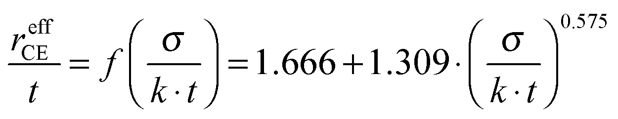 | (1) |
 | ||
| Fig. 4 SEM image of a scratch made by the nickel wire electrode on the Sm doped ceria thin film. | ||
The entire asymmetric cell was exposed to a uniform gas atmosphere that was controlled by mixing moist H2, humidified by passing through a bubbler held at 65 °C, dry H2, and dry Argon. Three mass flow controllers were used to set the respective flow rates while keeping the total flow rate at 101 sccm. Four gas conditions (A–D) were examined, as listed in Table 2, where the reported H2O partial pressure is based on an assumption of full saturation of the moist H2, and the O2 partial pressure is computed assuming equilibrium between H2, H2O and O2. All electrochemical measurements were made at 650 °C, with a K-type thermocouple placed in close proximity to the working electrode (within 1 cm). Impedance data were collected using a Solartron 1260 with an excitation voltage amplitude of 20 mV over the frequency range 10 MHz to 5 mHz (48 data points). Both zero-bias and DC biased measurements were performed as described in detail below. Analysis of the impedance data was performed using the commercial software package ZView (Scribner Associates).
| Condition | pH2 (atm) | pH2O (atm) | pO2 (atm) |
|---|---|---|---|
| A | 0.036 | 0.12 | 5.4 × 10⁻²² |
| B | 0.039 | 0.016 | 8.5 × 10⁻²⁴ |
| C | 0.40 | 0.12 | 4.3 × 10⁻²⁴ |
| D | 0.44 | 0.016 | 6.8 × 10⁻²⁶ |
To minimize the possibility of thermomechanical evolution during electrochemical measurement, the sample was thermally cycled 9 times from room temperature to temperatures between 600 °C and 800 °C (heating/cooling rate = 3 °C min−1) before evaluation. While this treatment helped minimize changes in impedance response over time, temporal evolution was not completely eliminated. Specifically, the absolute impedance increased by a factor of about 2.5 between the first and final measurements, which took place over a period of more than 300 h. Accordingly, comparisons presented below within individual figures to demonstrate the influence of parameters generally show spectra collected in close temporal proximity, but comparisons between figures are less meaningful.
3.2 Features of the electrochemical response
A representative impedance spectrum under zero bias and gas condition A is presented in Fig. 5 in the complex plane (−Zimagvs. Zreal as parametric functions of ω). Two highly symmetric arcs, almost perfectly centered on the real axis, are evident, and the high frequency arc is slightly offset from the origin (not visible on the scale presented). The small offset resistance is attributed to the (conventional) impedance of the substrate and additional ohmic resistances. At 650 °C the YSZ substrate is expected to contribute ∼6 Ω of resistance.23 While this is somewhat smaller than the 47 Ω offset resistance observed, it is several orders of magnitude smaller than the diameters of either of the two impedance arcs, indicating these features cannot be due simply to the YSZ. Furthermore, the relative dielectric constant of YSZ at 650 °C is ∼60,25 implying a bulk characteristic frequency of ∼1.5 GHz. As this exceeds the highest measurement frequency, it is to be expected the bulk impedance arc has not been captured, and instead yields the observed high frequency offset.
 | ||
| Fig. 5 A representative Nyquist plot of impedance measured under zero bias and gas condition A (Table 2). | ||
Turning to the main features in the impedance spectrum, the high frequency arc is attributed to a constriction effect involving the properties of both the electrolyte and the electrocatalyst layer. It is proposed that electrical constriction effects occur in the geometry of Fig. 1 because the field lines behave differently at high and low frequencies. Specifically, at high frequencies, the highly mobile electrons in the ceria film can presumably respond such that the electric field lines access the entirety of the YSZ substrate. At low frequencies, however, the electron flux is expected to be limited by the electrochemical reaction at the point contact, and thus the field lines at the working electrode will be restricted to the contact region. The consequence is that the magnitude of the impedance increases with decreasing frequency, giving rise to the observed high frequency arc. Constriction effects are relatively common in solid-state electrochemical systems26,27 and have been observed in particular in the study of porous ceria electrocatalyst layers in conjunction with geometrically restricted current collectors.24 Thus, it is not surprising that such a feature appears here. With this assignment, it is then expected that the in-plane electronic resistance of the ceria film contributes to the high-frequency offset and explains its high value relative to the resistance of YSZ. The remaining feature, the low-frequency arc, is attributed to the impedance of the electrochemical reaction occurring in the electrochemically active region, in the vicinity of the Ni working electrode. Validation of this assignment, by comparison of either the resistance or capacitance of this response to reported values for ceria, requires knowledge of the active area of the electrode, a task undertaken below.
Based on the visual appearance of the spectra, the data were modeled according to an equivalent circuit with topology R(RQ)(RQ), where R is a resistor of impedance ZR = R, and Q is a constant phase element of impedance ZQ = Q0−1(iω)−n, in which Q0 is a constant, ω is angular frequency, and n is a constant between 0 and 1 reflecting the dispersion in electrochemical behavior.28 In all cases n was found to be greater than 0.8 and the equivalent capacitance from the constant phase element was computed according to C = Q1/n0R(1/n−1), applicable when n is close to 1.
Taking the real component of the impedance at the low frequency limit of the constriction response to represent the resistance through the electrolyte in contact with a point electrode, Rpoint, it is possible to estimate the diameter of the contact region. Specifically, Newman has shown that the resistance measured across an infinitely thick electrolyte placed in contact with a point-electrode of diameter D is given by29
 | (2) |
With these approximations, the contact diameter computed for the conditions of Fig. 5 is ∼8.3 μm, a distance that is slightly larger than the width of the scratch mark in Fig. 4 and thus one that is immediately plausible. The dimensionless length, D/πt, is 0.005, substantially below 1 as required for applicability of the Newman equation. In our earlier study of model ceria electrodes, in which the ceria was deposited on YSZ as a dense, flat film, placement of metal electrodes as far apart as 80 μm was possible without detrimental impact on activity.2 The much smaller active area in the present study likely reflects poor electronic in-plane conductivity across the internal boundaries of the columnar structure. Based on the estimated active diameter, the area-specific electrode resistance of the CVD porous film is 0.048 Ω cm2. This value is a full order of magnitude smaller than the value of Jung et al. referenced above for porous, columnar PLD ceria films extrapolated to similar measurement conditions (∼0.6 Ω cm2).24 While surprising at first glance, it is noteworthy that the activity of the columnar PLD ceria was lower than anticipated on the basis of the measurement of dense ceria films also grown by PLD methods;2 the high activity obtained here is, in fact, quite satisfactory when compared to the behavior of those model electrodes.
The capacitance associated with the electrochemical reaction response is 7.0 × 10⁻⁸ F, implying area and volume specific values of 0.13 F cm−2 and 1400 F cm−3, respectively. This very large capacitance is taken to be the sum of contributions from the chemical capacitance and interfacial capacitance, the latter at the ceria–gas interface. A bulk dense film of SDC is expected to display a chemical capacitance of ∼250 F cm−3 (ref. 30) under the measurement conditions of Fig. 5, and, as such, can only account for a fraction of the observed capacitance. Indeed, if the film is taken to be roughly 80% dense, 1200 F cm−3 of capacitance must be due to the interfacial effects. In the case of PLD grown porous films (∼35% porous) measured under similar conditions, interfacial effects also dominated the total capacitance, but in that case contributed ∼280 F cm−3. A factor of 4–5 difference in the surface capacitance for SDC films grown under different conditions using different systems and presumably presenting different volume-specific surface areas is not inherently surprising. Indeed, given the order of magnitude differences in electrochemical reactivity at the surfaces of the CVD and PLD grown films, greater agreement in the capacitance values would be unexpected. In sum, all quantities are consistent with the assignment of the high frequency arc to constriction effects and the low frequency arc to the electrochemical reaction impedance at the ceria–gas interface, and with the use of the Newman formalism for determining the electrochemically active area.
The influence of gas composition and of bias on the impedance response is presented in Fig. 6. In Fig. 6(a) spectra collected under zero bias but at the four different gas conditions of Table 1 are shown. Analogously, the spectra presented in Fig. 6(b) were collected at several bias values, but all under gas condition A. For the latter, the measurements were made over the bias range ±200 mV in increments of 50 mV. The sample was allowed to equilibrate at each bias step (12 min hold followed by 12 min data acquisition) and, to avoid cumulative polarization effects, the voltage was returned to 0 for several minutes before stepping to the next higher voltage value. The measurement sequence was as follows: 0 V → anodic (+) bias (thick lines) → 0 V → cathodic (−) bias, (thin lines) → 0 V. This sequence was completed for each gas composition before moving on to the next (in the sequence B → A → C → D). The spectra presented in Fig. 6(a) are the zero bias measurements obtained after completing the anodic bias portion of each measurement, and they are generally equivalent to the average of the three zero bias measurements.
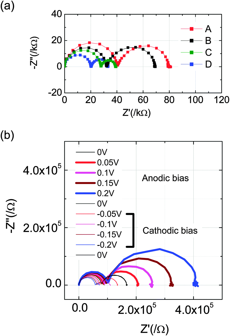 | ||
| Fig. 6 Impedance spectra collected (a) at the four gas conditions of Table 2 as indicated and zero bias, and (b) under gas condition A and applied bias as indicated. The measurements in (b) were performed in sequence as indicated in the legend (i.e., anodic bias first then cathodic). | ||
A significant feature of the spectra of in Fig. 6 is that each has two arcs regardless of gas atmosphere or bias voltage. Furthermore, the magnitude of the impedance (as reflected in the diameter of the arcs) clearly changes in response to either gas condition or bias. Specifically, a reduction in gas-phase oxygen partial pressure or an application of negative bias causes both impedance features to shrink. The first effect, a decrease in impedance with a decrease in oxygen partial pressure, is readily understood. The electronic conductivity of ceria increases under reducing conditions,31 and such a change can be expected to increase the size of the electrochemically active zone. This would, in turn, decrease the constriction resistance and, even for given electrochemical activity, the larger area would decrease the absolute resistance associated with the electrochemical reaction resistance. Beyond this effect, the activity of ceria is known to increase under more reducing conditions,31,32 serving as an additional reason for the decrease in the resistance associated with the low frequency arc. The change in behavior under bias has somewhat more subtle origins, but is also readily explained. Under negative (cathodic) bias, electrons are delivered to the working electrode, effectively reducing it. Thus, the behavior under cathodic bias is qualitatively similar to that under gas-phase induced reduction. It is noteworthy that in the example shown in Fig. 6(b) (but not all cases) the three zero bias spectra are coincident with one another.
For further analysis of the behavior of the working electrode, the electrode overpotential, η, is computed from knowledge of the current, I, at a given bias and recognition that, despite constriction effects, the electrolyte remains ohmic in its physical behavior. Thus
| η = ΔV − IRpoint | (3) |
3.3 Evaluation of the electrochemical active region
The constriction behavior is summarized in Fig. 7. In Fig. 7(a) is shown the area of the electrochemical active region determined from the impedance measurements under bias and at the four atmosphere conditions examined, as determined using eqn (2). Consistent with the raw impedance data, Fig. 6, it is evident that the area increases under more reducing gas-phase conditions and more negative bias. As noted, the application of bias effectively changes the oxygen chemical potential of the electrocatalytic ceria relative to that in the gas phase. The outlying data-points, collected under gas condition D and the largest cathodic biases, correspond to the most reducing conditions examined. As evidenced by a difference in zero-bias impedance spectra before and after polarization (not shown), these conditions triggered an irreversible, detrimental change in the cell properties, potentially due to the chemical expansion of ceria. Such behavior contrasts that observed in some perovskite-structured mixed-conducting cathodes that undergo bias-induced activation, enhancing the electrochemical reaction rate, after application of very large (as much as 5 V) bias.33 | ||
| Fig. 7 Influence of bias voltage on electrochemically active region and oxygen chemical potential in the electrocatalyst: (a) variation of active area with bias at the gas conditions of Table 2; (b) schematic of oxygen chemical potential profile across the electrocatalyst layer for a given value of the allocation factor, λ, and (c) variation of active area with computed equivalent oxygen partial pressure in the electrocatalyst taking λ = 0.8 (eqn (6)). | ||
It can be anticipated that the change in active area with bias is connected to changes in chemical potential in the electrocatalyst film. This potential in turn depends on the electrical potential profile. If the entirety of the potential drop between the Ni point electrode and the YSZ electrolyte were to occur at the ceria|gas interface, Fig. 7(b), black curve, with no potential drop at the YSZ|ceria interface, the oxygen chemical potential in the ceria would be given by
| μceriaO = μgasO + 2Fη | (4) |
| μceriaO = μgasO + λ2Fη | (5) |
 | (6) |
If one presumes that the area of the electroactive region is determined by the value of the electronic conductivity of the electrocatalyst, in turn set by its mean oxygen chemical potential, then one can immediately conclude from the fact that the area changes with overpotential, that λ is not zero (i.e., μceriaO ≠ μgasO). Replotting the area values against μceriaO with λ = 1, however, (not shown) does not result in overlap of the area values, indicating that the limit expressed in eqn (4) is not applicable either. Shown in Fig. 7(c) are the electroactive areas as a function of equivalent oxygen partial pressure in the electrocatalyst with λ = 0.8. This optimized value results in a striking alignment of the active areas across the four sets of measurements.
The slope in Fig. 7c, a double-logarithmic plot, is surprisingly shallow, just −1/6. If the analysis is correct, this weak dependence indicates that the diameter of the electrochemical active region (with a power law dependence on pO2 of −1/12) does not directly scale with the electronic conductivity. The latter displays a well-known −1/4 power law dependence on oxygen partial pressure.31 Nevertheless, the increase in area with decreasing pO2 and hence increasing electronic conductivity is clear. Accordingly, we propose that the extent of the electrochemical active regime is a function of the electronic conductivity of the electrocatalyst and that rapid electrochemical reaction at the ceria–zirconia interface results in an effective oxygen partial pressure in the ceria that is closer to the value in the YSZ electrolyte than it is to the value in the gas phase. This interpretation implies that the electrochemical reaction at the SDC–gas interface is rate-limiting, as might be expected. The true potential profile, however, is certainly more complex than the schematic illustration of Fig. 7(b) and likely includes potential drops at both interfaces. The electrode resistance extracted from the impedance spectra is taken to be a lumped electrochemical reaction resistance. Possible contributions to this resistance due to migration effects (ion, electron or gas-phase) are ruled out on the basis of previous studies2,10,24,34 and the relatively high mass flow rates employed.
Evaluation of the capacitance, specifically that corresponding to the low-frequency response, and its variation with pO2 and bias, provides a means of cross-validating the above interpretation. This capacitance increases dramatically in absolute value with decreasing gas-phase oxygen partial pressure, from about 2.82 × 10⁻⁷ F for gas condition A to 1.25 × 10⁻⁵ F for gas condition D. Such behavior has several possible sources and can be attributed to the increase in area (which is larger by about a factor of 4 for gas condition D), an increase in chemical capacitance under the more reducing conditions, and/or changes in surface dielectric properties. On a projected-area normalized basis (taking the effective area determined as described above) the capacitance increases from 0.14 to 1.56 F cm−2, indicating that area effects alone cannot explain the observed increase (otherwise, area normalization would yield a fixed value). The bulk chemical capacitance is expected to differ by an order of magnitude between the two gas conditions.30 However, as discussed above, the absolute magnitude of the chemical capacitance is computed to be a fraction of these values. Hence, the variation in area normalized chemical capacitance is likely to be due, in large part, to changes in the dielectric properties of the ceria–gas interface. While intriguing, a detailed investigation of capacitance effects is beyond the scope of the present study. Of significance here is that the capacitance behavior (showing a strong increase with reducing conditions) is consistent with a response associated with electrochemical reaction at the ceria surface.
3.4 Dependence of electrochemical activity on measurement conditions
The influence of gas atmosphere (under zero bias) and of bias (under gas condition A) on the electrochemical reaction resistance,![[R with combining tilde]](https://www.rsc.org/images/entities/i_char_0052_0303.gif) rxn, is shown Fig. 8, where the data are normalized according to the Newman active area. For clarity, the ohmic and constriction impedances have been removed from the data. In Fig. 8(b), line thickness indicates the magnitude of the bias. From Fig. 8(a) it is evident that rxn does not trend monotonically with oxygen partial pressure (unlike the result prior to area normalization, Fig. 6(a). This strongly indicates that pO2 (or, equivalently, electron concentration) is not the sole predictor of electrochemical activity in this films, in contrast to the behavior of free-standing polycrystalline SDC.32,35 Apparently, for these columnar films, H2 or H2O gas concentrations may be independently important in establishing the surface reaction rate. Alternatively, the area normalization may not be entirely appropriate because the Newman approach gives the area through which current flows at the SDC|YSZ interface, whereas the behavior of the field lines through the SDC may be rather complex and lead to a non-monotonic relationship between the active SDC surface area in the porous structure and the constriction area at the SDC|YSZ interface. In contrast, the results of Fig. 8(b) show an entirely monotonic dependence of electrode impedance on bias. However, for as-yet unknown reasons, bias induces a change in the shape of the electrode arc, with a small additional feature even appearing at low frequencies for large cathodic bias. For the purposes of this analysis, in which the overall magnitude of the electrode resistance is of the greatest interest, we simply evaluate the real value of impedance in the low frequency limit.
rxn, is shown Fig. 8, where the data are normalized according to the Newman active area. For clarity, the ohmic and constriction impedances have been removed from the data. In Fig. 8(b), line thickness indicates the magnitude of the bias. From Fig. 8(a) it is evident that rxn does not trend monotonically with oxygen partial pressure (unlike the result prior to area normalization, Fig. 6(a). This strongly indicates that pO2 (or, equivalently, electron concentration) is not the sole predictor of electrochemical activity in this films, in contrast to the behavior of free-standing polycrystalline SDC.32,35 Apparently, for these columnar films, H2 or H2O gas concentrations may be independently important in establishing the surface reaction rate. Alternatively, the area normalization may not be entirely appropriate because the Newman approach gives the area through which current flows at the SDC|YSZ interface, whereas the behavior of the field lines through the SDC may be rather complex and lead to a non-monotonic relationship between the active SDC surface area in the porous structure and the constriction area at the SDC|YSZ interface. In contrast, the results of Fig. 8(b) show an entirely monotonic dependence of electrode impedance on bias. However, for as-yet unknown reasons, bias induces a change in the shape of the electrode arc, with a small additional feature even appearing at low frequencies for large cathodic bias. For the purposes of this analysis, in which the overall magnitude of the electrode resistance is of the greatest interest, we simply evaluate the real value of impedance in the low frequency limit.
 | ||
| Fig. 8 Area normalized impedance spectra for the electrochemical reaction response (a) superposed for different pO2 under zero bias (from Fig. 6a), and (b) superposed for various biases under gas condition A (from Fig. 6b). | ||
The dependence of the electrode area-normalized impedance on overpotential and gas phase condition is summarized in Fig. 9. A subset of the results of Fig. 9 are presented in Fig. 10, in a format in which the influence of the gas composition is emphasized. Several features are noteworthy. First, as already noted in the discussion surrounding Fig. 5, the area-specific electrode resistance values extracted from this analysis are, at first glance, rather small, ranging from 0.03 to 0.17 Ω cm2. However, if one extrapolates from the conditions used to evaluate dense SDC,2 one expects rxn values in the range of 1 to 6 Ω cm2, even for a flat film. If the true surface area is just a factor of ∼30 larger than the projected area, then the observed resistance values would be achieved. Table 3 provides a detailed comparison of the expected and actual values under zero bias for the four gas conditions. The ratio between the extrapolated rxn(flat) and rxn determined here is a measure of the required surface area enhancement factor to explain the observed results. Even the largest value, of about 50, is not an unreasonable enhancement factor if one considers the difference in true surface area between that of a flat surface and that of a porous, columnar film.
 | ||
| Fig. 9 Variation in the area-specific electrochemical reaction resistance with overpotential under various gas conditions (Table 1). | ||
 | ||
| Fig. 10 3-Dimensional rendition of the dependence of area-specific electrochemical reaction resistance on gas condition and bias. The elevation of the point reflects the magnitude of the resistance, the size of the data point reflects the magnitude of the electrode overpotential, with cathodic shown in red and anodic in blue. | ||
| Condition | A | B | C | D |
|---|---|---|---|---|
| R(extr), Ω cm2 | 2.9 | 6.2 | 1.1 | 2.4 |
| R(meas), Ω cm2 | 0.08 | 0.12 | 0.05 | 0.11 |
| Ratio | 37 | 52 | 23 | 21 |
A second important feature (and one also briefly addressed above) is the absence of any trend in rxn with oxygen partial pressure. While, as already noted, oxygen chemical potential has been identified as the critical factor in some measurements of electrochemical activity on SDC under reducing conditions,31,32,36 the results in Table 3 demonstrate that in other instances the concentrations of other gaseous species are more important. Indeed, the analysis indicates that the decrease in absolute electrode impedance evident in Fig. 6a is driven more by the increase in electroactive area than a change in inherent activity in response to changes in gas species concentrations.
Perhaps the most important feature of the data in Fig. 9 is the largely monotonic behavior of rxn with bias. Specifically, rxn decreases under cathodic bias and increases when the bias is anodic. Furthermore, the sensitivity of rxn to bias is strongly dependent on gas composition, but the behavior is non-monotonic with respect to gas-phase pO2. The weakest dependence on bias was observed for gas condition D, corresponding to the most reducing conditions, and the conditions under which bias-induced damage seemed to occur to the electrocatalyst. The strongest dependence on bias was observed for gas condition B, corresponding to a moderate value of pO2. Overall, the functional form of the polarization curve is distinctly different from that predicted by a Butler–Volmer (B–V) analysis. Under B–V kinetics, which results from a charge–transfer limited reaction on an electrocatalyst that is mechanistically insensitive to bias, the differential resistance decreases with increasing bias (larger overpotential), irrespective of whether the bias is anodic or cathodic.37 Because of the monotonic behavior of rxn with bias, there is some temptation to explain the absence of B–V behavior by ascribing the variation in rxn directly to changes in μceriaO, as was done in the case of the electroactive area. However, the non-monotonic dependence of rxn on pO2 at zero bias argues against any interpretation that takes μceriaO alone as the controlling factor. Nevertheless, it is clear that μceriaO decreases under cathodic bias and this can be expected to cause an increase in the electron concentration, and possibly also the vacancy concentration. These enhanced defect concentrations, which for given gas phase condition, occur at fixed pH2 and pH2O, may be responsible for the enhanced activity under cathodic bias.
From the perspective of technological application, it is more common to evaluate electrode overpotential as a function of current density, rather than to consider the differential electrochemical reaction resistance as presented here. While D.C. polarization behavior was not directly measured, discrete values along the η(i) curve, where i is current density, are available from the biased impedance measurements. The results, Fig. 11, showing very low overpotentials, underscore the very high activity of the ceria-based anode. For example, at a current density of 1 A cm−2 (a typical operational value for a high performance SOFC38–41), the anode overpotential of condition D is just 75 mV. Moreover, an environment richer in hydrogen which would be typical of real fuel cell operation would further decrease this number.
 | ||
| Fig. 11 Overpotential as a function of current density for the Ni point-contact electrode on porous CVD-grown ceria electrocatalyst for hydrogen oxidation/water reduction under various gas conditions (Table 1). | ||
While it has long been appreciated that anode overpotentials in SOFCs are smaller than those at the cathode, anode overpotentials as low as measured here are exceedingly rare. In their comprehensive review of electrode materials for SOFCs, Tsipis and Kharton42 report the lowest anode overpotentials to be those of Ni–Fe alloys deposited on SDC, with just 40 mV at 1 A cm−2 and a measurement temperature of 700 °C. The next most promising result is for an Sr2MgMoO6−δ anode deposited onto a lanthanum-doped ceria interlayer which displayed an overpotential of ∼50 mV at 500 mA cm−2. Surprisingly, while the lowest anode overpotentials in this review reflected structures in which a ceria-based interlayer was employed, the authors conclude that the ceria does not directly contribute to the electrochemical activity. This interpretation may stem from the results of studies aiming to directly evaluate cermet anodes of Ni and doped ceria, which have suggested relatively poor performance. At 800 °C Maric et al.3 reported an overpotential of 100 mV at 500 mA cm−2, whereas Uchida et al.6 reported 50 mV at just 100 mA cm−2, and Nakamura et al.4 reported a very large overpotential of 400 mV at this same current density of 100 mA cm−2.
We propose that the present experimental configuration permits access to the true bias behavior of porous ceria, which may have been overlooked in previous studies. In particular, it is evident from the present results that the active area on the surface of SDC will extend approximately 10 μm from the site of current collection, with the exact distance dependent on gas composition and bias. While the particle sizes in composite anodes are typically smaller than 10 μm, the distance from a surface site on ceria to a percolating metal particle may exceed this value, rendering a large fraction of the ceria inactive. Additionally, the corrugated ceria surface obtained from the CVD growth likely presents different terminating bonding geometries than typical of high temperature ceramics processing routes. Another factor contributing to the high activity obtained here may be the absence of impurities as the reactor used in this work has been dedicated to growth of ceria and has not been used for other purposes. Significantly, the high activity suggests that model electrode studies can indeed provide a means of predicting the behavior of realistic porous structures.
4. Conclusions
The polarization behavior of CVD-derived porous SDC films has been probed under reducing conditions using the asymmetric, reference-less point-electrode configuration. The extent of the active area in the vicinity of the Ni point-contact was determined from the diameter of the high-frequency arc, assigned to a constriction effect. The characteristics of the low frequency arc (the only other significant feature in the impedance spectrum) were found to be consistent with the electrochemical reaction for hydrogen oxidation (in the anodic direction) or water reduction (in the cathodic direction). Taking the projected area to be that implied by the constriction arc and application of the Newman equation, the area-normalized reaction resistance was generally found to decrease with increasingly reducing conditions or increasing cathodic bias. The same was also found to be true of the constriction resistance, in agreement with the expectation that the active area should increase with increasing electronic conductivity. Significantly, a universal curve connecting overpotential and active area could be found by describing the former in terms of an equivalent oxygen chemical potential in the electrocatalyst. From this analysis, it is concluded that ∼80% of the overpotential in the working electrode occurs at the SDC|gas interface, whereas ∼20% occurs at the SDC|YSZ interface. Perhaps even more significantly, although the reaction resistance increases with increasing anodic bias (as would occur under fuel cell operation), the anode overpotential at a current density of 1 A cm−2 will be no more than ∼75 mV, despite the low temperature of 650 °C and the absence of metal–oxide–gas triple phase boundaries. While this behavior represents one of the highest activity results reported for ceria-based anodes, the electrochemical reaction resistance determined here is, in fact, consistent with expectations based on the behavior of dense, flat SDC model electrodes.2 The poorer activity in other studies may be due to unfavorable microstructure in composite electrodes, in which large portions of the ceria surface are too far from metal current collectors to contribute to the overall cell current. As measured here, the active length appears to extend no more than several microns from the contact site. In addition, purity levels may be higher in the present study as the deposition chamber employed in this study has been dedicated to the growth of ceria. More generally, the important conclusions drawn from this work demonstrate the value of the point-contact geometry for the evaluation of the polarization behavior of oxide electrodes.Acknowledgements
Financial support for this work was provided by the Stanford Global Climate and Energy Project (GCEP), for which we express our gratitude. We thank Prof. William Chueh (Stanford University) and Yong Hao (Institute of Engineering Thermophysics, CAS) for valuable discussions. Prof. Raymond Gorte (Univ. of Penn.) generously provided access to materials characterization facilities at Univ. of Penn. This work builds on the insights and timeless optimism of the late David G. Goodwin.References
- E. V. Tsipis and V. V. Kharton, J. Solid State Electrochem., 2008, 12, 1367–1391 CrossRef CAS.
- W. C. Chueh, Y. Hao, W. Jung and S. M. Haile, Nat. Mater., 2012, 11, 155–161 CrossRef CAS PubMed.
- R. Maric, S. Ohara, T. Fukui, T. Inagaki and J. Fujita, Electrochem. Solid-State Lett., 1998, 1, 201–203 CrossRef CAS PubMed.
- T. Nakamura, K. Yashiro, A. Kaimai, T. Otake, K. Sato, T. Kawada and J. Mizusaki, J. Electrochem. Soc., 2008, 155, B1244–B1250 CrossRef CAS PubMed.
- R. Nishida, P. Puengjinda, H. Nishino, K. Kakinuma, M. E. Brito, M. Watanabe and H. Uchida, RSC Adv., 2014, 4, 16260–16266 RSC.
- H. Uchida, H. Suzuki and M. Watanabe, J. Electrochem. Soc., 1998, 145, 615–620 CrossRef CAS PubMed.
- E. Brightman, D. G. Ivey, D. J. L. Brett and N. P. Brandon, J. Power Sources, 2011, 196, 7182–7187 CrossRef CAS PubMed.
- T. Ishihara, T. Shibayama, H. Nishiguchi and Y. Takita, Solid State Ionics, 2000, 132, 209–216 CrossRef CAS.
- R. M. Ormerod, Chem. Soc. Rev., 2003, 32, 17–28 RSC.
- W. Jung, J. O. Dereux, W. C. Chueh, Y. Hao and S. M. Haile, Energy Environ. Sci., 2012, 5, 8682–8689 CAS.
- J. Rutman and I. Riess, Electrochim. Acta, 2007, 52, 6073–6083 CrossRef CAS PubMed.
- S. B. Adler, B. T. Henderson, M. A. Wilson, D. M. Taylor and R. E. Richards, Solid State Ionics, 2000, 134, 35–42 CrossRef CAS.
- G. J. Offer, P. Shearing, J. I. Golbert, D. J. L. Brett, A. Atkinson and N. P. Brandon, Electrochim. Acta, 2008, 53, 7614–7621 CrossRef CAS PubMed.
- K. A. Sasaki, Y. Hao and S. M. Haile, Phys. Chem. Chem. Phys., 2009, 11, 8349–8357 RSC.
- M. Odgaard and E. Skou, Solid State Ionics, 1996, 86–88, 1217–1222 CrossRef CAS.
- T. Horita, K. Yamaji, N. Sakai, M. Ishikawa, H. Yokokawa and M. Dokiya, Ionics, 1997, 3, 67–74 CrossRef CAS.
- R. Baker, J. Guindet and M. Kleitz, J. Electrochem. Soc., 1997, 144, 2427–2432 CrossRef CAS PubMed.
- C. Graves, S. D. Ebbesen and M. Mogensen, Solid Oxide Fuel Cells, 2009, 25, 1945–1955 CAS.
- T.-S. Oh, Electrical, Electrochemical and Optical Characterization of Ceria Films, PhD thesis, California Inst. Technology, 2013 Search PubMed.
- I. M. Watson, M. P. Atwood, D. A. Cardwell and T. J. Cumberbatch, J. Mater. Chem., 1994, 4, 1393–1401 RSC.
- T.-S. Oh, D. A. Boyd, D. G. Goodwin and S. M. Haile, Phys. Chem. Chem. Phys., 2013, 15, 2466–2472 RSC.
- B. D. Cullity and S. R. Stock, Elements of X-ray Diffraction, Prentice Hall, Upper Saddle River, 2001 Search PubMed.
- J. H. Park and R. N. Blumenthal, J. Electrochem. Soc., 1989, 136, 2867–2876 CrossRef CAS PubMed.
- W. Jung, K. L. Gu, Y. Choi and S. M. Haile, Energy Environ. Sci., 2014, 7, 1685–1692 CAS.
- T. C. Yeh, N. H. Perry and T. O. Mason, J. Am. Ceram. Soc., 2011, 94, 1073–1078 CrossRef CAS PubMed.
- J. L. Hertz and H. L. Tuller, Solid State Ionics, 2007, 178, 915–923 CrossRef CAS PubMed.
- J. H. Hwang, K. S. Kirkpatrick, T. O. Mason and E. J. Garboczi, Solid State Ionics, 1997, 98, 93–104 CrossRef CAS.
- J. MacDonald and W. Johnson, Impedance Spectroscopy, Wile and Sons, New York, 1988 Search PubMed.
- J. Newman, J. Electrochem. Soc., 1966, 113, 501–502 CrossRef CAS PubMed.
- W. C. Chueh and S. M. Haile, Phys. Chem. Chem. Phys., 2009, 11, 8144–8148 RSC.
- W. Lai and S. M. Haile, J. Am. Ceram. Soc., 2005, 88, 2979–2997 CrossRef CAS PubMed.
- F. Ciucci, W. C. Chueh, D. G. Goodwin and S. M. Haile, Phys. Chem. Chem. Phys., 2011, 13, 2121–2135 RSC.
- F. S. Baumann, J. Maier and J. Fleig, Solid State Ionics, 2008, 179, 1198–1204 CrossRef CAS PubMed.
- D. A. Boyd, Y. Hao, C. Y. Li, D. G. Goodwin and S. M. Haile, ACS Nano, 2013, 7, 4919–4923 CrossRef CAS PubMed.
- W. C. Chueh, C. K. Yang, C. M. Garland, W. Lai and S. M. Haile, Phys. Chem. Chem. Phys., 2011, 13, 6442–6451 RSC.
- W. C. Chueh, W. Lai and S. M. Haile, Solid State Ionics, 2008, 179, 1036–1041 CrossRef CAS PubMed.
- A. J. Bard and L. R. Faulkner, Electrochemical Methods: Fundamentals and Applications, John Wiley & Sons, New York, 2001 Search PubMed.
- Z. P. Shao and S. M. Haile, Nature, 2004, 431, 170–173 CrossRef CAS PubMed.
- Z. L. Zhan, D. Han, T. Z. Wu, X. F. Ye, S. R. Wang, T. L. Wen, S. Cho and S. A. Barnett, RSC Adv., 2012, 2, 4075–4078 RSC.
- Y. M. Guo, H. G. Shi, R. Ran and Z. P. Shao, Int. J. Hydrogen Energy, 2009, 34, 9496–9504 CrossRef CAS PubMed.
- J. Yan, H. Matsumoto, M. Enoki and T. Ishihara, Electrochem. Solid-State Lett., 2005, 8, A389–A391 CrossRef CAS PubMed.
- E. V. Tsipis and V. V. Kharton, J. Solid State Electrochem., 2011, 15, 1007–1040 CrossRef CAS PubMed.
Footnotes |
| † Current address: Department of Chemical and Biomolecular Engineering, University of Pennsylvania, Philadelphia, Pennsylvania, USA. |
| ‡ Current address: Department of Materials Science and Engineering, Northwestern University, Evanston, IL, USA. |
| This journal is © the Owner Societies 2015 |