
 Open Access Article
 This Open Access Article is licensed under a Creative Commons Attribution-Non Commercial 3.0 Unported Licence
Local optical responses of plasmon resonances visualised by near-field optical imaging
Hiromi
Okamoto
*ab,
Tetsuya
Narushima
 ab,
Yoshio
Nishiyama
a and
Kohei
Imura
c
ab,
Yoshio
Nishiyama
a and
Kohei
Imura
c
aInstitute for Molecular Science, Myodaiji, Okazaki, Aichi 444-8585, Japan. E-mail: aho@ims.ac.jp
bThe Graduate University for Advanced Studies, Myodaiji, Okazaki, Aichi 444-8585, Japan
cDepartment of Chemistry and Biochemistry, School of Science and Engineering, Waseda University, Okubo, Shinjuku, Tokyo 169-8555, Japan
First published on 30th January 2015
Abstract
The unique optical characteristics of noble metal nanostructures have their origin principally in surface plasmon resonances. To exploit and design the unique characteristics arising from plasmons, an investigation of optical field structures adjacent to the nanostructure is of fundamental importance. As the spatial scale of the optical field structures is essentially smaller than the radiation wavelength in resonance with the plasmon, optical imaging methods that achieve spatial resolution beyond the diffraction limit of light are necessary to visualise the fields. In this article, we review the studies of direct experimental visualisation of plasmon resonances using near-field optical microscopy. We briefly describe the method of near-field optical microscopy used to study noble metal nanoparticles and show with several typical single gold nanoparticles that the spatial features of plasmon resonances, in particular the standing wave functions of the plasmons, can be directly visualised by near-field imaging. We then describe our recent efforts to visualise ultrafast dynamics in metal nanostructures following plasmonic excitation, which are based on near-field ultrafast imaging measurements. Another notable aspect of metal nanostructures that has attracted attention recently is the chirality of plasmons. Here, we describe a method and examples of near-field optical imaging and analyses of chiral plasmons excited on metal nanostructures.
1. Introduction
Plasmon resonances and optical near-field
There exist a large number of conduction electrons in metallic materials, and a collective oscillation of these electrons induces a large oscillating polarisation. The collective oscillations of the conduction electrons are called plasmons.1–5 It may be expected that plasmons strongly interact with light because of their large oscillating polarisation. However, plasmons cannot couple with optical fields in bulk metals because of dispersion relations. The wavenumbers of plasmons are always higher than those of light of the same frequency in vacuum, which results in forbidden energy exchange between plasmons and light because of phase mismatch. In contrast, when the size of the metallic material is on the nanometre scale, plasmons sometimes interact strongly with light because long-range phase-matched interaction between the plasmons and light is not necessary. In other words, the plasmon excited on a nanoparticle is not associated with a single wavenumber value but rather with a broadened range of wavenumbers. Thus, the plasmon can be coupled with light if the wavenumber of the light of the same frequency is in that range.2,6,7 A plasmon that is excited on a nanoparticle is called a localised plasmon resonance and is the origin of the unique optical properties of metallic nanoparticles. The large localised polarisation, which is induced by the collective oscillation of electrons, generates localised optical fields (optical near-fields) in the vicinity of the particle.4–12 In contrast to propagating light, near-field radiations do not propagate in space.To reveal the detailed optical properties of metallic nanoparticles arising from localised plasmons, investigations of optical near-fields near the particles are of essential importance. Although spectroscopic analysis with propagating light partially enables such an investigation, the use of scanning near-field optical microscopy (SNOM) that directly accesses optical near-fields5,6,13,14 provides far more fruitful information to gain insight into the optical properties of plasmons. In this article, we review studies of direct experimental visualisation of plasmon resonances using near-field optical microscopy, with a particular emphasis on the results obtained in our research group.15–19 We first describe the typical optical characteristics of plasmon resonances of noble metal nanostructures and two-photon induced photoluminescence (TPIPL), which serves as a valuable tool for investigating gold nanostructures. Section 2 describes the near-field optical microscopy apparatus the authors constructed, which achieved optical measurements with a spatial resolution beyond the diffraction limit of light. In Section 3, we then show, for several typical single gold nanoparticles, that the spatial features of plasmon resonances, in particular the standing wave functions of the plasmons, can be directly visualised by near-field imaging. Near-field visualisation of optical fields for assemblies of nanoparticles is then described in Section 4. Dynamic characteristics of metal nanostructures are also of fundamental importance to understand plasmon resonances. We discuss approaches to understand the dynamics of metal nanostructures following plasmonic excitation from a spatio-temporal point of view in Section 5. Brief descriptions of a near-field ultrafast measurement apparatus and typical examples of measurements on gold nanorods are given. In Section 6 we describe a method and examples of visualisation and analysis of chiral plasmons excited on metal nanostructures. Finally, we summarise this article in Section 7.
Spherical nanoparticles
When we treat the polarisability of a spherical particle with a diameter much smaller than the wavelength of light with classical electromagnetism, the following formula can be derived:3–5| α = 4πr3(ε − εm)/(ε + 2εm) |
Mie scattering theory,3,20,21 which is based on classical electromagnetism, provides a general analytical formulation of scattering and absorption of light by spherical particles. Fig. 1a shows a comparison between an experimentally obtained extinction spectrum of a colloidal aqueous solution of spherical gold nanoparticles (diameter ∼100 nm) and that simulated using Mie theory.22 The simulated spectrum reproduces the observed spectrum well and shows a resonance peak at ∼530 nm, which is attributed to the localised plasmon.
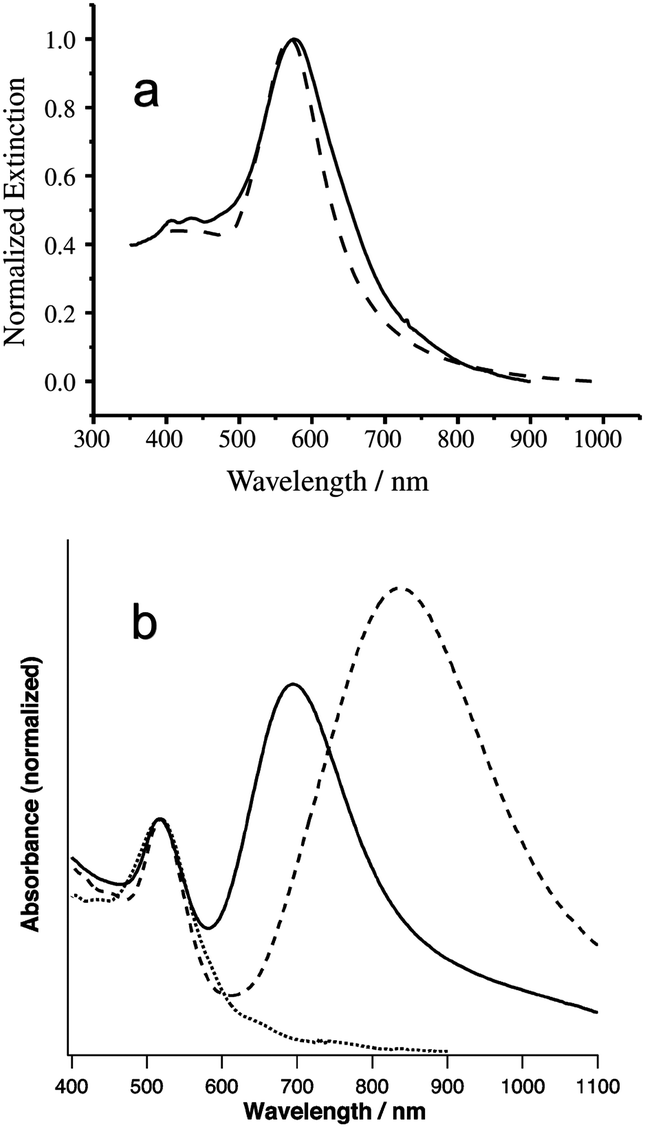 | ||
| Fig. 1 Extinction spectra of colloidal water solutions of gold nanospheres and nanorods. (a) Nanospheres (diameter 100 nm), observed (solid curve) and calculated with Mie scattering theory (dashed curve).22 (b) Nanospheres (diameter 15–25 nm, dotted curve), nanorods of low aspect ratio (solid curve), nanorods of high aspect ratio (dashed curve). Extinction is normalised at ∼520 nm.15 Reproduced with permission from ref. 22. Copyright 2004, Elsevier. Reproduced with permission from ref. 15. Copyright 2006, The Royal Society of Chemistry. | ||
Anisotropic nanoparticles: nanorods as typical examples
The optical properties of metal nanostructures depend strongly on their geometrical structures. In gold nanorods, for example, strong resonance extinction bands are observed in the long wavelength region,23–26 in addition to the resonance band at approximately 530 nm that is also observed for spherical particles. The resonance at ∼530 nm is assigned to the transverse plasmon mode where the electrons oscillate orthogonally to the rod axis. The resonance in the longer wavelength (Fig. 1b),15 which shifts further to longer wavelengths with increasing aspect ratio of the rod, is attributed to the longitudinal mode parallel to the rod axis. In a nanorod with a small aspect ratio, a dipolar longitudinal mode (i.e., the lowest order mode), where the oscillation phase of the electrons is uniform over the whole rod, is observed in the long wavelength region. When the resonance peak for the dipolar mode shifts to the infrared region with increasing aspect ratio, a resonance due to another longitudinal mode appears in the visible region.27–33 The newly appeared resonance is attributed to a higher-order plasmon mode with nodes along the rod axis, where the electronic oscillation phase depends on the position on the rod. When such a mode is excited, the direction of the polarisation (and consequently the electric field that is induced) alternates along the axis of the rod (as illustrated in Fig. 2).19 In this article the index of the mode m is defined as [(the number of the nodes along the rod axis) + 1]. The dipolar mode corresponds to m = 1.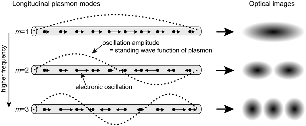 | ||
| Fig. 2 Longitudinal plasmon modes of a metal nanorod and the expected optical images observed at wavelengths resonant with the respective modes.19 Reproduced with permission from ref. 19. Copyright 2013, American Chemical Society. | ||
A mode with an even m value always possesses a node at the centre of the rod, and the direction of the collective electronic oscillation on the left half is opposite to that on the right half. Even m modes are optically forbidden if the rod size is sufficiently smaller than the wavelength of light, or if the incidence of the light is normal to the long axis of the rod. This is because the induced oscillating polarisations on both sides of the centre are in opposite directions, which results in null polarisation as a whole. The resonance frequency of the longitudinal mode becomes higher for larger m and asymptotically approaches the frequency of the transverse mode.17,26,28 The resonance wavelength is always longer than ∼530 nm. The dispersion of the transverse plasmon mode is very small compared to the longitudinal mode, and thus all the transverse modes, from the lowest dipolar mode to the high m modes, are usually observed at approximately 530 nm in the extinction spectrum of nanorods in water.
Assembled nanoparticles: sphere dimers as typical examples
Relative to isolated particles, different characteristics become apparent when two or more particles interact to form an assembly. The plasmon resonance frequency of the metal nanoparticle splits when particles assemble, because of the interaction between the plasmons excited on the particles.6,7 The extent of splitting depends on the interparticle distance, with closer distances resulting in larger splittings.The most prominent optical property of metal nanoparticle assemblies is the formation of strongly enhanced optical fields in the gaps between the particles.5–7 The enhancement occurs in the frequency region near the lower frequency side of the split plasmon resonances. For noble metal nanoparticles such as gold and silver, the electric field amplitude at the gap between the nanoparticles sometimes reaches up to a few thousand times the field in free space.34–36 It is believed that surface enhanced Raman scattering (SERS) arises from Raman active molecules in gaps such as these. On the basis of electromagnetic field simulations, numerous studies have been published on the optical field structures in noble metal nanoparticle assemblies.11,34–37 A typical example is shown in Fig. 3.36 When a spherical nanoparticle dimer is irradiated by light, a strongly enhanced optical field is generated in the gap if the incident polarisation is parallel to the interparticle axis of the dimer. The strong field in the gap is not present if the incident polarisation is perpendicular to the interparticle axis of the dimer.
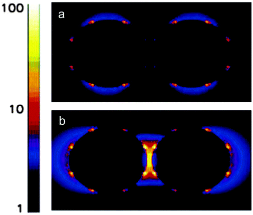 | ||
| Fig. 3 Calculated electromagnetic field for a dimer of gold nanospheres (diameter 60 nm) at a wavelength of 633 nm. The incident polarisation direction is perpendicular (a) and parallel (b) to the interparticle axis of the dimer, respectively.36 Reproduced with permission from ref. 36. Copyright 2005, American Chemical Society. | ||
Two-photon induced photoluminescence of gold nanoparticles
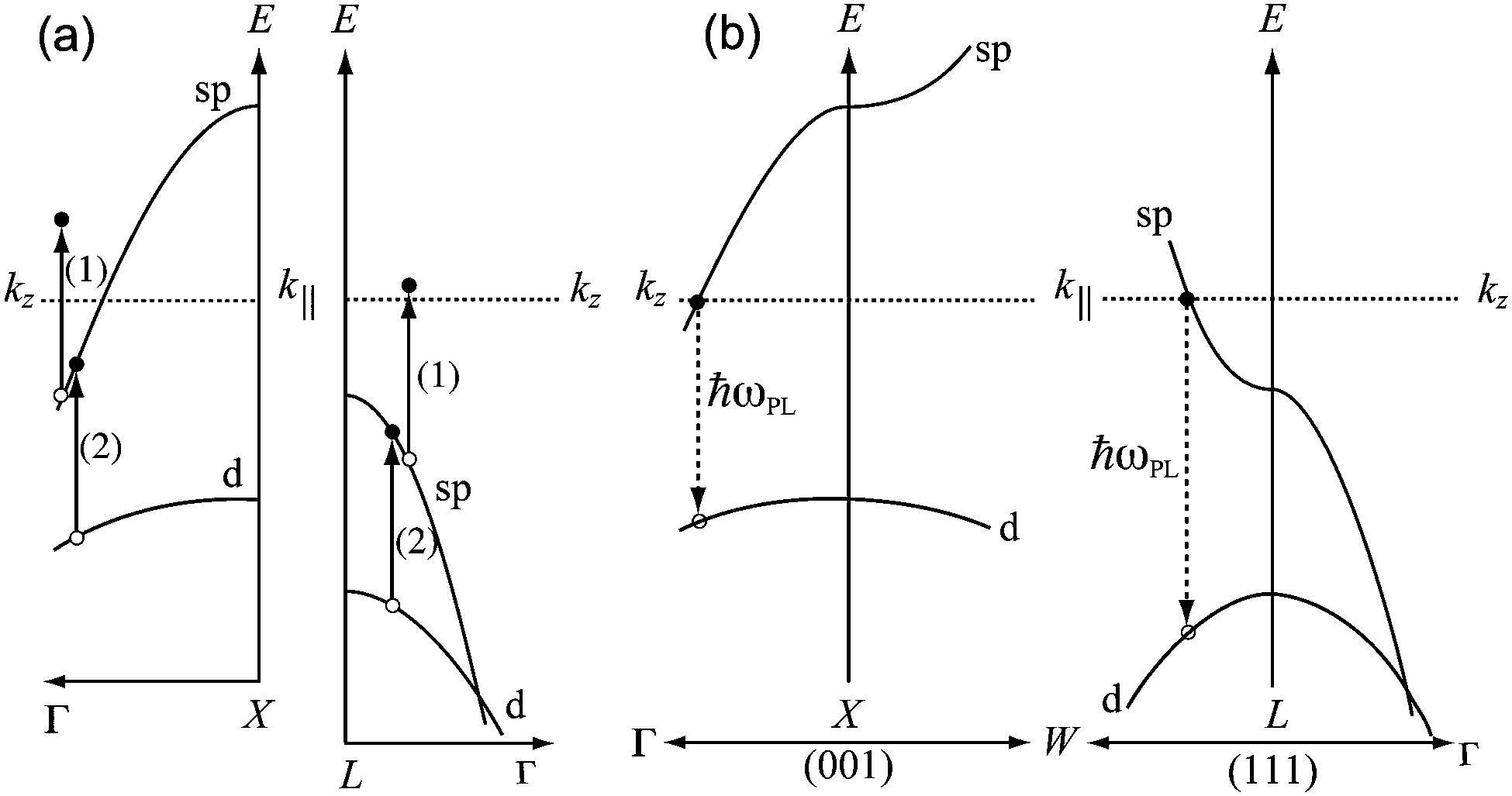
Gold has interband transitions in the visible frequency region and shows luminescence arising from electron–hole recombination.38–40 This luminescence is usually very weak in the bulk metal. However, the luminescence is relatively strong in nanoparticles, most likely because of enhancement by localised plasmon resonances.When the plasmon of a gold nanostructure is resonant with the radiation from a Ti:sapphire laser (typically at ∼800 nm), strong photoluminescence is induced via two-photon excitation with the femtosecond pulses from the Ti:sapphire laser.41–45 The mechanism of TPIPL is considered to operate as follows. A sequential two-photon excitation process (whose scheme is shown in Fig. 4(a)), with the femtosecond pulses resonant with the localised plasmon, excites the gold nanostructure. This process yields an electron in an sp band and a hole in a d band. The eventual recombination of them (Fig. 4(b)) gives two photoluminescence bands centred at ∼650 and ∼550 nm.43,46 The TPIPL from gold nanostructures is conveniently utilised for imaging experiments.
 | ||
| Fig. 4 Excitation (a) and emission (b) schemes in the band structure of gold proposed for the two-photon induced photoluminescence.43 Dashed lines indicate the Fermi surfaces. Open and closed circles in (a) denote holes and electrons, respectively. Reproduced with permission from ref. 43. Copyright 2005, American Chemical Society. | ||
2. Scanning near-field optical microscope
As mentioned above, oscillating electric fields (optical fields) with characteristic spatial features are generated on metal nanostructures when localised plasmons are excited. However, the spatial scale of the spatial feature is essentially smaller than that of the resonant optical wavelength. Consequently, the structure cannot be imaged directly by conventional optical microscopy because the highest spatial resolution is determined by the diffraction limit of light, which is on the order of the wavelength. Near-field optical microscopy is an optical method that enables a spatial resolution higher than the diffraction limit.5,6,13,14 To achieve this, an optical field confined to a nanospace in the vicinity of a nanostructured material is used. The near-field microscopic method in current practical use is classified broadly into two types: aperture type and scattering type. Herein, we do not provide a comparison between these two types of methods. In some specific cases, three-dimensional field distributions are also observable by near-field microscopy.47For the studies of plasmonic materials described in the following, the authors have adopted aperture-type near-field microscopy. The aperture-type SNOM we constructed22,48 is shown schematically in Fig. 5. An apertured optical fibre probe6,13,14,49,50 is installed to generate an optical near-field by introducing light from the other end of the fibre. The sample is irradiated by the near-field radiation from the aperture, and the scattering or the luminescence from the sample is collected and detected. The sample is scanned laterally using a nano-positioner while detecting the intensity of light from the sample to obtain an optical image of the sample. The major polarisation component near the centre of the probe aperture is in the plane of the aperture. We can select an arbitrary in-plane linear polarisation of the near-field by installing suitable polarisation optics before the light is coupled to the fibre.
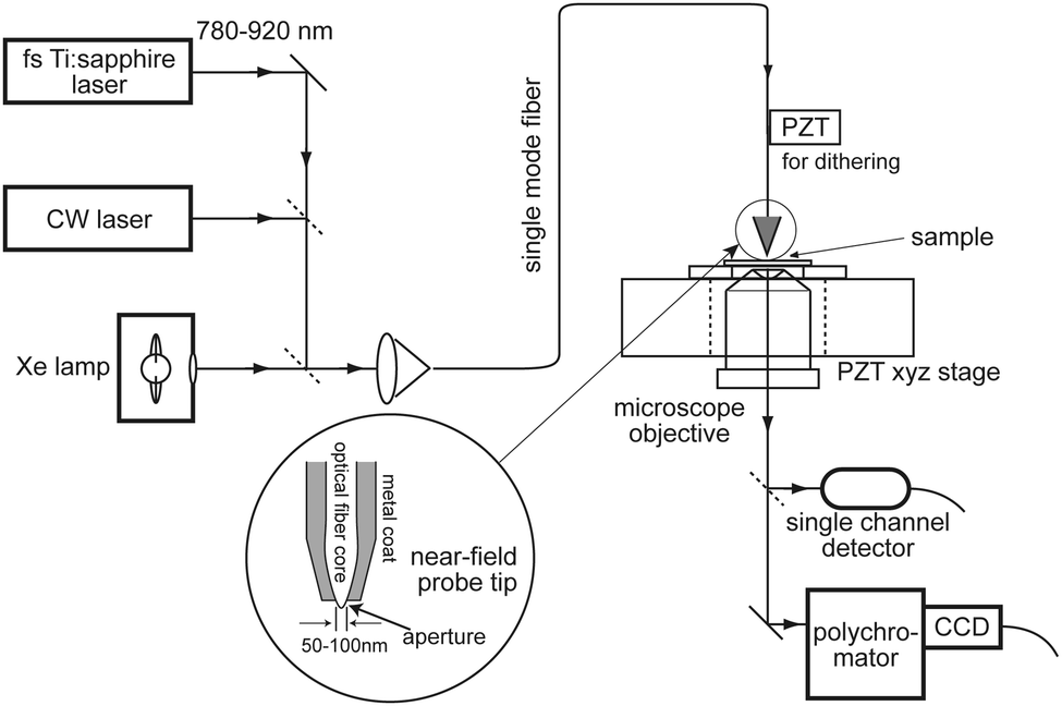 | ||
| Fig. 5 Schematic diagram of a near-field optical microscope the authors constructed. PZT: piezoelectric transducer; CCD: charge-coupled device multichannel photodetector. | ||
To obtain the signal to construct near-field optical images, we mainly adopt either one of two methods for optical detection: transmission type measurement or two-photon excitation measurement. For the transmission measurement, a discharge arc lamp or a laser is used as the light source. The transmitted light at the same wavelength as the incident light is detected.15–18,22 For the two-photon excitation measurement, an ultrashort pulsed light source, such as a femtosecond Ti:sapphire laser, is used to excite the sample.15–18,43 The pulse duration at the probe tip was typically ∼100 fs when the dispersion arising from the optical fibre was appropriately compensated. By detecting the intensity of the TPIPL from the sample, we can obtain the signal of two-photon excitation probability at the incident wavelength. The ultrashort pulsed light source is also used for the near-field imaging of ultrafast dynamics, as described later. In this case, pulses as short as ∼15 fs at the probe tip were used.
3. Plasmon-mode standing waves of single metal nanoparticles
As described previously, the longitudinal plasmons of noble metal nanorods show large dispersion, and hence the frequency of the mode depends strongly on its mode index m. In addition, the spatial distribution of the polarisation induced by the irradiation of light on the nanostructure depends on the mode index, and the spatial features of the mode can be visualised by near-field measurements with the radiation of the resonant frequency.One-dimensional systems: nanorods and elongated rectangular voids
The resonant frequency of the longitudinal plasmon of a nanorod increases (i.e., the wavelength gets shorter) as the mode index m becomes larger. When the near-field optical image of a gold nanorod is recorded, the spatial structure of the standing wave function of the plasmon mode resonant with the incident light is visualised.30,42,43,46,51–56Fig. 6 shows typical near-field transmission images of a gold nanorod to demonstrate the standing wave structure.15,18,53 In this measurement, the transmitted polarisation component parallel to the rod axis was detected, which enabled visualisation of the longitudinal modes. The observed images show spatially oscillating features along the rod axis, and the wavenumber of the spatial oscillation decreases when the wavelength of observation becomes longer. Similar features are found in standing wave functions for oscillations of one-dimensional strings. This means that the longitudinal plasmon of a nanorod can be described as a pseudo one-dimensional system, and its spatial features were visualised in the near-field image. As described earlier, the plasmon modes of even m values are optically forbidden under the conventional view of macroscopic far-field excitation. However, such modes were clearly observed in the near-field images, indicating that modes with even values of m were optically excited under the near-field irradiation. Because the material is locally excited with a confined light source under the near-field irradiation conditions, the conventional selection rule of optical transition becomes invalid. This is the reason why the even-m modes were observed in the near-field images.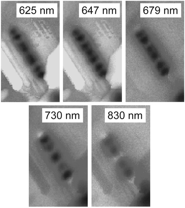 | ||
| Fig. 6 Near-field transmission images of a gold nanorod (diameter 20 nm, length 510 nm) at various wavelengths. The polarisation of the observation was parallel to the long axis of the rod.18 Reproduced with permission from ref. 18. Copyright 2013, The Chemical Society of Japan. | ||
We also observed standing waves of plasmon modes for metal nanostructures that correspond to inverted structures of nanorods on thin metallic films (i.e., elongated rectangular openings, or voids).57 As with nanorods, standing waves, as determined by the length, width, and thickness of the void, appear near the openings. The observed undulating features of the near-field images are interpreted as the visualised standing waves near the openings.
A similar observation of standing wave modes is also possible by scattering-type near-field optical microscopy.58,59 In the scattering type method, the electric field component normal to the sample plane is mainly observed. The phase-sensitive detection of the electric field is relatively easy in a scattering type experiment, and images with electric field phases relative to the incident field were reported. A typical example is shown in Fig. 7.59 Because the electric field component normal to the sample plane is detected in this measurement, the image gave intensity extrema at nodal positions of the longitudinal plasmons (Fig. 2). The electric field direction alternated along the rod (wire) axis for every node, and correspondingly the phase detected with the near-field imaging also alternated.
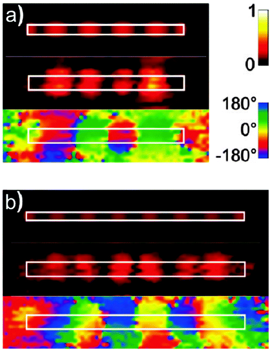 | ||
| Fig. 7 Near-field optical images of gold nanowires (width 40 nm, thickness 25 nm) taken using a scattering type near-field optical microscope. Simulated magnitude (top), measured magnitude (middle), and phase (bottom) of the optical field perpendicular to the sample plane for the (a) 890 and (b) 1270 nm long wires, respectively.59 Reproduced with permission from ref. 59. Copyright 2009, American Chemical Society. | ||
High spatial resolution imaging of metal nanostructures using advanced electron microscopic techniques, such as electron-energy-loss-spectroscopy (EELS) detected transmission electron microscopy60–62 and cathodoluminescence detected scanning electron microscopy63,64 has been reported from a number of research groups. It has been shown that these electron microscopy based techniques also achieve visualisation of plasmon modes. (An example of this will be given for a circular disk in the following subsection.) In electron microscopy, the focused electron beam yields a localised current that generates an electromagnetic field with a broad spectral range, and this localised electromagnetic field excites plasmons on metal nanostructures. Consequently, the selection rules for plasmon modes are considered to be similar to those of near-field optical measurements, while they are different from far-field measurements with propagating light.
Two-dimensional systems: nanodisks
Two-dimensional metal nanostructures possess plasmonic standing wave modes of two-dimensional geometrical structures. The spatial structures of the standing waves can be visualised by near-field imaging as one-dimensional rods are visualised. The standing wave structures of one-dimensional rods correspond to those of oscillation modes of strings, and a qualitative interpretation of the near-field images was quite straightforward. In contrast, the standing wave structures of two-dimensional systems are comparable to those of membrane oscillations, which are much more complicated than one-dimensional systems. In the past, near-field65 and far-field66 two-photon excitation images were reported for triangular and hexagonal nanocrystalline gold platelets, where images obtained were analysed numerically with electromagnetic simulations. It is difficult to interpret the observed images in an intuitive manner, and theoretical simulation is indispensable for their detailed analysis.As a typical example of two-dimensional systems, we describe here near-field imaging and analysis of gold nanodisks.67Fig. 8 shows near-field transmission images of gold nanodisks with a thickness of 35 nm and diameters of 400 and 800 nm. In the image of the 400 nm disk at an observation wavelength of 780 nm, a characteristic feature is found: two extinction extrema aligned along the direction perpendicular to the polarisation of the detected light are observed. We cannot determine solely from the image whether the polarisations at these two lobes are parallel or anti-parallel to one another. Thus, comparison of the image with theoretical simulation is indispensable to assign the feature to an oscillation mode of the disk. In this regard, we analysed the observed images based on a recently developed theoretical framework,68–72 which is an extension of Mie scattering theory. The images simulated with this theory semi-quantitatively reproduced the observed images. From the analysis we clarified that the polarisations at the two lobes observed for the 400 nm disk are parallel to one another.
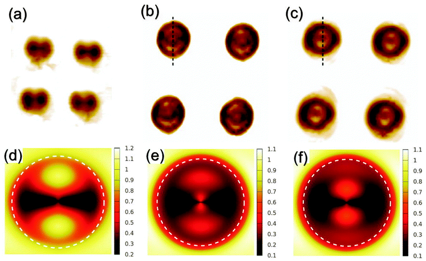 | ||
| Fig. 8 Observed (a–c) and simulated (d–f) near-field transmission images of gold nanodisks (thickness 35 nm). The diameters of the disks were 400 nm (a, d) and 800 nm (b, c, e, f). The wavelengths of observation and calculation were 780 nm (a, d), 710 nm (b), 790 nm (c), 705 nm (e) and 765 nm (f). Vertical polarisation was used for observation.67 Reproduced with permission from ref. 67. Copyright 2014, The Optical Society. | ||
Imaging the plasmons on metal nanodisks by an electron microscope based technique was also reported.73Fig. 9 shows a typical example for EELS-detected electron microscope images of a metal nanodisk. A ring-shaped feature was observed, which corresponds to an orientation average of the near-field image with the two lobes described above. The orientation average was observed in the EELS image because the polarisation direction was not defined with the electron beam. This result shows that the electron microscope based imaging gave information on plasmon modes that was consistent with that obtained by near-field imaging.
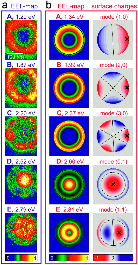 | ||
| Fig. 9 Electron energy loss (EEL) detected transmission electron micrographs of a silver nanodisk (diameter 200 nm, thickness 30 nm). (a) Experimental EEL maps. (b) Simulated EEL maps (left) and simulated surface charge distributions (right) generated by assuming the electron beam positions marked by ×.73 Reproduced with permission from ref. 73. Copyright 2012, American Chemical Society. | ||
Efficient conversion from optical near-field to propagating light by plasmon excitation
Propagating light can excite localised plasmons on metal nanostructures, and the plasmons generate localised optical near-fields in the vicinities of the nanostructures. This suggests that a metal nanoparticle has the potential to convert optical near-fields to propagating radiations, as would be expected from reciprocity. A unique phenomenon of metal nanoparticles that arises from this property was observed for gold nanodisks.74Fig. 10 shows near-field transmission spectra of gold nanodisks using a near-field probe with an aperture diameter of ∼100 nm. The spectrum was measured at the centres of the disks. In this figure, the horizontal line of unity transmittance corresponds to the intensity of light passing through the aperture probe on the bare glass substrate. Because the probe aperture diameter was ∼100 nm and the distance from the disk surface to the aperture was 20–30 nm, the disk with a diameter of 150 nm or larger completely covers the aperture. However, the transmittance substantially exceeds unity in the longer wavelength region than the plasmon resonance of the disk. This demonstrates that the transmission intensity from the probe aperture becomes stronger when the disk blocks the aperture, which is counterintuitive. Similar effects were also found for gold nanospheres22 and gold-coated dielectric sphere resonators.75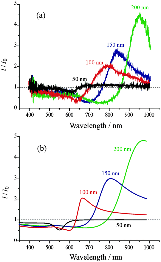 | ||
| Fig. 10 Near-field transmission spectra of single gold nanodisks (diameters 50, 100, 150 and 200 nm, height 35 nm). (a) Experiment. (b) Model simulation assuming conversion of localised near-field to propagating light by the disk.74 Reproduced with permission from ref. 74. Copyright 2011, American Chemical Society. | ||
This anomalous transmission phenomenon was successfully reproduced semi-quantitatively by a simple theoretical model calculation that incorporated scattering of optical near-field at the aperture to the propagating radiation. The result indicates that the noble metal nanoparticles, as typified by nanodisks, mutually convert optical near-fields and propagating fields very efficiently. This property of nanodisks is potentially important when plasmon resonances are utilised to enhance the efficiencies of photo-energy or photochemical conversion processes.
4. Optical field distributions in metal nanoparticle assemblies
When two or more metal nanoparticles are assembled with a suitable interparticle distance, coupled plasmon modes of the assembly are excited and strongly enhanced optical fields localised in the gaps between the particles are generated when the sample is irradiated by light because of interparticle interactions.11,34–37,76,77 In some cases, the enhancement of the optical field intensity (i.e., squared amplitude) is considered to be as high as 106–107. The major origin of SERS is believed to be the molecules that lie in the gap sites of the assemblies, where strong enhancement of the scattering field is expected.11,34–37,76–81 Visualisation of the enhanced optical fields serves as a basis for clarifying the mechanism of the enhancement and is also beneficial for application purposes. However, the spatial scales of the enhanced fields are much smaller than the optical wavelength, which prevents visualisation of the field structures by conventional optical microscopy. To address this issue we sought to visualise the localised optical fields by the use of near-field optical microscopy.Enhanced optical fields in spherical nanoparticle assemblies
As a typical example, a near-field two-photon excitation image of dimeric gold nanospheres (diameter 100 nm) is shown in Fig. 11.82–84 High photon densities were observed at the interstitial sites between the particles when the incident polarisation was nearly parallel to the interparticle axes of the dimers. In contrast, only a small enhancement of the field was observed for isolated particles and dimers whose orientations were perpendicular to the incident polarisation. The observed result is consistent with the spatial structure of the enhanced fields predicted by electromagnetic theory.11,34–37,76,77 Thus, the image can be interpreted as a visualisation of enhanced optical fields. It was also shown by comparing near-field two-photon excitation images and near-field Raman excitation images of the same dimers that the enhanced optical fields make major contributions to SERS. Recently, the enhanced optical fields for dimeric nanostructures of gold were also observed using a scattering near-field microscope with a spatial resolution higher than 10 nm (Fig. 12).85 The observed image shows a highly confined optical field along the interparticle axis.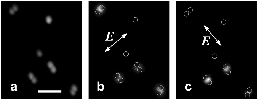 | ||
| Fig. 11 Near-field two-photon excitation images of gold nanosphere dimers (sphere diameter 100 nm). (a) Topography. (b) and (c) Two-photon excitation images. The excitation wavelength was 780 nm. Polarisation of the excited field is indicated by an arrow in each panel. The approximate positions of the nanospheres are indicated by the white circles. The scale bar is 500 nm.84 Reproduced with permission from ref. 84. Copyright 2008, The Japan Society of Applied Physics. | ||
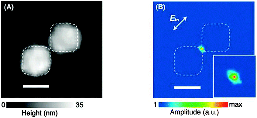 | ||
| Fig. 12 (A) Topography and (B) corresponding scattering-type near-field optical image of the nanogap antenna composed of two gold nanosquares. The inset in (B) shows the 2× magnified view around the interparticle gap area. The scale bar is 100 nm.85 Reproduced with permission from ref. 85. Copyright 2011, The Optical Society. | ||
Spatial structures of enhanced optical fields were also visualised for one-dimensional arrays86 and two-dimensional monolayered assemblies87–89 of spherical gold nanoparticles. Model analysis of the results indicated that the characteristic features of their field structures arised from the interparticle plasmonic interactions (or, in other words, the propagation of the localised plasmons in the assemblies).90
Assemblies of circular voids on thin metallic films
Ripples of localised plasmons are induced on the metal thin film around the aperture when an aperture opened on a thin metallic film is irradiated by light.91–93 This plasmon excitation generates a localised optical field in the vicinity of the aperture, which is similar to what occurs in a metal nanoparticle. Like the nanoparticle assemblies that yield enhanced local optical fields, arrays of apertures on a thin metallic film have the potential to confine optical fields. Fig. 13 shows near-field two-photon excitation images of linear arrays of circular apertures on gold thin films.94 We find localised optical fields at positions between the circular apertures in these images when the incident polarisation is parallel to the array. These features may also be utilised for the purpose of localising the optical fields.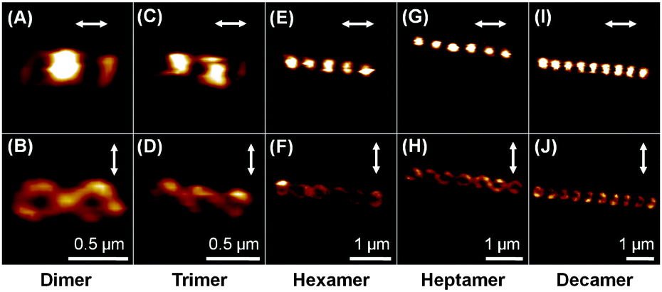 | ||
| Fig. 13 Near-field two-photon excitation images of a dimer (A, B), a trimer (C, D), a hexamer (E, F), a heptamer (G, H) and a decamer (I, J) of nanovoids (diameter ∼400 nm) on a gold film (thickness ∼20 nm). The excitation polarisation direction is indicated in each panel by an arrow. The excitation wavelength was 785 nm.94 Reproduced with permission from ref. 94. Copyright 2011, American Chemical Society. | ||
5. Dynamics of plasmon excitations
The characteristics of plasmons are closely related to their dynamic properties, and many time-resolved studies have been devoted to revealing the dynamics of plasmonic materials. The dynamics of plasmons are of fundamental importance in applications of plasmonic materials.23,95–107 For instance, when plasmonic materials are used as components of optical communication devices, knowledge about the plasmon dynamics is indispensable to attain higher throughput. From this viewpoint, ultrafast measurements of metal waveguide structures and coherent control of plasmonic field with pulse shaping technique were conducted. A typical example is shown in Fig. 14.108 In this work, deterministic control of the plasmonic field was attempted for a metal wave guide structure having one port of light incidence and three output ports. The incident waveforms were controlled to yield Fourier transform limited plasmon pulses at the targeted output ports.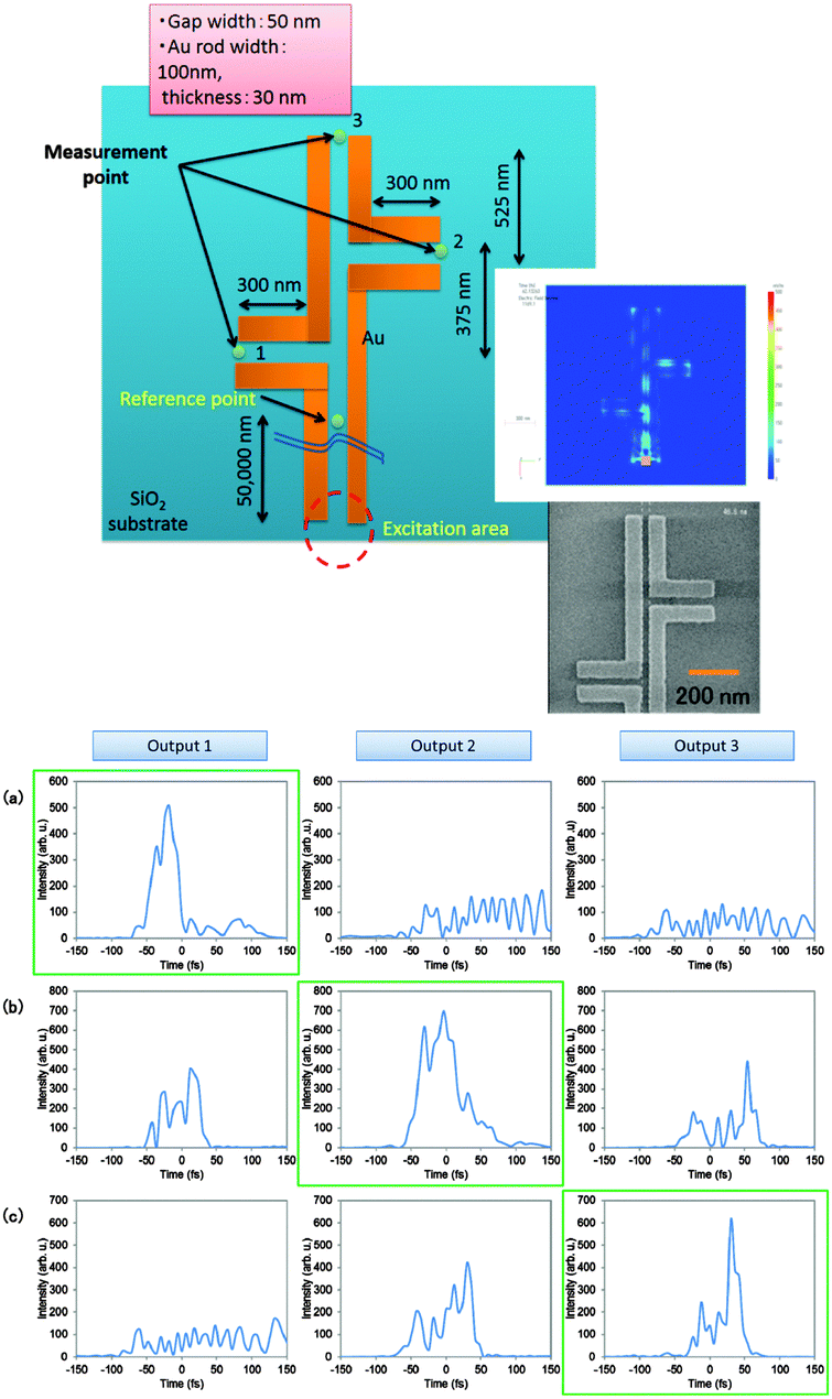 | ||
| Fig. 14 (top) An air-gap surface plasmon-polariton waveguide designed for the demonstration of plasmon propagation control by pulse shaping. The inset shows a theoretical prediction for plasmon propagation in this waveguide. The scanning electron micrograph is also shown. (bottom) Time histories of plasmon pulses measured at the three exits of the waveguide. The excitation laser pulse was shaped so that the Fourier transform limited plasmon appears at (a) Exit 1, (b) Exit 2 and (c) Exit 3.108 Reproduced with permission from ref. 108. Copyright 2013, The Optical Society. | ||
In the application of plasmons to photo-energy or photochemical conversions, knowledge about the plasmon dynamics is again necessary to enhance the efficiency of the target process relative to various other competing processes. From this perspective, we performed ultrafast near-field optical measurements of gold nanoparticles to directly analyse the correlation between dynamics and the spatial characteristics of the plasmons.
Relaxation processes following plasmon excitations
The localised plasmon on a noble metal nanoparticle is excited immediately following photoirradiation, and the initial (ground) state is recovered after various relaxation processes of different timescales.109 Plasmon resonance is the collective oscillation of conduction electrons, and it is thus damped by the dephasing (and photoemission) process. The rate of dephasing depends on the dielectric nature of the constituent metal and the shape and size of the nanostructure. The typical dephasing time of a gold nanoparticle plasmon in the visible to near-infrared frequency region is a few fs to ∼20 fs.110 After the dephasing of the plasmon, the particle undergoes transition to electronically excited states involving specific electrons,98 and then to a thermal pseudo-equilibrium state as a result of electron–electron scattering.23,96,97,111 The excess energy is gradually distributed to lattice vibrations and other degrees of freedom on the sub-picosecond timescale to yield a thermal equilibrium for the particle.23,95,97,98,112,113 Finally, the system, including the bath, recovers the initial equilibrium state in pico- to nanoseconds. Because the unique properties of the plasmons arise from the resonance state prior to dephasing, time-resolved measurements with a resolution higher than 20 fs are necessary to obtain information on the essential dynamics of the plasmons.Method of ultrafast near-field measurements
For ultrafast measurements, particularly with a time resolution higher than ∼10 fs, the equal pulse correlation method,114,115 in which one ultrashort pulse is divided into two pulses of nearly equivalent characteristics, is widely adopted. The divided pulses are incident on the sample as the pump and probe pulses after the optical delay line between the two pulses. In our near-field ultrafast measurements,48,51,116,117 the pump and probe beams were generated using a Michelson interferometer and collinearly coupled to the optical fibre to irradiate the sample from the probe aperture. Regarding the signal to construct the images, we detected either transient transmission changes of the optical intensities after they passed through the sample or TPIPL from the gold sample. By recording the signal as a function of delay time between the pump and probe pulses, the time-resolved signal at a position of the probe tip was obtained. Finally, we obtained time-resolved near-field optical images by performing this measurement at each position on the sample.Because the optical pulses pass through quite long dispersive media (such as optical fibre) in the near-field microscopes, the pulse duration at the probe aperture is exceedingly broadened when very short optical pulses are used. To compensate for the dispersion effects arising from the optical components, passive dispersion compensation devices (such as a grating pair)118 were used, which were adjusted to yield the optimum pulse width at the probe aperture.48,51,116 In the time-resolved experiments with a time resolution of nearly 10 fs, a pulse shaping technique using a spatial phase modulator is sometimes introduced,119,120 in addition to the passive dispersion compensation devices. In our group, we achieved a pulse duration of ∼15 fs at the probe aperture with this method.
Dynamics in gold nanorods following photoexcitation
As mentioned previously, thermal processes following plasmon dephasing are observed by time-resolved measurements with a time resolution on the order of 100 fs. The near-field time-resolved transient transmission signal change at each point on a nanorod was composed of a sub-picosecond component attributed to electron–electron scattering and a picosecond component arising from electron–phonon scattering.51 Near-field transient transmission images in the sub-picosecond regime after plasmon excitation showed a characteristic spatially oscillating feature along the rod axis.121 Based on a model analysis, we found that the feature is caused by distortion of the plasmonic standing wave function that follows the electronic temperature rise after photoexcitation.Time-resolved measurements with a time-resolution on the order of 10 fs have the potential to allow observation of the dynamics before the dissipation of plasmons. Thus, we performed ultrafast near-field measurements using the TPIPL detection for gold nanorods.122,123 We found a plasmon dephasing time that was nearly independent of the position on the rod when the light pulse excites only one resonant plasmon mode on the rod. In contrast, when the spectrum of the light pulse covered two or more plasmon resonances, the observed dynamics were dependent on the position (Fig. 15). This phenomenon occurred because of the broad nature of the ultrashort pulse, which made a multi-mode coherent excitation possible. The transient near-field image showed features that varied with the delay time between the pump and probe pulses. This result can be explained as a result of the plasmon wave packet propagation after coherent excitation of multiple modes.
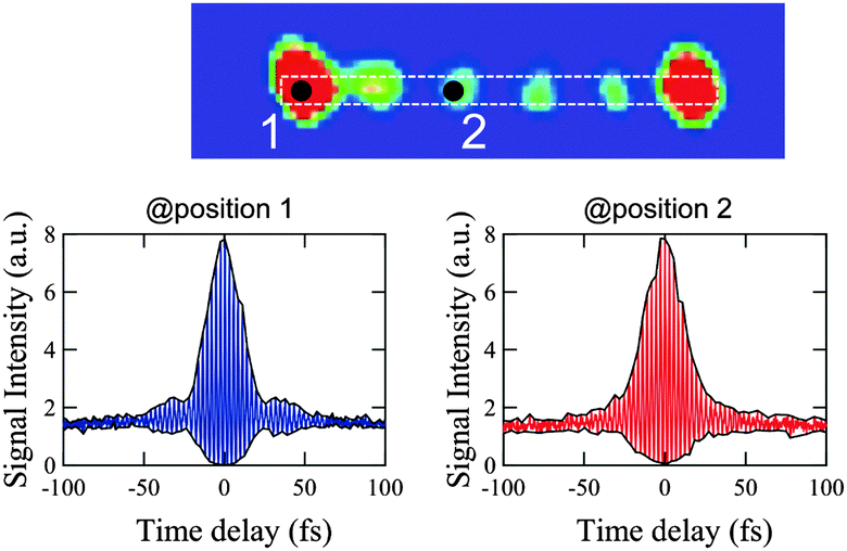 | ||
| Fig. 15 (top) Near-field two-photon excitation image of a single gold nanorod (length 1000 nm, width 70 nm, height 20 nm) observed at 870 nm. (bottom) Time-resolved near-field two-photon excitation traces observed at positions 1 and 2 marked in the image. The dynamic behaviours are found to be different between the two positions. | ||
6. Observation of chiral plasmons
Chirality and optical activity in two-dimensional systems
A molecule shows optical activity when it has a chiral geometric structure (i.e., if the molecule is not identical to its mirror image).124,125 In a similar way, a two-dimensional nanostructure fixed on a plane shows optical activity when it possesses two-dimensional chirality (i.e., the geometry does not superimpose on its mirror image in the plane). It was recently demonstrated for chiral noble metal nanostructures that optical activities stronger than those for molecules were observed at wavelengths resonant with their plasmons.126–130 It has also been reported that the detection sensitivity of the optical activity signals from some chiral molecules is enhanced enormously when the molecule is placed near a chiral metal nanostructure.131,132 Theoretical studies noted that achiral metal nanoparticles potentially enhance the optical activity signals from molecules.133 It is expected that optical fields with enhanced optical chirality134 are generated in the vicinity of noble metal nanostructures at the wavelengths of plasmon resonances,135–138 which are considered to be the major origin of the strong optical activities.To investigate the mechanisms of these phenomena and to design and exploit such chiral optical fields, analyses of the spatial distributions of local optical activity on the nanostructures and the resonant plasmon modes must be highly informative. From this point of view, we have developed an apparatus for near-field circular dichroism measurements that achieves imaging of local optical activity with a spatial resolution on the order of nanometres, and have analysed the local optical activity of a few prototypical two-dimensional gold nanostructures.
Method of near-field measurements of local optical activity
Sub-micrometre imaging of local optical activity based on a far-field nonlinear optical method was reported for noble metal nanostructures.139–142 For example, the chirality of plasmonic excitations on gold nanostructures was studied based on a far-field second-harmonic imaging method with circularly polarised light (Fig. 16).142 In this case, variation of the chiral optical field distribution with a change of nanostructures and/or their structural parameters was visualised and analysed. A few reports have been previously published on near-field measurements of circular dichroism (CD),143,144 but the technique was not applied to local optical activities of metal nanostructures. Recently, we developed an apparatus with higher detection sensitivity of CD signals while maintaining a 100 nm (or higher) spatial resolution.145–148 This design enabled a closer approach to the CD of metal nanostructures than has previously been made possible.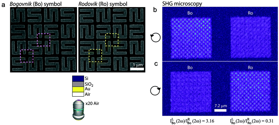 | ||
| Fig. 16 Far-field second harmonic generation (SHG) CD images of chiral metal nanostructures. (a) Scanning electron micrograph of the Bogovnik (Bo) and Rodovik (Ro) traditional Slavic symbols. (b, c) SHG microscopy of the Bo and Ro sample arrays upon illumination with left- and right-circularly polarised light, respectively.142 Reproduced with permission from ref. 142. Copyright 2014, Wiley-VCH. | ||
Our CD imaging method is based on the combination of aperture type near-field optical microscopy and the circular polarisation modulation method adopted in most conventional CD spectrometers.149 A beam from a monochromatic linearly polarised light source (laser) is passed through a photoelastic modulator (PEM), which modulates the light periodically between left- and right-handed circular polarisations at a repetition rate of several tens of kilohertz. This light was incident on the gold nanostructure sample through a microscope objective. The transmitted radiation was detected with the near-field aperture probe near the sample nanostructure following its interaction with the sample, and its intensity was recorded. Lock-in detection of the signal synchronised with the polarisation modulation by the PEM provided the summation and difference of the transmission intensities for the left- and right-handed circular polarisations. We obtained the CD signal (i.e., the absorbance difference between the left- and right-handed circular polarisations) at the probe position. We can construct a near-field CD image by collecting the local CD signals at every lateral point of the sample. Because of the inherent characteristic of PEMs, there is a possibility that linear dichroism (LD) signals commingle with the CD signals. When necessary, a rotating half-wave plate was inserted before the polarisation-modulated light becomes incident on the sample to suppress the commingling of the LD signals.
CD imaging of chiral and achiral gold nanostructures
We studied a two-dimensional “S”-shaped gold nanostructure and its mirror imaged structure fabricated on a glass substrate with the electron-beam lithography lift-off method.145–147 Prominent CD signals on the order of 10−3 in absorbance units were observed in the macroscopic CD spectra of these samples measured with a propagating light, and the signs of the signals for “S” and mirrored “S” were mutually inverted.146Fig. 17 shows near-field CD images of S-shaped and its mirrored counterpart gold nanostructures of the same sizes, and the profiles of the CD signals along the curves of the structures. Positive and negative signals coexisted in the single S-shaped structures (i.e., the signal oscillated along the curves), and the extremal values of the signals were on the order of 10−1, which is roughly two-orders of magnitude stronger than the signal strength recorded for the macroscopic measurements. The line profiles of the CD signals were approximately symmetric with respect to the centres of the structures, and the profiles for “S” and mirrored “S” were anti-phase to one another. This indicates that the distribution of the local CD signals correctly reflected the symmetry of the nanostructure.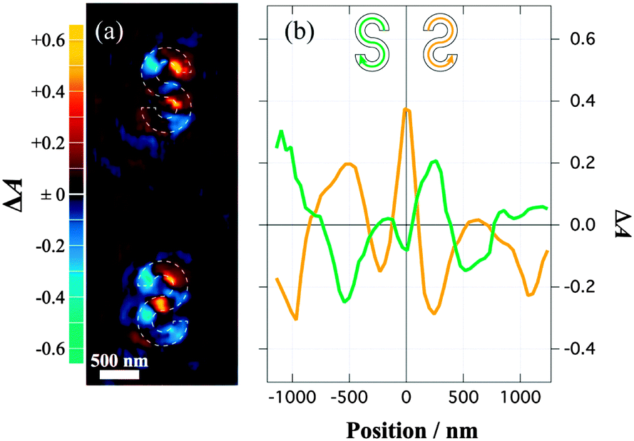 | ||
| Fig. 17 (a) Near-field CD images of S-shaped and mirrored S-shaped gold nanostructures measured at 785 nm. (b) Line profiles along the curves of the S-shaped structures.146 Reproduced with permission from ref. 146. Copyright 2013, American Chemical Society. | ||
The local CD signals observed in the images were found to be much stronger than the macroscopic signals, which may be caused by cancellation of the major part of positive and negative signals coexisting in the nanostructure. Conversely, it may be suggested that nanostructures giving only small macroscopic CD signals (or even null signals, as mentioned below) potentially yield strong local CD signals. This situation may be relevant to the theoretical prediction of large optical chirality in the vicinities of metal nanostructures.136–138 Such locally large chirality of optical fields in metal nanostructures may provide valuable insight for designing nanostructures to detect molecular chirality.131–133
To investigate the factor(s) that causes the local optical activity of chiral metal nanostructures, we decomposed the “S”-shaped structure into two “C”-shaped partial structures and measured the variation of the CD signals as the two “C”-shaped structures approached one another.147 We fabricated a series of nanostructures with varying distance between the two “C” structures to form a mirrored “S” structure, as shown in Fig. 18. The CD signal at the central part of the system (i.e., the connecting region of the two “C” structures) was found to increase as the two “C”-shaped structures became closer, and the signal increase began before the two “C” structures were in physical contact. This result indicates that the development of the optical activity with approaching partial structures originated from long-range electromagnetic interactions and not from electronic exchange between the partial structures. A detailed theoretical investigation is necessary in future studies to clarify the mechanism of this interaction.
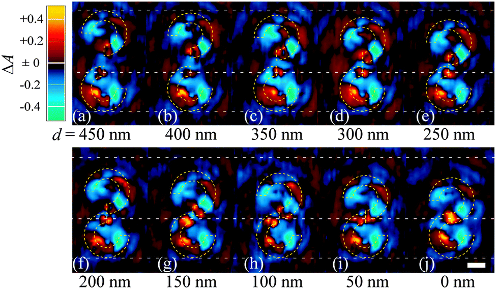 | ||
| Fig. 18 Near-field CD images of two C-shaped nanostructures approaching to form a mirrored S-shaped structure observed at 785 nm. The distance between the C-shaped nanostructures (d) was varied from 450 to 0 nm. The scale bar is 300 nm.147 Reproduced with permission from ref. 147. Copyright 2014, American Chemical Society. | ||
Both positive and negative CD signals were observed locally in single “S”-shaped gold nanostructures, as mentioned before. The “S”-shaped structure is chiral in the two-dimensional plane and gives a macroscopic CD signal. However, we also found experimentally that even a highly symmetric achiral two-dimensional nanostructure gives positive and negative local CD signals.148Fig. 19 shows a near-field CD image of a gold rectangle (310 nmL × 170 nmW × 50 nmT) observed at 633 nm. The macroscopic CD signal of this gold nanostructure was null within the experimental uncertainty, which is consistent with the conventional selection rule of CD. However, positive and negative CD signals coexisted in the inner part of the rectangle in the near-field CD image in a similar fashion to the “S”-shaped structure case. The CD signal extrema were on the order of 10−1. Both the positive and negative signals were symmetrically distributed with respect to the centre of the rectangle, which correctly reflected the symmetry of the system, and the amplitudes of the positive and negative signals were approximately equal. Consequently, the integrated signal value over the entire structure was nearly null, which is consistent with the macroscopic CD signal. Note that the local chirality and local optical activity discussed here are for a single nanostructured material with a fixed geometry and is essentially different from what is found for racemic mixtures.
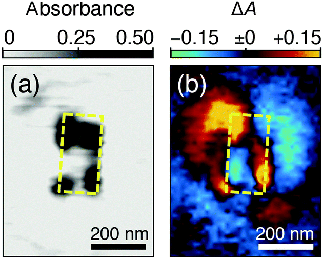 | ||
| Fig. 19 Near-field optical images of a single gold nanorectangle. (a) Near-field extinction and (b) near-field CD images observed at 633 nm. The dashed lines indicate the position of the rectangle.148 Reproduced with permission from ref. 148. Copyright 2014, American Chemical Society. | ||
These results indicate that the conventional selection rule of optical activity of molecules and materials, or the correspondence between the chirality and the optical activity, is not valid for local optical activity of nanostructures. This is interpreted to arise from the local geometrical chirality. To illustrate, when one stands at the upper left or lower right corner and faces the inner direction of a rectangle, the long and short sides become the right- and left-hand sides, respectively, whereas at the lower left or upper right corner, they become the left- and right-hand sides, respectively. The upper left (or lower right) and the lower left (or upper right) corners are mutually mirror-imaged and cannot be superposed to one another, which means that the corners are locally chiral.
The possibility of local optical chirality for achiral nanostructures was previously discussed based on theoretical simulations.137,138 In the present study, the local optical activity of achiral nanostructures has been experimentally demonstrated by measuring the CD signals with a 100 nm level spatial resolution beyond the diffraction limit. The result reminds us to be careful when applying the conventional selection rule of optical activity used throughout the field of spectroscopy. At the same time, it suggests a possible novel method of chiral molecular detection. It has now become manifest that both chiral and achiral gold nanostructures show locally strong CD signals. However, the plasmon modes that yield the optical activity and the mechanism for this process are not yet sufficiently clear and require additional study.
7. Concluding remarks
We have described that scanning near-field optical microscopy is sometimes very useful to visualise the spatial structures of optical fields arising from plasmon resonances, and that some plasmon fields are understandable only by visualising their structures. Visualisation of nanoscale optical fields will continue to be a valuable tool for studying the optical characteristics of metal nanostructures and their application. The combination of near-field microscopy and various modern spectroscopic techniques may also provide additional information and extend the research field. Ultrafast measurements and optical activity in the near-field regime described above are examples of such combinations. The design of nanoscale optical field structures and enhancement based on plasmon resonances of metal nanostructures has the potential to introduce revolutions in photochemistry, photophysics, and relevant application studies. Additionally, it may have an impact on various research fields and their applications, including high-sensitivity chemical analysis, novel photochemical reactions, photofabrication processes, photoenergy conversion, material conversion, and so forth. The rational design of these materials is also anticipated to influence photophysics and its applications, and the study of bioimaging. As a basis to promote such applications, visualisation of optical fields induced by plasmon resonances may serve as a fundamental and essential methodology.As for the development of theoretical methods to analyse the experimentally obtained results, the present situation is not sufficient in view of treating realistic moderately complex systems. One of the facts that make the theoretical treatment of near-field data difficult is that the system for measurement is in close proximity to the sample system and can electromagnetically interact with the sample. Progress of theoretical frameworks, including useful model construction for near-field measurements, is highly desired to enable the accurate analysis of experimental data with practical computing resources.
Acknowledgements
We are grateful to the collaborators who contributed to this research project, in particular, Dr T. Nagahara, Dr H. J. Wu, Mr S. Hashiyada, Ms A. Ishikawa, Prof. J. K. Lim, Ms Y. C. Kim, Mr S. Kim, Prof. D. H. Jeong, Prof. K. Ueno, Prof. H. Misawa, Dr M. K. Hossain, Dr T. Shimada, Prof. M. Kitajima, Dr S. I. Kim, Prof. S. Kim, Mr D. McArthur, Dr B. Hourahine, and Dr F. Papoff. The authors are also indebted to the Equipment Development Center and the Laser Research Center for Molecular Science of Institute for Molecular Science. This research was supported by Grants from the Ministry of Education, Culture, Sports, Science and Technology (No. 17034062, 19049015 and 25109713), the Japan Society for the Promotion of Science (No. 16350015, 17655011, 18205004, 18685003, 21655008, 22225002, 24655020, and 24350014), the Japan Science and Technology Agency PRESTO, and the Kurata Science Foundation. The project was also supported in part by the Extreme Photonics Project, the Consortium for Photon Science and Technology, the Nanotechnology Platform Program, and the Cooperative Research Program of Network Joint Research Center for Materials and Devices.Notes and references
- M. Kerker, The Scattering of Light and Other Electromagnetic Radiation, Academic Press, New York, 1969 Search PubMed.
- R. H. Ritchie, Surf. Sci., 1973, 34, 1–19 CrossRef CAS.
- C. F. Bohren and D. R. Huffman, Absorption and Scattering of Light by Small Particles, Wiley, New York, 1983 Search PubMed.
- U. Kreibig and M. Vollmer, Optical Properties of Metal Clusters, Springer, Berlin, Heidelberg, 1995 Search PubMed.
- Near-field Optics and Surface Plasmon Polaritons, Topics in Applied Physics, ed. S. Kawata, Springer, Berlin, Heidelberg, vol. 81, 2001 Search PubMed.
- L. Novotny and B. Hecht, Principle of Nano-optics, Cambridge University Press, Cambridge, 2006 Search PubMed.
- S. A. Maier, Plasmonics: Fundamentals and Applications, Springer, New York, 2007 Search PubMed.
- J. I. Gersten, J. Chem. Phys., 1980, 72, 5779–5780 CrossRef CAS PubMed.
- P. F. Liao and A. Wokaun, J. Chem. Phys., 1982, 76, 751–752 CrossRef CAS PubMed.
- M. B. Mohamed, V. Volkov, S. Link and M. A. El-Sayed, Chem. Phys. Lett., 2000, 317, 517–523 CrossRef CAS.
- M. Futamata, Y. Maruyama and M. Ishikawa, J. Phys. Chem. B, 2003, 107, 7607–7617 CrossRef CAS.
- K. L. Kelly, E. Coronado, L. L. Zhao and G. C. Schatz, J. Phys. Chem. B, 2003, 107, 668–677 CrossRef CAS.
- Near-Field Nano/Atom Optics and Technology, ed. M. Ohtsu, Springer, Tokyo, 1998 Search PubMed.
- D. Courjon, Near-Field Microscopy and Near-Field Optics, Imperial College Press, London, 2003 Search PubMed.
- H. Okamoto and K. Imura, J. Mater. Chem., 2006, 16, 3920–3928 RSC.
- K. Imura and H. Okamoto, Bull. Chem. Soc. Jpn., 2008, 81, 659–675 CrossRef CAS.
- H. Okamoto and K. Imura, Prog. Surf. Sci., 2009, 84, 199–229 CrossRef CAS PubMed.
- H. Okamoto and K. Imura, Bull. Chem. Soc. Jpn., 2013, 86, 397–413 CrossRef CAS.
- H. Okamoto and K. Imura, J. Phys. Chem. Lett., 2013, 4, 2230–2241 CrossRef CAS.
- G. Mie, Ann. Phys., 1908, 25, 377–445 CrossRef CAS.
- M. Born and E. Wolf, Principles of Optics, Cambridge University Press, Cambridge, 7th expanded edn, 1999 Search PubMed.
- K. Imura, T. Nagahara and H. Okamoto, Chem. Phys. Lett., 2004, 400, 500–505 CrossRef CAS PubMed.
- S. Link and M. A. El-Sayed, J. Phys. Chem. B, 1999, 103, 8410–8426 CrossRef CAS.
- S. Link, M. B. Mohamed and M. A. El-Sayed, J. Phys. Chem. B, 1999, 103, 3073–3077 CrossRef CAS; S. Link and M. A. El-Sayed, J. Phys. Chem. B, 2005, 109, 10531–10532 CrossRef.
- H. Kuwata, H. Tamaru, K. Esumi and K. Miyano, Appl. Phys. Lett., 2003, 83, 4625–4627 CrossRef CAS PubMed.
- E. K. Payne, K. L. Shuford, S. Park, G. C. Schatz and C. A. Mirkin, J. Phys. Chem. B, 2006, 110, 2150–2154 CrossRef CAS PubMed.
- J. R. Krenn, G. Schider, W. Rechberger, B. Lamprecht, A. Leitner, F. R. Aussenegg and J. C. Weeber, Appl. Phys. Lett., 2000, 77, 3379–3381 CrossRef CAS PubMed.
- G. Schider, J. R. Krenn, A. Hohenau, H. Ditlbacher, A. Leitner, F. R. Aussenegg, W. L. Schaich, I. Puscasu, B. Monacelli and G. Boreman, Phys. Rev. B: Condens. Matter Mater. Phys., 2003, 68, 155427 CrossRef.
- W. L. Schaich, G. Schider, J. R. Krenn, A. Leitner, F. R. Aussenegg, I. Puscasu, B. Monacelli and G. Boreman, Appl. Opt., 2003, 42, 5714–5721 CrossRef CAS.
- A. Hohenau, J. R. Krenn, G. Schider, H. Ditlbacher, A. Leitner, F. R. Aussenegg and W. L. Schaich, Europhys. Lett., 2005, 69, 538–543 CrossRef CAS.
- K. Ueno, V. Mizeikis, S. Juodkazis, K. Sasaki and H. Misawa, Opt. Lett., 2005, 30, 2158–2160 CrossRef.
- K. Ueno, S. Juodkazis, V. Mizeikis, K. Sasaki and H. Misawa, J. Am. Chem. Soc., 2006, 128, 14226–14227 CrossRef CAS PubMed.
- K. Ueno, S. Juodkazis, M. Mino, V. Mizeikis and H. Misawa, J. Phys. Chem. C, 2007, 111, 4180–4184 CAS.
- H. Xu, J. Aizpurua, M. Käll and P. Apell, Phys. Rev. E: Stat. Phys., Plasmas, Fluids, Relat. Interdiscip. Top., 2000, 62, 4318–4324 CrossRef CAS.
- E. Hao and G. C. Schatz, J. Chem. Phys., 2004, 120, 357–366 CrossRef CAS PubMed.
- C. E. Talley, J. B. Jackson, C. Oubre, N. K. Grady, C. W. Hollars, S. M. Lane, T. R. Huser, P. Nordlander and N. J. Halas, Nano Lett., 2005, 5, 1569–1574 CrossRef CAS PubMed.
- K. Li, M. I. Stockman and D. J. Bergman, Phys. Rev. Lett., 2003, 91, 227402 CrossRef.
- A. Mooradian, Phys. Rev. Lett., 1969, 22, 185–187 CrossRef CAS.
- G. T. Boyd, Z. H. Yu and Y. R. Shen, Phys. Rev. B: Condens. Matter Mater. Phys., 1986, 33, 7923–7936 CrossRef CAS.
- E. Dulkeith, T. Niedereichholz, T. A. Klar, J. Feldmann, G. von Plessen, D. I. Gittins, K. S. Mayya and F. Caruso, Phys. Rev. B: Condens. Matter Mater. Phys., 2004, 70, 205424 CrossRef.
- A. Bouhelier, M. R. Beversluis and L. Novotny, Appl. Phys. Lett., 2003, 83, 5041–5043 CrossRef CAS PubMed.
- K. Imura, T. Nagahara and H. Okamoto, J. Am. Chem. Soc., 2004, 126, 12730–12731 CrossRef CAS PubMed.
- K. Imura, T. Nagahara and H. Okamoto, J. Phys. Chem. B, 2005, 109, 13214–13220 CrossRef CAS PubMed.
- A. Bouhelier, R. Bachelot, G. Lerondel, S. Kostcheev, P. Royer and G. P. Wiederrecht, Phys. Rev. Lett., 2005, 95, 267405 CrossRef CAS.
- R. A. Farrer, F. L. Butterfield, V. W. Chen and J. T. Fourkas, Nano Lett., 2005, 5, 1139–1142 CrossRef CAS PubMed.
- K. Imura and H. Okamoto, J. Phys. Chem. C, 2009, 113, 11756–11759 CAS.
- S. Ezugwu, H. Yea and G. Fanchini, Nanoscale, 2015, 7, 252–260 RSC.
- T. Nagahara, K. Imura and H. Okamoto, Rev. Sci. Instrum., 2004, 75, 4528–4533 CrossRef CAS PubMed.
- E. Betzig, J. K. Trautman, T. D. Harris, J. S. Weiner and R. L. Kostelak, Science, 1991, 251, 1468–1470 CAS.
- N. Hosaka and T. Saiki, Opt. Rev., 2006, 13, 262–265 CrossRef CAS.
- K. Imura, T. Nagahara and H. Okamoto, J. Phys. Chem. B, 2004, 108, 16344–16347 CrossRef CAS.
- K. Imura, T. Nagahara and H. Okamoto, J. Chem. Phys., 2005, 122, 154701 CrossRef PubMed.
- K. Imura and H. Okamoto, Opt. Lett., 2006, 31, 1474–1476 CrossRef.
- J. K. Lim, K. Imura, T. Nagahara, S. K. Kim and H. Okamoto, Chem. Phys. Lett., 2005, 412, 41–45 CrossRef CAS PubMed.
- K. Imura, Y. C. Kim, S. Kim, D. H. Jeong and H. Okamoto, Phys. Chem. Chem. Phys., 2009, 11, 5876–5881 RSC.
- D. Denkova, N. Verellen, A. V. Silhanek, V. K. Valev, P. V. Dorpe and V. V. Moshchalkov, ACS Nano, 2013, 7, 3168–3176 CrossRef CAS PubMed.
- K. Imura, K. Ueno, H. Misawa and H. Okamoto, J. Phys. Chem. C, 2013, 117, 2449–2454 CAS.
- M. Schnell, A. García-Etxarri, A. J. Huber, K. Crozier, J. Aizpurua and R. Hillenbrand, Nat. Photonics, 2009, 3, 287–291 CrossRef CAS.
- J. Dorfmüller, R. Vogelgesang, R. T. Weitz, C. Rockstuhl, C. Etrich, T. Pertsch, F. Lederer and K. Kern, Nano Lett., 2009, 9, 2372–2377 CrossRef PubMed.
- D. Rossouw, M. Couillard, J. Vickery, E. Kumacheva and G. A. Botton, Nano Lett., 2011, 11, 1499–1504 CrossRef CAS PubMed.
- B. S. Guiton, V. Iberi, S. Li, D. N. Leonard, C. M. Parish, P. G. Kotula, M. Varela, G. C. Schatz, S. J. Pennycook and J. P. Camden, Nano Lett., 2011, 11, 3482–3488 CrossRef CAS PubMed.
- I. Alber, W. Sigle, S. Müller, R. Neumann, O. Picht, M. Rauber, P. A. van Aken and M. E. Toimil-Molares, ACS Nano, 2011, 5, 9845–9853 CrossRef CAS PubMed.
- E. J. R. Vesseur, R. de Waele, M. Kuttge and A. Polman, Nano Lett., 2007, 7, 2843–2846 CrossRef CAS PubMed.
- M. W. Knight, L. Liu, Y. Wang, L. Brown, S. Mukherjee, N. S. King, H. O. Everitt, P. Nordlander and N. J. Halas, Nano Lett., 2012, 12, 6000–6004 CrossRef CAS PubMed.
- K. Imura, T. Nagahara and H. Okamoto, Appl. Phys. Lett., 2006, 88, 023104 CrossRef PubMed.
- J. Fedou, S. Viarbitskaya, R. Marty, J. Sharma, V. Paillard, E. Dujardin and A. Arbouet, Phys. Chem. Chem. Phys., 2013, 15, 4205–4213 RSC.
- K. Imura, K. Ueno, H. Misawa, H. Okamoto, D. McArthur, B. Hourahine and F. Papoff, Opt. Express, 2014, 22, 12189–12199 CrossRef CAS PubMed.
- F. Papoff and B. Hourahine, Opt. Express, 2011, 19, 21432–21444 CrossRef CAS PubMed.
- K. Holms, B. Hourahine and F. Papoff, J. Opt. A: Pure Appl. Opt., 2009, 11, 054009 CrossRef.
- B. Hourahine, K. Holms and F. Papoff, J. Phys.: Conf. Ser., 2012, 367, 012010 CrossRef.
- B. Hourahine and F. Papoff, Meas. Sci. Technol., 2012, 23, 084002 CrossRef.
- D. McArthur, B. Hourahine and F. Papoff, Phys. Sci. Int. J., 2014, 4, 565–575 CrossRef.
- F. P. Schmidt, H. Ditlbacher, U. Hohenester, A. Hohenau, F. Hofer and J. R. Krenn, Nano Lett., 2012, 12, 5780–5783 CrossRef CAS PubMed.
- K. Imura, K. Ueno, H. Misawa and H. Okamoto, Nano Lett., 2011, 11, 960–965 CrossRef CAS PubMed.
- D. Amarie, T.-D. Onuta, R. A. Potyrailo and B. Dragnea, J. Phys. Chem. B, 2005, 109, 15515–15519 CrossRef CAS PubMed.
- J. Jiang, K. Bosnick, M. Maillard and L. Brus, J. Phys. Chem. B, 2003, 107, 9964–9972 CrossRef CAS.
- J. R. Lakowicz, Anal. Biochem., 2005, 337, 171–194 CrossRef CAS PubMed.
- M. Moskovits, Rev. Mod. Phys., 1985, 57, 783–826 CrossRef CAS.
- K. Kneipp, Y. Wang, H. Kneipp, L. T. Perelman, I. Itzkan, R. R. Dasari and M. S. Feld, Phys. Rev. Lett., 1997, 78, 1667–1670 CrossRef CAS.
- S. Nie and S. R. Emory, Science, 1997, 275, 1102–1106 CrossRef CAS PubMed.
- A. M. Michaels, M. Nirmal and L. E. Brus, J. Am. Chem. Soc., 1999, 121, 9932 CrossRef CAS.
- K. Imura, H. Okamoto, M. K. Hossain and M. Kitajima, Chem. Lett., 2006, 35, 78–79 CrossRef CAS.
- K. Imura, H. Okamoto, M. K. Hossain and M. Kitajima, Nano Lett., 2006, 6, 2173–2176 CrossRef CAS PubMed.
- H. Okamoto and K. Imura, Jpn. J. Appl. Phys., 2008, 47, 6055–6062 CrossRef CAS.
- Y. Tanaka, H. Ishiguro, H. Fujiwara, Y. Yokota, K. Ueno, H. Misawa and K. Sasaki, Opt. Express, 2011, 19, 7726–7733 CrossRef CAS PubMed.
- T. Shimada, K. Imura, H. Okamoto and M. Kitajima, Phys. Chem. Chem. Phys., 2013, 15, 4265–4269 RSC.
- M. K. Hossain, T. Shimada, M. Kitajima, K. Imura and H. Okamoto, J. Microsc., 2008, 229, 327–330 CrossRef CAS PubMed.
- T. Shimada, K. Imura, M. Hossain, H. Okamoto and M. Kitajima, J. Phys. Chem. C, 2008, 112, 4033–4035 CAS.
- M. K. Hossain, T. Shimada, M. Kitajima, K. Imura and H. Okamoto, Langmuir, 2008, 24, 9241–9244 CrossRef CAS PubMed.
- H. Okamoto, K. Imura, T. Shimada and M. Kitajima, J. Photochem. Photobiol., A, 2011, 221, 154–159 CrossRef CAS PubMed.
- T. Rindzevicius, Y. Alaverdyan, B. Sepulveda, T. Pakizeh, M. Käll, R. Hillenbrand, J. Aizpurua and F. J. G. de Abajo, J. Phys. Chem. C, 2007, 111, 1207–1212 CAS.
- L. Yin, V. K. Vlasko-Vlasov, A. Rydh, J. Pearson, U. Welp, S. H. Chang, S. K. Gray, G. C. Schatz, D. B. Brown and C. W. Kimball, Appl. Phys. Lett., 2004, 85, 467–469 CrossRef CAS PubMed.
- S. H. Chang, S. K. Gray and G. C. Schatz, Opt. Express, 2005, 13, 3150–3165 CrossRef.
- S. I. Kim, K. Imura, S. Kim and H. Okamoto, J. Phys. Chem. C, 2011, 115, 1548–1555 CAS.
- T. S. Ahmadi, S. L. Logunov and M. A. El-Sayed, J. Phys. Chem., 1996, 100, 8053–8056 CrossRef CAS.
- N. Del Fatti, C. Voisin, M. Achermann, S. Tzortzakis, D. Christofilos and F. Vallée, Phys. Rev. B: Condens. Matter Mater. Phys., 2000, 61, 16956–16966 CrossRef CAS.
- C. Voisin, N. Del Fatti, D. Christofilos and F. Vallée, J. Phys. Chem. B, 2001, 105, 2264–2280 CrossRef CAS.
- O. P. Varnavski, M. B. Mohamed, M. A. El-Sayed and T. Goodson III, J. Phys. Chem. B, 2003, 107, 3101–3104 CrossRef CAS.
- A. Kubo, Y. S. Jung, H. K. Kim and H. Petek, J. Phys. B: At., Mol. Opt. Phys., 2007, 40, S259–S272 CrossRef CAS.
- A. Kubo, K. Onda, H. Petek, Z. Sun, Y. S. Jung and H. K. Kim, Nano Lett., 2005, 5, 1123–1127 CrossRef CAS PubMed.
- A. Kubo, N. Pontius and H. Petek, Nano Lett., 2007, 7, 470–475 CrossRef CAS PubMed.
- J. H. Hodak, A. Henglein and G. V. Hartland, J. Phys. Chem. B, 2000, 104, 9954–9965 CrossRef CAS.
- M. A. van Dijk, M. Lippitz and M. Orrit, Phys. Rev. Lett., 2005, 95, 267406 CrossRef.
- L. Bonacina, A. Callegari, C. Bonati, F. van Mourik and M. Chergui, Nano Lett., 2006, 6, 7–10 CrossRef CAS PubMed.
- L. Zhang, A. Kubo, L. Wang, H. Petek and T. Seideman, Phys. Rev. B: Condens. Matter Mater. Phys., 2011, 84, 245442 CrossRef.
- L. Wang, Y. Nishijima, K. Ueno, H. Misawa and N. Tamai, Appl. Phys. Lett., 2009, 95, 053116 CrossRef PubMed.
- L. Wang, A. Kiya, Y. Okuno, Y. Niidome and N. Tamai, J. Chem. Phys., 2011, 134, 054501 CrossRef PubMed.
- S. Onishi, K. Matsuishi, J. Oi, T. Harada, M. Kusaba, K. Hirosawa and F. Kannari, Opt. Express, 2013, 21, 26631–26641 CrossRef PubMed.
- S. Link and M. A. El-Sayed, Annu. Rev. Phys. Chem., 2003, 54, 331–366 CrossRef CAS PubMed.
- C. Sönnichsen, T. Franzl, T. Wilk, G. von Plessen, J. Feldmann, O. Wilson and P. Mulvaney, Phys. Rev. Lett., 2002, 88, 077402 CrossRef.
- C. Voisin, D. Christofilos, P. A. Loukakos, N. Del Fatti, F. Vallée, J. Lermé, M. Gaudry, E. Cottancin, M. Pellarin and M. Broyer, Phys. Rev. B: Condens. Matter Mater. Phys., 2004, 69, 195416 CrossRef.
- O. L. Muskens, N. Del Fatti and F. Vallée, Nano Lett., 2006, 6, 552–556 CrossRef CAS PubMed.
- M. Pelton, M. Liu, S. Park, N. F. Scherer and P. Guyot-Sionnest, Phys. Rev. B: Condens. Matter Mater. Phys., 2006, 73, 155419 CrossRef.
- M. J. Rosker, F. W. Wise and C. L. Tang, Phys. Rev. Lett., 1986, 57, 321–324 CrossRef CAS.
- J.-C. Diels and W. Rudolph, Ultrashort Laser Pulse Phenomena, Academic Press, Burlington, 2nd edn, 2006 Search PubMed.
- T. Nagahara, K. Imura and H. Okamoto, Chem. Phys. Lett., 2003, 381, 368–375 CrossRef CAS PubMed.
- H. J. Wu, Y. Nishiyama, T. Narushima, K. Imura and H. Okamoto, Appl. Phys. Express, 2012, 5, 062002 CrossRef.
- S. Smith, N. C. R. Holme, B. Orr, R. Kopelman and T. Norris, Ultramicroscopy, 1998, 71, 213–223 CrossRef CAS.
- K. Furusawa, N. Hayazawa, T. Okamoto, T. Tanaka and S. Kawata, Opt. Express, 2011, 19, 25328–25336 CrossRef PubMed.
- S. Berweger, J. M. Atkin, X. G. Xu, R. L. Olmon and M. B. Raschke, Nano Lett., 2011, 11, 4309–4313 CrossRef CAS PubMed.
- K. Imura and H. Okamoto, Phys. Rev. B: Condens. Matter Mater. Phys., 2008, 77, 041401(R) CrossRef.
- Y. Nishiyama, T. Narushima, K. Imura and H. Okamoto, Ultrafast Phenomena XIX, Springer, Cham, 2015, pp. 691–693 Search PubMed.
- Y. Nishiyama et al., to be submitted.
- N. Berova, K. Nakanishi and R. W. Woody, Circular Dichroism: Principles and Applications, Wiley-VCH, New York, 2nd edn, 2000 Search PubMed.
- L. D. Barron, Molecular Light Scattering and Optical Activity, Cambridge University Press, Cambridge, 2004 Search PubMed.
- A. Papakosatas, A. Potts, D. M. Bangnall, S. L. Provirnin, H. J. Coles and N. I. Zheludev, Phys. Rev. Lett., 2003, 90, 107404 CrossRef.
- T. Vallius, K. Jefimovs, J. Turunen, P. Vahimaa and Y. Svirko, Appl. Phys. Lett., 2003, 83, 234–236 CrossRef CAS PubMed.
- M. Kuwata-Gonokami, N. Saito, Y. Ino, M. Kauranen, K. Jefimovs, T. Vallius, J. Turunen and Y. Svirko, Phys. Rev. Lett., 2005, 95, 227401 CrossRef.
- A. Drezet, C. Genet, J. Y. Laluet and T. W. Ebbesen, Opt. Express, 2008, 16, 12559–12570 CrossRef.
- M. Hentschel, M. Schäferling, B. Metzger and H. Giessen, Nano Lett., 2013, 13, 600–606 CrossRef CAS PubMed.
- E. Hendry, T. Carpy, J. Johnston, M. Popland, R. V. Mikhaylovskiy, A. J. Lapthorn, S. M. Kelly, L. D. Barron, N. Gadegaard and M. Kadodwala, Nat. Nanotechnol., 2010, 5, 783–787 CrossRef CAS PubMed.
- N. A. Abdulrahman, Z. Fan, T. Tonooka, S. M. Kelly, N. Gadegaard, E. Hendry, A. O. Govorov and M. Kadodwala, Nano Lett., 2012, 12, 977–983 CrossRef CAS PubMed.
- A. García-Etxarri and J. A. Dionne, Phys. Rev. B: Condens. Matter Mater. Phys., 2013, 87, 235409 CrossRef.
- T. Tang and A. E. Cohen, Phys. Rev. Lett., 2010, 104, 163901 CrossRef.
- E. Hendry, R. V. Mikhaylovskiy, L. D. Barron, M. Kadodwala and T. J. Davis, Nano Lett., 2012, 12, 3640–3644 CrossRef CAS PubMed.
- M. Schäferling, D. Dregely, M. Hentschel and H. Giessen, Phys. Rev. X, 2012, 2, 031010 Search PubMed.
- M. Schäferling, X. Yin and H. Giessen, Opt. Express, 2012, 20, 26326 CrossRef PubMed.
- T. J. Davis and E. Hendry, Phys. Rev. B: Condens. Matter Mater. Phys., 2013, 87, 085405 CrossRef.
- V. K. Valev, Langmuir, 2012, 28, 15454–15471 CrossRef CAS PubMed.
- V. K. Valev, B. D. Clercq, X. Zheng, D. Denkova, E. J. Osley, S. Vandendriessche, A. V. Silhanek, V. Volskiy, P. A. Warburton, G. A. E. Vandenbosch, M. Ameloot, V. V. Moshchalkov and T. Verbiest, Opt. Express, 2012, 20, 256–264 CrossRef CAS PubMed.
- V. K. Valev, J. J. Baumberg, C. Sibilia and T. Verbiest, Adv. Mater., 2013, 25, 2517–2534 CrossRef CAS PubMed.
- V. K. Valev, J. J. Baumberg, B. De Clercq, N. Braz, X. Zheng, E. J. Osley, S. Vandendriessche, M. Hojeij, C. Blejean, J. Mertens, C. G. Biris, V. Volskiy, M. Ameloot, Y. Ekinci, G. A. E. Vandenbosch, P. A. Warburton, V. V. Moshchalkov, N. C. Panoiu and T. Verbiest, Adv. Mater., 2014, 26, 4074–4081 CrossRef CAS PubMed.
- M. Savoini, P. Biagioni, G. Lakhwani, S. C. J. Meskers, L. Duò and M. Finazzi, Opt. Lett., 2009, 34, 3571–3573 CrossRef CAS PubMed.
- T. Ishibashi, T. Yoshida, A. Iijima, K. Sato, Y. Mitsuoka and K. Nakajima, J. Microsc., 1999, 194, 374–377 CrossRef CAS.
- T. Narushima and H. Okamoto, Phys. Chem. Chem. Phys., 2013, 15, 13805–13809 RSC.
- T. Narushima and H. Okamoto, J. Phys. Chem. C, 2013, 117, 23964–23969 CAS.
- T. Narushima, S. Hashiyada and H. Okamoto, ACS Photonics, 2014, 1, 732–738 CrossRef CAS.
- S. Hashiyada, T. Narushima and H. Okamoto, J. Phys. Chem. C, 2014, 118, 22229–22233 CAS.
- R. Kuroda, T. Harada and Y. Shindo, Rev. Sci. Instrum., 2001, 72, 3802–3810 CrossRef CAS PubMed.
| This journal is © the Owner Societies 2015 |