
 Open Access Article
 This Open Access Article is licensed under a
 Creative Commons Attribution 3.0 Unported Licence
A facile electrochemical route to the preparation of uniform and monoatomic copper shells for gold nanoparticles
Y.
Gründer†
*a,
Q. M.
Ramasse
b and
R. A. W.
Dryfe
a
aSchool of Chemistry, University of Manchester, Oxford Road, Manchester M13 9PL, UK
bSuperSTEM Laboratory, SciTech Daresbury Campus, Daresbury WA4 4AD, UK
First published on 22nd January 2015
Abstract
Copper on gold forms a monolayer deposit via underpotential deposition. For gold particles adsorbed at a liquid–liquid interface this results in a uniform one monolayer thick shell. This approach offers a new route for the uniform functionalisation of nanoparticles and presents a way to probe fundamental processes that underlie nanoparticle synthesis.
There is significant current interest in the electrocatalytic properties of nanoparticles, and in routes to modify particles through, for example, electrodeposition. Due to their high surface to bulk ratio, nanoparticles possess high catalytic activity and core shell nano-materials in particular are a promising way of making low cost electrocatalysts.1,2 Size and shape control of particles during growth can be achieved through sub-monolayer or monolayer deposition of a second metal on the growing particle.3 Nano-materials are conventionally suspended on a conducting solid substrate, e.g. carbon materials,4 oxides,5 metals6 or molecular templates,7 allowing formation of an electronic contact, required to control electrochemical reactions, between the nanoparticle and the supporting substrate.
This has the disadvantage that the recorded electrochemical response might be influenced by the charging of the substrate itself and that only parts of the particle surface can be accessed for the reaction. Thus being able to study the growth process in solution without a solid substrate present, but under controlled conditions, would be a great advantage for further understanding and developing of nanoparticle preparation. In this paper we present a new approach to modify gold nanoparticles suspended at an immiscible liquid interface in the absence of a solid substrate. By dissolving oxidizing or reducing agents in one of the phases, electrodeposition at the particles can be driven through applying an interfacial potential. The adsorption of particles at the liquid–liquid interface has been studied theoretically8–11 and experimentally12–14 and it was shown that charge stabilized particles from a colloidal solution can be irreversibly adsorbed at a liquid–liquid interface. In addition the effect of those adsorbed particles at the liquid–liquid interface on catalytic reactions at the interface has been investigated.15,16 We have extended these studies towards the investigation of copper underpotential deposition (upd) on gold nanoparticles supported at the liquid–liquid interface. Copper upd is widely used to obtain atomic layer core–shell particles through subsequent galvanostatic replacement of the copper monolayer with catalytically more active materials such as platinum. The upd on nanoparticles is fundamentally of interest as the stability of the monolayer is believed to depend on the particle size.17–19
Electrochemical measurements at the aqueous-1,2-dichlorobenzene (DCB) interface were carried out. The aqueous solution employed was 0.09 M LiCl + 10 mM HCl + 1 mM CuCl2. The organic electrolyte employed was 15 mM bis(triphenylphosphoranylidene)-tetrakis[3,5-bis(trifluoromethyl)phenyl]borate (BTPPATPBF). The organic phase contained 4 mM 1,1-dimethylferrocene as a reducing agent (E0 = 0.57 V vs. SCE)20 to induce deposition of the copper from the aqueous solution. Homemade Ag/AgCl reference electrodes (RE) were directly immersed in the chloride containing aqueous phase. An aqueous solution of 0.1 mM LiCl and 1 mM BTPPACl (bis(triphenylphosphoranylidene)ammonium chloride) was brought in contact with the organic solution and formed a liquid junction for the organic reference electrode. The cyclic voltammetry was recorded using a four-electrode cell. Citrate stabilized gold nanoparticles were obtained from Sigma-Aldrich.
Fig. 1a shows the cyclic voltammetry for interfacial charge transfer recorded with a scan rate of 20 mV s−1 after adsorption of either 5 nm, or 20 nm, diameter gold particles. The bulk deposition/dissolution of copper onto these gold nanoparticles is observed at an applied potential of about ΔΦ = 0.55 V. Two additional voltammetric waves are visible, one at a potential of ΔΦ = 0.016 V and the other at about ΔΦ = 0.25 V. The former corresponds to the ion transfer of the oxidized electron donor 1,1′-dimethylferrocene,20 which was used to adjust the absolute potential scale of the cyclic voltammograms. The current wave at ΔΦ = 0.25 V most likely corresponds to the upd of copper onto the gold nanoparticles. For verification a cyclic voltammogram in the same cell composition has been reported employing a bipolar setup16,21 using a polycrystalline gold wire to separate the two solutions phases, and is shown in Fig. 1b. The same absolute potential scale as for the liquid–liquid cyclic voltammetry was applied. Again, the bulk copper deposition/dissolution is observed around a potential of ΔΦ = 0.55 V. The current wave at about 0.2 V corresponding to the upd of copper onto polycrystalline gold suggests that the current wave observed for the gold particles at about 0.25 V corresponds to the copper upd.22 The gold mass concentrations of the two colloidal gold solutions with different particle diameters of 5 nm and 20 nm were the same (196.97 g mol−1). Therefore the surface area of gold per volume solution would be about four times larger for the 5 nm colloidal solution compared to the 20 nm colloidal solution16 however the aliquots of the colloidal solution added were 200 μl of the 5 nm particles and 250 μl of the 20 nm nanoparticles, resulting in a 3.2 times larger surface area for the 5 nm particles compared to the 20 nm particles. This fact is assumed to account for the difference in current which is especially visible in the potential region of the upd. The copper upd and the bulk deposition of the copper occur at the same potentials for both particle sizes.
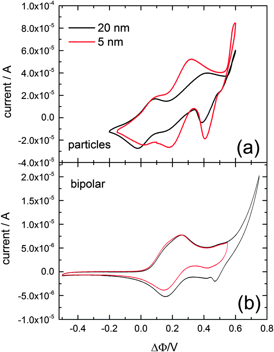 | ||
| Fig. 1 Cyclic voltammograms recorded with gold particles suspended at the aqueous–DCB interface using dimethylferrocene as a reducing agent in the organic phase and copper chloride in the aqueous phase (a). Cyclic voltammograms recorded with the same composition of organic and aqueous electrolyte solution at a bipolar setup (b). | ||
High resolution TEM data and spatially resolved Electron Energy Loss Spectra (EELS) were recorded on pre-prepared particles for which the interfacial potential was adjusted to 0.277 V, i.e. within the upd region but before the onset of bulk Cu deposition. The preparation of the particles for the TEM characterization was carried out without the four electrode setup but by adjusting the interfacial potential through the addition of a common cation.23 Tetraethylammonium (TEA) and tetramethyammonium (TMA) were added as the chloride salt to the aqueous and as TPBF salt to the organic solution, each with a final concentration of 1 M in each phase. The ion transfer and thus the interfacial potential established by the presence of the common ions are 0.277 V and 0.116 V, for TMA and TEA, respectively.24 The particles were subsequently fished out with a micropipette and deposited onto Transmission Electron Microscopy (TEM) grids. The grids employed were ultrathin carbon films supported by a lacey carbon film on a 300 mesh gold (Pelco, Ted Pella Inc.). The grids were washed in ethanol to remove any remaining electrolyte. Experiments were performed on a Nion UltraSTEM100 at the SuperSTEM Laboratory in Daresbury operating in STEM mode at 100 keV primary beam energy. The probe forming optics were adjusted to generate a 0.9 Å electron probe (full width at half-maximum) with 100 pA of beam current.
A typical spectrum acquired with the probe positioned on the very outer layer of a particle, and after applying a 4 × 4 pixel binning to improve the signal to noise ratio, is shown in Fig. 2a and reveals very clearly the presence of Cu. Fig. 2b shows an unprocessed cut-out from the survey high angle annular dark field image (HAADF) used to define the mapping region (blue box). The contrast in such images is approximately proportional to the square of the atomic number Z of the elements being observed: the particles containing Au and Cu are therefore clearly visible, with a number of atomic planes resolved, while the underlying carbon support has very weak contrast.
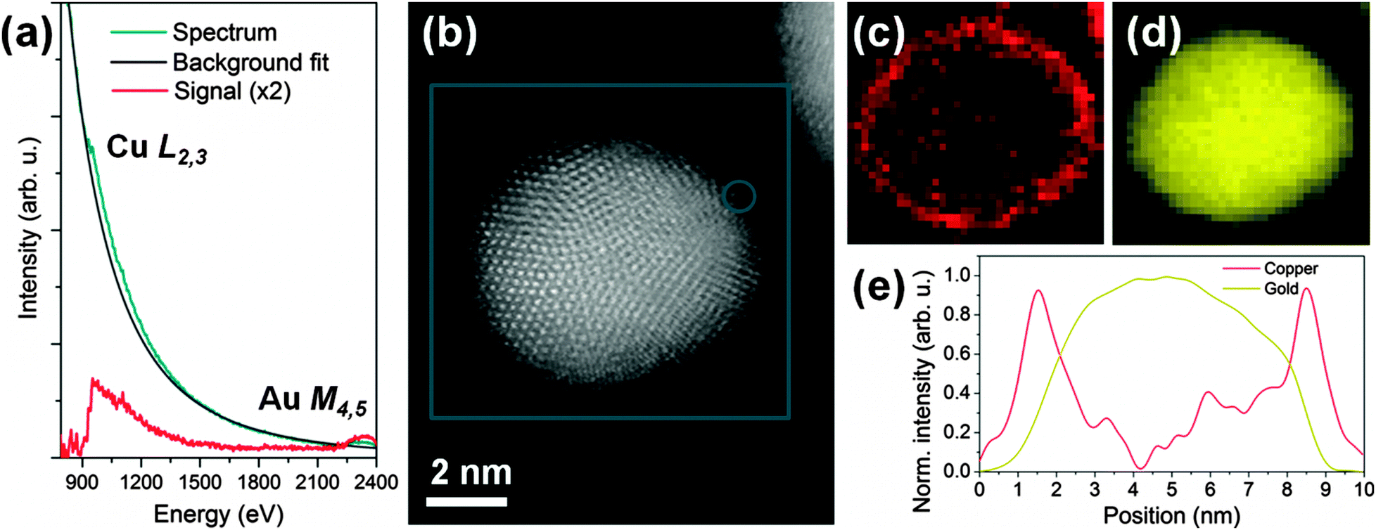 | ||
| Fig. 2 Energy electron loss spectra of a copper covered gold particle is shown (a) together with an unprocessed cut-out from the survey high angle annular dark field image (b) used to define the mapping region (blue box). The circle shows the position at which the example spectrum (a) was extracted from the map. The EELS maps are shown in (c) for Cu and (d) for Au. The linetrace in (e) corresponds to the integration over 5 pixels from top left to bottom right of the maps in (c) and (d) after normalisation to [0,1]. | ||
The corresponding chemical maps for gold and copper are shown in Fig. 2c and d, respectively, with a resolution of 1.3 Å per pixel. The EELS maps were de-noised by principal components analysis25 for copper and gold, respectively. The background was removed by fitting a power law over a region immediately in front of the core loss edges. The signal was then integrated over a 75 eV window above the onsets of the Cu L2,3 (932 eV onset) and Au M4,5 edges (2206 eV onset).
These maps reveal a continuous coverage of Cu all around the Au particle: the signal for Cu is much stronger at the edges of the particle, consistent with a well-defined, thin-core–shell geometry. A profile through these maps is shown for copper and gold in Fig. 2e. The full-width at half-maximum of the strong Cu peak at the ‘shell’ is approximately 1 nm, which is consistent with the presence of an extremely thin Cu layer. The atomic planes at the edges of the particle are clearly not perfectly parallel to the beam direction all around, so that even for a monolayer of Cu covering the Au particle, the EELS signal would be broadened due to the projection and beam propagation effects through the particle.
EELS maps with higher spatial resolution are shown in Fig. 3. The unprocessed survey image is shown in Fig. 3a: this particle was sitting on the carbon with the 〈111〉 planes well aligned with the electron beam direction, providing a clear view of the monolayer Cu cover on at least two edges. The High Angle Annular Dark field Image obtained during EELS Imaging is shown in Fig. 3b and shows that the particle rolled over during observation such that only the top edge was left on-axis. The EELS maps for copper and gold are shown in Fig. 3c and d, respectively, revealing more clearly a very thin Cu shell, whose FWHM is 6 Å, corresponding to approximately 2〈111〉 planes. Faint Cu columns are almost resolved: see white arrows on Fig. 3c. Fig. 3e shows a graphical representation of the HAADF and EELS maps from which it can be seen that the Cu signal is localised at the extreme edge of the particle, on the outmost 1–2 atomic layers, as is expected from a monolayer Cu coverage of an Au particle with an uneven outer surface.
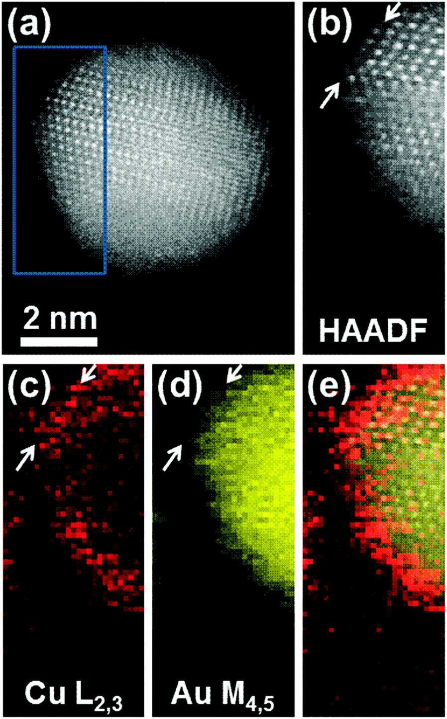 | ||
| Fig. 3 (a) Survey image: unprocessed cut-out from the survey image used to define the mapping region (b) (blue box). (c)–(e) Composite image: graphical representation using a yellow channel for Au, red for Cu and greyscale for HAADF. This shows clearly that the Cu signal is localized at the extreme edge of the particle, on the outmost atomic layers.25 | ||
Similar data acquisition was performed for particles of 5 nm diameter for which the interfacial potential was adjusted to 0.116 V, a value below the upd region, and no copper signal was detected in these cases. In the case where the copper monolayer is observed, the shell is continuously deposited over the whole particle. This suggests that the copper deposit is stable in the organic solvent constituting the liquid–liquid interface and that the particle is rotating at the interface allowing the deposition of copper from the aqueous phase over the whole particle. The recorded EELS maps including the oxygen K edge show evidence of oxygen around the particles but no evidence for a reconstructed CuO or Cu2O surface. This oxygen is likely to result from transfer through ambient atmosphere during preparation. Although the Au segregation from Cu–Au alloy nanoparticles has been observed under oxygen atmosphere26 and has also been predicted theoretically,27–29 we do not observe any decomposition with time of the copper shell. The exact stabilising mechanism for the copper shell on the nanoparticles of this size remains unclear17–19,30 but is most likely induced by electrochemical co-adsorbates. Copper upd has been reported from solution containing acetonitrile on Au(111)31 and Pt(111).32 In both cases the stabilization of the upd layer through adsorbed solvent molecules was proposed. A similar mechanism might be responsible for the stable upd layer on the DCB side of the particle.
Conclusions
In this contribution we present a new approach for the study of electrochemical processes of nanoparticles and their modification through electrodeposition without the presence of a solid substrate. We were able to form a uniform monolayer copper shell on gold particles supported at the liquid–liquid interface. This approach is thus promising for the further investigation of processes underlying nanoparticle synthesis in the solution phase.Acknowledgements
We gratefully acknowledge financial support from the EPSRC through an EPSRC-NSF “Materials World Network” grant (EP/H047786/1). The SuperSTEM Laboratory is the Engineering and Physical Sciences Research Council (EPSRC) National Facility for Aberration-corrected STEM.Notes and references
- J. Zhang, K. Sasaki, E. Sutter and R. R. Adzic, Science, 2007, 315, 220 CrossRef CAS PubMed.
- R. R. Adzic, J. Zhang, K. Sasaki, M. B. Vukmirovic, M. Shao, J. X. Wang, A. U. Nilekar, M. Mavrikakis, J. A. Valerio and F. Uribe, Top. Catal., 2007, 46, 249–262 CrossRef CAS.
- M. L. Personick, M. R. Langille, J. Zhang and C. A. Mirkin, Nano Lett., 2011, 11, 3394 CrossRef CAS PubMed.
- T. Inasaki and S. Kobayashi, Electrochim. Acta, 2009, 54, 4893–4897 CrossRef CAS PubMed.
- M. G. Mones de Oca, D. Plana, V. Celorrio, M. J. Lazaro and D. J. Fermin, J. Phys. Chem. C, 2011, 116, 692–699 Search PubMed.
- M. S. El-Deab and T. Ohsaka, Electrochim. Acta, 2002, 47, 4255–4261 CrossRef CAS.
- F. Mirkhalaf, K. Tammeveski and D. J. Schiffrin, Phys. Chem. Chem. Phys., 2009, 11, 3463–3471 RSC.
- M. C. Cecchini, V. A. Turek, J. Paget, A. A. Kornyshev and J. B. Edel, Nat. Mater., 2013, 12, 165–171 CrossRef CAS PubMed.
- A. A. Kornyshev, M. Marinescu, J. Paget and M. Urbakh, Phys. Chem. Chem. Phys., 2012, 14, 1850–1859 RSC.
- V. A. Turek, M. C. Cecchini, J. Paget, A. R. Kucernak, A. A. Kornyshev and J. B. Edel, ACS Nano, 2012, 6, 7789–7799 CrossRef CAS PubMed.
- M. Marinescu, M. Urbakh and A. A. Kornyshev, Phys. Chem. Chem. Phys., 2012, 14, 1371–1380 RSC.
- D. Schaming, M. Hojeij, N. Younan, H. Nagatani, H. J. Lee and H. H. Girault, Phys. Chem. Chem. Phys., 2011, 13, 17704–17711 RSC.
- M. Hojeij, N. Younan, L. Ribeaucourt and H. H. Girault, Nanoscale, 2010, 2, 1665–1669 RSC.
- N. Younan, M. Hojeij, L. Ribeaucourt and H. H. Girault, Electrochem. Commun., 2010, 12, 912–915 CrossRef CAS PubMed.
- J. J. Nieminen, I. Hatay, P. Y. Ge, M. A. Mendez, L. Murtomaki and H. H. Girault, Chem. Commun., 2011, 47, 5548–5550 RSC.
- Y. Gründer, M. D. Fabian, S. G. Booth, D. Plana, D. J. Fermin, P. I. Hill and R. A. W. Dryfe, Electrochim. Acta, 2013, 110, 809–815 CrossRef PubMed.
- O. A. Oviedo, C. F. A. Negre, M. M. Mariscal, C. G. Sanchez and E. P. M. Leiva, Electrochem. Commun., 2012, 16, 1–5 CrossRef CAS PubMed.
- O. A. Oviedo, M. M. Mariscal and E. P. M. Leiva, Phys. Chem. Chem. Phys., 2010, 12, 4580–4589 RSC.
- O. A. Oviedo, M. M. Mariscal and E. P. M. Leiva, Electrochim. Acta, 2010, 55, 8244–8251 CrossRef CAS PubMed.
- P. Peljo, T. Rauhala, L. Murtomaki, T. Kallio and K. Kontturi, Int. J. Hydrogen Energy, 2011, 36, 10033–10043 CrossRef CAS PubMed.
- H. Hotta, N. Akagi, T. Sugihara, S. Ichikawa and T. Osakai, Electrochem. Commun., 2002, 4, 472–477 CrossRef CAS.
- E. Herrero, L. J. Buller and H. D. Abruna, Chem. Rev., 2001, 101, 1897–1930 CrossRef CAS PubMed.
- H. H. Girault and D. J. Schiffrin, J. Electroanal. Chem., 1989, 15, 1–141 Search PubMed.
- B. Hundhammer, C. Muller, T. Solomon, H. Alemu and H. Hassan, J. Electroanal. Chem., 1991, 319, 125–135 CrossRef CAS.
- M. Watanabe, E. Okunishi and K. Ishizuka, Microsc. Anal., 2009, 23, 5–7 Search PubMed.
- E. Völker, F. J. Williams, E. J. Calvo, T. Jacob and D. J. Schiffrin, Phys. Chem. Chem. Phys., 2012, 14, 7448 RSC.
- A. U. Nilekar, A. V. Ruban and M. Mavrikakis, Surf. Sci., 2009, 603, 91 CrossRef CAS PubMed.
- A. V. Ruban and H. L. Skriver, Comput. Mater. Sci., 1999, 15, 119 CrossRef CAS.
- L.-L. Wang and D. D. Johnson, J. Am. Chem. Soc., 2009, 131, 14023 CrossRef CAS PubMed.
- O. A. Oviedo, P. Vélez, V. A. Macagno and E. P. M. Leiva, Surf. Sci., 2015, 631, 23–34 CrossRef CAS PubMed.
- K. Pekmez, E. Avci, H. Baumgärtel and C. Donner, Z. Phys. Chem., 2012, 226, 953–963 CrossRef CAS.
- A. V. Rudnev, E. B. Molodkina, A. I. Danilov, Y. M. Polukarov and J. M. Feliu, Russ. J. Electrochem., 2006, 42, 381–392 CrossRef CAS.
Footnote |
| † Current address: Department of Physics, University of Liverpool, Oxford Street, Liverpool L69 7ZE, UK. E-mail: Yvonne.grunder@liverpool.ac.uk |
| This journal is © the Owner Societies 2015 |