
 Open Access Article
 This Open Access Article is licensed under a
 Creative Commons Attribution 3.0 Unported Licence
Ordered mesoporous silica films with pores oriented perpendicular to a titanium nitride substrate
Calum
Robertson
a,
Richard
Beanland
b,
Stuart A.
Boden
c,
Andrew L.
Hector
*a,
Reza J.
Kashtiban
b,
Jeremy
Sloan
b,
David C.
Smith
d and
Alain
Walcarius
e
aChemistry, University of Southampton, Highfield, Southampton SO17 1BJ, UK. E-mail: A.L.Hector@soton.ac.uk
bDepartment of Physics, University of Warwick, Coventry CV4 7AL, UK
cElectronics and Computer Science, University of Southampton, Highfield, Southampton SO17 1BJ, UK
dPhysics and Astronomy, University of Southampton, Highfield, Southampton SO17 1BJ, UK
eLaboratoire de Chimie Physique et Microbiologie pour l'Environnement, UMR 7564, CNRS-Université de Lorraine, 405 Rue de Vandoeuvre, 54600 Villers-les-Nancy, France
First published on 7th January 2015
Abstract
The production of thin mesoporous silica films with small (∼2–3 nm) pores oriented perpendicular to a titanium nitride growth surface is demonstrated using two methods. These are the growth from a Stöber silica solution with surfactant ordering at the surface of the electrode, and electrochemically assisted growth from an acidic sol achieved by polarisation of the electrode surface. The thickness, pore order and pore size that can be achieved with these two methods is contrasted. A number of methods to vary the pore size by using different surfactants and swelling agents are explored. The advantage of applying these growth methods on titanium nitride surfaces is that it provides access to a wider electrochemical window for nanowire growth and sensor applications with non-aqueous electrolytes whilst retaining good film growth and adhesion properties.
1. Introduction
Use of porous silica structures as electrodeposition hosts to produce dense arrays of micro- or nano-structured materials has the advantage that the structures formed are electrically contacted and that the location where they grow is electrically controlled. The filling of very small (∼3 nm) pores has been demonstrated by using a supercritical fluid as the electrolyte solvent to deposit copper,1 and could provide access to nanowires in size ranges in which many materials would demonstrate large confinement energies. For instance nanowires of α-Sn should undergo a semi-metal to semiconductor transition at a diameter of ∼3 nm,2 topological insulators3 may undergo insulator to metal transitions due to the high surface area to volume ratio and nanowires with diameters down to ∼1 nm can demonstrate phase change behaviour4 hence could be used for high density memory.An ideal electrodeposition host would have pores open at one end and electrically contacted at the other end. In a thin film host that means the pores should be aligned perpendicular to the plane of the film. However, contacted wires have been grown by depositing rapidly through a 3-dimensional interconnected system, such that faster growth occurs perpendicular to the substrate, e.g. 9 nm Pt wires grown through an I![[3 with combining macron]](https://www.rsc.org/images/entities/char_0033_0304.gif) m3 silica film.5 Films with disordered pore structures can also still be used as electrodeposition hosts to produce tangled films of nanowires of metals6,7 and other materials,8 relying on diffusion through micropores in the silica walls that separate the mesopores. Electrodeposition can even be achieved in pores that are parallel to the film plane, e.g. the growth of an ordered array of parallel 3 nm wires by Suzuki et al.9 However, relying on pathways between the mesopores will lead to electrical contact between them, e.g. Suzuki's nanowire arrays were freestanding after SiO2 removal. Growth along the axis of pores that are perpendicular to the substrate surface will reduce the risk of electrical contact between wires.
m3 silica film.5 Films with disordered pore structures can also still be used as electrodeposition hosts to produce tangled films of nanowires of metals6,7 and other materials,8 relying on diffusion through micropores in the silica walls that separate the mesopores. Electrodeposition can even be achieved in pores that are parallel to the film plane, e.g. the growth of an ordered array of parallel 3 nm wires by Suzuki et al.9 However, relying on pathways between the mesopores will lead to electrical contact between them, e.g. Suzuki's nanowire arrays were freestanding after SiO2 removal. Growth along the axis of pores that are perpendicular to the substrate surface will reduce the risk of electrical contact between wires.
Silica films with ordered porosity have already found applications as electrochemical sensors,10 which are much more sensitive than their non-ordered homologues because of faster diffusion processes through the regular mesostructure.11,12 This was especially prominent with films exhibiting mesopore channels oriented normal to the underlying electrode surface.13 The sensor selectivity can also be tuned by an appropriate choice of organo-functional groups attached to the silica walls. For instance, amino-functionalized mesoporous silica films have been applied to copper(II) sensing13 while those bearing thiol groups were likely to detect mercury(II) species.14
Mesoporous silica films (pores <50 nm) are most frequently deposited by the evaporation-induced self-assembly method (EISA), in which a silica sol containing a surfactant is dip- or spin-coated onto a substrate. As the solvent evaporates the surfactant concentration increases and self-assembly into micellar structures occurs. At the same time electrostatic repulsions between the protonated silicate species in the sol are overcome and condensation accelerates.15,16 In most cases this process leads to small ordered domains in which the pores align, but these are usually either randomly oriented or have the major axis of the pores aligned parallel to the surface to maximise the interaction with the substrate.17 A number of methods have been developed to improve alignment, including the use of homopolymer–block copolymer mixtures to produce unidirectional pores parallel to a surface.18 Pores with perpendicular alignment to the surface are harder to achieve.
One method to produce readily accessible mesopores is to deposit mesoporous silica inside an anodically etched alumina membrane, where the inclination of the surfactant assemblies to lie parallel with the pore walls results in mesopores aligned with the larger pores in the alumina.19 Membranes can be back-coated with gold or attached to an electrode surface, although they inherently produce clusters of wires, one cluster per alumina pore. Such templates have been used to produce 200 nm cobalt rods consisting of a bundle of 3 nm individual wires,20 clusters of 3–5 nm gold wires attached to a carbon electrode surface,21 and 10 nm copper, silver or tellurium wires.22 However, when the deposition of 5 nm ZnO wires into such a template was attempted only very small amounts of material deposited at the end of the pores closest to the electrode.23
A number of methods have been used to produce continuous silica films with perpendicular mesopores. Films with ∼20 nm pores have been obtained by using supercritical CO2 to infiltrate tetraethyl orthosilicate (TEOS) into films of poly(α-methyl styrene-β-hydroxy styrene), which had cylindrical microdomains with the appropriate orientation.24 In an “epitaxial” approach titania with (111) oriented cubic mesopores has been used to orient the pores of a hexagonal silica film deposited onto it.25 For smaller pore sizes (∼2–3 nm), Walcarius pioneered the electrochemically assisted surfactant assembly (EASA) method, in which application of an electric field causes the self-assembly of a cetyltrimethylammonium bromide (CTAB) surfactant at the surface of an electrode.26–28 The current that then passes through the electrolyte causes the formation of hydroxide ions at the electrode surface, which locally accelerate the condensation of silicate species resulting in gelation around those assemblies and the formation of porous films up to ∼100 nm thick. Recently pore expansion in EASA films was reported using mesitylene as swelling agent, the films were poorly ordered but did exhibit an increase in the lattice parameter of the mesoporous film.29 A related route developed by Zhao produces thicker films with similar pore size from a dilute Stöber silica solution containing CTAB, which forms micelles at the substrate surface under weakly basic conditions whilst TEOS undergoes slow hydrolysis.30
The work described herein is part of the Supercritical Fluids Electrodeposition programme,31 which seeks to utilise some of the unique advantages supercritical fluids can offer in materials deposition. For deposition into small pores these advantages include the lack of surface tension, good pore penetration and improved mass transport over liquid electrolytes.32 The deposition of copper into 3 nm pores in a disordered mesoporous substrate has already been demonstrated,1 but a significant aspect of our programme is to test the limits of the technique in small pores with a range of materials. Disordered pore structures are far from ideal for this purpose, so we have focussed here on applying the Walcarius and Zhao methods described above to producing optimised mesoporous films with perpendicular pores of ∼2–4 nm. Both these methods have previously produced the highest degrees of ordering on indium tin oxide (ITO) substrates and poorer films on gold (Walcarius) or glass (Zhao). In particular film formation on noble metal surfaces suffers from poor adhesion. For template and sensor applications TiN electrodes have a number of advantages – it is extensively used as a diffusion barrier in electronic applications and has good electrochemical stability relative to ITO. This will be important in the deposition of materials that require low deposition potentials, including semiconductors such as Ge,33,34 and which cannot therefore be deposited onto ITO. Whilst in water the electrochemical window of ITO is limited by the solvent itself, in other media including organic solvents, ionic liquids and supercritical fluids, the ITO can be reduced before the solvent breakdown. Use of TiN will allow the full electrochemical stability window of these alternative solvents to be applied.
2. Experimental
200 nm titanium nitride films were deposited onto resistive Si wafers by medium frequency plasma-assisted magnetron sputtering (Leybold Optics HELIOS Pro XL) at room temperature. ITO films on glass (surface resistivity 8–12 Ω □−1), TEOS and CTAB were purchased from Sigma-Aldrich, ethanol, 37 wt% hydrochloric acid and 35 wt% ammonia solution from Fisher, and sodium nitrate from Timstar Laboratory Suppliers Ltd. The methods used to produce perpendicularly aligned mesoporous films were adapted from those previously reported by Zhao30 and Walcarius.27 An optimised procedure for each follows, although variations to these will be described later.(1) Stöber route. TEOS (0.040 cm3, 0.18 mmol) was added to a mixture of water (35 cm3), ethanol (15 cm3) and aqueous ammonia solution (35 wt% NH3, 0.0035 cm3, 0.0013 mol dm3 final sol concentration) and stirred for 2 min, then CTAB (0.080 g, 0.22 mmol) was added. The solution was stirred for a further 5 min to ensure the CTAB was fully dissolved. The 75 × 25 mm glass, ITO film on glass or TiN film on silicon substrate was submerged in the solution to a depth of ∼50 mm and sealed in a Parr 4748 Teflon-lined autoclave (125 cm3) and heated at 60 °C for 3 days. The resulting film was washed with deionized water and dried at 130 °C overnight. In order to reduce the carbon content, some films were placed into a Soxhlet extractor with a 0.1 mol dm−3 solution of HCl in EtOH and refluxed for 6 h, then rinsed with EtOH, dried, heated to 350 °C at 0.5 °C min−1 and maintained at this temperature for 5 h.
(2) EASA route. An aqueous sodium nitrate solution (0.1 mol dm−3, 20 cm3) was mixed with ethanol (20 cm3) and adjusted to pH 3 using an aqueous 0.2 mol dm−3 HCl solution. TEOS (0.905 cm3) was added and the solution allowed to stir at room temperature for 90 min. CTAB (0.47 g) was added to the solution and stirred for a further 30 min. Electrochemical cells used a silver rod pseudo-reference electrode (3.175 mm diameter, hard, Alfa Aesar) and a large area stainless steel counter electrode. Electrochemical experiments were controlled using a Biologic SP150 potentiostat. The working electrodes were 1 × 1 cm areas of ITO or TiN films. A potential of −2.0 V was applied for 5 s to the TiN electrode, or −1.3 V for 20 s for the ITO. The resulting films were washed with deionized water immediately after deposition and dried at 130 °C overnight.
Grazing incidence small angle X-ray scattering (GISAXS) experiments were conducted using a Rigaku Smartlab thin film diffractometer with a 9 kW Cu-Kα source, parallel line beam optics, in-plane arm and a DTex250 1D detector. The incident beam was a 0.1 × 5 mm line fixed at 0.25° incidence angle, and data were collected from 1–10° 2θ in in-plane and out-of-plane modes. For in-plane scans 0.5° Soller slits were used on the incident side and a 0.228° in-plane analyser on the detector side.
Scanning electron microscopy (SEM) used a Jeol JSM-6500F or a Zeiss Supra 55-VP FEGSEM microscope operating at 10–20 kV. Energy dispersive X-ray analyses (EDX) were carried out with a Thermofisher Ultradry detector with NS7 analysis platform on a Philips XL30-ESEM. Transmission electron microscopy (TEM) was conducted in a JEOL 2100 LaB6 instrument operating at 200 kV and an aberration corrected JEOL ARM200F operating at 200 kV. For cross-sectional imaging, samples were prepared by conventional mechanical polishing followed by ion beam milling, or lamellar sections were prepared in a Jeol 4500 FIB/SEM instrument. Plan view samples were prepared by scraping the mesoporous films directly onto lacey carbon grids. Helium-ion microscopy used an Orion Plus™ scanning helium ion microscope (Carl Zeiss), with an accelerating voltage of 32.2 kV, a beam current of ∼0.3 pA, a working distance of 8.6 mm, zero degrees tilt and a beam limiting aperture of 10 μm. The sample was cleaned for 8 minutes using an Evactron remote plasma cleaner (XEI Scientific, Inc) in the load lock of the microscope to reduce hydrocarbon contamination on the sample surface for high resolution imaging.35 Secondary electron images were collected using an Everhart–Thornley in-chamber secondary electron detector with a grid bias of 500 V.
Electrochemical impedance spectra were collected in 2-electrode cells vs. a Pt gauze counter electrode with a Biologic SP150 potentiostat. A 10 mV AC amplitude centred on 0 V was scanned over a frequency range 1 MHz–1 Hz. The electrolyte was 20 cm3 of a 0.05 mol dm−3 solution of nBu4NBF4 (99%, Sigma Aldrich) in acetonitrile.
3. Results and discussion
As mentioned above the literature describes two obvious methods to produce 3–4 nm mesopores perpendicular to the surface of a TiN electrode, we trial both of these.3.1 Modified Stöber route to aligned mesoporous silica films
The growth of aligned mesoporous silica on glass or ITO surfaces was originally reported by Zhao and co-workers, who suggested that a negative surface charge on the substrate leads to strong initial adsorption of the CTA+ surfactant molecules, forming spherical micellar structures.30 The negatively charged intermediates in the hydrolysis and condensation of the silane are then suggested to be attracted to the surfaces of the micelles, promoting their growth into rod-shaped structures, that the silica gel condenses around. The surface of TiN adopts a thin oxide layer36 and in the basic conditions used in Stöber silica synthesis would be expected to possess a negative charge. Hence we initially compared growth of mesoporous films on glass, ITO and TiN.Three days exposure at 60 °C of glass, ITO or TiN surfaces to a Stöber growth mixture in 30% ethanol–70% water resulted in transparent thin films with a blue, green or purple tint, of even appearance across the surface. With perpendicular pores GISAXS patterns would only be expected to show any structure in the in-plane orientation, where interference patterns due to the regular density variations in the plane of the film will result in diffraction peaks. Only very weak features were observed in out-of-plane measurements, but a strong reflection at 1.92° 2θ and a broad feature at ∼3.8° were observed in-plane. The 10 reflection of hexagonal silica with a lattice parameter of 5.31 nm is calculated to be at 1.92°, whereas the 11 and 20 reflections would be observed at 3.33 and 3.84°, respectively. We found no change in the GISAXS patterns if the CTAB concentration was increased by up to 4 times, but increasing the NH3 concentration resulted in a gradual reduction in the GISAXS intensity, most likely due to an increase in the rate of condensation reactions at higher pH.
Surfactant removal is necessary to provide open pores, and the films described herein were initially calcined in air at 450 °C to achieve this. SEM images showed smooth films without macroscopic cracks even after this treatment, and the GISAXS patterns were unchanged from those shown in Fig. 1 suggesting that the pore spacing remained constant. TEM showed hexagonal domains only typically a few pores across, which explains the broad GISAXS, and ∼2.6 nm pores that are roughly perpendicular to the substrate surface in a film ∼130 nm thick. Fig. 2 shows a ca. 20 nm thick layer at the interface between the TiN substrate and the porous silica. This was unexpected and was most likely due to oxidation of the surface of the TiN, so prompted an investigation of the firing procedure as described in the next paragraph.
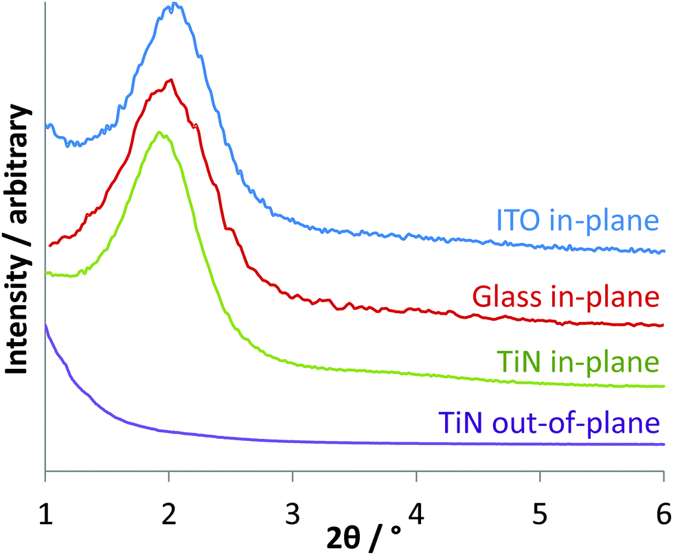 | ||
| Fig. 1 In-plane GISAXS patterns of Stöber films grown on glass, ITO and TiN, and out-of-plane GISAXS of a film grown on TiN. | ||
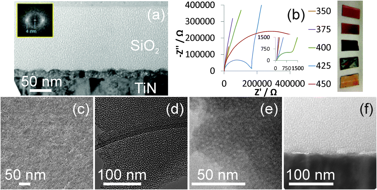 | ||
| Fig. 2 Top row shows a cross-section of a Stöber silica film deposited on TiN after surfactant removal by heating to 450 °C and (inset) fast Fourier transform (a), and Nyquist EIS plots of TiN films heated to various temperatures (b) accompanied by photographs of the same films. Bottom row shows an He-ion micrograph showing the open pores at the surface (c), under-focus (d) and in-focus (e) TEM images of a film after Soxhlet extraction and heating in air to 350 °C, and a cross section TEM image of the TiN/SiO2 interface of a similar film (f). | ||
Film heating is useful to ensure a high degree of condensation of the silica network and high temperature treatment of the mesoporous silica films is required to remove the surfactant template and reveal the open porosity. However heating at 450 °C oxidises the TiN surface. We investigated the thermal stability of TiN in air by heating samples to a range of temperatures (heated at 0.5 °C min−1 and maintained 5 h). Fig. 2 shows that the colour of the TiN films developed with heating temperature, with films only darkening slightly to a copper colour at 350 °C but becoming much darker at 400 or 425 °C and then returning to a lighter colour than the starting film at 450 °C, presumably due to a thick transparent oxide layer. EIS experiments with a nBu4NBF4/acetonitrile electrolyte were used to test the ease of charge transfer at the surface. All films exhibited an uncompensated solution resistance of ∼70 Ω, but as the treatment temperature was increased features corresponding to an interface (the semicircles in Fig. 2) became apparent at temperatures of 400 °C and above. The charge transfer resistance associated with this interface increased from 1.6 kΩ at 400 °C to 167 kΩ at 425 °C and 550 kΩ at 450 °C. It was determined that films could not be heated above 375 °C without a major effect on the surface conductivity of the TiN film. Hence a Soxhlet extraction with acidified ethanol was applied for 6 h to remove as much template as possible, then the films were heated to 350 °C in air for 5 h. Direct measurement of the carbon content in these films is complicated by their thickness, as they are too thin to be good EDX samples but XPS might miss carbon content below the top ∼10 nm. However the C![[thin space (1/6-em)]](https://www.rsc.org/images/entities/char_2009.gif) :Si ratio could be obtained by using EDX with a low (5 kV) accelerating voltage to avoid break through to the silicon substrate. After simple washing and drying the C:Si ratio was 1:5.2, but the procedure reduced it to 1:9.6 after Soxhlet extraction and 1:9.3 after firing at 350 °C. This corresponds to 7% C in SiO2 by mass. GISAXS patterns were unchanged by this procedure and TEM images showed an identical pore structure and film thickness to that observed in films simply heated to 450 °C (Fig. 2), but no interface layer between the TiN surface and the silica film was observed in the TEM cross section. The images appear to show unconnected pores, though it should be noted that even in thin TEM sections the sample thickness is much larger than any micropores that might exist in the silica walls.
:Si ratio could be obtained by using EDX with a low (5 kV) accelerating voltage to avoid break through to the silicon substrate. After simple washing and drying the C:Si ratio was 1:5.2, but the procedure reduced it to 1:9.6 after Soxhlet extraction and 1:9.3 after firing at 350 °C. This corresponds to 7% C in SiO2 by mass. GISAXS patterns were unchanged by this procedure and TEM images showed an identical pore structure and film thickness to that observed in films simply heated to 450 °C (Fig. 2), but no interface layer between the TiN surface and the silica film was observed in the TEM cross section. The images appear to show unconnected pores, though it should be noted that even in thin TEM sections the sample thickness is much larger than any micropores that might exist in the silica walls.
He-ion micrographs showed large numbers of open pores at the surface although some of these appear to combine at the surface to produce larger pores. Secondary electron imaging with the helium ion microscope (HIM) benefits from a very high surface sensitivity.37 This is due to the large proportion of secondary electrons generated by the primary beam compared to those generated by the backscattered helium ions, resulting in an image containing information predominately from within the secondary electron escape depth, which is approximately 1 nm.38 Furthermore, the He ion beam is focused to a sub-nm diameter spot on the sample, limiting the interaction volume and resulting in high lateral resolution. This permits the resolution of the ∼2 nm diameter pores in HIM images of the silica films and also provides evidence that the pores are open. If the pores were closed to a depth larger than the secondary electron escape depth (∼1 nm) the imaging signal would originate almost entirely from the filling material and therefore the pores would not be visible.
Some variations in the films can be achieved by additions of ionic species to the sol or by changing the surfactant. For example addition of a 0.025 mol dm−3 concentration of NaHCO3 to the sol produces a film with a stronger in-plane GI-SAXS signal. Further investigation shows this effect is due to a thicker film of ∼400 nm, while the in-focus TEM images showed very similar pore and wall thicknesses. This may be due to pH changes during growth as bicarbonate thermally decomposes, as nitrate (which has the same charge) has no effect. Addition of sulphate or carbonate, which both have a double negative charge, results in a loss of most of the GI-SAXS intensity, suggesting the stronger attraction to the micelle surfaces results in disruption of their ordering.
Mesitylene addition results in the GI-SAXS peak moving to larger d-spacing values due to swelling of the surfactant assemblies, Fig. 3. The largest observed value was with the addition of 31 μl mesitylene to the standard sol recipe as given in the experimental, with a 2θ position of 1.64° resulting in a hexagonal silica lattice parameter of 6.22 Å. However some broadening of the peak is observed at this concentration as the swelling starts to affect the surfactant ordering. Under-focus TEM showed that these films retain a relatively high degree of hexagonal order and the in-focus TEM (Fig. 3) showed a pore size of ∼2.9 nm, an increase of ∼10% over that seen without mesitylene addition. Addition of triisopropylbenzene was observed to increase the observed d-spacing even further, but film quality deteriorated markedly with large numbers of pinholes and cracks appearing.
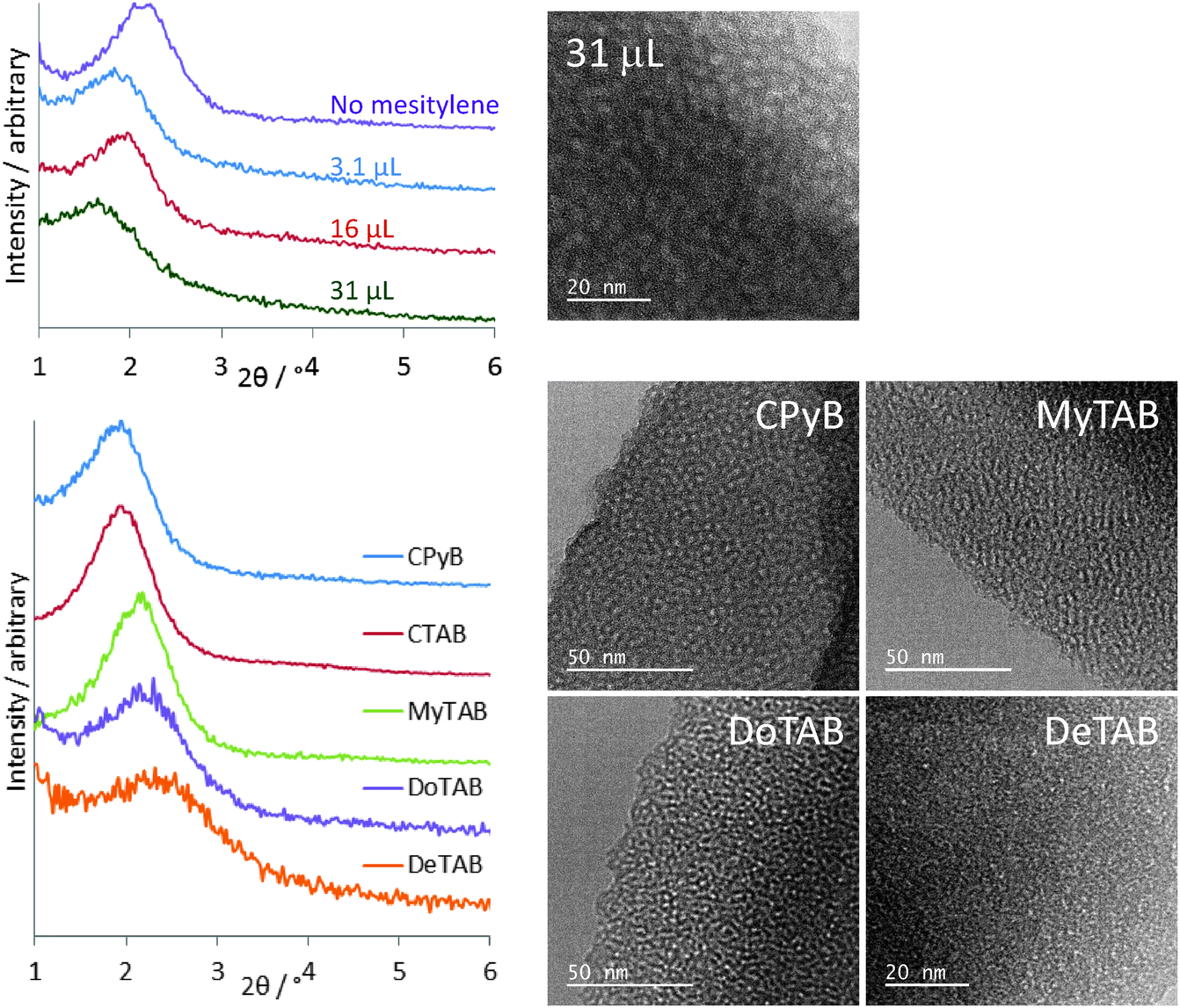 | ||
| Fig. 3 GISAXS plot showing variations in pore spacing with additions of mesitylene (top) or with surfactant variations (bottom). The in-focus TEM of a mesitylene-modified film shows the pore size, whereas the under-focus TEMs with various surfactants show the reduction in pore ordering as the surfactant cation size reduces. | ||
A larger cationic surfactant head group can be used to increase the surfactant pore spacing, so that with cetyltrimethylpyridinium bromide (CPyB) at the same molar concentration as CTAB the main GI-SAXS feature is observed at 1.82°, corresponding to a hexagonal unit cell size of 5.60 Å. Reducing the length of the alkyl chain on the surfactant relative to CTAB results in a progressive shift in the position of the main peak in the GI-SAXS data to lower d-spacing values to 2.12° with MyTAB ([Me3NC14H29][Br]), 2.24° with DoTAB ([Me3NC12H25][Br]) or 2.38° with DeTAB ([Me3NC10H21][Br]). These correspond to hexagonal silica lattice parameters of 5.31, 4.81, 4.55 or 4.29 Å (respectively). The GI-SAXS data in Fig. 3 show a progressive broadening due to a reduction in ordering of the pores with the shorter surfactant chains and hence lower polarity. This change in the degree of ordering is also apparent in the TEM images (Fig. 3). It was also found to be necessary to progressively increase the amount of surfactant used as the chain length was reduced, from 0.10 g CTAB, to 0.22 g with MyTAB, 0.28 g with DoTAB and 0.24 g with DeTAB in order to achieve the most intense GI-SAXS feature. Varying the surfactant affected the intensity of the GI-SAXS feature rather than its position, suggesting the pore size was specific to the surfactant type.
3.2 Electrochemically assisted preparation of aligned mesoporous silica films
The EASA route pioneered by Walcarius and co-workers uses a cathodic potential to induce self-assembly of a surfactant at an electrode surface, and hence requires a conductive substrate. Meanwhile hydroxide ions are produced due to the current passed at the surface of the electrode and these induce condensation of the silica gel around the surfactant assemblies. Deposition onto ITO films at −1.3 V for 20 s, as previously reported,27 resulted in mesoporous silica films with very weak out-of-plane GISAXS features and strong in-plane features at 2.60, 4.36 and 5.00°, that could be indexed as the 10, 11 and 20 reflections of a hexagonal lattice of cylinders with a lattice parameter of 4.01(10) nm. No GISAXS features were observed using the same conditions on TiN substrates, but the same GISAXS features were observed in films deposited at potentials between −1.6 and −2.4 V, with the highest intensities achieved at −1.8 or −2.0 V. Indexing the positions of these reflections led to a measured pore spacing of 4.04(5) nm. Cyclic voltammograms showed two reduction peaks below 1.5 V with both TiN and ITO, and significant current due to electrolyte reduction at 2.0 V, hence it is not obvious why the higher overpotential is required.Films were grown onto substrates in which a region of approx. 1 × 1 cm was immersed into the electrolyte in vertical orientation, whereas previous studies used horizontal substrates with a deposition region defined by a rubber O-ring.27 The disadvantage of our approach is that the current density is known less accurately, but film growth is performed under potentiostatic control and it is the potential that is most critical to achieve an ordered pore structure. The advantage is that very few aggregates due to condensation in the solution are observed on the film surfaces and hence SEM shows films that are smooth over large areas. The deposition time was limited to 5 s as longer periods did result in an increase in the number of aggregates at the surface even in this orientation, in agreement with previous findings on surface precipitation processes in sol–gel electrosynthesis with long deposition times.39 This factor limits the film thickness to the ∼60 nm thickness observed in the TEM (Fig. 5), which also showed hexagonal order of the perpendicularly-aligned pores over much larger domains than found using the Stöber method. He-ion microscopy (Fig. 5) showed films to be relatively smooth and pores to be open at the surface. However to ensure the films are stable it is desirable to apply a heat treatment. Hence the same procedure of Soxhlet extraction with acidified ethanol and heating to 350 °C as described for the Stöber films was applied here. The TEM data in Fig. 5 show that the film thickness and aligned pore structure were retained, and the in focus TEM images indicate a pore size of ∼1.6 nm. The pores appear unconnected in the images, though as with the Stöber films it should be noted that micropores are unlikely to be visible.
The EASA process requires an increase in pH at the electrode surface in order to induce condensation of the silica species in the sol and hence gelation. Replacement of the sodium nitrate electrolyte with KCl reduced the in-plane GISAXS signal of the product significantly despite very similar currents being passed, showing that the presence of nitrate is critical to the operation of this process. Nitrate is often used in electrodeposition of oxides as the standard reduction potential of nitrate ions is higher than that of water,40,41 hence nitrate reduces more readily and will increase the pH locally at the surface of the electrode, e.g.:
| NO3−(aq) + 3H+(aq) + 2e → HNO2(aq) + H2O(l) E⊖ = +0.94 V |
| NO3−(aq) + H2O(l) + 2e → NO2−(aq) + 2OH−(aq) E⊖ = +0.01 V |
It was found to be possible to carry out the EASA process with cetylpyridinium bromide surfactant in the range −1.8 to −2.2 V and, as with the Stöber method this resulted in an increase in the pore spacing (to ∼4.3 nm: 10 reflection observed at 2.35°), but the GISAXS patterns were much broader and the higher d-spacing reflections were not resolved, so the film was much less well ordered. Addition of mesitylene to the mixture to swell the CTAB surfactant resulted in films that retained the film order, with GISAXS peak widths similar to those shown in Fig. 4, but the peaks moved to higher d-spacing (Fig. 6). This is in contrast to a previous report of mesitylene addition to films on ITO, where loss of order was observed.29 With a 0.1:1 mesitylene:CTAB molar ratio the 10, 11 and 20 reflections were observed at 2.28, 4.02 and 4.56° (a = 4.45(3) nm), whereas with 0.5:1 mesitylene:CTAB these reflections were observed at 2.25, 3.92 and 4.54° (a = 4.51(3) nm). In focus TEM images of a film produced with a 0.5:1 mesitylene:CTAB ratio showed the pore size to have expanded to ∼2.4 nm (Fig. 6). As with the Stöber films the use of triisopropylbenzene to swell the CTAB surfactant did result in an increase in pore diameter but also degraded the film quality, with large numbers of pinholes and cracks observed. It was possible to reduce the pore size by substituting the CTAB surfactant with MyTAB, with some increase in GISAXS reflection width. With DoTAB surfactant the GISAXS signal of the films became very weak. This behaviour is similar to that observed on ITO substrates.27
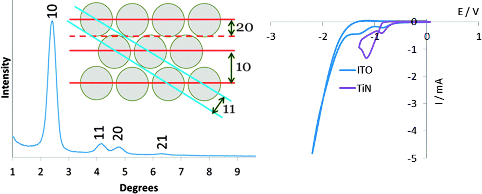 | ||
| Fig. 4 In-plane GISAXS pattern of a mesoporous silica film grown by the EASA method on TiN at −1.8 V for 5 s (left) and cyclic voltammograms of the standard EASA mixture (experimental) with ITO and TiN substrates (right, potential vs. a silver rod pseudo reference, scan rate 100 mV s−1). | ||
 | ||
| Fig. 5 He-ion micrograph of the surface (a), and TEM data showing a cross-section (b) and an under-focus image of the pore order (c) of EASA silica films as prepared. Bottom row shows the TiN–silica boundary (d) and in focus image of a film (e) after template removal by Soxhlet extraction followed by heating at 350 °C. | ||
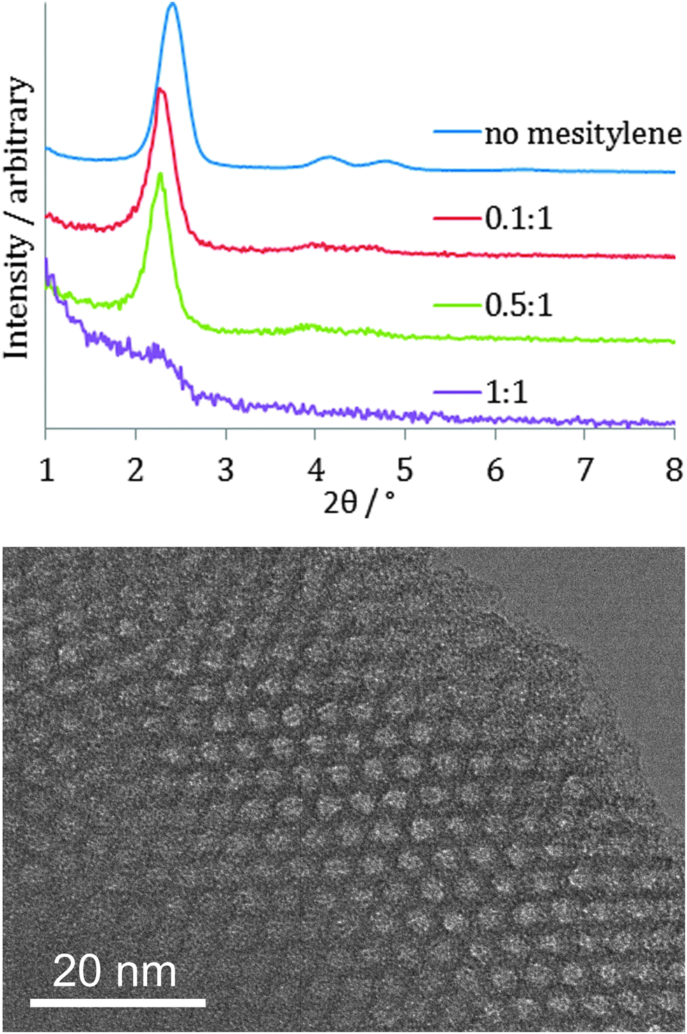 | ||
| Fig. 6 In-plane GI-SAXS patterns of EASA silica films produced with mesitylene:CTAB ratios as shown (top) and in focus TEM image of a film made with 0.5:1 ratio of mesitylene:CTAB (bottom). | ||
4. Conclusions
Both the Stöber and EASA routes employed herein result in small pores aligned perpendicular to the TiN electrode surface with hexagonal pore arrangements. The pores have much longer range order using the EASA route, but this route only allowed a thickness of ∼60 nm without deposition of aggregates onto the surface. Both routes result in porous silica films that are well-adhered to the TiN surface and pores that are open at the top surface so could be used as hosts for nanowire deposition. Despite the use of the same CTAB surfactant the pores are smaller using the EASA route, at around 1.6 nm compared with around 2.6 nm from the Stöber route. In both cases some variation in pore size could be achieved by varying the size of the surfactant molecules or by swelling the surfactant assemblies with mesitylene. These results are expected to extend the scope of applications of these films, especially because of the wider potential window offered by the TiN support in comparison to the previously reported ones for such oriented mesostructures.Acknowledgements
The authors thank EPSRC for funding under the Supercritical Fluids Electrodeposition project (SCFED, EP/I033394/1) and for funding the Smartlab diffractometer (EP/K00509X/1 and EP/K009877/1). Mahboba Hasan is thanked for collecting the EDX data and Veronika Urbanova for assisting with initial EASA depositions. The SCFED Project (http://www.scfed.net) is a multidisciplinary collaboration of British universities investigating the fundamental and applied aspects of supercritical fluids.References
- J. Ke, W. Su, S. M. Howdle, M. W. George, D. Cook, M. Perdjon-Abel, P. N. Bartlett, W. Zhang, F. Cheng, W. Levason, G. Reid, J. Hyde, J. Wilson, D. C. Smith, K. Mallik and P. Sazio, Proc. Natl. Acad. Sci. U. S. A., 2009, 106, 14768–14772 CrossRef CAS PubMed.
- L. Ansari, G. Fagas, J.-P. Colinge and J. C. Greer, Nano Lett., 2012, 12, 2222–2227 CrossRef CAS PubMed.
- X.-L. Qi and S.-C. Zhang, Rev. Mod. Phys., 2011, 83, 1057–1110 CrossRef CAS.
- C. E. Giusca, V. Stolojan, J. Sloan, F. Börrnert, H. Shiozawa, K. Sader, M. H. Rümmeli, B. Büchner and S. R. P. Silva, Nano Lett., 2013, 13, 4020–4027 CrossRef CAS PubMed.
- U.-H. Lee, J. Hyeon Lee, D.-Y. Jung and Y.-U. Kwon, Adv. Mater., 2006, 18, 2825–2828 CrossRef CAS.
- C.-W. Wu, Y. Yamauchi, T. Ohsuna and K. Kuroda, J. Mater. Chem., 2006, 16, 3091–3098 RSC.
- D. Wang, W. L. Zhou, B. F. McCaughy, J. W. Hampsey, X. Ji, Y.-B. Jiang, H. Xu, J. Tang, R. H. Schmehl, C. O'Connor, C. J. Brinker and Y. Lu, Adv. Mater., 2003, 15, 130–133 CrossRef CAS.
- J. Gu, J. Shi, H. Chen, L. Xiong, W. Shen and M. Ruan, Chem. Lett., 2004, 33, 828–829 CrossRef CAS.
- T. Suzuki, H. Miyata, T. Noma and K. Kuroda, J. Phys. Chem. C, 2008, 112, 1831–1836 CAS.
- A. Walcarius, Chem. Soc. Rev., 2013, 42, 4098–4140 RSC.
- M. Etienne, J. Cortot and A. Walcarius, Electroanalysis, 2007, 19, 129–138 CrossRef CAS.
- M. Etienne, Y. Guillemin, D. Grosso and A. Walcarius, Anal. Bioanal. Chem., 2013, 405, 1497–1512 CrossRef CAS PubMed.
- M. Etienne, A. Goux, E. Sibottier and A. Walcarius, J. Nanosci. Nanotechnol., 2009, 9, 2398–2406 CrossRef CAS PubMed.
- G. Herzog, N. A. Vodolazkaya and A. Walcarius, Electroanalysis, 2013, 25, 2595–2603 CrossRef CAS.
- Y. Lu, R. Ganguli, C. A. Drewien, M. T. Anderson, C. J. Brinker, W. Gong, Y. Guo, H. Soyez, B. Dunn, H. H. Huang and J. I. Zink, Nature, 1997, 389, 364–368 CrossRef CAS.
- C. J. Brinker, Y. Lu, A. Sellinger and H. Fan, Adv. Mater., 1999, 11, 579–585 CrossRef CAS.
- V. V. Guliants, M. A. Carreon and Y. S. Line, J. Membr. Sci., 2004, 235, 53–72 CrossRef CAS.
- V. R. Tirumala, R. A. Pai, S. Agarwal, J. J. Testa, G. Bhatnagar, A. H. Romang, C. Chandler, B. P. Gorman, R. L. Jones, E. K. Lin and J. J. Watkins, Chem. Mater., 2007, 19, 5868–5874 CrossRef CAS.
- P. Platschek, A. Keilbach and T. Bein, Adv. Mater., 2011, 23, 2395–2412 CrossRef PubMed.
- G. Ji, Z. Gong, Y. Liu, X. Chang, Y. Du and M. Qamar, Solid State Commun., 2011, 151, 1151–1155 CrossRef CAS.
- Y. Chen, A. Yamaguchi, T. Atou, K. Morita and N. Teramae, Chem. Lett., 2006, 35, 1352–1353 CrossRef CAS.
- A. Keilbach, J. Moses, R. Köhn, M. Döblinger and T. Bein, Chem. Mater., 2010, 22, 5430–5436 CrossRef CAS.
- C. Ottone, K. Bejtka, A. Chiodoni, V. Farías, I. Roppolo, G. Canavese, S. Stassi and V. Cauda, New J. Chem., 2014, 38, 2058–2065 RSC.
- S. Nagarajan, M. Li, R. A. Pai, J. K. Bosworth, P. Busch, D.-M. Smilgies, C. K. Ober, T. P. Russell and J. J. Watkins, Adv. Mater., 2008, 20, 246–251 CrossRef CAS.
- E. K. Richman, T. Brezesinski and S. H. Tolbert, Nat. Mater., 2008, 7, 712–717 CrossRef CAS PubMed.
- A. Walcarius, E. Sibottier, M. Etienne and J. Ghanbaja, Nat. Mater., 2007, 6, 602–608 CrossRef CAS PubMed.
- A. Goux, M. Etienne, E. Aubert, C. Lecomte, J. Ghanbaja and A. Walcarius, Chem. Mater., 2009, 21, 731–741 CrossRef CAS.
- V. Urbanova and A. Walcarius, Z. Anorg. Allg. Chem., 2014, 640, 537–546 CrossRef CAS.
- Y. Guillemin, J. Ghanbaja, E. Aubert, M. Etienne and A. Walcarius, Chem. Mater., 2014, 26, 1848–1858 CrossRef CAS.
- Z. Teng, G. Zheng, Y. Dou, W. Li, C.-Y. Mou, X. Zhang, A. M. Asiri and D. Zhao, Angew. Chem., Int. Ed., 2012, 51, 2173–2177 CrossRef CAS PubMed.
- P. N. Bartlett, D. A. Cook, M. W. George, A. L. Hector, J. Ke, W. Levason, G. Reid, D. C. Smith and W. Zhang, Phys. Chem. Chem. Phys., 2014, 16, 9202–9219 RSC.
- J. M. Blackburn, D. P. Long, A. Cabanas and J. J. Watkins, Science, 2001, 294, 141–145 CrossRef CAS PubMed.
- J. Ke, P. N. Bartlett, D. Cook, T. L. Easun, M. W. George, W. Levason, G. Reid, D. Smith, W. Su and W. Zhang, Phys. Chem. Chem. Phys., 2012, 14, 1517–1528 RSC.
- P. N. Bartlett, D. Cook, C. H. de Groot, A. L. Hector, R. Huang, A. Jolleys, G. P. Kissling, W. Levason, S. J. Pearce and G. Reid, RSC Adv., 2013, 3, 15645–15654 RSC.
- V. S. Smentkowski and C. A. Moore, J. Vac. Sci. Technol., A, 2013, 31, 06F105 Search PubMed.
- M. C. Biesinger, L. W. M. Lau, A. R. Gerson and R. S. C. Smart, Appl. Surf. Sci., 2010, 257, 887–898 CrossRef CAS.
- G. Hlawacek, I. Ahmad, M. A. Smithers and E. S. Kooij, Ultramicroscopy, 2013, 135, 89–94 CrossRef CAS PubMed.
- R. Ramachandra, B. Griffin and D. Joy, Ultramicroscopy, 2009, 109, 748–757 CrossRef CAS PubMed.
- E. Sibottier, S. Sayen, F. Gaboriaud and A. Walcarius, Langmuir, 2006, 22, 8366–8373 CrossRef CAS PubMed.
- N. N. Greenwood and A. Earnshaw, Chemistry of the Elements, Elsevier Butterworth-Heinemann, Oxford, 2nd edn, 1997 Search PubMed.
- G. H. Annal Therese and P. V. Kamath, Chem. Mater., 2000, 12, 1195–1204 CrossRef.
| This journal is © the Owner Societies 2015 |