
 Open Access Article
 This Open Access Article is licensed under a
 Creative Commons Attribution 3.0 Unported Licence
Nonlinear optical imaging of single plasmonic nanoparticles with 30 nm resolution
Anke
Horneber
*a,
Kai
Braun
a,
Jan
Rogalski
a,
Paul
Leiderer
b,
Alfred J.
Meixner
a and
Dai
Zhang
*a
aInstitute of Physical and Theoretical Chemistry, Center for Light-Matter Interaction, Sensors & Analytics, University of Tuebingen, Auf der Morgenstelle 15, Tuebingen, Germany. E-mail: dai.zhang@uni-tuebingen.de; anke.horneber@uni-tuebingen.de; Fax: +49 7071 29-5490; Tel: +49 7071 29-77639
bDepartment of Physics, University of Konstanz, Universitätsstrasse 10, 78457 Konstanz, Germany
First published on 23rd January 2015
Abstract
We show that background free nonlinear optical imaging of Au nanostructures with a resolution down to 30 nm can be achieved. To attain such performance, an ultrafast laser source (110 fs pulse duration) has been integrated into a parabolic mirror assisted scanning near-field optical microscope. Combining nonlinear hyperspectral imaging and the simultaneously obtained topography, the setup allows one to directly correlate/assign locations with nonlinear signals originating from either second harmonic generation or two-photon excitation processes. The contrast mechanisms of the far-field background free nonlinear optical image are discussed based on the different tip–sample coupling schemes and the selective excitation of the plasmonic modes.
1. Introduction
In the last few decades apertureless scanning optical near-field microscopy (apertureless SNOM) became a popular tool to investigate optical signals with a sub λ/2 resolution.1 Based on localized plasmonic resonances and the ‘lightning rod’ effect, immense near-fields are generated at the apex of a sharp metal tip.2 This confinement of the electromagnetic field is beneficial both for breaking the diffraction-limited optical resolution, and for enhancing the optical detection sensitivity down to even single molecules.3Compared to linear optical processes, the generation of nonlinear optical signals requires a much higher threshold regarding the power of the excitation field. For example, second harmonic generation (SHG) scales nonlinearly as |χ(2)|2I2, where χ(2) is the 2nd order nonlinear susceptibility and I is the laser intensity. Two-photon photoluminescence (2PPL) is a nonlinear process described by χ(2) and the rate of absorption of energy is quadratically dependent on the laser intensity.4 Therefore the combination of nonlinear optical microscopy and SNOM allows us to obtain high optical contrast with nanometer optical resolution.5 Within the last few decades several nonlinear techniques have been integrated to aperture SNOMs using glass fiber tips. Combined with the pump–probe technique, SNOMs have been used to study ultrafast dynamics in quantum wells, wires and dots of inorganic semiconductors.6–8 Sanchez et al. imaged fragments of photosynthetic membranes and J-aggregates based on 2PPL signals with an optical resolution of about 30 nm using apertureless SNOM.9 Subsequently, tip enhanced coherent anti stokes microscopy (CARS),10 second harmonic generation,11 multiplex sum frequency,12 and four wave mixing13 have been demonstrated. Furthermore, the development of a home-made SNOM setup using commercial cantilever-based hollow-pyramid probes coupled to femtosecond pulses has been reported, investigating nonlinear optical signals from Au triangles and nanorods.14 For implementing very short fs-pulses, the chromatic dispersion of fiber tips may lead to different propagation velocity of the various spectral components and in turn to a lower group velocity for higher spectral components within the medium and a considerable pulse broadening.15 Using gold tips the problem can be circumvented. Furthermore, the near field at the tip apex should not be created by propagation of the light through the tip or a plasmon along the tip shaft, but by plasmonic excitation close to the apex such that the phase matching of short laser pulses is loosened. Additionally in apertureless SNOM, the coupling between the sharp tip apex and the substrate provides a highly confined electric field (gap-mode),16 acting as a nanometer-sized light source for the excitation of a variety of optical processes. Therefore, apertureless SNOM combined with ultrasfast laser technique is a promising tool to study the photophysical properties of plasmonic nanoparticles, even at the single object level.
In this paper we report our recent progresses in constructing an apertureless SNOM that was combined with an ultra-short laser source (110 fs, 774 nm). The excitation scheme is optimized regarding the polarization conditions and the laser focus element. This technique was applied to achieve high-resolution optical imaging of Au nanostructures based on both linear PL, 2PPL, and SHG signals. The origins of the optical contrast are discussed with respect to the local dielectric environment, and the different plasmonic modes.
2. Experiment and discussion
2.1 fs-SNOM configuration
The optical path of the fs-SNOM is shown in Fig. 1. A femtosecond laser was coupled into the setup in order to produce ultrashort pulses (∼110 fs, 774 nm, 90 MHz). The laser light is expanded by telescope 1 and afterwards delivered to a home-built mode converter (MC). This element consists of four quarters of lambda half plates which are carefully aligned and assembled according to Quabis.17 Each quarter of the MC rotates the polarization of the incoming TEM00 laser beam so that it points outwards, perpendicular to the k-vector in each segment. After passing through a pinhole in telescope 2, the undesired higher order polarization modes and scattered light are filtered out to obtain a homogeneous, radially polarized doughnut mode. The radially polarized laser beam is reflected using a 50![[thin space (1/6-em)]](https://www.rsc.org/images/entities/char_2009.gif) :50 non-polarizing beam splitter. Afterwards the beam travels perpendicular towards a parabolic mirror with a numerical aperture of 0.998 in air. The parabolic mirror serves both as a focusing element for the laser beam and for efficient signal collection.18 It furthermore allows a homogeneous broad-band spectral response, a minimal chromatic aberration, and a distinct electric distribution in its focus. The radially polarized laser beam focused by a parabolic mirror leads to a dominant out-of-plane electric field in the laser focus.19,20 A home built scanning head places a sharp electrochemically etched gold tip into the laser focus. The optically excited tip acts as a nanometer sized local light source for the sample excitation and as an antenna to transmit the near field optical signal back to the far field regime. Near-field measurements were performed by statically positioning the tip inside the laser focus and scanning the sample below. To control the tip–sample distance we used a shear force feedback mechanism.21 Throughout the SNOM experiment, a phase shift of maximum 5 degrees, corresponding to a distance of about 3 nm, was maintained. The optical signals from the sample are collected by the parabolic mirror, transmitted through the beam splitter, and afterwards sent to telescope 3 to reduce the beam size. After passing through the laser filter, the frequency shifted part of the light is sent to the detectors. The optical signals can be directed to a spectrometer (600 grating) equipped with a thermoelectrically cooled CCD-camera for spectral analysis. For optical imaging, the signals can be sent to two single photon detection avalanche photodiodes (APD): one is sensitive (>40%) in the red spectral range (490–875 nm) for linear photoluminescence imaging and the other one in the blue range (360–840 nm) for the 2PPL and SHG imaging.
:50 non-polarizing beam splitter. Afterwards the beam travels perpendicular towards a parabolic mirror with a numerical aperture of 0.998 in air. The parabolic mirror serves both as a focusing element for the laser beam and for efficient signal collection.18 It furthermore allows a homogeneous broad-band spectral response, a minimal chromatic aberration, and a distinct electric distribution in its focus. The radially polarized laser beam focused by a parabolic mirror leads to a dominant out-of-plane electric field in the laser focus.19,20 A home built scanning head places a sharp electrochemically etched gold tip into the laser focus. The optically excited tip acts as a nanometer sized local light source for the sample excitation and as an antenna to transmit the near field optical signal back to the far field regime. Near-field measurements were performed by statically positioning the tip inside the laser focus and scanning the sample below. To control the tip–sample distance we used a shear force feedback mechanism.21 Throughout the SNOM experiment, a phase shift of maximum 5 degrees, corresponding to a distance of about 3 nm, was maintained. The optical signals from the sample are collected by the parabolic mirror, transmitted through the beam splitter, and afterwards sent to telescope 3 to reduce the beam size. After passing through the laser filter, the frequency shifted part of the light is sent to the detectors. The optical signals can be directed to a spectrometer (600 grating) equipped with a thermoelectrically cooled CCD-camera for spectral analysis. For optical imaging, the signals can be sent to two single photon detection avalanche photodiodes (APD): one is sensitive (>40%) in the red spectral range (490–875 nm) for linear photoluminescence imaging and the other one in the blue range (360–840 nm) for the 2PPL and SHG imaging.
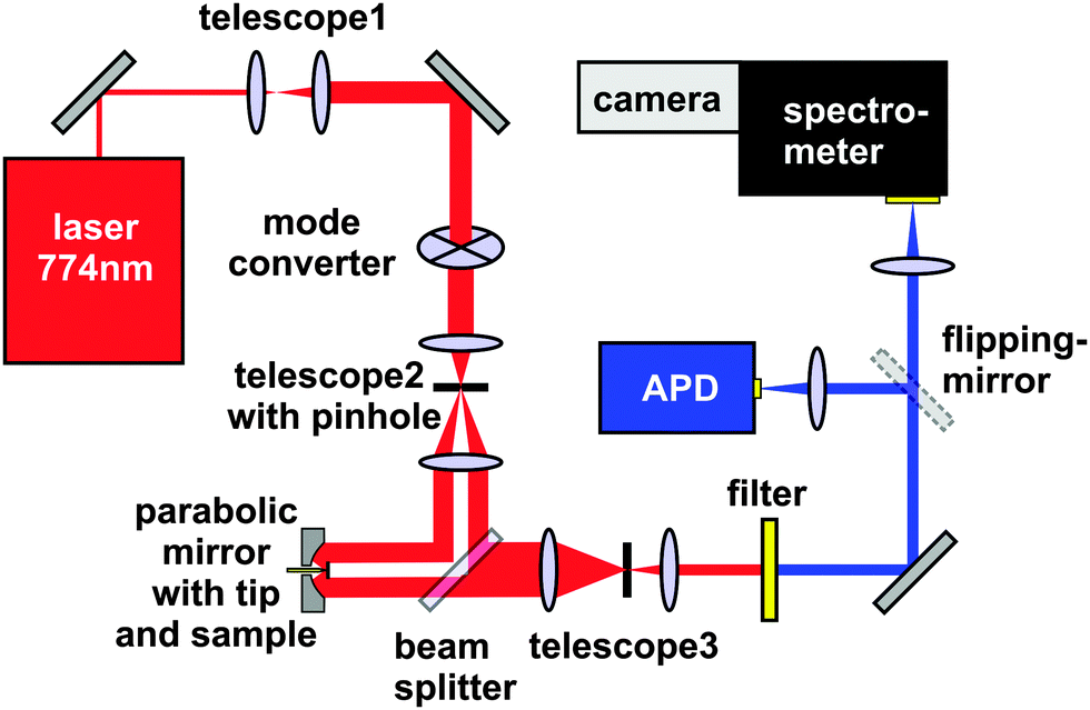 | ||
| Fig. 1 Scheme of the optical path of the home-built fs-SNOM. | ||
2.2 Far-field linear and nonlinear imaging
The Au nanostructures were fabricated by colloid lithography.22 A diluted colloidal suspension of polystyrene beads with a diameter of 922 nm was used to form a self-assembled monolayer by drying on the substrate, a commercially available silicon wafer that is covered by a thin layer of native oxide. Onto this layer of polystyrene colloids Au was evaporated, which also filled the voids in between the colloids. Periodically ordered nanotriangles, also called Fischer patterns,23 can be produced by removing the colloid layer with a piece of adhesive tape. A SEM image of the investigated sample can be seen in Fig. 2(a). Fig. 2(b) shows an optical image of such a sample based on the red-shifted one photon photoluminescence produced by the linear excitation process. The linear photoluminescence excited by the 774 nm laser is caused by an intraband excitation process.24 Periodic intensity variations can be observed for the hexagonally arranged structure. Nevertheless, a clear correlation between the intense photoluminescence signals with the positions of the Au nanotriangles cannot be resolved. Besides linear photoluminescence, nonlinear optical signals are also observed from the sample, as shown in Fig. 2(c). The spectrum clearly shows the frequency doubled signal at 387 nm. From 450 nm to 675 nm, the steeply increasing signals are mainly composed of the X- and the L-bands of 2PPL, which are well known from transitions near the X and L symmetry points at the first Brillouin zone of crystalline Au.25 The nonlinear signal is very weak. Therefore, the peak at 428 nm from the ambient light can also be seen. The peak at 530 nm is due to the intensity modulation (inhomogeneous transmission) of the beam splitter. Fig. 2(d) shows a nonlinear optical image which has been simultaneously obtained with Fig. 2(b) from the same sample region. The observed triangles within the pattern have sizes around 300 nm, which are close in size to the dimensions of the exciting focus. Due to the lack of intensity and optical resolution, the hexagonal arrangement of the triangles cannot be revealed by this optical measurement. | ||
| Fig. 2 (a) SEM image of the Au nanotriangle structures. (b) Confocal optical imaging of the Au nanotriangle structures based on the red-shifted photoluminescence. (c) A nonlinear spectrum from the Au nanotriangle structures. Integration time: 60 s. (d) Confocal optical imaging based on the blue-shifted optical signal. Excitation power: 1 mW. | ||
2.3 Near-field linear and nonlinear imaging
Fig. 3 shows near-field experiments performed with the fs-SNOM, where the sample is scanned through the focus of a radially polarized vector beam and the sharp Au tip is kept statically in the focus.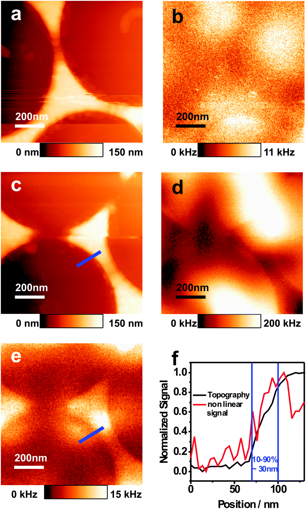 | ||
| Fig. 3 (a) The topography of Au nanotriangles. (b) The simultaneously obtained high-resolution optical image based on the linear photoluminescence, dominated by the signal from the far-field excitation. (c) The topography from other Au nanotriangles. (d) The simultaneously obtained high-resolution optical image based on the linear photoluminescence. The image is dominated by elastically scattered laser light which is not totally blocked by the filter. (e) The high-resolution optical image based on the nonlinear optical signal which is simultaneously obtained with (d). (f) The optical resolution was estimated to be around 30 nm taking the 10–90% criterion into account. The blue lines indicate the positions where line-profiles of the optical and topographical data were taken. | ||
The simultaneously obtained topography, linear photoluminescence, images from an fs-SNOM experiment is shown in Fig. 3(a) and (b), respectively. A further measurement is presented in Fig. 3 including the topography in (c), an image of linear and elastically scattered light in (d) and a nonlinear photoluminescence image in (e). The topographies show nanotriangles with heights of about 150 nm. In the linear photoluminescence SNOM image (Fig. 3(b)) (signals with wavelengths longer than 800 nm), the contours of the nanotriangles are not clearly resolved due to overlapping with some strong optical signal. The linear signal in Fig. 2(d) shows, however, highly resolved negative contrast against some very bright regions in the background. In contrast to this image, the nonlinear SNOM image shown in Fig. 3(e) (signals from a spectral range of 375–650 nm) of the same triangles presents a positive contrast with position specific optical signal variations. The optical resolutions of the nonlinear-SNOM are evaluated using a 10–90% criterion.26 The positions of the line-profiles for the optical resolution evaluation are marked in Fig. 3(c) and (e) as blue lines. The resolution was determined to be about 30 nm.
The validity and quality of high resolution optical imaging based on the linear signal are very sensitive to the interferences from the far-field excitation, as well as the instrument conditions. Fig. 3(b) and (d) are two examples to demonstrate such influences. The linear signal in Fig. 3(b) originates from several contributions. The bright regions which do not correlate with the position of the nanotriangles are dominated by the Au photoluminescence excited by the far-field laser focus (as shown in Fig. 2(b)), giving rise to a far-field ‘cross-talk’ to the near-field generated signals.27 The convolution of the linear photoluminescence signals with the periodically ordered nanotriangles – especially those with sizes smaller than the far-field focus – form highly ordered optical patterns. However, it has to be noted that these patterns cannot be directly correlated with the actual locations of the nanotriangles. As demonstrated in Fig. 3(b), some of the bright spots from the far-field excitation are not present at the Au nanotriangles, rather appearing at the positions of the polystyrene beads before they were peeled off from the substrate. Besides these very bright regions, linear photoluminescence correlating with the nanotriangle positions is generated from the Au tip–Au triangle nanogap, which is the actual component contributing to the high-resolution photoluminescence image.
The appearance of the negative optical contrast in Fig. 3(d) is not a ‘quenching effect’. In this experiment elastically scattered laser light leaked from the excitation to the detector, giving strong far-field interference. Additionally the tip acts as a scattering-type of antenna for the scattered light. When the Au tip scans above the Au nanotriangles, a Au–Au nanogap is formed which absorbs the excitation laser producing e.g. photoluminescence signals. Therefore, at these positions less laser light is scattered as compared to the situation when the tip scans above the inert Si substrate. Thus, a highly resolved negative contrast on the gold nanotriangle appears in Fig. 3(d). In Fig. 3(e), the nonlinear optical signals from the nanotriangles are visible as positive contrast since they depend on the incident field to the power of four. The field strength within the confocal far-field focus is considerably weak as compared to the field in the Au tip–substrate nanogap. Thus the far-field artefacts are overpowered by the nonlinear near-field signal leading to an intense and positive nonlinear signal contrast in Fig. 3(e). In short, Fig. 3(b), (d) and (e) clearly demonstrate the effective reduction of far-field induced interference in fs-SNOM high-resolution imaging.
Besides the contrast between the near-field and the minimized far-field excited optical signals, there are at least two other processes that account for the optical contrast shown in Fig. 3(e). The first process is caused by the different coupling between the excited tip apex with either the Au nanotriangles or the Si substrate. As has been reported in the state-of-the-art,28 as well as from our own former work,29 the excitation and emission from the tip–substrate gap mode are greatly influenced by the tip size, the gap distance and the dielectric properties of the substrate. The Si substrate has a high dielectric constant in the visible range, which is less effectively polarized by the excited Au tip than a Au substrate. In contrast, Au nanoparticles with small gaps are well-known to generate higher field enhancement due to increased plasmonic coupling.30–32 The Au tip–Au nanotriangle junction with a ca. 3 nm gap distance results in a ‘bowtie’ antenna configuration that is parallel to the optical axis of the optical microscope. Therefore, the dominant out-of-plane electric field (parallel to the optical axis of the microscope) in the focus of a radially polarized beam could excite the gap-mode effectively, leading to a highly confined near-field in the 3 nm nanogap. This efficient coupling leads to a high near-field enhancement, which is able to initiate the nonlinear optical process more effectively than the Au–Si interaction.
The second process likely originates from the presence of different plasmonic modes at the nanotriangles. These modes give rise to nonlinear signal variations even within the same single nanotriangle. This aspect will be discussed in the next section.
2.4 Near-field nonlinear hyperspectral imaging
In our SNOM configuration, the scanning tip has a fixed geometry and material properties, whilst the substrate consists of nanostructures of different size and materials (Au or Si). The differences in the light matter interaction are therefore dominantly influenced by changes in the substrate properties. Hyperspectral imaging provides the possibility of obtaining location-correlated optical signals, as well as avoiding instrument drift induced data-collection complexity. We collected 7 × 8 spectra and the topographical information (96 × 112 pixels) simultaneously. Using this technique the spectral information can be easily assigned to the different locations.Fig. 4 shows the nonlinear excitation of a Au tip alone as well as a topography-correlated 2PPL and SHG signal imaging from a nanotriangle. An optical image recorded by raster scanning a Au tip through the laser focus is shown in Fig. 4(a). The corresponding nonlinear spectrum shown in Fig. 4(b) is composed of a sharp SHG peak at 387 nm and a broad band starting from 550 nm to the cutting edge of the filter at 670 nm. The nonlinear signal from the tip alone – both SHG and 2PPL – has been reported before.24,33 Notably, even though all Au tips produce linear photoluminescence, not all of them give a recordable nonlinear optical signal (SHG or nonlinear photoluminescence). For example, the tip used for the following hyperspectral SNOM imaging does not show recordable nonlinear signal when it was positioned in the focus alone. In Fig. 4(c) the topography of two nanotriangles is shown. On the upper nanotriangle, there is also some surface roughness visible caused by the sample fabrication process. In Fig. 4(d) two nonlinear optical spectra taken from defined locations are shown. The blue spectrum shows the signal originating from one nanotriangle. The other spectrum is obtained from the substrate. Two peaks, peak 1 and peak 3, are caused by the signal modulation of the inhomogeneous transmission of the beam splitter. Peak 2 is the real signature from the 2PPL emission. Fig. 4(e) shows the 2PPL imaging of the two nanotriangles based on the integrated spectral intensity of peak 2. Fig. 4(f) shows the distribution of the SHG signal. In Fig. 4(g) and (h) the position variation of the peak 2 2PPL peak and the SHG peak is depicted, respectively. The SHG position stays very constant, which serves as a reference experiment to verify the stability of the laser. Besides the peak position variations, the 2PPL and SHG intensities also seem to be correlated with the different locations on the nanotriangles, as seen in Fig. 4(e) and (f). The strongest signals are emitted directly at the gold nanotriangles and in close vicinity. At the lower left corner residues from the fabrication process are situated which are yielding a SHG and 2PPL signal as well. This signal has about half the intensity of the signal coming from the upper gold triangle.
 | ||
| Fig. 4 Hyperspectral SNOM mapping of the nanotriangles. (a) The nonlinear optical image when a sharp Au tip scans through the laser focus. (b) A spectrum collected from an excited Au tip, (c) topography of nanotriangles, (d) two nonlinear spectra obtained from the Au-tip–nanotriangle junction at two different positions (marked in blue and green colours) that are indicated in image (c) by the blue and green circles, (e) SNOM 2PPL intensity map, (f) SNOM SHG intensity map, (g) peak 2 position variation map, (h) SHG peak variation map. The white doted matrix (7 × 8) marks the positions where tip-enhanced nonlinear spectra were taken. Spectral integration time: 60 s. | ||
A clear difference between the two spectra in Fig. 4(d) is the spectral profile variation, where the 2PPL has a rather prominent peak shape centred at around 620 nm. Its peak position varies from location to location by about 50 nm as shown in Fig. 4(g), which is in contrast to the stable SHG. Previous electron energy loss experiments on Ag nanoprisms revealed that there are three plasmonic modes present: a corner mode (ω = 1078 nm), an edge mode (ω = 670 nm) and a center mode (ω = 496 nm).34 Moving from the rim to the centre of the nanotriangle, the 2PPL peaks averagely shift from about 594 nm to 600 nm, which somewhat correlate with the gradually increased plasmonic modes energy observed in the Ag nanoprism. To find out the influences of different plasmonic modes on the spectral profile of 2PPL, we need to firstly consider the excitation and emission mechanisms in Au. The photoluminescence from bulk gold was first reported as being caused by the radiative recombination of the excited electrons of the sp band with d-band holes with a very low quantum yield (10−6).35 Later more efficient photoluminescence emission was observed from roughened noble metal film surfaces caused by the plasmon enhancement of the radiative transitions.36 Intensive debates about the roles that (localized) plasmons play in the photoluminescence emission of gold are still going on; plasmon-enhanced interband transitions37 and radiative decay from excited particle plasmons38,39 have both been reported. Plasmonic effects influence not only the linear PL process of nanoparticles, but also the 2PPL generation. Though not yet universally observed, many reports have shown that the plasmonic resonance can ‘shape’ the 2PPL emission spectrum. 2PPL spectra from nanoparticles follow the plasmonic resonances of nanoparticles.40 For example, it has been reported that the localized surface plasmons in nanoparticles offer an additional decay channel, which can compete with the direct recombination of excited electrons with holes.41
Fig. 5 is therefore proposed to explain the observed plasmonic effect related 2PPL excitation scheme. As the first step, two photons are absorbed by the Au nanostructures. The radiative decay of the excited electrons from the sp band back to the d band gives rise to the normal X- or L-2PPL emission (step 2). However when plasmonic modes are present, at energies close to the sp band, the excited electrons have the opportunity to decay nonradiatively transferring energy to the plasmonic modes (step 3). In SNOM measurements with nanotriangles, much depends on the location of the Au tip, the coupling of the tip and the substrate can be different due to geometrical (at the edge or center of the nanotriangles) and dielectric media related (on Si or Au) factors. The excited plasmonic modes decay radiatively (step 4) giving rise to 2PPL emission, which closely follows the energy and the distribution of the plasmonic modes. Due to the presence of plasmonic modes of different energies, the 2PPL emission is shaped accordingly with different peak positions, giving rise to the peak shift from approximately 600 nm at the nanotriangle rim to 594 nm in the centre.
 | ||
| Fig. 5 A solid state model explanation of the plasmonic related 2PPL emission from nanostructures. Step 1: two-photon excitation from the d band to the sp band. Step 2: interband relaxation producing 2PPL photons. Step 3: energy transfer from the excited sp band to the plasmonic modes of slightly different energies. Step 4: radiative decays from the plasmonic modes to the d band giving rise to 2PPL of slightly different energies. | ||
3. Conclusions
We have demonstrated the nolinear optical imaging of single plasmonic nanostructure with an optical resolution of 30 nm using a home-built fs-SNOM. High resolution imaging of nanotriangles with linear or nonlinear excitation was performed simultaneously and correlated with the nanotriangle topography. The reduced and negative contrasts shown in the linear photoluminescence images are largely due to ‘cross-talk’ from the far-field optical signal which superimposes on the near-field image. Due to the second order effect, a clear positive contrast was observed from the nonlinear optical image. This contrast originates from (1) the weaker coupling between the Au tip and Si substrate as compared to the Au tip and the Au nanotriangles and (2) different plasmonic modes at the nanotriangles. Using hyperspectral imaging which allows us to obtain correlated topography and spectral information at the same time, we are able to obtain insights into the ‘shaping’ effect of localized plasmonic modes on the 2PPL spectral profile. A theoretical model was suggested to explain the possible mechanisms of the plasmonic ‘shaping’ effect. With this work, we would like to contend that the SNOM technique combined with an ultrafast laser source opens up an efficient way to investigate a broad spectrum of light-matter interactions. With the possibility of integrating life time imaging, we believe that this technique will also find its popularity in investigating the strength of light-matter interactions in hybrid systems.Acknowledgements
The financial support from DFG through the ‘priority program -SPP1391’ is acknowledged. We thank Frank Wackenhut for very fruitful discussions.Notes and references
- U. Dürig, D. W. Pohl and F. Rohner, J. Appl. Phys., 1986, 59, 3318–3327 CrossRef PubMed.
- Y. Inouye and S. Kawata, Opt. Lett., 1994, 19, 159–161 CrossRef CAS.
- R. Zhang, Y. Zhang, Z. C. Dong, S. Jiang, C. Zhang, L. G. Chen, L. Zhang, Y. Liao, J. Aizpurua, Y. Luo, J. L. Yang and J. G. Hou, Nature, 2013, 498, 82–86 CrossRef CAS PubMed.
- J. D. Bhawalkar, G. S. He and P. N. Prasad, Rep. Prog. Phys., 1996, 59, 1041 CrossRef CAS.
- S. Kawata and P. Verma, Chimia, 2006, 60, 770–776 CrossRef CAS.
- J. Levy, V. Nikitin, J. M. Kikkawa, A. Cohen, N. Samarth, R. Garcia and D. D. Awschalom, Phys. Rev. Lett., 1996, 76, 1948–1951 CrossRef CAS.
- S. Smith, N. C. R. Holme, B. Orr, R. Kopelman and T. Norris, Ultramicroscopy, 1998, 71, 213–223 CrossRef CAS.
- T. Guenther, C. Lienau, T. Elsaesser, M. Glanemann, V. M. Axt, T. Kuhn, S. Eshlaghi and A. D. Wieck, Phys. Rev. Lett., 2002, 89, 057401 CrossRef.
- E. J. Sánchez, L. Novotny and X. S. Xie, Phys. Rev. Lett., 1999, 82, 4014–4017 CrossRef.
- T. Ichimura, N. Hayazawa, M. Hashimoto, Y. Inouye and S. Kawata, Phys. Rev. Lett., 2004, 92, 220801 CrossRef.
- A. V. Zayats, T. Kalkbrenner, V. Sandoghdar and J. Mlynek, Phys. Rev. B: Condens. Matter Mater. Phys., 2000, 61, 4545–4548 CrossRef CAS.
- R. D. Schaller, J. C. Johnson, K. R. Wilson, L. F. Lee, L. H. Haber and R. J. Saykally, J. Phys. Chem. B, 2002, 106, 5143–5154 CrossRef CAS.
- P. Stefano, D. Matthias and N. Lukas, J. Opt. A: Pure Appl. Opt., 2009, 11, 114030 CrossRef.
- M. Celebrano, P. Biagioni, M. Zavelani-Rossi, D. Polli, M. Labardi, M. Allegrini, M. Finazzi, L. Duò and G. Cerullo, Rev. Sci. Instrum., 2009, 80, 033704 CrossRef PubMed.
- R. Paschotta, Encyclopedia of Laser Physics and Technology, John Wiley & Sons, 2008 Search PubMed.
- P. Vasa, C. Ropers, R. Pomraenke and C. Lienau, Laser Photonics Rev., 2009, 3, 483–507 CrossRef PubMed.
- S. Quabis, R. Dorn and G. Leuchs, Appl. Phys. B: Lasers Opt., 2005, 81, 597–600 CrossRef CAS PubMed.
- C. Stanciu, M. Sackrow and A. J. Meixner, J. Microsc., 2008, 229, 247–253 CrossRef CAS PubMed.
- M. Sackrow, C. Stanciu, M. A. Lieb and A. J. Meixner, ChemPhysChem, 2008, 9, 316–320 CrossRef CAS PubMed.
- D. Zhang, X. Wang, K. Braun, H.-J. Egelhaaf, M. Fleischer, L. Hennemann, H. Hintz, C. Stanciu, C. J. Brabec, D. P. Kern and A. J. Meixner, J. Raman Spectrosc., 2009, 40, 1371–1376 CrossRef CAS PubMed.
- K. Karrai and R. D. Grober, Appl. Phys. Lett., 1995, 66, 1842–1844 CrossRef CAS PubMed.
- F. Burmeister, C. Schäfle, B. Keilhofer, C. Bechinger, J. Boneberg and P. Leiderer, Adv. Mater., 1998, 10, 495–497 CrossRef CAS.
- U. C. Fischer and H. P. Zingsheim, J. Vac. Sci. Technol., 1981, 19, 881–885 CrossRef CAS.
- M. R. Beversluis, A. Bouhelier and L. Novotny, Phys. Rev. B: Condens. Matter Mater. Phys., 2003, 68, 115433 CrossRef.
- Z. Guan, S. Li, P. B. S. Cheng, N. Zhou, N. Gao and Q.-H. Xu, ACS Appl. Mater. Interfaces, 2012, 4, 5711–5716 CAS.
- S. W. Smith, The Scientist & Engineer's Guide to Digital Signal Processing, California Technical Pub, 1997 Search PubMed.
- D. Sadiq, J. Shirdel, J. S. Lee, E. Selishcheva, N. Park and C. Lienau, Nano Lett., 2011, 11, 1609–1613 CrossRef CAS PubMed.
- M. B. Raschke and C. Lienau, Appl. Phys. Lett., 2003, 83, 5089–5091 CrossRef CAS PubMed.
- D. Zhang and A. J. Meixner, in Handbook of Spectroscopy, Wiley-VCH Verlag GmbH & Co. KGaA, 2014, pp.911–940 Search PubMed.
- L. Gunnarsson, T. Rindzevicius, J. Prikulis, B. Kasemo, M. Käll, S. Zou and G. C. Schatz, J. Phys. Chem. B, 2004, 109, 1079–1087 CrossRef PubMed.
- P. K. Jain and M. A. El-Sayed, J. Phys. Chem. C, 2008, 112, 4954–4960 CAS.
- B. M. Reinhard, M. Siu, H. Agarwal, A. P. Alivisatos and J. Liphardt, Nano Lett., 2005, 5, 2246–2252 CrossRef CAS PubMed.
- A. Hartschuh, M. R. Beversluis, A. Bouhelier and L. Novotny, Philos. Trans. R. Soc., A, 2004, 362, 807–819 CrossRef CAS PubMed.
- J. Nelayah, M. Kociak, O. Stéphan, N. Geuquet, L. Henrard, F. J. García de Abajo, I. Pastoriza-Santos, L. M. Liz-Marzán and C. Colliex, Nano Lett., 2010, 10, 902–907 CrossRef CAS PubMed.
- A. Mooradian, Phys. Rev. Lett., 1969, 22, 185–187 CrossRef CAS.
- G. T. Boyd, Z. H. Yu and Y. R. Shen, Phys. Rev. B: Condens. Matter Mater. Phys., 1986, 33, 7923–7936 CrossRef CAS.
- M. B. Mohamed, V. Volkov, S. Link and M. A. El-Sayed, Chem. Phys. Lett., 2000, 317, 517–523 CrossRef CAS.
- E. Dulkeith, T. Niedereichholz, T. A. Klar, J. Feldmann, G. von Plessen, D. I. Gittins, K. S. Mayya and F. Caruso, Phys. Rev. B: Condens. Matter Mater. Phys., 2004, 70, 205424 CrossRef.
- A. Tcherniak, S. Dominguez-Medina, W.-S. Chang, P. Swanglap, L. S. Slaughter, C. F. Landes and S. Link, J. Phys. Chem. C, 2011, 115, 15938–15949 CAS.
- M. D. Wissert, K. S. Ilin, M. Siegel, U. Lemmer and H.-J. R. Eisler, Nano Lett., 2010, 10, 4161–4165 CrossRef CAS PubMed.
- F. Wackenhut, A. V. Failla and A. J. Meixner, J. Phys. Chem. C, 2013, 117, 17870–17877 CAS.
| This journal is © the Owner Societies 2015 |