
 Open Access Article
 This Open Access Article is licensed under a Creative Commons Attribution-Non Commercial 3.0 Unported Licence
Metal–organic Kagome lattices M3(2,3,6,7,10,11-hexaiminotriphenylene)2 (M = Ni and Cu): from semiconducting to metallic by metal substitution†
Shuang
Chen
,
Jun
Dai
and
Xiao Cheng
Zeng
*
Department of Chemistry and Nebraska Center for Materials and Nanoscience, University of Nebraska-Lincoln, Lincoln, Nebraska 68588, USA. E-mail: xzeng1@unl.edu
First published on 21st January 2015
Abstract
Motivated by recent experimental synthesis of a semiconducting metal–organic graphene analogue (J. Am. Chem. Soc., 2014, 136, 8859), i.e., Ni3(2,3,6,7,10,11-hexaiminotriphenylene)2 [Ni3(HITP)2], a new Kagome lattice, Cu3(HITP)2, is designed by substituting the coordination of Ni by Cu. Such substitution results in interesting changes in electronic properties of the M3(HITP)2 bulk and two-dimensional (2D) sheets. In Ni3(HITP)2, each Ni atom adopts the dsp2 hybridization, forming a perfect 2D conjugation, whereas in Cu3(HITP)2, each Cu atom adopts the sp3 hybridization, resulting in a distorted 2D sheet. The M3(HITP)2 bulks, assembled from M3(HITP)2 sheets via both strong π–π interaction and weak metal–metal interaction, are metallic. However, the 2D Ni3(HITP)2 sheet is a semiconductor with a narrow band gap whereas the 2D Cu3(HITP)2 sheet is a metal. Remarkably, both the 2D M3(HITP)2 Kagome lattices possess Dirac bands in the vicinity of the Fermi level. Additional ab initio molecular dynamics simulations show that both sheets exhibit high thermal stability at elevated temperatures. Our theoretical study offers new insights into tunability of electronic properties for the 2D metal–organic frameworks (MOFs).
Introduction
Two-dimensional (2D) functional materials, including graphene,1 graphene derivatives,2 layered metal chalcogenides,3 and 2D covalent-organic frameworks (COFs),4,5 have attracted intensive attention owing to their novel electronic, optical, and mechanical properties for future device applications. Graphene, a single layer of sp2-bonded carbon atoms in a honeycomb lattice, is a 2D carbon allotrope. However, the lack of a bandgap limits its device application.6 Graphene derivatives possess a bandgap but at the expense of decreased charge carrier mobility.2 Two new classes of 2D materials, transition metal chalcogenides7–10 and COFs,11,12 are also viewed as potential alternatives to graphene derivatives since the transition metal chalcogenides can be easily produced in large areas with controlled thicknesses13 while the organic COFs can be chemically modified.11 However, the chemical functionalization of metal chalcogenides is difficult and the carrier mobility of COFs tends to be depressed due to the reduction of in-plane conjugation resulting from COFs own flexibility or the presence of functional groups in the building blocks. A new class of metal–organic frameworks (MOFs) assembled from square-planar metal ions and aromatic organic moieties, such as o-semiquinone,14 dithiolene,15,16 and iminotriphenylene,17 has emerged recently to combine advantages of both inorganic and organic materials. These MOFs exhibit high electrical conductivity due to full charge delocalization in the 2D plane or π–π stacking along the stacked columns.14–17 Interestingly, a previous theoretical investigation predicted that the 2D π-conjugated nickel-bis-dithiolene monolayer may possess a non-zero bandgap and even behave as a topological insulator.18 Thus, these 2D MOFs could be potential candidates for future electronics.In this study, we select the recently synthesized semiconducting MOF, Ni3(2,3,6,7,10,11-hexaiminotriphenylene)2 [Ni3(HITP)2],17 as a model system. Our goal is to investigate the effect of substitution of coordinated metal ions, e.g. from Ni to Cu in the MOF, on the structural and electronic properties of the MOF bulks and 2D sheets. We note that these 2D M3(HITP)2 sheets exhibit the Kagome-lattice pattern. By changing every coordinated metal site, the metal coordination (dsp2 → sp3 hybridization), the geometry of in-plane network (planar → buckled), and the electronic properties (semiconducting → metallic) of 2D M3(HIPT)2 sheets are modified as shown in Fig. 1. Our theoretical work suggests high tunability of 2D MOFs with exotic electronic properties by metal substitution.
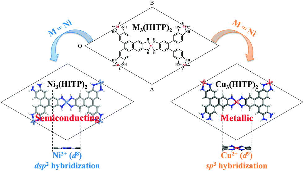 | ||
| Fig. 1 Illustration of 2D MOFs M3(HITP)2 (M = Ni and Cu). By substituting Ni with Cu, the coordination of the metal site, geometry within the 2D conjugated plane, and electronic properties of the M3(HITP)2 sheets are notably modified. | ||
Computational details
Density functional theory (DFT) methods implemented in the Vienna Ab Initio Simulation Package (VASP 5.3.5)19,20 are used to optimize the three-dimensional (3D) M3(HITP)2 (M = Ni and Cu) bulks and 2D sheets. Before the DFT optimization of the periodic systems, the molecular units of M3(HITP)2 (see ESI,† Fig. S1) are initially optimized at the level of B3LYP/6-31G(d), implemented in the Gaussian 09 software package.21 The natural-bond-orbital (NBO) analysis22 at the same level is also employed to gain insight into the coordination of M3(HITP)2. Based on the optimized molecular units, the periodic 3D bulks and 2D sheets are then constructed. For the initial lattice constants of 3D bulk M3(HITP)2 (M = Ni and Cu), we refer to the predicted Ni3(HITP)2 crystal structure in the previous work.17 We set the unit cell parameters c = 6.6 Å, α = β = 90°, and γ = 60°, and then place the second M3(HITP)2 layer on top of the first layer but with a parallel shift relative to the first layer by 1.8 Å along the a axis, b axis, or both a and b axes, respectively, to generate three possible crystalline structures (see ESI,† Fig. S2). For optimization of each 2D M3(HITP)2 sheet, a vacuum layer of 30 Å is added so that the interlayer interactions are negligible. Note that for possible stacking arrangements of M3(HITP)2 layers, here we consider only the above three configurations since comprehensive experimental/theoretical analyses by powder X-ray diffraction (PXRD) and Ni K-edge extended X-ray absorption fine structure (EXAFS) measurements of Ni3(HITP)2 crystals combined with DFT calculations of the potential energy surface (PES) generated by different translations between two Ni3(HITP)2 layers have already been reported.17 More specifically, by comparing simulated PXRD patterns of several possible stacking arrangements with the experimental PXRD pattern, Sheberla et al. ruled out the staggered configuration.17 From additional EXAFS analysis, they found that the Ni3(HITP)2 crystal should exhibit a slipped-parallel orientation rather than the eclipsed orientation.17 Finally, with the help of DFT calculations of 82 crystals with different ab-plane displacements and a fixed interlayer separation along c, they showed that the fully eclipsed structure was energetically unfavorable and the slipped-parallel orientation wherein one Ni3(HITP)2 layer was slipped relative to a neighboring layer by about 1.8 Å along the a or b vectors gave the lowest energy on the PES.17For computation of electronic properties (including band structures, density of states (DOS), and charge density distribution), the Perdew–Burke–Ernzenhof (PBE)23 form for the exchange–correlation functional within the framework of the generalized gradient approximation (GGA) is employed. Grimme's correction (D3)24 is also adopted to account for weak van der Waals interactions within the organic materials. The electron–ion interaction is described by the projector augmented wave (PAW) potentials25,26 with an energy cutoff of 500 eV. For geometry optimization, the total energy change is set to less than 10−5 eV and the magnitude of the largest force acting on the atoms is set to less than 0.02 eV Å−1. The Brillouin zones are sampled using a 2 × 2 × 6 or 4 × 4 × 1 k-point mesh in the Monkhorst–Pack scheme for 3D bulks or 2D sheets, respectively.27 For more accurate calculations of electronic properties of M3(HITP)2 bulks or sheets, a twice denser k-point mesh is used, and the convergence criterion of self-consistent field (SCF) computation is set to 10−6 eV. For the M3(HITP)2 3D bulks and 2D sheets, the spin-polarized computation is also performed to examine their magnetic properties. In addition, the effects of spin–orbit coupling (SOC) are considered to examine the possible non-collinear magnetic states of the Cu3(HITP)2 sheet, as well as to estimate the opening of a small bandgap in the Kagome bands of the 2D M3(HITP)2 sheets.
We also examined thermal stability of both 2D M3(HITP)2 sheets using ab initio molecular dynamics (AIMD) simulations at elevated temperatures. The AIMD simulations are performed using the QUICKSTEP program implemented in the CP2K software package.28 Within the framework of the Kohn–Sham formulation of DFT and the Gaussian plane-wave (GPW) method,29 the core electrons are described by the Goedecker–Teter–Hutter (GTH) normconserving pseudopotential,30,31 and the wave functions of valence electrons are expressed by the combination of the polarized double-ζ quality Gaussian basis32 and a plane-wave basis set (with an energy cutoff of 330 Ry). The dispersion-corrected PBE-D3 method is selected. For the Cu3(HITP)2 sheet, the spin-polarized computation is applied. The AIMD simulations are performed in the constant-volume and constant-temperature ensemble with the temperature controlled at 500 K and 1000 K, respectively, for each sheet. For each temperature, ten ps simulation is carried out with the time step of 1.0 fs.
Results and discussion
3D metallic M3(HITP)2 bulks
The previous experimental study showed that the Ni3(HITP)2 crystal favored the slipped-parallel orientation between neighboring Ni3(HITP)2 layers.17 In the same work, the computational study (based on PBE-D2 functional) also suggested that the 3D structure of Ni3(HITP)2 in which one layer was shifted laterally with respect to the neighboring layer by about 1.8 Å along the a axis, or b axis, or both ab axes has the lowest energy.17 Here, our DFT geometry optimization of both 3D Ni3(HITP)2 and Cu3(HITP)2 bulks indicates that the shift of the second layer in the unit cell along the b axis gives rise to the lowest-energy structure among the three possible crystal structures (see ESI,† Fig. S2). Based on the lowest-energy crystal structures, the computed electronic band structures, DOS, and the charge density isosurface for the bands crossing the Fermi level are presented in Fig. 2. As shown in Fig. 2a and c, both 3D Ni3(HITP)2 and Cu3(HITP)2 crystals are metallic with a band crossing the Fermi level along M(1/2, 0, 0)–L(1/2, 0, 1/2) and H(2/3, 1/3, 1/2)–K(2/3, 1/3, 0). The predicted metallic property of Ni3(HITP)2 is consistent with the excellent bulk and thin film conductivity of 2 and 40 S cm−1 obtained from the two-probe and van der Pauw electrical measurements, respectively.17 Moreover, the band structures exhibit relatively strong dispersions within the M–L or H–K region (see Fig. 2a and c), indicating strong π–π interaction between metal–organic sheets along their stacking direction (c axis). We also plot the charge density isosurface of the bands crossing the Fermi level for the M3(HTIP)2 bulks in Fig. 2b and d. These bands are mainly contributed from the out-of-plane Ni-d, C-p, and N-p delocalized states (no contribution from H atoms), consistent with interlayer metal–metal and π–π interactions. Indeed, according to the cell parameters of M3(HTIP)2 bulks (ESI,† Fig. S2), the interlayer distance between two M3(HTIP)2 sheets is about 3.3 Å, which is within the van der Waals interaction distance of 2D conjugated carbon layers, and the closest Ni⋯Ni and Cu⋯Cu distances between two sheets are 3.809 Å and 3.952 Å, respectively, indicating strong π–π interaction and weak metal–metal (d–d) interaction between the two sheets. | ||
| Fig. 2 Computed band structures, DOS (a and c) and charge-density isosurface of bands crossing the Fermi level (b and d) of 3D M3(HITP)2 (M = Ni and Cu) bulks, based on the spin-nonpolarized PBE-D3 calculations. The Fermi level is marked by a thin blue line. The bands crossing the Fermi level for Ni3(HITP)2 and Cu3(HITP)2 are highlighted in red and blue lines, respectively. The value of the charge density isosurface is 0.005 e Bohr−3. | ||
2D semiconducting Ni3(HITP)2 sheets versus metallic Cu3(HITP)2 sheets
The reduced dimensionality from 3D M3(HTIP)2 bulks to 2D sheets leads to a significant change in the electronic properties. As shown in Fig. 3a and d, the Ni3(HTIP)2 sheet is a semiconductor with a small bandgap of 0.13 eV, while the Cu3(HTIP)2 sheet is still metallic. For the Ni3(HTIP)2 sheet (Fig. 3a), its valence band maximum (VBM) is located at the K point while its conduction band minimum (CBM) is located at the Γ point, suggesting Ni3(HTIP)2 is an indirect semiconductor. The direct bandgap at the Γ point is about 0.23 eV, slightly larger than the indirect bandgap. Since the Kohn–Sham bandgaps generally underestimate the physical bandgaps, the HSE06 functional33–35 is also employed to compute the band structures of the Ni3(HTIP)2 sheet. As shown in (ESI†) Fig. S3, the occupied valence bands computed from the HSE06 functional exhibit a downward shift while the unoccupied conduction bands show an upward shift, compared to the PBE-D3 bands. The shift of the VBM and CBM is quite small, and the HSE06 functional results in an indirect bandgap of 0.20 eV and a direct bandgap of 0.19 eV at the Γ point, close to the PBE-D3 bandgaps. As indicated by the charge-density isosurface of the highest occupied valence band (HOVB) and of the lowest unoccupied conduction band (LUCB) for the Ni3(HTIP)2 sheet in Fig. 3b and of the band crossing the Fermi level for the Cu3(HTIP)2 sheet in Fig. 3e, these bands stem mainly from the M-d, C-p, and N-p states (no contribution from H atoms). Furthermore, the projected density of states (PDOS) of these bands (ESI,† Fig. S4) show that both 2D MOFs exhibit typical π-conjugated characteristics, since their PDOS near the Fermi level are almost fully contributed by the pz orbitals of C and N atoms as well as the delocalized d orbitals of metal atoms. For the delocalized d orbitals, only the dyz and dxz orbitals of Ni atoms provide contribution to both the HOVB and LUCB. In addition, the contributions of dyz and dxz to the HOVB or LUCB of the Ni3(HITP)2 sheet are nearly the same as one another. For the Cu3(HTIP)2 sheet, the four d orbitals of Cu atoms contribute to the band crossing the Fermi level except dz2. Furthermore, from the NBO analysis, we know that the Ni atoms in the Ni3(HITP)2 sheet adopt the dsp2 hybridization to form the square-planar geometry with the organic moieties. The Ni3(HITP)2 sheet has a perfectly 2D conjugated plane, and its HOVB and LUCB show π-bonding and π-antibonding characteristics, respectively. On the other hand, each Cu atom adopts the sp3 hybridization. The coordination geometry of Cu atoms in the Cu3(HITP)2 sheet is slightly distorted, and thus the 2D sheet is slightly buckled. | ||
| Fig. 3 Computed band structures, DOS (a and d) and charge-density isosurface (b and e) obtained from the spin-nonpolarized PBE-D3 calculation, and a zoom-in view of Kagome bands with SOC gaps, Δ1 and Δ2, (c and f) obtained from the SOC calculations of 2D M3(HITP)2 (M = Ni and Cu) sheets. The Fermi level is marked by a thin blue line. The HOVB and LUCB of the Ni3(HITP)2 sheet and the band crossing the Fermi level of the Cu3(HITP)2 sheet are highlighted in red or blue lines, respectively. The isosurface value for charge density is 0.005 e Bohr−3. | ||
A previous tight-binding model predicted that typical Kagome bands consist of one flat band above two Dirac bands.36 The 2D metal–organic nickel-bis-dithiolene (Ni3C12S12) lattice also exhibits similar Kagome bands with three spin degenerated bands above the Fermi level.18 The bandgap of the Dirac bands is about 13.6 meV (Δ1), while the bandgap between the flat band and the top branch of the Dirac bands is about 5.8 meV (Δ2).18 Moreover, the Ni3C12S12 Kagome lattice was predicted to be a 2D organic topological insulator due to the intrinsic spin–orbit coupling of Ni ions.18 Compared to the Ni3C12S12 Kagome lattice, the Ni3(HTIP)2 sheet has different aromatic organic moieties from dithiolene to iminotriphenylene with a larger conjugated C core and different coordinated organic sites from the S atom to the NH group. As shown in Fig. 3c, the Ni3(HITP)2 sheet has similar Kagome bands above the Fermi level as Ni3C12S12. The higher flat band meets the top branch of the Dirac bands at the Γ point with the SOC gap (Δ2) of 34.0 meV. The bandgap of Dirac bands is 8.7 meV (Δ1). With substitution of the metal sites, the band structures of the Cu3(HITP)2 sheet near the Fermi level become quite different from those of Ni3(HTIP)2 (see Fig. 3d). As shown in Fig. 3f, the Cu3(HITP)2 sheet still has three degenerate Kagome bands and the same Dirac bandgap (Δ1) as Ni3(HITP)2. Differently, the higher flat band meets the top branch of the Dirac bands at the M point with a quite small SOC gap (Δ2 = 4.6 meV). Similar to Ni3C12S12, the Fermi level of the M3(HTIP)2 sheets is not located in the SOC gap. Hence, doping two (or four) electrons per unit cell in the M3(HITP)2 sheet is needed. For Ni3C12S12, the doping concentration was predicted to be about 2 × 1014 cm−2.18 The M3(HITP)2 sheets have a longer lattice constant (about 22 Å) than the lattice constant of Ni3C12S12 (about 15 Å). So less doping concentration, estimated to be about 8 × 1013 cm−2, is needed for the M3(HITP)2 sheets. For real device application, the electrostatic gating is required to achieve the doping effect.
Lastly, our AIMD simulations show that both 2D metal–organic Kagome lattices exhibit quit high thermal stability. Snapshots of M3(HITP)2 sheets at 500 K and 1000 K after 10 ps AIMD simulations are shown in Fig. 4. Clearly, the overall framework of both 2D MOFs become more flexible as the temperature increases. Moreover, compared to the initial average coordinated M–N (M = Ni or Cu) bond lengths, both Ni–N and Cu–N bonds become longer as the temperature increases. The change in Cu–N bonds is slightly larger than that of Ni–N bonds. Nevertheless, both metal–organic networks still keep their structures even at 1000 K. It appears that their thermal stability is better than 2D organic COFs because the COFs are typically stable only up to 700 K.12
 | ||
| Fig. 4 Snapshots of 2D M3(HITP)2 (M = Ni and Cu) sheets at 500 K and 1000 K after 10 ps AIMD simulations. rM–N (M = Ni and Cu) indicates the average bond length, and the initial rM–N is taken from optimized configurations. | ||
Conclusions
The metal substitution results in interesting changes in both geometry and electronic properties of 3D M3(HITP)2 bulks and 2D sheets. For Ni3(HITP)2, each Ni atom adopts the dsp2 hybridization, leading to a perfect 2D conjugation. However, for Cu3(HITP)2, each Cu atom adopts the sp3 hybridization to form a specific square-grid coordination geometry, leading to a distorted 2D sheet. The M3(HITP)2 bulks, assembled from M3(HITP)2 sheets via both strong π–π interaction and weak metal–metal interaction, are metallic. For 2D MOFs, the Ni3(HITP)2 sheet is a semiconductor with a narrow bandgap, while the Cu3(HITP)2 sheet is metallic. Importantly, the M3(HITP)2 sheets possess the Dirac bands near the Fermi level. Moreover, 2D MOFs show higher thermal stability than 2D COFs. As such, the M3(HITP)2 sheets can be promising 2D materials in place of pure 2D organic materials. With other metal ions or organic moieties as the 2D metal–organic Kagome lattices by design, new electronic or even exotic magnetic properties may be uncovered for future device applications.Acknowledgements
We thank Dr Wei Fa for valuable discussions. This work was supported by the National Science Foundation (NSF) through the Nebraska Materials Research Science and Engineering Center (MRSEC) (grant No. DMR-1420645) and by the University of Nebraska Holland Computing Center.Notes and references
- K. S. Novoselov, V. I. Fal'ko, L. Colombo, P. R. Gellert, M. G. Schwab and K. Kim, Nature, 2012, 490, 192 CrossRef CAS PubMed.
- X. Huang, Z. Yin, S. Wu, X. Qi, Q. He, Q. Zhang, Q. Yan, F. Boey and H. Zhang, Small, 2011, 7, 1876 CrossRef CAS PubMed.
- Q. H. Wang, K. Kalantar-Zadeh, A. Kis, J. N. Coleman and M. S. Strano, Nat. Nanotechnol., 2012, 7, 699 CrossRef CAS PubMed.
- X. Feng, X. Ding and D. Jiang, Chem. Soc. Rev., 2012, 41, 6010 RSC.
- S.-Y. Ding and W. Wang, Chem. Soc. Rev., 2013, 42, 548 RSC.
- A. H. C. Neto, F. Guinea, N. M. R. Peres, K. S. Novoselov and A. K. Geim, Rev. Mod. Phys., 2009, 81, 109 CrossRef.
- M. Chhowalla, H. S. Shin, G. Eda, L.-J. Li, K. P. Loh and H. Zhang, Nat. Chem., 2013, 5, 263 CrossRef PubMed.
- C. N. R. Rao, H. S. S. R. Matte and U. Maitra, Angew. Chem., Int. Ed., 2013, 52, 13162 CrossRef CAS PubMed.
- L. Kou, C. Tang, Y. Zhang, T. Heine, C. Chen and T. Frauenheim, J. Phys. Chem. Lett., 2012, 3, 2934 CrossRef CAS.
- L. Kou, T. Frauenheim and C. Chen, J. Phys. Chem. Lett., 2013, 4, 1730 CrossRef CAS.
- J. W. Colson and W. R. Dichtel, Nat. Chem., 2013, 5, 453 CrossRef CAS PubMed.
- J.-J. Adjizian, P. Briddon, B. Humbert, J.-L. Duvail, P. Wagner, C. Adda and C. Ewels, Nat. Commun., 2014, 5, 5842 CrossRef PubMed.
- A. L. Elías, N. Perea-López, A. Castro-Beltrán, A. Berkdemir, R. Lv, S. Feng, A. D. Long, T. Hayashi, Y. A. Kim, M. Endo, H. R. Gutiérrez, N. R. Pradhan, L. Balicas, T. E. Mallouk, F. López-Urías, H. Terrones and M. Terrones, ACS Nano, 2013, 7, 5235 CrossRef PubMed.
- M. Hmadeh, Z. Lu, Z. Liu, F. Gándara, H. Furukawa, S. Wan, V. Augustyn, R. Chang, L. Liao, F. Zhou, E. Perre, V. Ozolins, K. Suenaga, X. Duan, B. Dunn, Y. Yamamto, O. Terasaki and O. M. Yaghi, Chem. Mater., 2012, 24, 3511 CrossRef CAS.
- T. Kambe, R. Sakamoto, K. Hoshiko, K. Takada, M. Miyachi, J.-H. Ryu, S. Sasaki, J. Kim, K. Nakazato, M. Takata and H. Nishihara, J. Am. Chem. Soc., 2013, 135, 2462 CrossRef CAS PubMed.
- J. Cui and Z. Xu, Chem. Commun., 2014, 50, 3986 RSC.
- D. Sheberla, L. Sun, M. A. Blood-Forsythe, S. Er, C. R. Wade, C. K. Brozek, A. Aspuru-Guzik and M. Dincă, J. Am. Chem. Soc., 2014, 136, 8859 CrossRef CAS PubMed.
- Z. F. Wang, N. Su and F. Liu, Nano Lett., 2013, 13, 2842 CrossRef CAS PubMed.
- G. Kresse and J. Furthmüller, Comput. Mater. Sci., 1996, 6, 15 CrossRef CAS.
- G. Kresse and J. Furthmüller, Phys. Rev. B: Condens. Matter Mater. Phys., 1996, 54, 11169 CrossRef CAS.
- M. J. Frisch, G. W. Trucks and H. B. Schlegel, et al., Gaussian 09, Revision D.01, Gaussian, Inc., Wallingford, CT, 2013 Search PubMed.
- E. D. Glendening, A. E. Reed, J. E. Carpenter and F. Weinhold, NBO, Version 3.1.
- J. P. Perdew, K. Burke and M. Ernzerhof, Phys. Rev. Lett., 1996, 77, 3865 CrossRef CAS.
- S. Grimme, J. Antony, S. Ehrlich and H. Krieg, J. Chem. Phys., 2010, 132, 154104 CrossRef PubMed.
- P. E. Blöchl, Phys. Rev. B: Condens. Matter Mater. Phys., 1994, 50, 17953 CrossRef.
- G. Kresse and D. Joubert, Phys. Rev. B: Condens. Matter Mater. Phys., 1999, 59, 1758 CrossRef CAS.
- H. J. Monkhorst and J. D. Pack, Phys. Rev. B: Solid State, 1976, 13, 5188 CrossRef.
- J. VandeVondele, M. Krack, F. Mohamed, M. Parrinello, T. Chassaing and J. Hutter, Comput. Phys. Commun., 2005, 167, 103 CrossRef CAS PubMed.
- G. Lippert, J. R. Hutter and M. Parrinello, Mol. Phys., 1997, 92, 477 CrossRef CAS.
- M. Holz, X.-A. Mao, D. Seiferling and A. Sacco, J. Chem. Phys., 1996, 104, 669 CrossRef CAS PubMed.
- C. Hartwigsen, S. Goedecker and J. Hutter, Phys. Rev. B: Condens. Matter Mater. Phys., 1998, 58, 3641 CrossRef CAS.
- J. VandeVondele and J. Hutter, J. Chem. Phys., 2007, 2007, 114105 CrossRef PubMed.
- J. Heyd, G. E. Scuseria and M. Ernzerhof, J. Chem. Phys., 2003, 118, 8207 CrossRef CAS PubMed.
- J. Heyd and G. E. Scuseria, J. Chem. Phys., 2004, 121, 1187 CrossRef CAS PubMed.
- J. Heyd, G. E. Scuseria and M. Ernzerhof, J. Chem. Phys., 2006, 124, 219906 CrossRef PubMed.
- E. Tang, J.-W. Mei and X.-G. Wen, Phys. Rev. Lett., 2011, 106, 236802 CrossRef.
Footnote |
| † Electronic supplementary information (ESI) available: The M3(HITP)2 building blocks, possible M3(HITP)2 crystals, HSE06 band structure, DOS of 2D Ni3(HITP)2 sheets, and PDOS of M3(HITP)2 sheets. See DOI: 10.1039/c4cp05328a |
| This journal is © the Owner Societies 2015 |