
 Open Access Article
 This Open Access Article is licensed under a
 Creative Commons Attribution 3.0 Unported Licence
Confinement of massless Dirac fermions in the graphene matrix induced by the B/N heteroatoms†
Shansheng
Yu
*ab,
Weitao
Zheng
a,
Zhimin
Ao
*bc and
Sean
Li
b
aDepartment of Materials Science, College of Materials Science and Engineering, Jilin University, Changchun, 130012, China. E-mail: yuss@jlu.edu.cn; wtzheng@jlu.edu.cn
bDepartment of Materials Science and Engineering, the University of New South Wales, 2052, Australia. E-mail: sean.li@unsw.edu.au
cSchool of Chemistry and Forensic Science, University of Technology, Sydney, 2007, Australia. E-mail: zhimin.ao@uts.edu.au
First published on 9th January 2015
Abstract
In this work, the systems are constructed with the defect lines of B–B or N–N dimers embedded in a graphene matrix using density functional theory. It is found that the Dirac-cone dispersions appear at the Fermi level in the bands introduced by the B or N heteroatom, linear B–B or N–N dimers, demonstrating that the carrier mobility is ∼106 m s−1 which is comparable with that of the pristine graphene. Most importantly, such dimer lines act as the quasi-1-D conducting nanowires whose charge carriers are confined around the linear defects in these dimers while the charge carriers in pristine graphene are dispersed two-dimensionally. Such systems suggest that heteroatoms in graphene can indeed contribute to the Dirac cone. In addition, the type of carriers (p-type or n-type) can be manipulated using the B or N heteroatoms, respectively. This will greatly enrich the electronic properties of Dirac semimetals.
Introduction
As microelectronic devices continue to diminish in size to achieve higher speeds, the design parameters of the devices have pushed the currently used materials to the limits. To maintain the rate of device shrinkage without scarifying the overall performance goals, the conventional field effect transistors in semiconductor devices will eventually reach a natural performance limit associated with the fundamental issues in energy loss, heat dissipation etc.1 Graphene has been recognized as a potential candidate to replace the silicon for a next-generation material in the semiconductor technology.2–4 Based on k·p theory,5 the performance of semiconductor devices can be improved significantly by reducing the effective mass of electrons. The intrinsic band structure of pristine graphene has linear energy dispersion at the Fermi level, implying that the charge carriers are 2-D massless fermions. It indicates that the carriers in graphene have an effective ‘speed of light’ of ∼106 m s−1. In order to engineer the graphene transistor into the integrated circuits, it is important to develop graphene containing heteroatoms besides carbon with interesting electronic properties compared to pristine graphene to improve the performance of graphene-based electronics significantly.By only changing the geometric structure of graphene, the electronic properties can be tailored. However, the Dirac point disappears when the perfect bipartite symmetry of the honeycomb lattice in 2-D graphene is broken, for example, in 0-D quantum graphene dots and 1-D graphene nanoribbons.6,7 Thus, in order to develop the high quality devices, Prof. Louie and his co-workers created a graphene superlattice with an external periodic potential,8 which leads to the anisotropic behaviours of massless Dirac fermions depending on the potential barrier height and width. Although this route can control the propagation of the charge carrier along a particular direction, the distribution of spatial charge carriers is not confined to the narrow space. The structure of the 5-5-8 line defect, which is formed by stitching the two graphene domains with a C–C dimer line, has been prepared experimentally.9 Such a linear defect can act as a metallic nanowire in graphene. It raised a question of whether this nanowire can be further developed to tunnel the charge carriers by enhancing their mobility significantly.
Recently, some other 2-D graphene allotropes possessing Dirac cones can be created according to electronic structure calculations.10,11 It is believed that the symmetry of the hexagonal lattice is not the fundamental requirement for the Dirac dispersion of carriers. Although 2-D graphynes containing heteroatoms are also exhibited to feature Dirac points in their band structure, such heteroatoms do not contribute to the Dirac cone at all.10 A question of fundamental interest is whether a heteroatom can indeed contribute to the Dirac cone. Doping B or N into graphene is commonly used to modulate the electronic and transport properties of graphene.12 This is because the B or N atom has one less or more electron than the C atom with comparable atomic size. For B/N doped graphene, the band gap could be opened since the density of states near the Fermi level is suppressed.13 Such a B or N dopant in graphene can be regarded as an acceptor or donor dopant, thus a p-/n-type doping behaviour is exhibited while maintaining considerably good mobility and conductivity.14,15 Therefore, B/N doped graphene has shown a range of applications in p-/n-type graphene-based field-effect transistors,16 electrochemical biosensors,17 and so on. The structure of the 5-5-8 line defect in graphene is easily attacked by an N dopant.18,19 The magnetization can be induced or annihilated by suitable doping, and the magnetic moment depends on the doping sites. In this work, we investigated the electronic structures in the systems that the linear defect of C–C dimers is replaced by the B–B and N–N dimers, respectively, using density functional theory (DFT). The holes or electrons introduced by the B or N dopants can be attracted by the ionic B− or N+ and also the coordinated zigzag edges,12 thus pulling away the localized states near the Fermi level from the lower energy zone. Such a phenomenon is associated with the correlation effect and the Dirac character to re-appear at the Fermi level. Due to the confinement effect, it opens the band-gap of the rest of the part of graphene, thus confining the new carriers (holes or electrons) to move along the linear defects with ultra-high mobility.
Methods and models
In this work, the calculations of geometrical optimization and electronic bands were conducted using DFT using the DMOL3 code.20 In the DFT calculations, the all-electron Kohn–Sham wavefunctions were expanded in the double numerical polarized atomic orbital basis, and the generalized gradient approximation with Perdew–Burke–Ernzerhof describing the exchange and correlation energy was employed.21 A self-consistent field procedure was done until the change in energy was less than 10−6 Hartree, and the geometrical optimization of the structure was done with an energy convergence criterion of 10−5 Hartree. For band structure calculations, the sampling was carried out with 0.001 Å−1 between consecutive k-points on the reciprocal space path. Calculations using the CASTEP22 code were performed for electronic orbitals induced by the bands close to the Fermi level at the low-energy zone (range about from ∼−0.4 eV to ∼0.4 eV), containing occupied and unoccupied orbitals. In addition, the VASP23 code was also employed to understand the behavior of electronic orbitals at the Dirac point.It is well known that the standard DFT underestimates the band gap of semiconductors and insulators substantially. The so-called screened exchange, or the sX-LDA scheme, may be required to understand the properties of semiconductors and insulators. Their calculations are exceedingly expensive in terms of memory usage and time. However, for semimetal materials (e.g. graphene, graphyne, janugraphene, chlorographene and other graphene allotropes),10,11,24 Dirac cones could be predicted using standard DFT calculations. All stable structures in this work were achieved by sufficient relaxation including cell lattices. The band structures with and without relaxing cell lattices were also compared in the ESI,† Fig. S1. The difference between their energy bands is tiny, which indicates that such electronic structures originate in a special atomic arrangement.
The dynamic stability of new structures had also been examined by the molecular dynamics using the DMOL3 code.20 The constant temperature and volume (NVT) ensemble was used with time steps of 3 fs for a total simulation time of 3 ps at 300 K.
In order to investigate the energy band structure, the system with C–C dimer lines periodically embedded in graphene was illustrated in Fig. 1(a). The C–C dimers are indicated by yellow balls. These linear topological defects contain 5-5-8 rings, and the structure exhibits translational symmetry along the defect. The shadow zone is the primitive cell, and its width (W) is defined by the number of hexagons along its width. The high symmetric path is Γ–Z–T–Y–G for the calculation of energy bands as shown in Fig. 1(b). It is noted that the two zigzag edges on both sides of the linear defects of C–C dimers are three-fold-coordinated without any unsaturated dangling bond. The lattices of two graphene domains stitched by the C–C dimers linearly are translated by a fractional vector of 1/3(a1 + a2),9 where a1 and a2 are the unit cell vectors of graphene. In order to study the individual dimer line, the interaction of electronic orbitals between two dimer lines should be eliminated. Therefore, in our studies, a primitive cell with W = 8 is sampled because the interval distance between the periodical linear defects is ∼35.3 Å and it is large enough to ensure a negligible interaction between the two nearest-neighbour dimer lines. The parameters of fully relaxed geometry along the C–C dimer line are shown in Fig. 1(c). They are in good agreement with the structural details in ref. 9, indicating that our methods are robust.
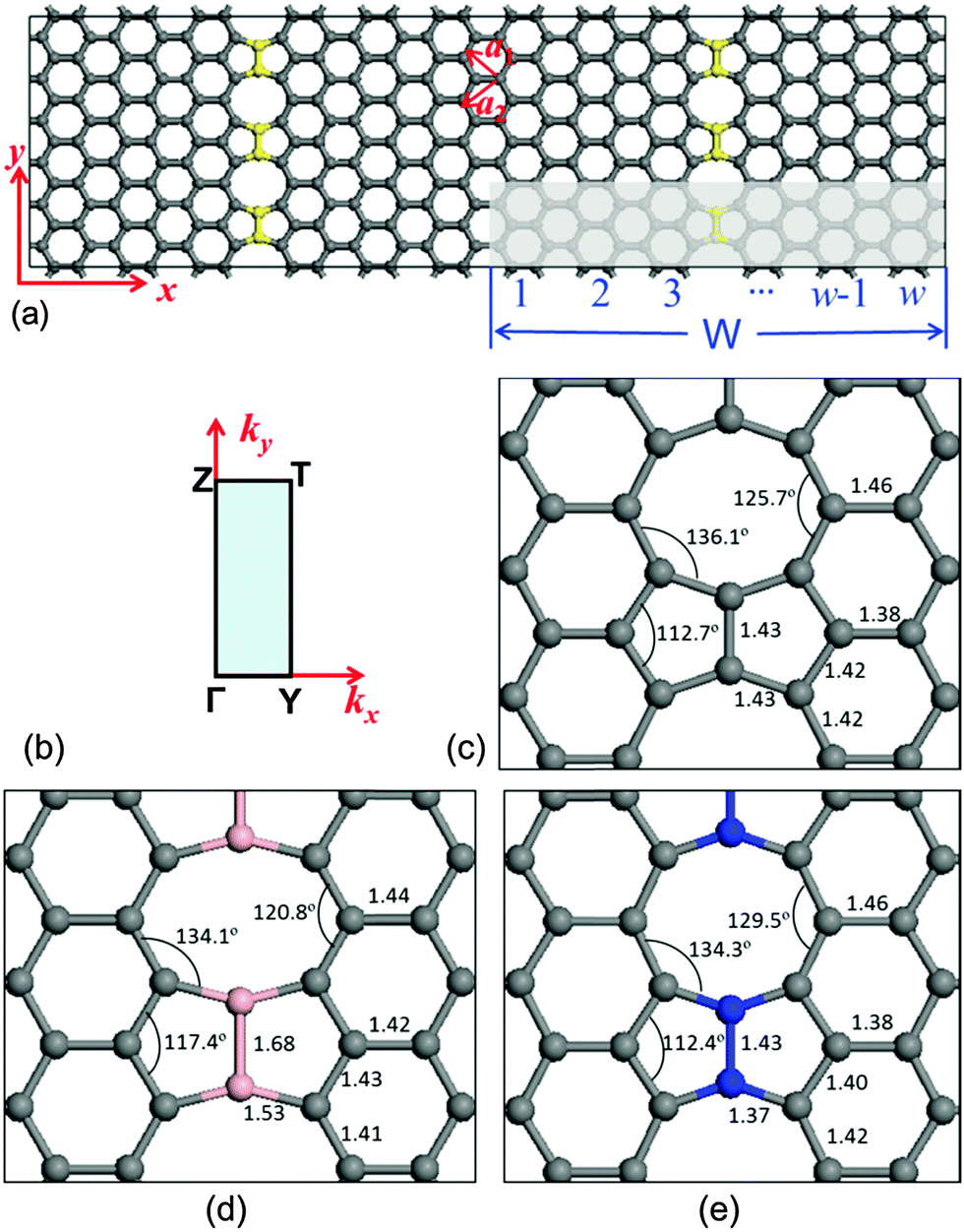 | ||
| Fig. 1 (a) Schematic illustration showing the structure of a linear C–C dimer in graphene. (b) The special high symmetry points for energy dispersion calculations in the Brillouin zone. The DFT relaxed geometries of the (c) C–C dimer, (d) B–B dimer, and (e) N–N dimer systems, including bond lengths (in Å) and bond angles. | ||
Results and discussion
Electronic properties
The electronic structures of pristine graphene and the system with C–C dimer lines embedded in graphene are shown in Fig. 2(a) and (b), respectively. They show that the linear valence and conduction bands [cyan lines in Fig. 2(a)] of graphene meet at a point of the Fermi level, which can be characterized by the Dirac cone. Therefore, the charge carriers in graphene can be considered as the massless Dirac fermions. For the system with the linear defects of C–C dimers, the bands of the graphene matrix [black solid lines in Fig. 2(b)] open the gap near the Fermi level, thus resulting in the semiconducting matrix due to the trapping effect. Note that some extra bands (pink dashed lines) introduced by the linear C–C dimers are inserted in this gap. It indicates that the defect line possesses the metallic characteristics. In addition, these extra bands at the shallow energy zone are partially flat. Therefore, the electronic states in the proximity of the Fermi level are transferred from the extended states [Fig. 2(c)] to the localized states [Fig. 2(d)]. Apparently, such localized states contain valence and conduction band edge states.25 The movement of charge carriers is confined within the quasi 1-D nanowires along the C–C dimer line.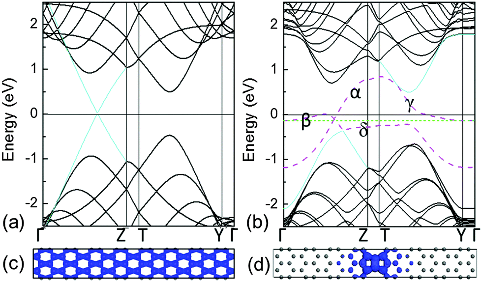 | ||
| Fig. 2 Electronic bands: (a) pristine graphene and (b) the C–C dimer system. The electronic orbitals colored in blue are: (c) pristine graphene and (d) the C–C dimer system. They are mainly induced by the bands close to the Fermi level at the low-energy zone, containing occupied and unoccupied orbitals. The solid line at 0 eV is the Fermi level of the graphene matrix exclusive of the linear defect while the dashed green line is the Fermi level of the entire system. | ||
The electronic structures show that these extra bands induced by the linear defect produce a local doping in a narrow strip. Such a self-doping phenomenon leads to the aggregation of electrons, from the graphene matrix, around the linear defect. This process leaves a number of holes in the matrix. Alike the p-doping, the Fermi level of the system labelled by the dashed green line is lowered underneath the Fermi level of the graphene matrix, as indicated by the solid black line at 0 eV in Fig. 2(b). In addition, similar to the zigzag edged graphene nanoribbons,26 the corresponding zigzag edges in this system introduce partially flat states close to the Fermi level, thus attracting the charges.12 Although the conductive 1-D nanowire has been achieved inside of 2-D graphene, its electronic band structures in the proximity of the Fermi level are not characterized by the Dirac cone. This demonstrates that its metallic character and carrier mobility are much lower than those of pristine graphene. To enhance the carrier mobility without changing the configuration of the 1-D conductive nanowire that is embedded in the 2-D graphene matrix, tailoring extra bands at the low-energy zone by doping B or N in the C–C dimers is expected to be a strategic approach.
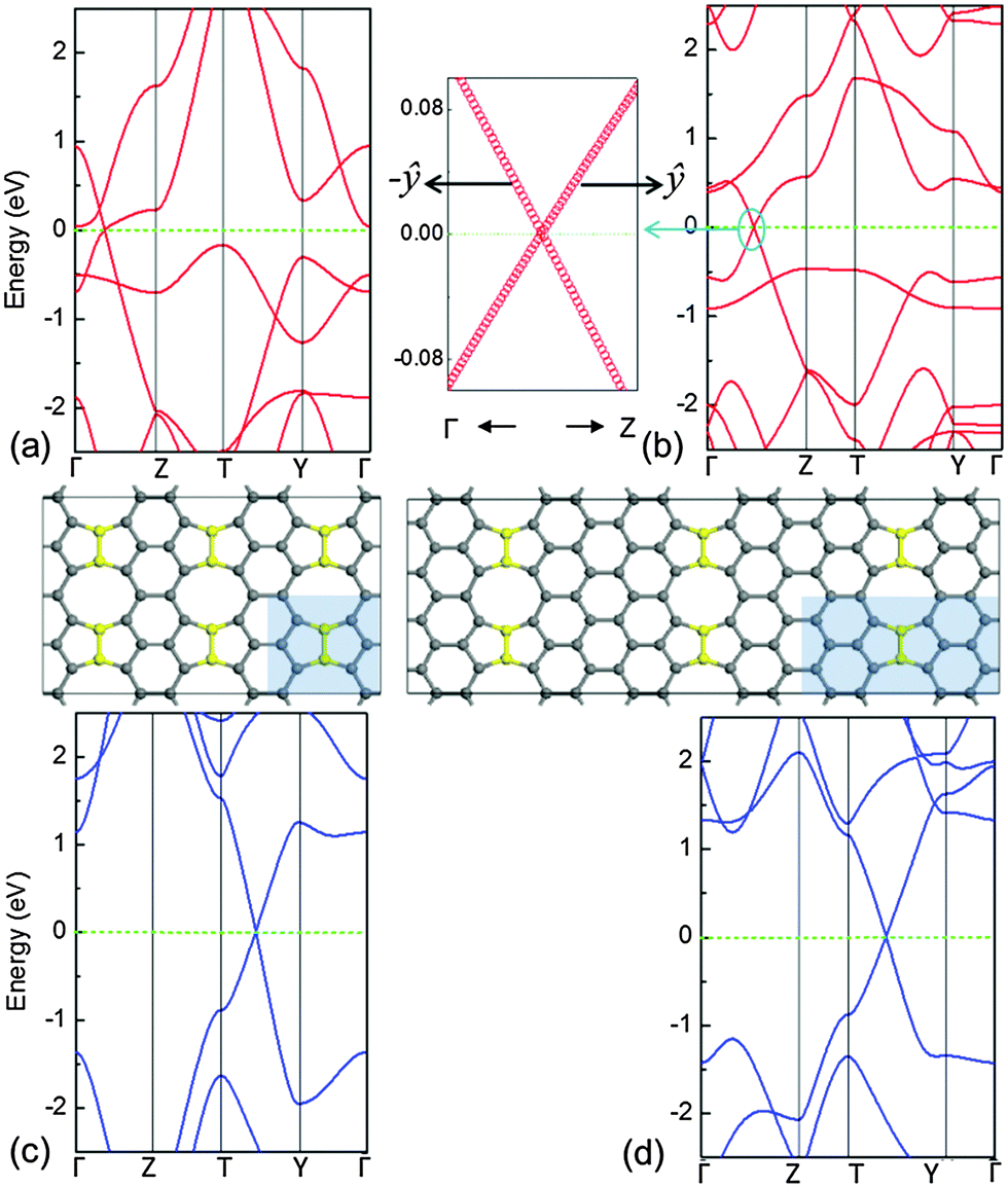
In this approach, we used B to replace a C to form the B–C dimer first and the band structure of the system with linear B–C dimers is shown in Fig. 3(a). Compared to the system with the C–C dimers, the α and δ bands in the system with a linear defect of B–C dimers are raised. In general, the doping holes push the Fermi level down, whereas the Fermi level of the entire system (graphene matrix + B–C dimer line) is very close to the one of the graphene matrix. This is because the amount of holes induced by the B substitution approximately equals that of the localized electrons around the linear defect, which are aggregated from the graphene matrix. However, there is no linear electronic band present at the Fermi level in the system with B–C dimers. The B substitutions only altered the flat electronic bands near the Fermi level in the reciprocal space partially. This gives rise to a question whether the flat bands at the Fermi level can be diminished by further increasing the B concentration. For example, double the B doping level to form the linear defects in B–B dimers to stitch the two domains of graphene. Fig. 3(b) exhibits the corresponding band dispersion of such a system. Compared with the B–C dimer system in Fig. 3(a), it is surprising to find that the β and δ bands of the system with B–B dimers are further raised to cross in a single point along the Γ–Z path at the Fermi level. Around the cross point, both the valence and conduction bands are linear and can be characterized by the Dirac cone. This cross point of the valence and conduction bands can be defined as the Dirac point (K point). In order to verify the Dirac character, the band dispersion with a large number of k-points around the K-point was calculated. The spectra displayed in the right panel of Fig. 3(b) demonstrate that the band dispersion has a linear relationship with k. In this system, there are two Dirac points appearing in its first Brillouin zone as shown in Fig. 3(c). However, due to the rectangular symmetry (pmm), only one is independent.
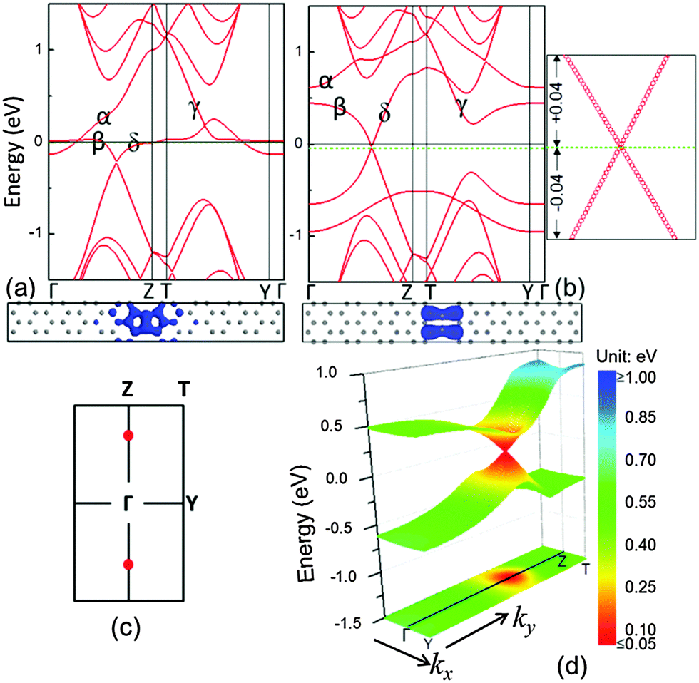 | ||
| Fig. 3 Electronic bands (top) and orbitals (bottom) of (a) B–C and (b) B–B dimer systems. The spectra in the right panel of (b) show the linear dispersion relationship in the vicinity of the Dirac point, and the unit of energy is eV. The Fermi levels of the system and the graphene matrix are indicated by green dashed and black solid lines, respectively. (c) First Brillouin zone: the red dots are the positions of the Dirac point for the B–B dimer system. (d) Energy of charge carriers in the B–B dimer system: the first band dispersion above and below the Dirac point, and projection of the first band below the Dirac point. | ||
In this case, the Fermi level of the entire system can be manipulated by controlling the concentration of B dopants. It evidences that the charge carrier is the hole in the system with B–B dimers. In addition, due to the large width of the primitive cell, the 3-D band dispersion is very narrow along the kx in the reciprocal space [Fig. 3(d)]. The energy range of the linear spectra along the ky is ∼0.9 eV and along the kx is ∼0.6 eV. The color-coded constant-energy isolines in xy projection demonstrate that the Dirac cone is nearly isotropic (the quantitative value will be reported below). In order to investigate the spatial distribution of charge carriers, the electronic orbitals at the Dirac point, containing occupied and unoccupied orbitals, are calculated and shown in the bottom panel of Fig. 3(b). It is discernable that such electronic orbitals are also confined near the dimer defect. Different from the systems with C–C and B–C dimers, the linear bands in the system with linear defect lines of B–B dimers impart a massless Dirac fermion character to the charge carriers. Therefore, when the charge carriers (holes) move in these electronic orbitals, they may transport at the speed of ∼c/300 (c is the speed of light) with a few order of magnitudes higher than the metallic-like nanowire in the C–C dimer system.
Following our finding by using B–B to substitute the C–C dimers in linear defects, it is interested to understand the physical behaviour of the substitution with the N element that has one more negative charge than the C element. Fig. 4(a) shows the band structure of the system with the linear defects, where the C–C dimers were substituted by C–N dimers. Similar to the system with B–C dimers, there is no linear electronic band present at the Fermi level, and there are some partially flat bands close to the Fermi level. Different from the B–C dimer system, the α, γ and δ bands fall in the band structures. This is because N dopants contribute more electrons to the zigzag edges than the graphene matrix. These electrons occupy the empty states in the extra bands at the low-energy zone, thus shifting the Fermi level up (green dashed line) by referring to the Fermi level of the graphene matrix (black solid line at 0 eV) in Fig. 4(a). For similar reasons, in the B–B substitution, we doubled the N doping concentration. As shown in Fig. 4(b) and (c), the system with the linear defects of N–N dimers possesses two Dirac points with an independent one at the boundary of the first Brillouin zone due to the further lowering of α and γ bands. Thus, the charge carriers in this system are attributed to massless Dirac fermions and can propagate at an effective ‘speed of light’ of ∼106 m s−1. In contrast to the B–B dimer system with the charge carriers of holes, this system with the charge carriers of electrons raised the Fermi level of the system up. In the bottom panel of Fig. 4(b), the electronic orbitals at the Dirac point, containing occupied and unoccupied orbitals, indicate that the charge carriers (electrons) in these orbitals are also confined around the dimer defect in a real space.
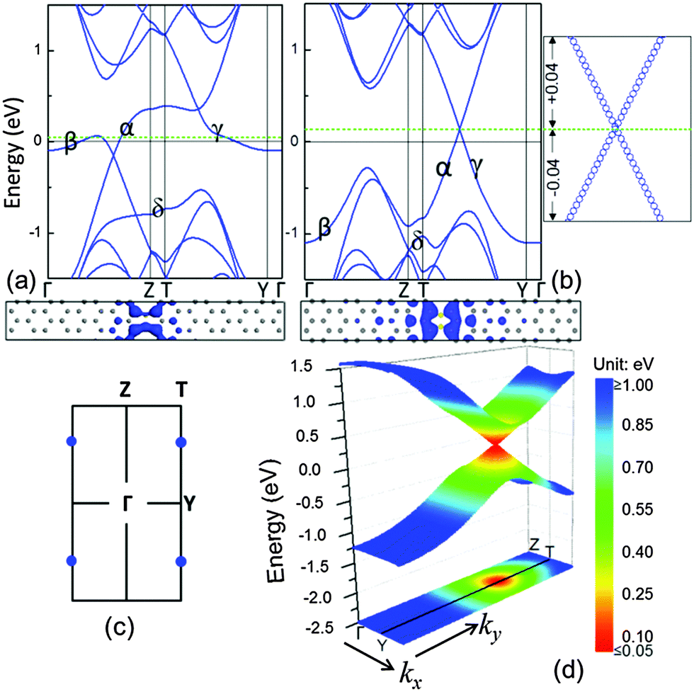 | ||
| Fig. 4 Electronic bands (top) and orbitals (bottom) of (a) C–N and (b) N–N dimer systems. The spectra in the right panel of (b) show the linear dispersion relationship in the vicinity of the Dirac point, and the unit of energy is eV. The Fermi levels of the system and the graphene matrix are indicated by green dashed and black solid lines, respectively. (c) First Brillouin zone: the blue dots are the positions of the Dirac point for the N–N dimer system. (d) The 3-D energy spectrum of the N–N dimer system: the first band dispersion above and below the Dirac point, and projection of the first band below the Dirac point. | ||
It is interesting to note that the charge carrier of the N–N dimer system is less localized than that of the B–B dimer system. The N–N dimer system has a larger energy range of the linear bands than the B–B dimer system. This is because the electrons attracted by the ionic N− dopant are much less than the holes attracted by the B+ dopant.27 The 3-D band dispersion in Fig. 4(d) exhibits that the Dirac cone is nearly isotropic for the N–N dimer system. The energy range of the linear spectrum along the ky is ∼2.0 eV and along the kx is ∼0.9 eV. In particular, the linear energy dispersion has a wider energy range compared with the B–B dimer system. Combined with the color-coded constant-energy isolines in xy projection [Fig. 3(d) and 4(d)], the slope of the Dirac cone (Fermi velocity) in the system with the linear defects of N–N dimers is larger than that in the system with B–B dimers. In addition, the linear bands gradually become flat when they are approaching the boundary of the Brillouin zone, as shown in Fig. 3(b) and 4(b); also see the ESI,† Fig. S1. Such partially flat behaviour represents the characteristics of 1-D structures, which produce the corresponding two van Hove singularities at the band extrema, as observed in the carbon nanotubes28 and graphene nanoribbons.7
Similar to the π electrons of pristine graphene to form the π bands, the extra charges introduced by the dopants also result in the bands near the Fermi level in the system with the linear defects of either B–B or N–N dimers. A portion of the extra charges produces partially flat behaviours at the deeper energy zone while the others are located at the lower energy zone to form the linear dispersion relationship. Such extra charges at the low-energy zone can be treated independently of the other charges. Therefore, around the K-point, the electronic energy is linear with respect to q = k − K that can be described as:29
| E(±) = ±ℏνFq + O[(q/k)2] | (1) |
Moreover, it is necessary to know whether or how their electronic properties varied as a function of width of the primitive cell with W. The band structures with W = 1–11 are available in Fig. S2 (ESI†). Along the kx direction, the energy range of the spectrum is width dependent, and the range decreases with an increase in W. When the periodic unit cell of the system is extremely narrow (especially for W = 1), the Dirac cone will be distorted for the B–B dimer case while the N–N dimer case still maintains a Dirac cone as shown in Fig. 5. The reason is that the weight of extra charge's distribution is large at B dopants in comparison with that at N dopants. When such strong bounding states resonate with their periodic images, they suppress and destroy the linear dispersion. Additionally, for the B–B dimer case with W = 1, there is another conduction band touching the Fermi level at the Γ point. For the B–B dimer case with W = 2, the band shows a finite curvature in the ŷ direction in Fig. 5(b). However, following the notation of ref. 10, if the conduction and valence bands meet in a single point at or very close to the Fermi level with a zero curvature along at least one direction, a double cone-like feature will be observed, denoted the Dirac cone. The values of νF along the indicated directions with a width of W are listed in Table 1. It is displayed that the νF of narrow structures depends on the direction of the Dirac point in the k space, thus its cone will be anisotropic. The νF of the N–N dimer case is larger than that of the B–B dimer case due to a different ability of bounding extra charges. It is very interesting to note that when the width of W is very narrow, for example W = 1 or 2 as in Fig. 5, also see the 3-D energy spectrum in a reciprocal space and its corresponding electronic orbitals in a real space in Fig. S3 (ESI†), the new 2-D feature appears in which some chains of the C six-membered ring are bonded by B–B or N–N dimers.
 | ||
| Fig. 5 Band structures of B–B/N–N dimer cases with W = 1 (a) and (c) and W = 2 (b) and (d). The spectrum in the left (b) shows the magnified image of the band dispersion of the cycled area around the band intersection at the Fermi level in the right panel for the B–B dimer case with W = 2, where one ŷ branch is slightly curved. The Fermi level of the system is set to 0 eV. Inset: schematic illustration showing the structure of B–B/N–N dimer cases with W = 1 (left) and W = 2 (right). | ||
| W | 1 | 2 | 3 | 4 | 5 | 6 | 7 | 8 | 9 | 10 | 11 | |
|---|---|---|---|---|---|---|---|---|---|---|---|---|
| B | ŷ | — | — | 0.66 | 0.67 | 0.69 | 0.69 | 0.69 | 0.70 | 0.71 | 0.70 | 0.71 |
| −ŷ | — | 0.75 | 0.71 | 0.70 | 0.69 | 0.69 | 0.69 | 0.70 | 0.69 | 0.69 | 0.69 | |
| N | ŷ | 1.00 | 0.88 | 0.84 | 0.83 | 0.82 | 0.82 | 0.82 | 0.82 | 0.81 | 0.82 | 0.83 |
| −ŷ | 0.63 | 0.70 | 0.75 | 0.77 | 0.78 | 0.79 | 0.80 | 0.81 | 0.81 | 0.81 | 0.81 | |
Stability
The geometric structures of B–B/N–N dimer systems with W = 8 are shown in Fig. 1(d) and (e). In comparison with the C–C dimer system [Fig. 1(c)], the B–B dimer system stretches along the width while the N–N dimer system contracts along the width. The stability of the as-designed dimer lines embedded in graphene is essential for the applications of nanoelectronics. To address this issue, we firstly calculate the cohesive energy Ecoh per atom of the as-designed systems for evaluating the structural stability using the following equation: | (2) |
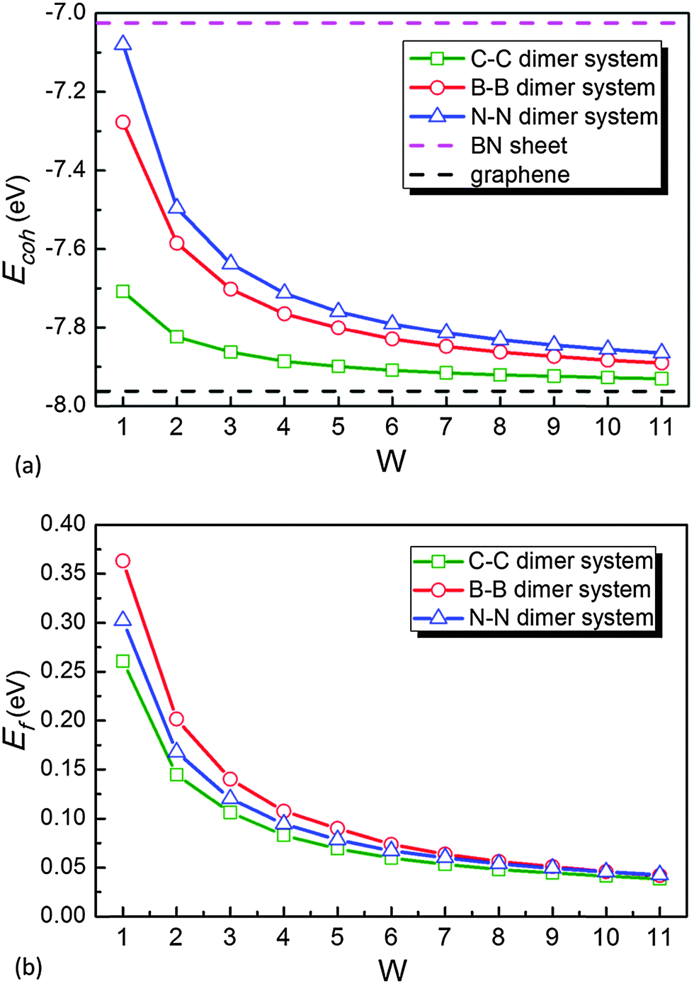 | ||
| Fig. 6 (a) Calculated cohesive energies (Ecoh) and (b) formation energies (Ef) per atom of the periodically repeated arrays of linear C–C, B–B or N–N dimers in graphene as a function of primitive cell width (W). | ||
Further consideration should be made for the thermodynamic stability of the as-designed systems. In this case, the formation energy Ef per atom can be calculated as
 | (3) |
To study their stability at room temperature, molecular dynamics simulations for B–B/N–N dimer systems with W = 1, 8 have also been performed. The graphene embedded with defect dimer lines is basically stable, and have a slight fluctuation after 3 ps molecular dynamics simulations (see ESI,† Fig. S3). Therefore, it is possible that the C–C dimer in graphene would be replaced by a B–B or N–N dimer.
Conclusions
We proposed a methodology to engineer a 1-D electron tunnel by manipulating the 2-D structure with the B–B or N–N dimer lines in the graphene matrix. It is found that the Dirac cone appears in the bands introduced by the B–B or N–N dimers at the low-energy zone. It results in the transport velocities of the charge carriers to be ∼106 m s−1, an effective “speed of light”, which are comparable with the pristine graphene. Such systems suggest that heteroatoms in graphene can indeed contribute to the Dirac cone. However, different from the 2-D charge carriers in pristine graphene, the charge carriers introduced by B or N dopants are confined in a very thin nanowire along the B–B or N–N dimer lines in a real space. Therefore, the B–B or N–N dimer lines periodically distributed in graphene can act as a quasi-high conductive nanowire while the graphene matrix possesses the characteristics of a semi-conductor. Such a structure with the 1-D conductive dimer lines and a semiconductor matrix is similar to the current basic structure of the integrated circuit, whose conductive metal nanowires are embedded in a semiconducting Si-based material matrix. In addition, owing to the ultrahigh carrier mobility and ultra-thin width (less than 0.8 nm) of the B–B or N–N dimer line, the proposed structure would be a promising candidate for the high performance ultra-large-scale integrated circuit. In particular, the type of carriers can be manipulated by controlling the dopants, such as B or N, to meet the specific requirements of the applications.Acknowledgements
The authors would like to thank the financial support from the National Natural Science Foundation of China (Grant No. 51372095), the Fundamental Research Funds of Jilin University (Grant No. 201103021), Program for Changjiang Scholars and Innovative Research Team in University (PCSIRT), and the “211” and “985” projects of Jilin University, as well as Australian Research Council FT100100956 and DP140104373. Quanguo Jiang and Quan Li are acknowledged for their help in the discussion and calculation.Notes and references
- J. D. Meindl, J. Vac. Sci. Technol., B: Microelectron. Nanometer Struct. – Process., Meas., Phenom., 1996, 14, 192 CrossRef CAS.
- K. S. Novoselov, A. K. Geim, S. V. Morozov, D. Jiang, Y. Zhang, S. V. Dubonos, I. V. Grigorieva and A. A. Firsov, Science, 2004, 306, 666 CrossRef CAS PubMed.
- K. S. Novoselov, A. K. Geim, S. V. Morozov, D. Jiang, M. I. Katsnelson, I. V. Grigorieva, S. V. Dubonos and A. A. Firsov, Nature, 2005, 438, 197 CrossRef CAS PubMed.
- Y. B. Zhang, Y. W. Tan, H. L. Stormer and P. Kim, Nature, 2005, 438, 201 CrossRef CAS PubMed.
- J. S. Davies, The Physics of Low-Dimensional Semiconductors, Cambridge University Press, New York, 1998 Search PubMed.
- J. S. Bunch, Y. Yaish, M. Brink, K. Bolotin and P. L. McEuen, Nano Lett., 2005, 5, 287 CrossRef CAS PubMed.
- A. H. Castro Neto, F. Guinea, N. M. R. Peres, K. S. Novoselov and A. K. Geim, Rev. Mod. Phys., 2009, 81, 109 CrossRef CAS.
- C.-H. Park, L. Yang, Y.-W. Son, M. L. Choen and S. G. Louie, Nat. Phys., 2008, 4, 213 CrossRef CAS.
- J. Lahiri, Y. Lin, P. Bozkurt, I. I. Oleynik and M. Batzill, Nat. Nanotechnol., 2010, 5, 326 CrossRef CAS PubMed.
- (a) D. Malko, C. Neiss, F. Viñes and A. Görling, Phys. Rev. Lett., 2012, 108, 086804 CrossRef; (b) D. Malko, C. Neiss and A. Görling, Phys. Rev. B: Condens. Matter Mater. Phys., 2012, 86, 045443 CrossRef.
- L. C. Xu, R. Z. Wang, M. S. Miao, X. L. Wei, Y. P. Chen, H. Yan, W. M. Lau, L. M. Liu and Y. M. Ma, Nanoscale, 2014, 6, 1113 RSC.
- S. S. Yu and W. T. Zheng, Nanoscale, 2010, 2, 1069 RSC.
- D. Wei, Y. Liu, Y. Wang, H. Zhang, L. Huang and G. Yu, Nano Lett., 2009, 9, 1752 CrossRef CAS PubMed.
- H. B. Wang, T. Maiyalagan and X. Wang, ACS Catal., 2012, 2, 781 CrossRef CAS.
- H. Wang, Y. Zhou, D. Wu, L. Liao, S. Zhao, H. Peng and Z. F. Liu, Small, 2013, 9, 1316 CrossRef CAS PubMed.
- Y. C. Lin, C. Y. Lin and P. W. Chiu, Appl. Phys. Lett., 2010, 96, 133110 CrossRef PubMed.
- Y. Wang, Y. Shao, D. W. Matson, J. Li and Y. Lin, ACS Nano, 2010, 4, 1790 CrossRef CAS PubMed.
- Y. Li, J. C. Ren, R. Q. Zhang, Z. Lin and M. A. Van Hove, J. Mater. Chem., 2012, 22, 21167 RSC.
- S. S. Yu, X. M. Zhang, L. Qiao, Z. M. Ao, Q. F. Geng, S. Li and W. T. Zheng, RSC Adv., 2014, 4, 1503 RSC.
- (a) B. Delley, J. Chem. Phys., 1990, 92, 508 CrossRef CAS PubMed; (b) B. Delley, J. Chem. Phys., 2000, 113, 7756 CrossRef CAS PubMed.
- J. P. Perdew, Phys. Rev. Lett., 1996, 77, 3865 CrossRef CAS.
- S. J. Clark, M. D. Segall, C. J. Pickard, P. J. Hasnip, M. J. Probert, K. Refson and M. C. Payne, Z. Kristallogr., 2005, 220, 567 CrossRef CAS.
- G. Kresse and J. Furthmuller, Phys. Rev. B: Condens. Matter Mater. Phys., 1996, 54, 11169 CrossRef CAS.
- Y. D. Ma, Y. Dai and B. B. Huang, J. Phys. Chem. Lett., 2013, 4, 2471 CrossRef CAS.
- D. J. Appelhans, L. D. Carr and M. T. Lusk, New J. Phys., 2010, 12, 125006 CrossRef.
- C. Q. Sun, S. Y. Fu and Y. G. Nie, J. Phys. Chem. C, 2008, 112, 18927 CAS.
- C. L. Muhich, J. Y. Westcott, T. C. Morris, A. W. Weimer and C. B. Musgrave, J. Phys. Chem. C, 2013, 117, 10523 CAS.
- J.-C. Charlier, X. Blase and S. Roche, Rev. Mod. Phys., 2007, 79, 677 CrossRef CAS.
- J.-C. Charlier, P. C. Eklund, J. Zhu and A. C. Ferrari, Top. Appl. Phys., 2008, 111, 673 CrossRef PubMed.
- S. Cahangirov, M. Topsakal, E. Aktürk, H. Saghin and S. Ciraci, Phys. Rev. Lett., 2009, 102, 236804 CrossRef CAS.
- A. K. Manna and S. K. Pati, J. Phys. Chem. C, 2011, 115, 10842 CAS.
- D. Kitchen, A. Richardella, J. M. Tang, M. E. Flatte and A. Yazdani, Nature, 2006, 442, 436 CrossRef CAS PubMed.
Footnote |
| † Electronic supplementary information (ESI) available: The wide energy bands of B–B/N–N dimer systems with and without relaxing cell lattices. The electronic bands with W = 1–11 using GGA. The 3-D energy spectrum and its corresponding electronic orbitals with W = 2. See DOI: 10.1039/c4cp05193a |
| This journal is © the Owner Societies 2015 |