
 Open Access Article
 This Open Access Article is licensed under a
 Creative Commons Attribution 3.0 Unported Licence
Surface- and tip-enhanced resonant Raman scattering from CdSe nanocrystals
E.
Sheremet†
*a,
A. G.
Milekhin
*bc,
R. D.
Rodriguez‡
a,
T.
Weiss
d,
M.
Nesterov
d,
E. E.
Rodyakina
bc,
O. D.
Gordan
a,
L. L.
Sveshnikova
b,
T. A.
Duda
b,
V. A.
Gridchin
e,
V. M.
Dzhagan
a,
M.
Hietschold
f and
D. R. T.
Zahn‡
a
aSemiconductor Physics, Technische Universität Chemnitz, D-09107 Chemnitz, Germany. E-mail: evgeniya.sheremet@physik.tu-chemnitz.de
bA.V. Rzhanov Institute of Semiconductor Physics, pr. Lavrentieva, 13, Novosibirsk 630090, Russia. E-mail: amilekhin@hotmail.com
cNovosibirsk State University, Pirogov str. 2, Novosibirsk 630090, Russia
d4th Physics Institute and Research Center SCoPE, University of Stuttgart, D-70550 Stuttgart, Germany
eNovosibirsk State Technical University, K. Marx av.20, Novosibirsk 630073, Russia
fSolid Surfaces Analysis Group, Technische Universität Chemnitz, D-09107 Chemnitz, Germany
First published on 22nd December 2014
Abstract
Surface- and tip-enhanced resonant Raman scattering (resonant SERS and TERS) by optical phonons in a monolayer of CdSe quantum dots (QDs) is demonstrated. The SERS enhancement was achieved by employing plasmonically active substrates consisting of gold arrays with varying nanocluster diameters prepared by electron-beam lithography. The magnitude of the SERS enhancement depends on the localized surface plasmon resonance (LSPR) energy, which is determined by the structural parameters. The LSPR positions as a function of nanocluster diameter were experimentally determined from spectroscopic micro-ellipsometry, and compared to numerical simulations showing good qualitative agreement. The monolayer of CdSe QDs was deposited by the Langmuir–Blodgett-based technique on the SERS substrates. By tuning the excitation energy close to the band gap of the CdSe QDs and to the LSPR energy, resonant SERS by longitudinal optical (LO) phonons of CdSe QDs was realized. A SERS enhancement factor of 2 × 10³ was achieved. This allowed the detection of higher order LO modes of CdSe QDs, evidencing the high crystalline quality of QDs. The dependence of LO phonon mode intensity on the size of Au nanoclusters reveals a resonant character, suggesting that the electromagnetic mechanism of the SERS enhancement is dominant. Finally, the resonant TERS spectrum from CdSe QDs was obtained using electrochemically etched gold tips providing an enhancement on the order of 104. This is an important step towards the detection of the phonon spectrum from a single QD.
Introduction
Quantum dots (QDs) attracted intense research interest due to their potential for electronic and optoelectronic applications.1 Among them, CdSe QDs are promising for numerous applications in photodetectors, field-effect transistors, solar cells, light-emitting diodes.2–4 The information about the phonon spectrum of QDs is important for practical applications, since the phonons determine the channels for charge carrier relaxation in QD based devices.5–7 Phonon spectra from an ensemble of QDs can be obtained by Raman spectroscopy (RS), which provides information on QD size,8 shape,9 as well as strain relaxation10 and atomic intermixing.11,12 Since the properties of QDs are strongly sensitive to the QD size and environment, analyzing the phonon spectrum of a single QD would give valuable insight into the individual QD properties. However, the intensity of the Raman signal from a single QD is often too low to be detected, and therefore methods to amplify it are required.One of the well-established methods to enhance the Raman signal is resonant Raman spectroscopy (RRS), which is achieved by choosing the excitation wavelength close to (or at) the band gap energy of the QD system studied. However, enhancement provided by RRS reaches 103, and this is not sufficient for the detection of very small amounts of material, such as a single QD.
Surface- and tip-enhanced Raman spectroscopies (SERS and TERS) are two actively developing approaches, which drastically improve the sensitivity and spatial resolution of RS. They are based on the enhancement of the electromagnetic field by localized surface plasmons (LSPs) of metallic nanoclusters to drastically increase the intensity of relatively weak Raman scattering by up to 107 times.13,14 In the case of organic molecules, single-molecule sensitivity was achieved by both SERS15,16 and TERS.17–19 These methods were also employed to detect the signal from low amounts of inorganic materials, such as CdS, CdSe, GaN, CuxS, and ZnO.20–24 Recently, resonant SERS was successfully employed to analyze the anisotropy of the phonon spectrum of a single CdSe nanoplatelet.25 The scattering volume of a single QD is 30 times smaller than that of a nanoplatelet, which makes the task of detecting a single QD challenging.
TERS is the ultimate case of SERS, it breaks the diffraction limit of light and thus drastically improves the spatial resolution of the conventional RS. This is accomplished using the apex of a tip as a single plasmonic scatterer, and moving it in a controlled manner with respect to the sample. The power of TERS to improve the spatial resolution was demonstrated on single nanowires and crystallites26–28 with a resolution comparable to that of AFM imaging. Raman and photoluminescence spectra of CdSe nanowires were investigated as well, achieving optical resolution below AFM resolution in the same experiment due to the square-law field dependence of both the excitation and the emission rates.29,30 The improved spatial resolution of TERS also allowed mapping of stress and composition within a single quantum dot.31
The enhancement of the Raman signal can be maximized by simultaneously employing RRS and SERS (or TERS). This requires matching the excitation energy (wavelength) to the band gap of QDs, as well as to the localized surface plasmon resonance (LSPR) energy of a plasmonic structure. The LSPR position can be tuned by changing the size, the shape, and the distance between the plasmonic nanostructures.32 Electron beam lithography provides unique control of all those parameters allowing optimization of the SERS signal.33,34
In this paper, both resonant SERS and TERS were employed in order to detect a monolayer of CdSe QDs deposited by the Langmuir–Blodgett-based technique.
Results and discussion
SERS substrates are prepared on Si substrates, and consist of gold nanocluster arrays with the period of 150, while the nanocluster diameters were systematically varied from 70 nm to 140 nm. It was shown that the arrays of gold nanoclusters serve as effective SERS substrates providing SERS by organic and biological substances,35–37 including our previous studies using the CoPc dye as a Raman probe.38,39 In our case the CdSe QDs of 5.2 nm size deposited by the Langmuir–Blodgett-based technique play the role of the Raman probe. The deposition procedure is described in the experimental section. The QDs form a homogeneous coverage on the Si substrate as well as on the gold nanocluster arrays, as confirmed by SEM measurements (Fig. 1). | ||
| Fig. 1 SEM image of an edge of the nanostructured gold array (left side, white areas are the gold nanoclusters) demonstrating homogeneous coverage of both nanostructure and a Si substrate with a monolayer of CdSe QDs. Inset shows the high resolution SEM image of the CdSe QD monolayer on the Si substrate. | ||
LSPR position
The LSPR positions were characterized by spectroscopic micro-ellipsometry. The LSPR position was determined as the maximum of the extinction coefficient spectrum extracted from ellipsometry measurements. The dependence of the LSPR position on the gold nanocluster diameter is shown in Fig. 2. The data show an increase of the LSPR position with an increase in the gold nanocluster diameter. These results are in agreement with the well-established behaviour of the LSPR position.32 | ||
| Fig. 2 LSPR position determined from ellipsometry measurements (squares) and simulations (solid line) depending on gold nanocluster size for the 150 nm array period. The crosses indicate the wavelengths, for which maxima of the SERS enhancement were observed (see section surface-enhanced Raman spectroscopy of CdSe QDs). | ||
To better understand the resonant behaviour of the structure, the extinction coefficients and LSPR positions were numerically modeled using the Fourier modal method with adaptive spatial resolution and matched coordinates.40,41 It is important to note that the LSPR position strongly depends on the dielectric function of the gold nanocluster environment. Direct experimental determination of the dielectric function around the gold nanoclusters is challenging, since the optical response is dominated by the signal of the gold nanoclusters. Therefore, the optical response of the silicon substrate covered by a monolayer of CdSe QDs was measured. The dielectric function of the CdSe QD monolayer can be approximated for this thickness range by a Cauchy dispersion. As a result, in the spectral region of interest, the optical response of the system is equivalent to a 11 nm SiO2 layer on the Si substrate. The calculated LSPR positions of the gold nanoclusters on the Si substrate with 11 nm SiO2 thickness give good agreement with the experiment (Fig. 2), showing the red shift of the LSPR position with an increase in the nanocluster diameter. When the distance between the neighbouring nanoclusters drops below 20 nm, the near-field coupling effect leads to further red shift of the LSPR position.
Surface-enhanced Raman spectroscopy of CdSe QDs
The Raman and SERS spectra of the CdSe monolayer are shown in Fig. 3. In this case, Raman spectra are resonant, since the excitation wavelength (632.8 nm) approaches the specified emission maximum (610 nm) determined by the energy of interband transition in CdSe QDs. The Raman spectra of the CdSe QDs deposited on a Si substrate show only clear bands of the Si substrate (second-order transverse acoustic (2TA) phonon mode at 300 cm−1 and LO mode at 520 cm−1) and no detectable signal of the CdSe QDs. The resonant SERS allows the detection of an intense first order Raman scattering by LO phonons of the CdSe QDs at 207 cm−1, which is in agreement with previously reported values,42–44 as well as of higher order modes. For the specified CdSe size of 5.2 nm no strong phonon confinement effect and therefore no confinement induced shift of LO phonon mode in CdSe QDs are expected, as shown experimentally44 and theoretically.45 The observation of higher order features in the Raman spectrum reveals a remarkable crystalline quality of the QDs. The first order feature also exhibits a broad background, which can be attributed either to the enhanced signal from amorphous Se on the QD surface,46 or to scattering from the SERS substrate. The effective SERS enhancement factor (EF) was estimated as a ratio of the LO signal intensity of CdSe QDs on the SERS substrate to the noise level on the Si substrate, since the CdSe signal was not detectable on the Si substrate. The resulting EF is approximately 2 × 10³. | ||
| Fig. 3 Raman (black curve) and SERS (red curve) spectra of CdSe QDs measured with a 632.8 nm laser line for a nanocluster diameter of 80 nm. | ||
The normalized dependence of the LO phonon mode intensity on the Au nanocluster diameter obtained using different excitation wavelengths is shown in Fig. 4. The curves show a clear resonant behaviour, with the maximum of the Raman signal shifting to larger nanocluster sizes when increasing the excitation wavelength. The nanocluster sizes and wavelengths, for which the maximum SERS enhancement was observed, were compared to the LSPR positions measured with micro-ellipsometry (crosses in Fig. 2). Clearly, for a given nanocluster size, the maximum enhancement is observed when the excitation wavelength matches the measured maximum LSPR position. This implies that the resulting SERS enhancement is dominated by the electromagnetic enhancement, rather than the intrinsic resonance of CdSe NCs or chemical enhancement.
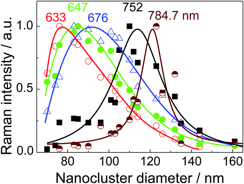 | ||
| Fig. 4 Normalized dependence of the Raman intensity of the CdSe LO phonon on the gold nanocluster diameter for different wavelengths (indicated in the figure). | ||
TERS measurements
Detection of fewer QDs as compared to SERS measurements was achieved in a TERS experiment on the CdSe QD monolayer deposited on the SERS structure with 88 nm nanocluster diameter, which is close to the resonance observed for the 632.8 nm excitation line according to Fig. 4. Note that the shift of the resonance can be caused by the metallic tip when it approaches an Au nanocluster. The comparison of SERS and TERS spectra is shown in Fig. 5. In the TERS experiment, the area of the laser spot is approximately 1.5 × 2.5 μm2, giving rise to the so-called far-field signal (tip up in Fig. 5b). When the electrochemically etched gold tip was brought into contact with the QDs, the Raman signal from the QDs located directly under the tip apex was enhanced (tip down in Fig. 5b). It was possible to achieve a 100% increase of the CdSe LO mode intensity at 207 cm−1. Similar to SERS spectra, the increased background at low frequency can be attributed to enhancement of the signal from amorphous Se on the QD surface, and partially to elastic scattering from the tip.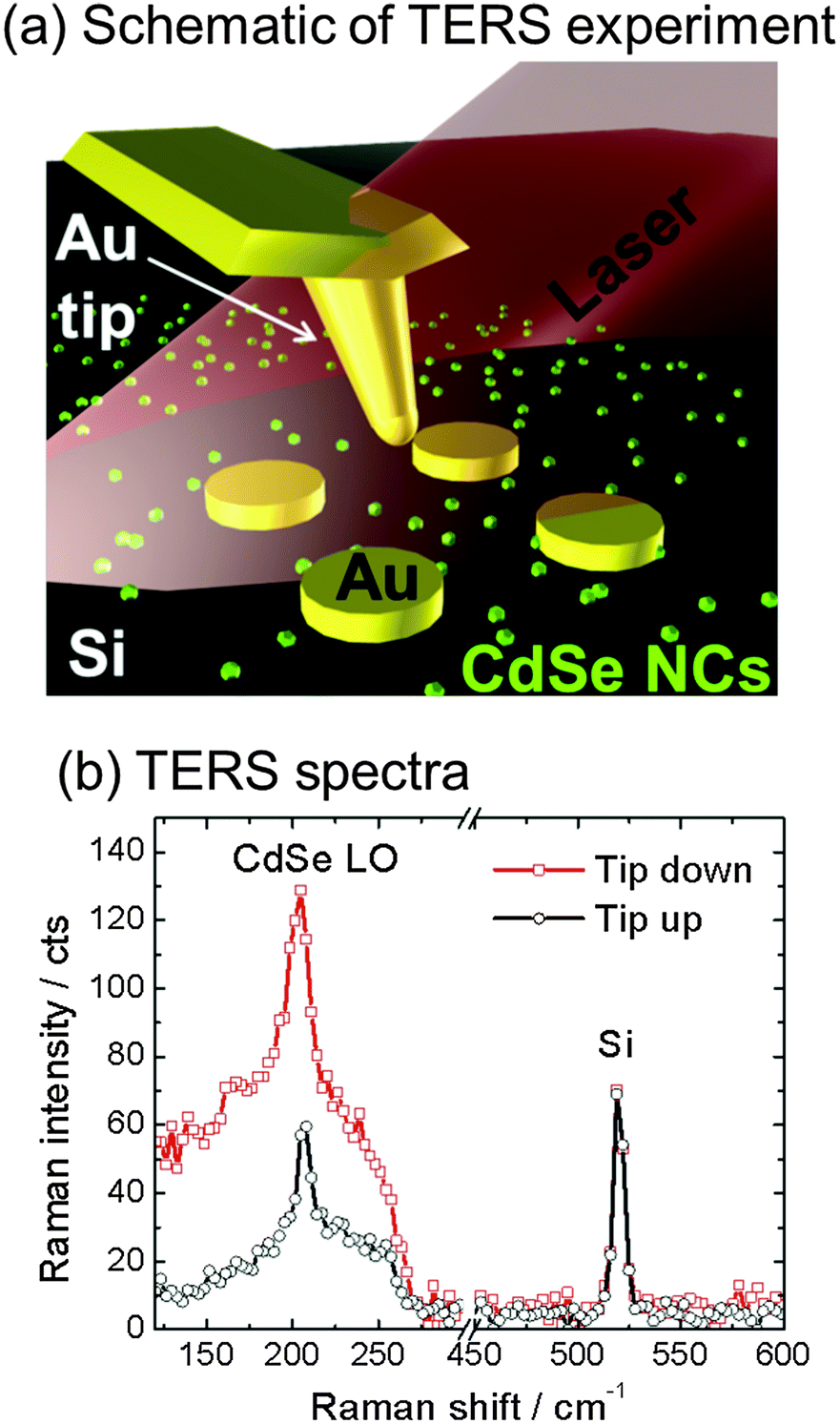 | ||
| Fig. 5 TERS of the CdSe monolayer on the SERS substrate. (a) Schematic of the experiment (not in scale). (b) Raman spectra of tip in contact (tip down) and tip away from the sample (tip up). | ||
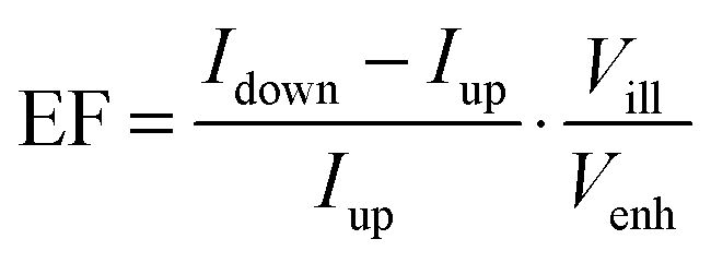
The latter could lead to an increase of the Raman signal not related to the near-field enhancement.47,48 However, since the intensity of the Si peak remains the same, such a signal increase can be excluded,39 and the TERS EF can be estimated using the formula:
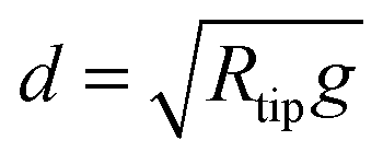
The area of the illuminated volume is defined by the laser spot size. Then the enhanced area diameter was estimated to be49
Solving the problem of packing smaller circles in a larger circle, we can then expect seven CdSe QDs in the enhanced area.
Experimental
SERS substrate preparation
The 10 × 10 μm2 gold nanocluster arrays with a period of 150 nm to be used as SERS substrates were prepared by a direct-write electron beam lithography process. The electron resist (polymethyl methacrylate 950 K) deposited on an Si(100) substrate was structured with an electron beam (20 kV, Raith-150, Germany), and the patterned resist was covered with a 5 nm thick film of Ti and a 40 nm thick film of Au. Finally, the remaining resist was removed by a lift-off process in dimethylformamide to obtain isolated gold nanoclusters with diameters from 70 nm to 140 nm.Langmuir–Blodgett-based deposition
The deposition of CdSe NCs was performed using the Langmuir–Blodgett-based (LB-based) technique. Pre-synthesized CdSe NCs of 5.2 nm diameter (Lumidot™ 610) were mixed with behenic acid and deposited using the LB-based approach. Note that it is not clear where exactly NCs are incorporated in organics. After 20 cycles of LB-based deposition, the sample was annealed at 200 °C in order to remove the organic matrix, and a monolayer of CdSe NCs was formed. The removal of organic layer was confirmed by infrared (IR) and energy-dispersive X-ray (EDX) spectroscopies.Micro-ellipsometry
The SERS substrates covered by a monolayer of CdSe QDs were investigated by nulling micro-ellipsometry to determine the LSP resonance position using a Spectroscopic Imaging Ellipsometer (EP3-SE, Accurion GmbH) with the spectral range of 365–1000 nm (3.4–1.24 eV).The measured sample was modelled as a multi-layer system, taking into account the optical properties of the substrate. Here a Maxwell–Garnet effective medium approximation (MG-EMA) was used. The dielectric functions of silicon, silicon dioxide and gold were taken from the commercially available Woollam WVASE32 3.6 database. The substrate was modelled as a silicon substrate with a silicon oxide thickness of 11 nm. The dielectric function obtained for the MG-EMA layer is strongly dominated by the metallic nanostructures on top of the substrate, matching the effective dielectric function of the system. In turn this makes the determination of the LSPR peak possible even by directly recalculating measured effective optical constants to the extinction coefficient.
Simulations
The extinction coefficients and LSP positions were numerically modeled using the Fourier modal method with adaptive spatial resolution and matched coordinates.40,41 This approach is very efficient for calculating layered periodic systems fabricated by electron beam lithography. The model volume consists of a semi-infinite silicon substrate (constant refractive index of n = 3.68), a 11 nm SiO2 layer (n = 1.46) and a 40 nm high gold disk. The analytical model of the dielectric function for gold was taken from the work of Etchegoin et al.50Micro-Raman measurements
Raman experiments were carried out using Jobin Yvon Dilor XY800, Horiba T64000, and Labram HR800 spectrometers equipped with optical microscopes (the laser beam was focused to a spot with a size of approximately 1 μm2 using 100× objective with N.A. 0.9) in a backscattering geometry at room temperature. The 632.8 nm (1.96 eV) line of a HeNe laser (Siemens), and several lines of a Kr+ laser (Coherent) were used as excitation sources. A laser power below 1 mW was used in the experiment to avoid possible effects of local heating. For the SERS spectra (on Au nanocluster arrays) 10 s acquisition time, 15 accumulations were performed; each Raman spectrum (on Si) was acquired for 30 s, 60 accumulations, and the Raman intensity was divided by a factor of 3 in order to compare the intensities.TERS measurements
For the TERS experiments, a Raman spectrometer (LabRam HR800) was coupled to an Agilent 5420 (Agilent, USA) atomic force microscope (AFM). A custom-made optical extension delivered the laser light to the AFM tip at an angle of 70° with respect to the sample normal axis. A 50× magnification long-working-distance objective lens with N.A.0.42 (Mitutoyo, Japan) was used both to focus the laser light onto the tip in the vicinity of the sample surface and to collect the scattered light. The 632.8 nm laser line with a laser power of 0.4 mW on the sample was used. The mirror and objective lens of the optical extension unit were driven by piezoelectric motors to improve the system stability when aligning the laser on the tip. A fully metallic gold tip cantilever was used in contact mode in the AFM for the TERS measurements. The cantilever preparation procedure is described elsewhere.51 The tip apex was sharpened by electrochemical etching. The TERS spectra were recorded with tip down (in contact with the surface) and tip up (tip retracted by 1 μm) on the gold nanocluster array with a 150 nm period. The gold nanocluster diameter was 88 nm. The TERS spectra were accumulated for 5 s.Conclusions
The LSPR positions of gold nanocluster arrays fabricated by electron beam lithography were measured using spectroscopic micro-ellipsometry and compared to values calculated using the Fourier modal method. Both the experimental and the computational approach show that the LSPR position red-shifts with an increase in the nanocluster diameter. Using these SERS substrates, an enhancement factor as high as 2 × 10³ for the Raman scattering by the CdSe LO phonon mode was demonstrated for a CdSe QD monolayer. SERS allowed the detection of higher order phonon modes for CdSe QDs, demonstrating their remarkable crystalline quality. The dependence of SERS enhancement on the nanocluster diameter for different excitation wavelengths reveals a resonance behaviour suggesting that the electromagnetic enhancement mechanism dominates. Finally, TERS results obtained from the CdSe QD monolayer on the SERS substrate allowed acquiring the spectrum of fewer QDs as compared to micro-Raman measurements with an additional enhancement on the order of 104. This opens up a prospective for studying phonon spectra of QD arrays of a low areal density.Acknowledgements
Authors thank DFG project ZA146/22-1, DFG Research Unit 1713 SMINT, Russian Science Foundation (project 14-12-01037), and Cluster of Excellence for Advanced Electronics Dresden (cfaed) for financial support. AM thanks DAAD for providing a scholarship. This work was performed in the context of the European COST Action MP1302 Nanospectroscopy. M. N. acknowledges financial support through an Alexander von Humboldt research fellowship.Notes and references
- T. Trindade, P. O'Brien and N. L. Pickett, Chem. Mater., 2001, 13, 3843–3858 CrossRef CAS.
- L. J. Zhao, L. F. Hu and X. S. Fang, Adv. Funct. Mater., 2012, 22, 1551–1566 CrossRef CAS.
- V. I. Klimov, A. A. Mikhailovsky, S. Xu, A. Malko, J. A. Hollingsworth, C. A. Leatherdale, H. J. Eisler and M. G. Bawendi, Science, 2000, 290, 314–317 CrossRef CAS.
- R. C. Somers, M. G. Bawendi and D. G. Nocera, Chem. Soc. Rev., 2007, 36, 579–591 RSC.
- A. V. Uskov, A. P. Jauho, B. Tromborg, J. Mork and R. Lang, Phys. Rev. Lett., 2000, 85, 1516–1519 CrossRef CAS.
- A. J. Nozik, Annu. Rev. Phys. Chem., 2001, 52, 193–231 CrossRef CAS PubMed.
- V. I. Klimov, D. W. McBranch, C. A. Leatherdale and M. G. Bawendi, Phys. Rev. B: Condens. Matter Mater. Phys., 1999, 60, 13740–13749 CrossRef CAS.
- D. A. Tenne, A. K. Bakarov, A. I. Toropov and D. R. T. Zahn, Phys. E, 2002, 13, 199–202 CrossRef CAS.
- D. A. Tenne, A. K. Bakarov, A. I. Toropov and D. R. T. Zahn, Phys. E, 2002, 13, 199–202 CrossRef CAS.
- J. Ibanez, A. Patane, M. Henini, L. Eaves, S. Hernandez, R. Cusco, L. Artus, Y. G. Musikhin and P. N. Brounkov, Appl. Phys. Lett., 2003, 83, 3069–3071 CrossRef CAS PubMed.
- J. Ibanez, R. Cusco, L. Artus, M. Henini, A. Patane and L. Eaves, Appl. Phys. Lett., 2006, 88, 141905 CrossRef PubMed.
- A. Milekhin, A. Toropov, A. Kalagin and D. R. T. Zahn, Chin. J. Phys., 2011, 49, 71–76 CAS.
- D. Cialla, A. Maerz, R. Boehme, F. Theil, K. Weber, M. Schmitt and J. Popp, Anal. Bioanal. Chem., 2012, 403, 27–54 CrossRef CAS PubMed.
- J. Stadler, T. Schmid and R. Zenobi, Nanoscale, 2012, 4, 1856–1870 RSC.
- S. M. Nie and S. R. Emery, Science, 1997, 275, 1102–1106 CrossRef CAS PubMed.
- K. Kneipp, Y. Wang, H. Kneipp, L. T. Perelman, I. Itzkan, R. Dasari and M. S. Feld, Phys. Rev. Lett., 1997, 78, 1667–1670 CrossRef CAS.
- R. Zhang, Y. Zhang, Z. C. Dong, S. Jiang, C. Zhang, L. G. Chen, L. Zhang, Y. Liao, J. Aizpurua, Y. Luo, J. L. Yang and J. G. Hou, Nature, 2013, 498, 82–86 CrossRef CAS PubMed.
- W. Zhang, B. S. Yeo, T. Schmid and R. Zenobi, J. Phys. Chem. C, 2007, 111, 1733–1738 CAS.
- M. D. Sonntag, J. M. Klingsporn, L. K. Garibay, J. M. Roberts, J. A. Dieringer, T. Seideman, K. A. Scheidt, L. Jensen, G. C. Schatz and R. P. Van Duyne, J. Phys. Chem. C, 2012, 116, 478–483 CAS.
- J. T. Hugall, J. J. Baumberg and S. Mahajan, Appl. Phys. Lett., 2009, 95, 141111 CrossRef PubMed.
- A. G. Milekhin, L. L. Sveshnikova, T. A. Duda, N. V. Surovtsev, S. V. Adichtchev and D. R. T. Zahn, JETP Lett., 2008, 88, 799–801 CrossRef CAS.
- A. G. Milekhin, N. A. Yeryukov, L. L. Sveshnikova, T. A. Duda, S. S. Kosolobov, A. V. Latyshev, N. V. Surovtsev, S. V. Adichtchev, C. Himcinschi, E. I. Zenkevich, W.-B. Jian and D. R. T. Zahn, J. Phys. Chem. C, 2012, 116, 17164–17168 CAS.
- A. G. Milekhin, N. A. Yeryukov, L. L. Sveshnikova, T. A. Duda, E. I. Zenkevich, S. S. Kosolobov, A. V. Latyshev, C. Himcinski, N. V. Surovtsev, S. V. Adichtchev, Z. C. Feng, C. C. Wu, D. S. Wuu and D. R. T. Zahn, J. Exp. Theor. Phys, 2011, 113, 983–991 CrossRef CAS.
- N. A. Yeryukov, A. G. Milekhin, L. L. Sveshnikova, T. A. Duda, L. D. Pokrovsky, A. K. Gutakovskii, S. A. Batsanov, E. E. Rodyakina, A. V. Latyshev and D. R. T. Zahn, J. Phys. Chem. C, 2014, 118, 23409–23414 CAS.
- D. O. Sigle, J. T. Hugall, S. Ithurria, B. Dubertret and J. J. Baumberg, Phys. Rev. Lett., 2014, 113, 087402 CrossRef.
- N. Marquestaut, D. Talaga, L. Servant, P. Yang, P. Pauzauskie and F. Lagugne-Labarthet, J. Raman Spectrosc., 2009, 40, 1441–1445 CrossRef CAS.
- N. Kazemi-Zanjani, E. Kergrene, L. Liu, T.-K. Sham and F. Lagugne-Labarthet, Sensors, 2013, 13, 12744–12759 CrossRef CAS PubMed.
- Y. Ogawa, Y. Yuasa, F. Minami and S. Oda, Appl. Phys. Lett., 2011, 99, 053112 CrossRef PubMed.
- M. Boehmler and A. Hartschuh, ChemPhysChem, 2012, 13, 927–929 CrossRef CAS PubMed.
- M. Boehmler, Z. Wang, A. Myalitsin, A. Mews and A. Hartschuh, Angew. Chem., Int. Ed., 2011, 50, 11536–11538 CrossRef CAS PubMed.
- Y. Ogawa, T. Toizumi, F. Minami and A. V. Baranov, Phys. Rev. B: Condens. Matter Mater. Phys., 2011, 83, 081302 CrossRef.
- W. Kiefer and S. Schlücker, Surface enhanced Raman spectroscopy: analytical, biophysical and life science applications, John Wiley & Sons, 2013 Search PubMed.
- M. K. Fan, G. F. S. Andrade and A. G. Brolo, Anal. Chim. Acta, 2011, 693, 7–25 CrossRef CAS PubMed.
- D. Cialla, A. Marz, R. Bohme, F. Theil, K. Weber, M. Schmitt and J. Popp, Anal. Bioanal. Chem., 2012, 403, 27–54 CrossRef CAS PubMed.
- M. Kahl, E. Voges, S. Kostrewa, C. Viets and W. Hill, Sens. Actuators, B, 1998, 51, 285–291 CrossRef CAS.
- C. J. Choi, Z. Xu, H.-Y. Wu, G. L. Liu and B. T. Cunningham, Nanotechnology, 2010, 21, 415301 CrossRef PubMed.
- R. Stosch, F. Yaghobian, T. Weimann, R. J. C. Brown, M. J. T. Milton and B. Guettler, Nanotechnology, 2011, 22, 105303 CrossRef CAS PubMed.
- A. G. Milekhin, N. A. Yeryukov, L. L. Sveshnikova, T. A. Duda, E. E. Rodyakina, E. S. Sheremet, M. Ludemann, O. D. Gordan, A. V. Latyshev and D. R. T. Zahn, Thin Solid Films, 2013, 543, 35–40 CrossRef CAS PubMed.
- E. Sheremet, R. D. Rodriguez, D. R. T. Zahn, A. G. Milekhin, E. E. Rodyakina and A. V. Latyshev, J. Vac. Sci. Technol., B: Nanotechnol. Microelectron.: Mater., Process., Meas., Phenom., 2014, 32, 04E110 Search PubMed.
- T. Weiss, N. A. Gippius, S. G. Tikhodeev, G. Granet and H. Giessen, J. Opt. Soc. Am. A, 2011, 28, 238–244 CrossRef PubMed.
- T. Weiss, G. Granet, N. A. Gippius, S. G. Tikhodeev and H. Giessen, Opt. Express, 2009, 17, 8051–8061 CrossRef CAS.
- S. K. Islam, M. A. Sohel and J. R. Lombardi, J. Phys. Chem. C, 2014, 118, 19415–19421 CAS.
- B. K. Rai, H. D. Bist, R. S. Katiyar, M. T. S. Nair, P. K. Nair and A. Mannivannan, J. Appl. Phys., 1997, 82, 1310–1319 CrossRef CAS PubMed.
- Y. N. Hwang, S. H. Park and D. Kim, Phys. Rev. B: Condens. Matter Mater. Phys., 1999, 59, 7285–7288 CrossRef CAS.
- C. Trallero-Giner, A. Debernardi, M. Cardona, E. Menendez-Proupin and A. I. Ekimov, Phys. Rev. B: Condens. Matter Mater. Phys., 1998, 57, 4664–4669 CrossRef CAS.
- A. A. Baganich, V. I. Mikla, D. G. Semak, A. P. Sokolov and A. P. Shebanin, Phys. Status Solidi B, 1991, 166, 297–302 CrossRef CAS.
- D. Roy, C. M. Williams and K. Mingard, J. Vac. Sci. Technol., B: Nanotechnol. Microelectron.: Mater., Process., Meas., Phenom., 2010, 28, 631–634 CrossRef CAS.
- N. Kumar, A. Rae and D. Roy, Appl. Phys. Lett., 2014, 104, 123106 CrossRef PubMed.
- I. Romero, J. Aizpurua, G. W. Bryant and F. J. Garcia de Abajo, Opt. Express, 2006, 14, 9988–9999 CrossRef.
- P. G. Etchegoin, E. C. Le Ru and M. Meyer, J. Chem. Phys., 2006, 125, 164705 CrossRef CAS PubMed.
- R. D. Rodriguez, E. Sheremet, S. Mueller, O. D. Gordan, A. Villabona, S. Schulze, M. Hietschold and D. R. T. Zahn, Rev. Sci. Instrum., 2012, 83, 123708 CrossRef CAS PubMed.
Footnotes |
| † Current address: Solid Surfaces Analysis Group, Technische Universität Chemnitz, D-09107 Chemnitz, Germany. |
| ‡ Member of Cluster of Excellence “Center for Advancing Electronics Dresden” cfAED. |
| This journal is © the Owner Societies 2015 |