
 Open Access Article
 This Open Access Article is licensed under a Creative Commons Attribution-Non Commercial 3.0 Unported Licence
Visible-light sensitization of boron-doped nanocrystalline diamond through non-covalent surface modification†
Hana
Krysova
a,
Zuzana
Vlckova-Zivcova
a,
Jan
Barton
b,
Vaclav
Petrak
c,
Milos
Nesladek
d,
Petr
Cigler
*b and
Ladislav
Kavan
*a
aJ. Heyrovský Institute of Physical Chemistry, v.v.i. Academy of Sciences of the Czech Republic, Dolejskova 3, 18223 Prague 8, Czech Republic. E-mail: kavan@jh-inst.cas.cz
bInstitute of Organic Chemistry and Biochemistry, v.v.i. Academy of Sciences of the Czech Republic, Flemingovo nam. 2, 166 10 Prague 6, Czech Republic. E-mail: cigler@uochb.cas.cz
cInstitute of Physics, v.v.i. Academy of Sciences of the Czech Republic, Na Slovance 2, 182 21, Prague 8, Czech Republic
dIMEC, IMOMEC Division, University Campus Hasselt, Wetenschapspark 1, B-3590 Diepenbeek, Belgium
First published on 5th November 2014
Abstract
A novel simple and versatile synthetic strategy is developed for the surface modification of boron-doped diamond. In a two-step procedure, polyethyleneimine is adsorbed on the hydrogenated diamond surface and subsequently modified with a model light-harvesting donor-π-bridge-acceptor molecule (coded P1). The sensitized diamond exhibits stable cathodic photocurrents under visible-light illumination in aqueous electrolyte solution with dimethylviologen serving as an electron mediator. In spite of the simplicity of the surface sensitization protocol, the photoelectrochemical performance is similar to or better than that of other sensitized diamond electrodes which were reported in previous studies (2008–2014).
Introduction
The sensitization of wide band-gap semiconductors to visible light is intensively studied in the area of n-doped electrode materials, such as TiO2, which forms a basis for the dye-sensitized solar cell (DSC), also called the Grätzel cell.1 The DSCs with a titania photoanode and a graphene cathode provided the solar conversion efficiencies as high as 13%, which is the current record for these kinds of devices.2 Graphene is attractive because of its optical transmittance, electrical conductivity and electrocatalytic activity in DSCs, where it successfully replaces the traditional cathode materials, such as platinum.2–6 However, both Pt and graphene represent the ‘photoelectrochemically silent’ cathodes, which means that they serve solely for the dark electron-transfer towards the electrolyte mediator, e.g. the I3−/I− or Co3+/2+-complexes.Attempts to replace this passive cathode in DSCs by photoelectrochemically active p-type semiconductors are less frequently encountered in the literature, and the reported efficiencies are still low, compared to those of the classical (n-type) DSCs. The most successful material for an active photocathode is p-doped NiO, but the highest efficiency obtained so far for the p-DSC is only 1.3%.7,8 The final goal of these efforts is obviously a tandem device (p,n-DSC) in which both electrodes are the photoactive semiconductors. The tandem cells are attractive due to their enhanced voltage, which is not controlled by the redox potential of the mediator anymore,9 but these cells cannot rival the efficiencies of the optimized n-DSCs at the moment.
Among the alternative photocathode materials, the B-doped nanocrystalline diamond (BDD) can be considered a promising replacement of p-NiO. Diamond films made by CVD are attractive due to their excellent chemical and electrochemical stability, optical transparency and favorable electrical properties. The electrochemical inertness of BDD is beneficial in view of the corrosive nature of certain electrolyte solutions using, e.g. the I3−/I− redox couple as the mediator, although the large charge-transfer resistance of BDD might be an issue.10 BDD has a high hole diffusion coefficient (2–30 cm2 s−1),11 which compares auspiciously to the values obtained for p-NiO (4 × 10⁻⁸ cm2 s−1).12 BDD is better optically transparent than p-NiO, approaching the optical quality of indium-tin oxide (ITO) at certain levels of doping.13,14
Zhong et al.15 pioneered the spectral sensitization of BDD via covalent functionalization by dicyanovinyl-bithiophene and C60-bithiophene through Suzuki coupling to a H-terminated BDD. These electrodes provided photocurrents of ca. 120 nA cm−2 under white light (150 W halogen lamp) illumination in aqueous electrolyte solution containing dimethylviologen as the electron carrier. Later on, photocurrents of ca. 4–6 μA cm−2 were observed in similar systems under 1 sun illumination (AM1.5G; 100 mW cm−2).14 The same group reported on organic solar cells with poly(3-hexylthiophene) in which the O-terminated BDD successfully replaced the hole transporting layers such as PEDOT:PSS.13 Petkov et al.16 grafted manganese phthalocyanine on nanocrystalline BDD and obtained photocurrents of several tens of nA cm−2 upon monochromatic illumination with 770 nm light, but the currents were anodic (h+ were assumed to be transferred to the LUMO of the excited dye). For the same system, Bechter et al.17 observed cathodic photocurrent, as expected for the p-type BDD.
Recently, Yeap et al.18 functionalized the H-terminated BDD with a popular ruthenium dye, Ru(SCN)2(pbca)2 (pbca = 2,2′-bipyridine, 4,4′-dicarboxylate) which is commonly coded N3. They used a synthetic route with Suzuki coupling, and found a steady-state photocurrent of ca. 25 nA cm−2 under white light illumination, 150 mW cm−2. An alternative photochemical synthetic protocol for surface grafting of Ru-complexes onto BDD was developed by Hamers et al.10,19 However, the ruthenium dyes, which are excellent for sensitization of n-TiO2, do not seem to be optimal for the sensitization of BDD; one of the reasons might be that the HOMO of these Ru-complexes lies too below the valence band edge of BDD.10 In another recent work, Yeap et al.20 modified the diamond surface with thiophene derivatives through a combination of diazonium electrografting and Suzuki cross-coupling and observed photocurrents of ca. 150 nA cm−2 under white light illumination, 15 mW cm−2.
A search for alternative dyes for sensitization of BDD points to the logical option of using molecules that were previously successful in the sensitization of p-NiO.21,22 Here we explore the behavior of 4-(bis-{4-[5-(2,2-dicyano-vinyl)-thiophene-2-yl]-phenyl}-amino)-benzoic acid, coded as P1. This dye represents a donor-π-bridge-acceptor molecule, in which the triphenylamine unit acts as the electron donor, the malononitrile unit as the electron acceptor and a thiophene moiety as the π-bridge (see Scheme 1 for the structure). Moreover, we address the question whether a functional device can be created without a direct covalent linkage of dye molecules to the H-terminated BDD surface. We therefore introduce a new sensitization approach based on the non-covalent adsorption of polyethyleneimine (PEI). It is modified in situ by a reactive, amide-forming derivative of the P1 dye which is coded P1-Cl (Scheme 1). An obvious advantage of this synthetic strategy is that it avoids the complicated multi-step surface chemistry, as well as the often observed poor yield of direct covalent anchoring of dyes.15–18,20
 | ||
| Scheme 1 Non-covalent approach to sensitization of the BDD surface. A PEI polymer is first adsorbed on the hydrogenated BDD surface. The polymer is then functionalized using an acylchloride derivative of P1 dye (coded P1-Cl) which reacts in situ with amine groups, forming amide linkages. TEA = triethylamine. Molecular weight is stated for PEI hydrochlorides. | ||
Experimental section
Preparation and characterization of BDD layers
Deposition of 0.5 μm thick BDD films was carried out in an ASTeX 5010 (Seki Technotron, Japan) Microwave Plasma Enhanced Chemical Vapor Deposition (MW PECVD) reactor. Fused silica substrates were nucleated with a colloidal suspension of a NanoAmando (NanoCarbon Research Institute Co., Japan) detonation diamond. Temperature during deposition was monitored using a Williamson Pro92 dual-wavelength pyrometer. The films were grown in the conventional CH4/H2 plasma with a pressure of 50 mbar. To decrease the amount of sp2 carbon impurities, methane concentration was adjusted to 1%. The substrate temperature was 720 °C. Doping was induced by addition of trimethyl boron gas B(CH3)3 with a 4000 ppm B/C ratio in the gas phase, which translates into the B concentration in the bulk material of ca. 3 × 10²¹ at cm−3.23,24 The film's conductivity was 345 S cm−1 (van der Pauw method). To ensure hydrogen termination, films were exposed to hydrogen plasma for 5 minutes and cooled down under hydrogen flow. The surface morphology of prepared samples was evaluated by tapping mode atomic force microscopy (AFM; Dimension ICON, Bruker) using silicon probes (OTESPA, Bruker, USA) with a nominal force constant k = 42 N m−1 and a nominal resonant frequency f = 320 kHz. A typical AFM picture is shown in Fig. 1. The X-ray photoelectron spectra (XPS) were recorded using an Omicron Nanotechnology instrument equipped with a monochromatized AlKα source (1486.7 eV) and a hemispherical analyzer operating in constant analyzer energy mode with a multichannel detector. The CasaXPS program was used for spectral analysis. Raman spectra were recorded using a Renishaw InVia Raman Microscope, interfaced to an Olympus microscope (objective 50×) with an excitation wavelength of 725 nm. The spectrometer was calibrated by the F1g mode of Si at 520.2 cm−1. | ||
| Fig. 1 AFM picture of the used boron doped diamond (BDD) electrode. | ||
Chemical syntheses
The P1 dye was purchased from Dyenamo AB, Sweden. Linear polyethyleneimines “MAX” 2.5 kDa and 40 kDa (molecular weight is stated for hydrochlorides) were purchased from Polysciences, Inc. Other chemicals were supplied by Sigma-Aldrich and used as received. MilliQ water was used in all synthetic steps, and organic solvents were dried before use.Modification of BDD films
The films (further coded PEI 2.5 and PEI 40) were prepared from PEIs of molecular weights 2.5 kDa and 40 kDa, respectively. The BDD sample was immersed in the aqueous solution of a PEI hydrochloride (200 mg mL−1) and the film was rinsed overnight at room temperature on a gel rocker. The film was washed with water (3×, then left in water for 20 min and washed once again) and dried under vacuum for 2 h at 70 °C. The dried film was immersed in 1 mL of dry THF containing 15 μL of triethylamine. The dispersion of P1-Cl obtained in the previous step was added (2 mL) and rinsed overnight at room temperature under an Ar atmosphere on a gel rocker. The film was then washed with THF (3×, then left in THF for 20 minutes and washed once again), then with DCM (1×) and finally cleaned by a stream of air.Electrochemistry
Electrochemical experiments were carried out in a one-compartment cell using an Autolab PGstat-302N equipped with the FRA module (Ecochemie) controlled by GPES-4 software. The BDD film was used as a working electrode (Ag contact with the Au wire insulated by TorrSeal epoxy coating), platinum mesh was used as a counter electrode and the Ag/AgCl electrode (sat. KCl) was used as the reference electrode. Electrochemical impedance spectra were measured in the frequency range from 100 kHz to 0.1 Hz at varying bias voltages. All electrochemical measurements were performed in an Ar atmosphere. Impedance spectra were evaluated using Zview (Scribner) software. For photoelectrochemical experiments, the cell was equipped with a quartz optical window, and the electrode was illuminated by a white light source (Oriel Xenon lamp, model 6269) which was, in certain cases, monochromatized using the Newport 1/4 m grating monochromator (model 77200). The light intensity was measured using a standard Si photodiode (PV Measurements, Inc. USA). Photoelectrochemical measurements were performed in an Ar-saturated 0.1 M Na2SO4 solution containing 5 mM dimethylviologen (MV2+), pH ≈ 7. The counter electrode was platinum and the reference electrode was Ag/AgCl (sat. KCl). The photoelectrochemical cell was placed in a dark room and controlled using a potentiostat (micro-AutolabIII, Ecochemie, B.V. with GPES-4 software).Results and discussion
The hydrogenated BDD surface provides several possibilities for its chemical modification.25 A direct C–C bond has been explored as a stable link between molecules and the BDD surface.10,14,15,18–20,26–28 Reduction of diazonium salts14,15,18,20 and photochemically mediated addition of alkenes19,26–28 are among the most common procedures leading to the formation of C–C bonds between the diamond surface and the corresponding molecule(s). We focused here on an alternative approach: creation of a thin layer of polymer adsorbed from a solution followed by the attachment of a selectively reactive sensitizing dye.A linear polymer PEI was selected because it provides a convenient reactive platform for further modifications by amine-reactive dyes (see Scheme 1). Zhou et al.29 found that a thin (1–10 nm) film of PEI could be physisorbed from solutions on various substrates. Specifically on BDD electrodes,30 a thin (≈5 nm) polymer layer is adsorbed after dipping into an 1% aqueous solution of linear PEI (MW = 25 kDa). These experimental conditions are similar to ours (see the Experimental section). The adsorbed PEI layer can be further used for anchoring of other molecules like DNA.30,31
We took advantage of this type of modification, and prepared in a single step an acylchloride from the commercially available dye P1. Subsequently, we coupled the corresponding acylchloride, P1-Cl, in the presence of triethylamine to PEI, yielding a non-covalently sensitized BDD surface. The corresponding samples are coded BDD–PEI 2.5-P1 or BDD–PEI 40-P1 for the films with PEI polymer carriers of different molecular weights (see the Experimental section).
The consecutive surface modification was followed by X-ray photoelectron spectroscopy (XPS) analysis (Table S1 and Fig. S1 in the ESI†). The surface of blank BDD contains a small amount of oxygen, but nitrogen is not detectable. In contrast, the spectra of both the PEI hydrochloride-modified samples (BDD–PEI 2.5-P1 and BDD–PEI 40-P1) show a significant N1s peak originating from PEI and Cl(2s, 2p) peaks originating from Cl− as a counterion for the PEI-amino groups. The intensity of the N1s peak further reflects the molecular weight of the polymer: a stronger signal is observed for higher molecular weight. After modification with P1 dye, the presence of S(2s, 2p) peaks was observed, indicating the successful incorporation of the dye in the polymer layer. The XPS analysis demonstrates that PEI can be efficiently anchored on the BDD surface by a simple adsorption from solution and confirms the ability to functionalize the PEI using the P1-Cl reagent. Obviously, our approach can be used as a model protocol for simple attachment of other dyes with carboxylic groups, which are widely available.
Cyclic voltammetry of a blank BDD electrode shows solely the capacitive-like voltammogram in the electrochemical window between ca. −1 V and 1 V vs. Ag/AgCl (Fig. 2). This is expected, considering the high overvoltages of both oxygen and hydrogen evolution in aqueous electrolyte solutions.32
 | ||
| Fig. 2 Cyclic voltammograms of the boron doped diamond (BDD) electrodes modified by the surface attachment of P1 dye through two different PEI polymers. Electrolyte solution: phosphate buffer (pH 7), scan rate 100 mV s−1. | ||
For purely capacitive double-layer charging, the voltammetric current scales with the first power of the scan rate:24
i = dQ/dt = C![[thin space (1/6-em)]](https://www.rsc.org/images/entities/char_2009.gif) dE/dt = Cv, dE/dt = Cv, | (1) |
Anchoring of PEI 2.5-P1 and PEI 40-P1 to BDD does not significantly change the electrode capacitance, but causes strong enhancement of the currents near the limiting voltages in our voltammograms. In aprotic medium, the P1 dye exhibits two distinct faradaic processes, corresponding to the oxidation of the triphenylamine moiety and the thiophene ring, respectively. Qin et al.21 reported the oxidation and reduction potentials of P1 to be: 1.375 V and −0.767 V, respectively vs. SHE (which is ca. 1.18 V and −0.97 V vs. Ag/AgCl). The corresponding redox waves of P1 cannot be traced in Fig. 2, because they are located outside the vertex potentials of our voltammograms.
A further insight into the electrochemical properties of our electrodes follows from impedance spectroscopy. The spectra were fitted to the Randles-type equivalent circuit, which is shown in Fig. 3 (inset). This circuit is a simplified version of the general model in which the Helmholtz capacitance and its corresponding parallel resistor are neglected.32–36 In our equivalent circuit, Rs is the ohmic resistance of electrolyte solution, electrodes, contacts, etc. and the space charge capacitance is represented by a constant phase element, CPE, with its associated charge-transfer resistance (R1). The CPE is used here instead of a pure capacitor,33,37 because the CPE describes more accurately the electrochemical interface on porous electrodes.34,35,38 These circuits were sometimes upgraded by adding the Warburg element to account for slow adsorption/desorption of ions at the diamond/electrolyte interface.36 The impedance of a CPE equals:
| ZCPE = B(iω)−β | (2) |
 | (3) |
An obvious advantage of this evaluation protocol is that it removes the virtual ‘frequency dispersion’ of Mott–Schottky plots.39,40 This dispersion was often reported on various diamond electrodes,36,38,41,42 including the diamond electrodes which were modified by light-harvesting dyes.17 For the equivalent circuit shown in Fig. 3 (inset), the capacitance C is equal to the capacitance of the space-charge layer in the diamond electrode, that is C = Csc.
 | ||
| Fig. 3 Mott–Schottky plots from electrochemical impedance spectra of the boron doped diamond (BDD) electrodes modified by the surface attachment of the PEI polymer and P1 dye. Electrolyte solution: phosphate buffer, pH 7. Inset shows the equivalent circuit used for fitting the impedance spectra. | ||
Fig. 3 shows the Mott–Schottky plots for blank BDD and for BDD modified by PEI–P1 assemblies. The Mott–Schottky equation used to analyze the data is:
 | (4) |
 | (5) |
Eqn (5) gives W = 1.4 nm for our BDD electrode and Δφ = 1 V. The chemically modified electrodes show the acceptor concentrations of 6.7 × 1020 cm−3 and 2.7 × 1020 cm−3 for BDD–PEI 2.5-P1 and BDD–PEI 40-P1, respectively (Fig. 2). The flat band potential φFB of blank BDD equals 1.5 V vs. Ag/AgCl which is a typical value for diamond electrodes found by electrochemical impedance32 and by other techniques, such as photocurrent onset measurements.44 This flatband potential shifts to 2.1 V and 1.1 V for the modified electrodes, BDD–PEI 2.5-P1 and BDD–PEI 40-P1, respectively. Qualitatively, we note that the high-molecular-weight polymer does not alter significantly the interfacial electron energetics, while the low-molecular-weight polymer does, but we skip further discussion of the difference.
Fig. 4 shows an example I–V plot for our sensitized BDD electrode in the dark and upon illumination with chopped white light. The light intensity was 18 mW cm−2, which is roughly 18% of the solar radiation intensity (AM 1.5 G). The test was carried out in aqueous electrolyte solution containing dimethylviologen (MV2+) as an electron carrier. This electrolyte solution was chosen to match the typical experimental conditions which were used in the earlier tests of sensitized diamonds.15,17,18,20,45 We observe cathodic photocurrents occurring at potentials negative to ca. 0.2 V, superimposed on a large dark current. At potentials positive to ca. 0.3 V, the photocurrents switch to anodic for unknown reasons. Similar switching between anodic/cathodic photocurrents seems to be observed also for the BDD electrode sensitized with bithiophene, but this effect was not commented in the source work.14 The occurrence of anodic photocurrents has been occasionally observed even on the blank BDD, but again their origin remains uncertain.44
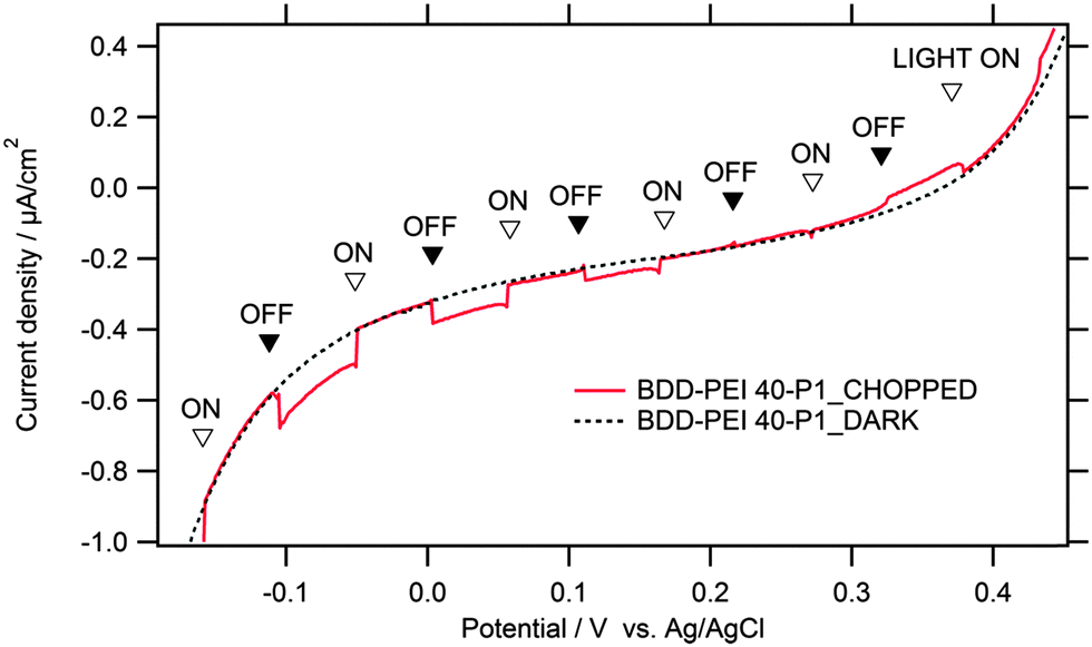 | ||
| Fig. 4 Current density–voltage plot for a BDD electrode sensitized with P1 anchored to the PEI polymer. Electrolyte solution 0.1 M Na2SO4 containing 5 mM dimethylviologen. Illumination with chopped white light from a Xe-lamp (18 mW cm−2). Scan rate 5 mV s−1. | ||
The occurrence of cathodic photocurrent confirms the standard light harvesting mechanism typical for the sensitized p-semiconductors. More specifically, light excitation generates electron–hole pair in the donor-π-bridge-acceptor molecule (P1). Subsequently, the exciton dissociates efficiently, thanks to the favorable molecular structure of P1, and the separated electrons flow to the MV2+ (dimethylviologen) electron carrier which is present in the electrolyte solution. In turn, the photoexcited holes move to the cathode surface and are injected into the valence band of BDD.15,17,18,20,45 It is certainly notable that the polymer carrier (PEI), which is assumed to be an electronic insulator, does not impede the hole-injection from P1 into the diamond electrode. Presumably, the polymer layer is either so thin that the hole tunneling can occur, or the specific structure of PEI–P1 assembly allows certain P1 molecules to approach the surface and contact it directly (cf.Scheme 1).
Fig. 5 shows the details of the response of our electrodes to white light (18 mW cm−2) at various bias voltages. In contrast to the previously discussed experiment, the plot in Fig. 5 is chronoamperometric, i.e. the voltage is constant, and the light is chopped at approx. 20 s intervals. Under the used experimental conditions, the blank BDD shows almost no photocurrents (note slightly faster chopping for better visualization in this case). A closer inspection of Fig. 5 reveals cathodic photocurrents of ca. 5–10 nA cm−2 at the blank BDD, in accord with the earlier study.20 The existence of cathodic photocurrent under sub-bandgap illumination of blank BDD has been previously ascribed to either sp2 impurities or to specific states related to B in the lattice.44 In spite of its unclear origin, the onset of cathodic photocurrent transients allows the determination of flatband potential including its pH-dependence and the effects of surface oxidation.44
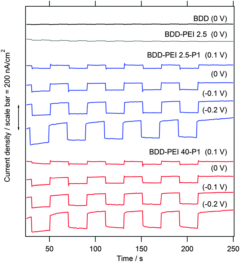 | ||
| Fig. 5 Chronoamperometric plot at various bias voltages (indicated in labels in V vs. Ag/AgCl) for BDD electrodes sensitized with P1 which was anchored through two different PEI polymers. The blank BDD and BDD covered solely with PEI (without P1) were also tested for reference, and the corresponding plots are shown on top of the chart. Electrolyte solution 0.1 M Na2SO4 containing 5 mM dimethylviologen. Illumination with chopped white light (18 mW cm−2). Curves are offset for clarity, but the current density scale is identical in all cases. | ||
The blank BDD covered by a pure PEI polymer (without P1) exhibits small photocurrents similar to the bare BDD. Hence, PEI does not induce any additional photoelectrochemical activity at the BDD surface, but it serves as an intermediate layer for chemical anchoring of P1 (Scheme 1). Furthermore, PEI film is known to decrease the work function of various substrates, such as metals, metal oxides, conducting polymers and graphene.29 Recently, this effect on ITO (indium tin oxide) was used for engineering the electron-extraction interfaces in the perovskite solar cell.46 The lowering of the work function would impede the hole injection, but further discussion of the BDD–PEI interaction is beyond the scope of this work.
The surface sensitization with the PEI–P1 conjugate gives rise to stable photocurrents of ca. 100–150 nA cm−2 at −0.2 V bias. These photocurrents are by an order of magnitude larger than those of the reference blank electrodes (BDD and BDD–PEI) which confirms that sensitization with P1 does occur. Our results compare favorably to those reported recently for the N3-sensitized diamond.18 In spite of the fact that our light intensity is here ca. 8 times smaller, we trace photocurrents, which are ca. 5 times larger than those in ref. 18. Furthermore, our photocurrent response exhibits good stability, which again outperforms the behavior of the N3-sensitized diamond.18 A similar response, both in terms of stability and photocurrent values, was observed for the diamond sensitized by molecular wires with bithiophene and cyclopentadithiophene moieties anchored by Suzuki cross-coupling reactions.20
Fig. 6 shows the plot of incident photon-to-current conversion efficiency (IPCE) of our electrodes. It is defined by the equation:
 | (6) |
| IPCE = ηinj (1–10−Γε) | (7) |
For instance, the N3 dye has ε = 1.27 × 107 cm2 mol−1 at λmax = 530 nm and Γ ≈ 0.55 molecules nm−2 for a monolayer coverage, which provides the theoretical IPCE = 0.27% on a flat surface assuming ηinj = 100% (eqn (7)). The experimental value for a single crystal TiO2 anatase was 0.11%.47 Our BDD films also show quite a flat surface, and we can estimate the roughness factor of ca. 4 from the double-layer capacitance, vide infra. Our experimental IPCE (Fig. 6) is ca. 10 times smaller despite the extinction coefficient of P1 being larger. (P1 has two absorption bands with peaks at 345 and 468 nm, and the extinction coefficient, ε468 = 5.8 × 107 cm2 mol−1.) The difference can be attributed to smaller surface coverage of our electrodes and/or to some other imperfections existing on the diamond surface, but we leave this point open at this stage of our research. Qualitatively, our spectrum in Fig. 6 resembles the IPCE plot for the P1-dye sensitized p-NiO.21 In the latter case, an onset was observed at ca. 650 nm with a broad maximum between 550 to 450 nm extending to 350 nm.21
 | ||
| Fig. 6 IPCE spectrum at −0.2 V bias for B DD electrodes sensitized with P1 anchored via two different PEI polymers. Electrolyte solution 0.1 M Na2SO4 containing 5 mM dimethylviologen. | ||
Our IPCEs and photocurrents are similar to or better than those observed by others for the sensitized BDD electrodes.14–16,18 Furthermore, they compare favorably to values, which were reported in the pioneering studies on the sensitization of TiO2. More specifically, Goodenough et al.48,49 anchored the Ru(bipy)2(bpca) complex (similar to N3) to the flat surface of titania and reported photocurrents of several nA under white light (450 < λ/nm < 650) illumination from a 150 W Xe-lamp.48 Obviously, three decades of research on the optimization of this system provided the current performance of ca. 20 mA cm−2 under 1 sun illumination,1 in spite of the fact that the surface chemistry of the state-of-the-art DSCs and these early systems is quite similar. We believe that the systematic optimization of the solar cells with the BDD photocathodes will bring adequate improvement, too. This optimization should focus on the electrode surface morphology, enhancement of the dye-coverage per projected area, and the fine tuning of interfacial electronic and electrochemical properties. The palette of tasks incudes both the electrolyte/mediator optimization and tuning of the electronic properties (e.g. doping level) of the BDD electrode.
Conclusions
A novel simple and versatile synthetic strategy was developed for the surface modification of boron-doped diamond with a model light-harvesting donor-π-bridge-acceptor molecule (coded P1). The synthetic protocol is based on the use of adsorbed polyethyleneimine (PEI) as a carrier efficiently connecting the diamond surface with the P1 dye.The P1-sensitized diamond exhibits stable cathodic photocurrents of ca. 100–150 nA cm−2 at small cathodic bias (−0.2 V vs. Ag/AgCl) and white light illumination (18 mW cm−2) in aqueous electrolyte solution with dimethylviologen serving as an electron mediator. However, the found IPCEs (≈<0.01%) are still far below those expected for a monolayer of P1 on a flat surface.
This is ascribed to a low roughness factor of the diamond surface causing limited surface coverage by the sensitizer molecules and to the non-optimized electrolyte/mediator system. Nevertheless, our P1–PEI-sensitized diamond exhibits photoelectrochemical performance, which is similar to or better than that reported in most other studies of covalently sensitized diamond electrodes (2008–14) and in the pioneering studies on the n-TiO2 sensitization.
Acknowledgements
This work was supported by the Grant Agency of the Czech Republic (contract No. 13-31783S).References
- A. Hagfeldt, G. Boschloo, L. Sun, L. Kloo and H. Pettersson, Chem. Rev., 2010, 110, 6595 CrossRef CAS PubMed.
- S. Mathew, A. Yella, P. Gao, R. Humphry-Baker, B. F. E. Curdoch, N. A. Astani, I. Tavernelli, U. Rothlisberher, M. K. Nazeeruddin and M. Grätzel, Nat. Chem., 2014, 6, 242 CrossRef CAS PubMed.
- S. Ahmad, E. Guillen, L. Kavan, M. Grätzel and M. K. Nazeeruddin, Energy Environ. Sci., 2013, 6, 3439 CAS.
- L. Kavan, J.-H. Yum and M. Grätzel, Electrochim. Acta, 2014, 128, 349 CrossRef CAS PubMed.
- L. Kavan, J.-H. Yum and M. Grätzel, ACS Appl. Mater. Interfaces, 2012, 4, 6999 CAS.
- L. Kavan, Top. Curr. Chem., 2014, 348, 53 CrossRef.
- H. Tian, J. Oscarsson, E. Gabrielsson, S. K. Eriksson, R. Lindblad, B. Xu, Y. Hao, G. Boschloo, E. M. J. Johansson, J. M. Gardner, A. Hagfeldt, H. Rensmo and L. Sun, Sci. Rep., 2014, 4, 4282 Search PubMed.
- S. Powar, T. Daeneke, M. T. Ma, D. Fu, N. W. Duffy, G. Goetz, M. Weidelener, A. Mishra, P. Baeuerle, L. Spiccia and U. Bach, Angew. Chem., Int. Ed., 2013, 52, 602 CrossRef CAS PubMed.
- A. Nattestad, A. J. Mozer, M. K. R. Fischer, Y. B. Cheng, A. Mishra, P. Bäuerle and U. Bach, Nat. Mater., 2010, 9, 31 CrossRef CAS PubMed.
- I. Zegkinoglou, P. L. Cook, P. S. Johnson, W. Yang, J. Guo, D. Pickup, R. Gonzalez-Moreno, C. Rogero, R. E. Ruther, M. L. Rigsby, J. E. Ortega, R. J. Hamers and F. J. Himpsel, J. Phys. Chem. C, 2012, 116, 13877 CAS.
- S. D. Janssens, P. Pobedinskas, J. Vacik, V. Petrikova, B. Ruttens, J. D'Haen, M. Nesladek, K. Haenen and P. Wagner, New J. Phys., 2011, 13, 083008 CrossRef.
- S. Mori, S. Fukuda, S. Sumikura, Y. Takeda, Y. Tamaki, E. Suzuki and T. Abe, J. Phys. Chem. C, 2008, 112, 16134 CAS.
- C. H. Y. X. Lim, Y. L. Zhong, S. Janssens, M. Nesladek and K. P. Loh, Adv. Funct. Mater., 2010, 20, 1313 CrossRef CAS.
- Y. L. Zhong, A. Midya, Z. Ng, Z. K. Chen, M. Daenen, M. Nesladek and K. P. Loh, J. Am. Chem. Soc., 2008, 130, 17218 CrossRef CAS PubMed.
- Y. L. Zhong, K. P. Loh, A. Midya and Z. K. Chen, Chem. Mater., 2008, 20, 3137 CrossRef CAS.
- C. Petkov, U. Glebe, E. Petkov, A. Pasquarelli, C. Pietzka, M. Veres, L. Himics, R. Merz, W. Kulisch, U. Siemeling, J. P. Reithmaier and C. Popov, Phys. Status Solidi A, 2013, 210, 2048 CrossRef CAS.
- J. Bechter, C. Pietzka, C. Petkov, P. Reintanz, U. Siemeling, C. Popov and A. Pasquarelli, Phys. Status Solidi A, 2014, 211, 2333 CrossRef CAS.
- W. S. Yeap, X. Liu, D. Bevk, A. Pasquarelli, L. Lutsen, M. Fahlman, W. Maes and K. Haenen, ACS Appl. Mater. Interfaces, 2014, 6, 10322 CAS.
- R. E. Ruther, M. L. Rigsby, J. B. Gerken, S. R. Hogendoorn, E. C. Landis, S. S. Stahl and R. J. Hamers, J. Am. Chem. Soc., 2011, 133, 5692 CrossRef CAS PubMed.
- S. W. Yeap, D. Bevk, X. Liu, H. Krysova, A. Pasquarelli, D. Vanderzande, L. Lutsen, L. Kavan, M. Fahlman, W. Maes and K. Haenen, RSC Adv., 2014, 4, 42044 RSC.
- P. Qin, H. Zhu, T. Edvinsson, G. Boschloo, A. Hagfeldt and L. Sun, J. Am. Chem. Soc., 2008, 130, 8570 CrossRef CAS PubMed.
- P. Qin, J. Wiberg, E. A. Gibson, M. Linder, L. Li, T. Brinck, A. Hagfeldt, B. Albinsson and L. Sun, J. Phys. Chem. C, 2010, 114, 4738 CAS.
- P. Ascheulov, J. Sebera, A. Kovalenko, V. Petrak, F. Fendrych, M. Nesladek, A. Taylor, Z. Vlckova-Zivcova, O. Frank, L. Kavan, M. Dracinsky, P. Hubik, J. Vacik, I. Kraus and I. Kratochvilová, Eur. Phys. J. B, 2013, 86, 443 CrossRef.
- Z. Vlckova-Zivcova, O. Frank, V. Petrak, H. Tarabkova, J. Vacik, M. Nesladek and L. Kavan, Electrochim. Acta, 2013, 18, 518 CrossRef PubMed.
- S. Szunerits and R. Boukherroub, J. Solid State Electrochem., 2008, 12, 1205 CrossRef CAS.
- A. Härtl, E. Schmich, J. A. Garrido, J. Hernando, S. C. R. Catharino, S. Walter, P. Feulner, A. Kromka, D. Steinmüller and M. Stutzmann, Nat. Mater., 2004, 3, 736 CrossRef PubMed.
- W. Yang, O. Auciello, J. E. Butler, W. Cai, J. A. Carlisle, J. Gerbi, D. M. Gruen, T. Knickerbocker, T. L. Lasseter, J. Russell, L. M. Smith and R. J. Hamers, Nat. Mater., 2002, 1, 253 CrossRef CAS PubMed.
- X. Wang, P. E. Colavita, J. A. Streifer, J. E. Butler and R. J. Hamers, J. Phys. Chem. C, 2010, 114, 4067 CAS.
- Y. Zhou, C. Fuentes-Hernandez, J. Shim, J. Meyer, A. J. Giordano, H. Li, P. Winget, T. Papadopoulos, H. Cheun, J. Kim, M. Fenoll, A. Dindar, W. Haske, E. Najafabadi, T. M. Khan, H. Sojoudi, S. Barlow, S. Graham, J. L. Bredas, S. R. Marder, A. Kahn and B. Kippelen, Science, 2012, 336, 327 CrossRef CAS PubMed.
- J. Weng, J. Zhang, H. Li, L. Sun, C. Lin and Q. Zhang, Anal. Chem., 2008, 80, 7075 CrossRef CAS PubMed.
- X. Q. Zhang, M. Chen, R. Lam, X. Xu, E. Osawa and D. Ho, ACS Nano, 2009, 3, 2609 CrossRef CAS PubMed.
- A. Fujishima, Y. Einaga, T. N. Rao and D. A. Tryk, Diamond Electrochemistry, Elsevier, Tokyo, 2005 Search PubMed.
- J. Scharpf, A. Denisenko, C. Pietzka and E. Kohn, Diamond Relat. Mater., 2011, 20, 1250 CrossRef CAS PubMed.
- W. Yang, J. E. Butler, J. Russell and R. J. Hamers, Langmuir, 2004, 20, 6778 CrossRef CAS PubMed.
- H. Gu, X. D. Su and K. P. Loh, J. Phys. Chem. B, 2005, 109, 13611 CrossRef CAS PubMed.
- J. A. Garrido, S. Nowy, A. Hartl and M. Stutzmann, Langmuir, 2008, 24, 3897 CrossRef CAS PubMed.
- Y. Pleskov, Y. Evstefeeva, M. D. Krotova, V. Y. Mishuk, V. A. Laptev, Y. Palyanov and Y. Borzdov, J. Electrochem. Soc., 2002, 149, E260–E264 CrossRef CAS PubMed.
- M. D. Krotova, Y. V. Pleskov, A. A. Khomich, V. G. Ralchenko, D. N. Sovyk and V. A. Kazakov, Russ. J. Electrochem., 2014, 50, 101 CrossRef CAS.
- L. Kavan, M. Zukalova, O. Vik and D. Havlicek, ChemPhysChem, 2014, 15, 1056 CrossRef CAS PubMed.
- L. Kavan, N. Tetreault, T. Moehl and M. Grätzel, J. Phys. Chem. C, 2014, 118, 16408 CAS.
- G. Pastor-Moreno and D. J. Riley, Electrochim. Acta, 2002, 47, 2589 CrossRef CAS.
- L. Boonma, T. Yano, D. A. Tryk, K. Hashimoto and A. Fujishima, J. Electrochem. Soc., 1997, 144, L142–L145 CrossRef CAS PubMed.
- Y. G. Lu, S. Turnaer, J. Verbeeck, S. D. Janssens, P. Wagner, K. Haenen and G. Van Tendeloo, Appl. Phys. Lett., 2012, 101, 041907 CrossRef PubMed.
- S. J. Green, L. S. A. Mahe, D. R. Rosseinsky and C. P. Winlove, Electrochim. Acta, 2013, 107, 111 CrossRef CAS PubMed.
- N. C. D. Nath, S. Sarker, A. J. S. Ahammad and J. J. Lee, Phys. Chem. Chem. Phys., 2012, 14, 4333 RSC.
- H. Zhou, Q. Chen, G. Li, S. Luo, T. B. Song, H. S. Duan, Z. Hong, J. You, Y. Liu and Y. Yang, Science, 2014, 345, 542 CrossRef CAS PubMed.
- L. Kavan, M. Grätzel, S. E. Gilbert, C. Klemenz and H. J. Scheel, J. Am. Chem. Soc., 1996, 118, 6716 CrossRef CAS.
- M. P. Dare-Edwards, J. B. Goodenough, A. Hamnett, K. R. Seddon and R. D. Wright, Discuss. Faraday Soc., 1980, 70, 285 RSC.
- S. Anderson, E. C. Constable, M. P. Dare-Edwards, J. B. Goodenough, A. Hamnett, K. R. Seddon and R. D. Wright, Nature, 1979, 280, 571 CrossRef CAS.
Footnote |
| † Electronic supplementary information (ESI) available: X-ray photoelectron and Raman spectra of BDD electrodes. See DOI: 10.1039/c4cp04148h |
| This journal is © the Owner Societies 2015 |