
 Open Access Article
 This Open Access Article is licensed under a
 Creative Commons Attribution 3.0 Unported Licence
Organic metal engineering for enhanced field-effect transistor performance
Raphael
Pfattner
ab,
Concepció
Rovira
ab and
Marta
Mas-Torrent
*ab
aInstitut de Ciència de Materials de Barcelona (ICMAB-CSIC), Campus UAB, 08193 Bellaterra, Spain. E-mail: mmas@icmab.es
bNetworking Research Center on Bioengineering, Biomaterials and Nanomedicine (CIBER-BBN), 08193 Bellaterra, Spain
First published on 28th August 2014
Abstract
A key device component in organic field-effect transistors (OFETs) is the organic semiconductor/metal interface since it has to ensure efficient charge injection. Traditionally, inorganic metals have been employed in these devices using conventional lithographic fabrication techniques. Metals with low or high work-functions have been selected depending on the type of semiconductor measured and, in some cases, the metal has been covered with molecular self-assembled monolayers to tune the work function, improve the molecular order at the interface and reduce the contact resistance. However, in the last few years, some approaches have been focused on utilizing organic metals in these devices, which have been fabricated by means of both evaporation and solution-processed techniques. Higher device performances have often been observed, which have been attributed to a range of factors, such as a more favourable organic/organic interface, a better matching of energy levels or/and to a reduction of the contact resistance. Further, in contrast to their inorganic counterparts, organic metals allow their chemical modification and thus the tuning of the Fermi level. In this perspective paper, an overview of the recent work devoted to the fabrication of OFETs with organic metals as electrodes will be carried out. It will be shown that in these devices not only is the matching of the HOMO or LUMO of the semiconductor with the metal work-function important, but other aspects such as the interface morphology can also play a critical role. Also, recent approaches in which the use of organic charge transfer salts as buffer layers at the metal contacts or on the dielectric or as doping agents of the organic semiconductors that have been used to improve the device performance will be briefly described.
1. Introduction
Organic electronic components are promising candidates for the next generation electronics due to their solution processability, structural versatility by molecular design, and their appealing mechanical properties making flexible electronics a reality.1 One of the most important building blocks of organic electronics is the organic field-effect transistor (OFET), which works as a switch or an amplifier. This device consists of three terminals where the current flowing within the organic semiconductor (OSC) channel from the source to the drain can be tuned using an electric field induced by the gate electrode. Two possible OFET device architectures, bottom-gate bottom-contact (BGBC) and bottom-gate top-contact (BGTC) are shown in Fig. 1.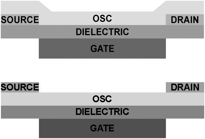 | ||
| Fig. 1 Schematic view of an organic field-effect transistor (OFET). (top) Bottom-gate bottom-contact (BGBC) configuration. (bottom) Bottom-gate top-contact (BGTC) configuration. | ||
To achieve high device performance many different device characteristics have to be considered. In particular, the organic semiconductor/metal interface plays a crucial role since it has a strong influence on the device contact resistance, which needs to be minimized. In an OFET the total resistance can be approximated by three resistances connected in series: contact resistance at the source (RS), channel resistance (RCH) and contact resistance at the drain (RD). Ideally, ohmic source and drain contacts are desired, which implies that the total contact resistance (RC = RS + RD) related to the charge injection and extraction, should be negligible compared to the electrical resistance of the OSC (RCH).2,3
It is also important that the channel resistance scales proportionally with the length of the OFET.4 However, typically this condition is not fulfilled when very short transistor channels are used since then RCH diminishes, implying hence that for shorter channels potential non-ohmic source and drain contacts do have a strong influence on the final device performance.5,6 Moreover, it should be noted that RCH in OFETs is known to decrease at a high absolute source-gate voltage (VG), where more and more charge carriers are accumulated at the dielectric/OSC interface.
One of the parameters that can strongly influence the contact resistance is the employed device architecture.4 The source–drain contacts can be deposited below the OSC as in the case of BGBC configuration (Fig. 1, top) or on the top as in the BGTC architecture (Fig. 1, bottom). Most of the highest mobility values for single crystal OFETs reported in the literature have been found when bottom-contact architectures were employed,7–15 while in the case of thin-film devices top contact geometries tend to give rise to lower contact resistances. The latter is due to metal penetration into the OSC-film when evaporating the top contacts forming an intermixing of both components,16 but also due to the poor morphology of the organic thin-film semiconductors formed when bottom contact is used especially at the edge of the source and drain electrodes.17 Such an effect is also closely related to a higher disorder and related higher density of traps present at the interface of the OSC and the electrodes that inject and extract carriers. However, another issue in the BGTC geometry which goes in the opposite direction, is the highly resistive semiconductor region situated between the contact and the conducting channel which is known to be located in the very few OSC monolayers close to the dielectric interface.18 It has been shown that, in the case of thin-film OFETs, this so called “access resistance” has a strong influence on the extracted field-effect mobility (μFE) and the device performance depending on the thickness of the active layer material.19 On the other hand, the evaporation at high temperature of the source and drain electrodes on the top of single crystal-based OFETs is considered to alter the crystalline order at the surface of the active material and to induce defects.17
Another important aspect that determines the contact resistance is the choice of the metal contact. In organic electronics, most devices are currently fabricated using molecular or polymeric semiconductors where the electrical contacts are formed with inorganic metals.16,20,21 One of the most important parameters in electrode materials is the work function (Φ), which is closely related to the Fermi energy (EF) of the metal, and is defined as the energy needed to move an electron to the vacuum level.22 The choice of the most suitable metal depends on the nature of the OSC. For p-channel OFETs, the Φ value of the source and the drain electrode has to be close to the highest occupied molecular orbital (HOMO) level for efficient charge injection, while for n-channel conduction Φ of the metal electrode has to be close to the lowest unoccupied molecular orbital (LUMO) level. The energetic misalignment will result in the formation of a Schottky barrier increasing the device contact resistance. Therefore, the matching of the molecular energy levels with the metal work function is essential for ensuring an efficient charge injection.
Organic metals have also been explored as electrodes in OFETs, such as poly(3,4-ethylenedioxythiophene)-polystyrene sulfonate (PEDOT:PSS), a doped polymeric material which permits solution processability.23 Other potential candidates are organic charge transfer (CT) salts, with the prime example of tetrathiafulvalene-7,7,8,8-tetracyano-p-quinodimethane ((TTF) (TCNQ)). This CT salt is the first described organic metal that was reported back in 1973.24 Since then, a vast amount of organic metals and organic superconductors derived from an organic donor (D) or an organic acceptor (A), both rich in π-electrons, were reported.25,26 But only recently, it has been shown that such organic conductors might also have a great potential in organic devices,27 not only as contacts but also for improving the overall device performance either by enhancing the OFET mobility or the charge injection efficiency or modifying the threshold voltage. Here, an overview related to the use of CT salts in OFETs will be realized.
2. Charge transfer salts as source and drain electrodes
As mentioned above, conducting CT salts can be employed as source drain contacts in OFETs. Depending on the individual components of the salt and the degree of charge transfer the electrical properties will vary significantly.26,28 Typically, such organic contacts have been fabricated by evaporation, although solution processed techniques to deposit them have also been recently described.2.1. Evaporated CT salts
Two possible strategies to form (TTF)(TCNQ) electrodes by evaporation have been followed: (i) co-evaporation of TTF and TCNQ in one process29,30 or (ii) evaporation of the already formed (TTF)(TCNQ) complex from a single crucible.31 The second approach is possible thanks to the fact that both molecular components have similar sublimation temperatures, and is more commonly found in the literature probably due to a more difficult control of the evaporation parameters when both compounds are evaporated simultaneously from two crucibles in the co-evaporation process.27 However, it should be mentioned that for CT salts containing D and A with very distinct sublimation temperatures, only the co-evaporation of the materials is viable. Furthermore, it has been shown in the co-evaporation process that applying an electric field during the evaporation can lead to a control of the molecular orientation in the films.29One of the highest motivations for using organic electrodes is the possibility of reducing the contact resistance.32–35 (TTF)(TCNQ) source and drain electrodes have been employed in OFETs based on TTF derivatives as OSCs, that is, a similar material to that of the contact electrodes. An analysis of the contact resistance in OFETs with dibenzotetrathiafulvalene (DBTTF) using different source/drain materials was performed by Mori et al.35 They found that the contact resistance decreased in the order Ag > Cu > Au > (TTF)(TCNQ). Also, remarkably, Saito and co-workers reported a very high OFET mobility, exceeding 10 cm2 V−1 s−1, in single crystals of hexamethylenetetrathiafulvalene (HMTTF) when (TTF)(TCNQ) thin-film electrodes were used.34 In contrast, the mobility of these devices when Ag or Au was used as contacts was about 0.12 and 0.02 cm2 V−1 s−1, respectively, which are two or three orders below the values found for the organic contacts.
The reduction in contact resistance with CT salts electrodes has not been proved only for TTF OSCs. For instance, it was also demonstrated in copper-phthalocyanine (CuPc) and pentacene thin films, in which mobilities of more than one order of magnitude were reported when (TTF)(TCNQ) was applied instead of Au.32,33
As previously mentioned, an important issue in top contact electrode fabrication is the heating of the OSC during metal evaporation. In contrast to source/drain electrodes based on Au, which has a high melting temperature (TAu = 1064 °C), (TTF)(TCNQ) thin-films can be thermally evaporated at much lower processing temperatures (T(TTF)(TCNQ) = 110 °C). The application of a lower temperature can suppress the thermal damage to the OSC crystalline surfaces on which the electrodes are deposited during the fabrication process of top-contact devices, which can be an additional cause for the enhanced performance achieved in the devices.34 Haas et al.36 reported high performance dinaphto[2,3-b:2′,3′-f]thieno[3,2-b]-thiophene (DNTT) single crystal OFETs with top contacts in which the mobilities improved from about 0.03 cm2 V−1 s−1 with the use of Au electrodes to up to 8 cm2 V−1 s−1 with (TTF)(TCNQ) electrodes. This was also attributed to the soft preparation procedure of (TTF)(TCNQ) electrodes since when bottom contacts were employed no significant differences were observed between the two types of electrode materials.
Another source which has been described to be a reason for the better performance of the devices with (TTF)(TCNQ) contacts is the better energy matching. It was shown that in the very good electron donor TTF, the usual gold electrodes result in normally on states, while the smaller work-function organic (TTF)(TCNQ) metal leads to a lower off current and threshold voltage.37
(TTF)(TCNQ) has also been demonstrated to be an efficient electrode for n-channel transport.31,35,38,39 For an OSC thin-film of (DBTTF)(TCNQ) for instance, an air-stable n-channel operation was demonstrated when (TTF)(TCNQ) electrodes were used.31,35 Also, (TTF)(TCNQ) was also successfully used as a source and drain contact material in n-channel OFETs based on hexadecafluorophthalocyaninato copper (F16CuPc)38 and dimethyldicyanoquinonediimide (DMDCNQI).39 Furthermore, ambipolar devices were fabricated on the basis of a heterostructure of F16CuPc and copper phthalocyanine (CuPc).38 The high electron injection efficiency in these devices was rationalised considering the presence of a small potential shift on the organic/organic interface compared with the organic/metal interface.
One clear and unique advantage of using organic CT salts as electrodes is that they offer the possibility of energy level tuning by modifying the components of the salt. This was demonstrated by preparing OFETs using (DBTTF)(TCNQ) single crystals as OSC and six different CT salts based on combining different electron donor and electron acceptor molecules. It was observed that depending on the metal Fermi energy the device exhibited p-channel, ambipolar or n-channel transport. Thus, it was possible to chemically tune the metal Fermi level from the conduction-band edge to the valence-band edge of the organic semiconductor (Fig. 2).40 This idea of engineering the organic contacts was also extended to CuPc thin-film transistors.33 After employing different CT complexes, only the salt (TSF)(F2TCNQ) (TSF = tetraselenafulvalene; F2TCNQ = 2,5-difluoroTCNQ) in a top contact geometry in p-channel operation gave rise to mobility values comparable to the ones obtained with Au metals but, remarkably, with considerably smaller contact resistances.
 | ||
| Fig. 2 CT salts used as electrodes in single crystal OFETs to improve charge injection at the contacts. (a) Illustration of the device. (b) Interface band diagram of metal/semiconductor contact in (DBTTF)(TCNQ) single crystal OFET with a variety of organic metal electrodes and (c) The conductive complexes [A]–[F] are drawn as functions of both ionization potentials of the donors (IDP, upper-left axis) and electron affinities of the acceptors (EAA, upper-right axis). Reprinted with permission from ref. 40. Copyright 2006 American Institute of Physics. | ||
An elegant and new concept of self-contact transistors was described using tetramethyltetrathiafulvalene (TMTTF) as the active material and patterned TCNQ on the top to form (TMTTF)(TCNQ) contacts.41 The strategy took into account the following considerations: (i) the same organic molecule can work not only as the active layer in organic transistors but also as the electrode in the form of the CT salt, and (ii) it had been previously shown that at the interface between TTF derivatives and TCNQ single crystals charge transfer occurs with the consequent formation of a conduction channel.42,43 Considering these precedents, TCNQ was evaporated through a shadow mask on a thin film of TMTTF and after an annealing step, the samples were characterized as OFETs. The areas in which the TCNQ was evaporated on the TTF derivative were conducting due to the formation of a CT salt, whereas in the rest of the regions the TMTTF film was used as the active material. Devices with low contact resistance and high performance were achieved, with mobility values of around 0.5 cm2 V−1 s−1, which were of the same order as when evaporated (TTF)(TCNQ) top-contact transistors were fabricated. Later on, the same group used this approach for HMTTF evaporated films also, which had already shown high performance in the past as OSCs.34 Similarly as before, by evaporation of TCNQ through a mask conducting (HMTTF)(TCNQ) top electrodes were formed (Fig. 3a).44 Alternatively, in this case bottom-contact electrodes were also achieved by evaporating the HMTTF OSC on the top of patterned TCNQ films (Fig. 3b). Importantly, the authors also demonstrated the possibility of applying this methodology using a organic flexible substrate (i.e. polyethylenenaphthalate (PEN)), a organic gate contact (i.e. PEDOT:PSS) and an organic gate dielectric (i.e. Parylene C) (Fig. 3c), realizing a full-organic device. The performance achieved in all the device configurations was very similar with mobility values close to 1 cm2 V−1 s−1.
 | ||
| Fig. 3 Self-contact transistor based on CT salt electrodes of (HMTTF)(TCNQ). (a) Top-contact transistor, (b) bottom-contact transistor and (c) all-organic self-contact transistor. Reprinted with permission from ref. 44. Copyright 2014 American Institute of Physics. | ||
All the previous described works have employed (TTF)(TCNQ) electrodes by evaporating the contacts on previously deposited thin film OSC devices or by evaporating the OSC on the top of the patterned organic contacts. Recently, our group has investigated the compatibility of using evaporated (TTF)(TCNQ) electrodes with a solution processed OSC on the top of the electrode array.45 For this study the high performance dithiophenetetrathiafulvalene (DTTTF) OSC was employed as the active material.10,46,47 The HOMO of this material has been calculated to be −4.9 eV,48,49 which is close to the work-function of (TTF)(TCNQ) electrodes (Φ = 4.64–4.78 eV).32,35,38 A solution of DTTTF in either toluene or chlorobenzene (PhCl) was drop-cast on a substrate containing the TTF-TCNQ electrode array and allowed to evaporate slowly. This process resulted in the formation of single crystals, some of which were connected through the organic electrodes. Differences in the OSC crystal/organic metal interface between the devices prepared using the two solvents were already noticeable in the optical microscopy images. However, the crystals grown from toluene were not disturbed on the TTF-TCNQ electrode, while when using PhCl the DTTTF crystals ramified once they were in contact with the organic metal. To obtain a deeper understanding of the formation and the nature of the OSC/organic–metal interface, confocal Raman microscopy as well as atomic force microscopy (AFM) and focused ion beam-scanning electron microscopy (FIB-SEM) were employed. Using these techniques it was proved that devices with toluene grown DTTTF single crystals exhibited a clear separation of the two organic materials, while for the PhCl grown crystals an interpenetration of DTTTF and (TTF)(TCNQ) was found (Fig. 4). Remarkably, the average OFET mobility in devices prepared from PhCl solutions reached a value of 2.5 cm2 V−1 s−1, which was four-fold that obtained from devices prepared from solutions of DTTTF in toluene. These discrepancies in performance were attributed to differences in the contact resistances. Therefore, Kelvin probe microscopy (KPM) experiments were performed to determine the contact resistance by measuring the source–drain current and the distribution of the electrical potential close to the electrodes.50 As shown in Fig. 4 a lower contact resistance was extracted for PhCl processed devices, which stays in agreement with the fact that they were the highest performing OFETs. Thus, it was concluded that preparing single crystal OFETs with organic electrodes using a more polar solution on the top of the (TTF)(TCNQ) leads to a certain re-dissolution of the materials with a subsequent co-precipitation of the two materials. This process does not damage the organic materials but, instead, results in a lower contact resistance in the devices and has a crucial influence on the final device performance. This work highlights, therefore, the importance of the contacts in organic field-effect transistors not only in terms of the alignment of the energy levels but also with respect to the interface morphology.
 | ||
| Fig. 4 (left) Contact resistance (R·W) extracted with the effective potential measured using Kelvin probe microscopy at both the drain (RD, top) and source (RS, bottom) electrodes for a DTTTF single crystal grown from PhCl and toluene at VSD = −5 V. (right, top) Cross-section of single crystal OFETs by an FIB-SEM image with a DTTTF single crystal (bright regions) grown from toluene (A) and from PhCl (B), melting into the TTF-TCNQ electrode (dark regions) on the top of a Si/SiO2 substrate; (right, bottom) SEM image of a DTTTF crystal grown from PhCl on the top of (TTF)(TCNQ). Reprinted with permission from ref. 45. Copyright 2012 Royal Society of Chemistry. | ||
2.2. Solution processed CT salts
CT salts are known to show very poor solubility in common organic solvents, which limits the solution processability of these materials. However, several strategies have been introduced in order to overcome this problem.One approach has focused on preparing (TTF)(TCNQ) nanoparticles stabilised by ionic liquids.51 The nanoparticles were prepared using the precipitation method, which consists in the slow addition of a TTF solution to a TCNQ solution. A substrate with a patterned self-assembled monolayer of hexamethyldisilazane (HMDS) was prepared in order to define hydrophilic and hydrophobic regions. Afterwards, the dispersion of the organic metal nanoparticles in water was deposited on the top resulting in, after a drying step, the formation of thin-films of the CT salt in the hydrophilic areas. Such conducting paths were successfully used as electrodes in pentacene OFETs. Later on, nanoparticles of a variety of CT salts were dispersed in organic solvents and water stabilised with poly(vinylpyrrolidone) (PVP).52 These dispersions could be used to fabricate highly conducting electrodes with high conductivity, of up to 2 kΩ per square, for OFETs. This method provides a route to prepare electrodes based on CT salts that cannot be vacuum evaporated.
A significant breakthrough related to the use of organic CT salts was the development of an inkjet printing technique to pattern the electrodes. Initially, Hiraoka et al.53 reported the use of ink-jet printing to pattern the conductive complex BO9(C14-TCNQ)4 [BO = bis(ethylenedioxy)tetrathiafulvalene and C14-TCNQ = tetradecyltetracyanoquinodimethane]. This salt cannot be thermally evaporated due to decomposition of BO, but, instead, is soluble in some organic solvents. Solutions of the CT salts in DMSO were ink jet printed on substrates. To avoid the formation of the “coffee stain effect” coming from the faster evaporation of solvent at the edges of the droplets and in order to achieve a low film resistivity, the electrode pattern was overprinted 7 times. The resulting organic electrodes were applied in both bottom and top contact pentacene-based OFETs, which exhibited a high performance. However, since most organic CT salts are not soluble, this technique is not suitable for being extended to a large family of materials.
Later on, the same group developed a novel and more versatile technique for patterning CT electrodes. The authors have taken advantage of the relatively good solubility of the individual donor and acceptor molecules to develop a method named “double-shot inkjet printing” (DS-IJP) (Fig. 5, top).54 Dense droplets of inks of the donor and acceptor components are printed individually and once combined they form instantaneously on the substrate high quality metallic films with an electrical conductivity of about 10 S cm−1. Films of (TTF)(TCNQ) as source/drain electrodes prepared by this low cost technique have been used in pentacene thin-film transistors and inverters showing sharp on/off switching at low operational voltages (Fig. 5, bottom).
 | ||
| Fig. 5 OFETs prepared with the double-hot inkjet printing (DS-IJP) technique. (top) Schematic illustration of the printing technique. (bottom) Transfer characteristics of pentacene OFET with various source–drain electrodes: bottom-contact source drain electrodes composed of DS-IJP (TTF)(TCNQ) (red triangles), bottom contact electrodes composed of vacuum-deposited (TTF)(TCNQ) (green triangles), and top-contact Au electrodes (black circles). Reprinted with permission from ref. 54. Copyright 2007 WILEY-VCH Verlag GmbH & Co. KGaA, Weinheim. | ||
With a similar idea, Mukherjee et al.55 have reported a method for fabricating high-performing OFETs with solution processed (TTF)(TCNQ) electrodes by using a capillary based method. A capillary tube, fixed on a Si/SiO2 substrate, was used to define the source and drain electrodes. Subsequently, the soluble TTF and TCNQ precursors were injected individually and once combined on the substrate the conducting CT salt was formed on both sides of the tube. Thus, changing the tube size allows the tuning of the channel dimensions. Using this method, both p- and n-channel devices have been fabricated exhibiting better performance compared to devices with Au electrodes.
3. Charge transfer salts as buffer layers
3.1. At the OSC–dielectric interface
An important part of the OFET device is the dielectric/semiconductor interface, which has to be controlled precisely to obtain high charge transport in the OFET channel. It has been shown in the past that n-octadecyl triethoxysilane (OTS) modified dielectrics often improve the film formation of the organic semiconductor and, thus, enhance the device performance. A similar approach has been reported by using a printed (TTF)(TCNQ) web as a buffer layer between the dielectric and the OSC.56 A very dilute solution of (TTF)(TCNQ) in 1,4-dioxane was employed as the ink, since the formation of continuous conductive thin films was not desired for this application in order to be able to maintain high on/off ratios in the devices. OFETs using different OSCs were fabricated in this way, giving rise to enhanced field-effect mobility of up to several tens of times. This phenomenon was rationalised by the improvement of the inter-grain connection of the semiconductor layer and also by a reduction of the channel length as a consequence that the charge carriers could be partially transported within the semiconductor films but also partially through the (TTF)(TCNQ) nanoweb.3.2. At the contacts
For the improvement of the OSC/metal interface in devices using gold electrodes, often a thiol self-assembled monolayer is grown on the metal contact in BC devices. Alternatively, a thin layer of the acceptor TCNQ, F4TCNQ or a similar acceptor molecule on metal electrodes has also been used by different groups.57,58 In particular, DBTTF OFETs have been reported to employ different organic acceptor layers (TCNQ, F2TCNQ, and F4TCNQ) inserted between the DBTTF and the electrodes.59 In some cases, the device performance was improved with the highest electron affinity complex F4TCNQ and it was explained that this was due to the penetration of the acceptor molecules into the voids of the OSC where a charge transfer process was produced, suppressing the boundary potential.4. Charge transfer complexes for doping the OSC
In most semiconductors the electrical performance is determined to a high degree by modifications of the ideal single crystal due to chemical or structural defects or unintentional doping, which can further induce electrically active sites in the band gap. However, controlled doping might lead to highly reproducible transistors with tuneable device characteristics.In the last few years, a good deal of effort has been placed on adding donor or acceptor molecules to dope n-channel or p-channel organic semiconductors, respectively.60–62 Typically an enhanced conductivity and device performance is achieved with controlled doping, which is accounted for by the formation of free charge carriers and also partly by the consequent filling of the trap states.63–71 Nonetheless, chemical doping can also have other effects such as increasing the stack-ordering and crystallinity72 or influencing the molecular dipoles.61
Lüssem et al.73 reported the first realization of organic inversion transistors and the optimization of organic depletion transistors. The depletion OFETs were fabricated by doping pentacene with the p-dopant F6TCNNQ (2,2′-(perfluoronaphthalene-2,6-diylidene)dimalononitrile). In this configuration the threshold voltage and the on/off ratio can be controlled by the doping concentration and the thickness of the transistor channel. Organic inversion OFETs were prepared by n-doping pentacene with W2(hpp)4 (tetakis(1,3,4,6,7,8-hexahydro-2H-pyrimido[1,2-a]pyrimidinato)ditungsten(II)) and, additionally, doping the contacts with F6TCNNQ to afford injection of minority carriers (i.e. holes, in this case) into the doped transistor channel and the creation of an inversion layer (Fig. 6).
 | ||
| Fig. 6 Organic inversion transistor. (top) Device architecture with a layer of Al2O3 as dielectric, a thin doped layer of pentacene as transistor channel, an intrinsic pentacene layer and doped pentacene source and drain contacts. (bottom) Transfer curves of organic inversion transistors with hole injecting contacts using different doping levels of the OSC: a thin n-doped layer of pentacene with W2(hpp)4, intrinsic pentacene, p-doped pentacene with F6TCNNQ. The inversion transistors have a 6 nm thick n-doped channel. p-Doped depletion transistors are shown for comparison. Reprinted with permission from ref. 73. Copyright 2013 Macmillan Publishers Limited. | ||
Another crucial point to push the device performance in OFETs is the control of the morphological and electrical properties of the transistor channel. In particular, for active materials based on polymeric blend materials, i.e. organic semiconductor with an insulating polymer, moderate doping of the transistor channel was shown to strongly improve the mobility and on/off ratio as well as enhancing the device stability.74 The blends are demonstrated to feature nanometer-scale semiconductor domains with a vertical gradient. Doping the active layer results in the possibility of connecting such semiconductor domains forming pathways within the insulating matrix and, hence, reaching higher on-currents.
5. Conclusions
The use of organic metals as source drain contacts as alternatives to inorganic metals is highly desirable in the field of OFETs. It has been proved that charge transfer salts show a great potential for this purpose since the resulting devices exhibit enhanced performance, mainly due to a reduction of the contact resistance, the softer processing conditions that organic materials require and a more favourable organic/organic interface. Further, although typically CT salts are insoluble materials, a few approaches have also already demonstrated the possibility of applying them using low cost solution-based techniques such as ink-jet printing. It is also important to highlight that organic metals have some unique advantages like the possibility of chemically tuning their work-function almost at will.In addition to the organic contacts, CT salts have also been exploited as buffer layers to improve charge injection and the OSC inter-grain connection, and also as p and n doping agents offering a wide range of possibilities for designing novel devices.
In conclusion, this old class of organic materials that aroused huge scientific interest over forty years ago is bound to now find its place in applications such as the fabrication of advanced organic-field effect transistors.
Acknowledgements
The authors thank the ERC StG 2012-306826 e-GAMES project, the Networking Research Center on Bioengineering, Biomaterials and Nanomedicine (CIBER-BBN), the DGI (Spain) for the project BE-WELL CTQ2013-40480-R and the Generalitat de Catalunya for the project 2014-SGR-17. We acknowledge CSIC for the publication as Open Access in the RSC.Notes and references
- W. Hu, Y.-T. Tao and H. Sirringhaus, Phys. Chem. Chem. Phys., 2012, 14, 14097–14098 RSC.
- N. Tessler and Y. Roichman, Appl. Phys. Lett., 2001, 79, 2987–2989 CrossRef CAS PubMed.
- T. J. Richards and H. Sirringhaus, J. Appl. Phys., 2007, 102, 094510 CrossRef PubMed.
- E. J. Meijer, G. H. Gelinck, E. van Veenendaal, B.-H. Huisman, D. M. de Leeuw and T. M. Klapwijk, Appl. Phys. Lett., 2003, 82, 4576–4578 CrossRef CAS PubMed.
- L. Mariucci, M. Rapisarda, A. Valletta, S. Jacob, M. Benwadih and G. Fortunato, Org. Electron., 2013, 14, 86–93 CrossRef CAS PubMed.
- A. Valletta, A. Daami, M. Benwadih, R. Coppard, G. Fortunato, M. Rapisarda, F. Torricelli and L. Mariucci, Appl. Phys. Lett., 2011, 99, 233309 CrossRef PubMed.
- R. W. I. de Boer, T. M. Klapwijk and A. F. Morpurgo, Appl. Phys. Lett., 2003, 83, 4345–4347 CrossRef CAS PubMed.
- V. C. Sundar, J. Zaumseil, V. Podzorov, E. Menard, R. L. Willett, T. Someya, M. E. Gershenson and J. A. Rogers, Science, 2004, 303, 1644–1646 CrossRef CAS PubMed.
- R. W. I. de Boer, M. E. Gershenson, A. F. Morpurgo and V. Podzorov, Phys. Status Solidi A, 2004, 201, 1302–1331 CrossRef CAS.
- M. Mas-Torrent, M. Durkut, P. Hadley, X. Ribas and C. Rovira, J. Am. Chem. Soc., 2004, 126, 984–985 CrossRef CAS PubMed.
- M. Mas-Torrent, P. Hadley, S. T. Bromley, X. Ribas, J. Tarrés, M. Mas, E. Molins, J. Veciana and C. Rovira, J. Am. Chem. Soc., 2004, 126, 8546–8553 CrossRef CAS PubMed.
- M. Mas-Torrent, P. Hadley, S. T. Bromley, N. Crivillers, J. Veciana and C. Rovira, Appl. Phys. Lett., 2005, 86, 012110 CrossRef PubMed.
- A. L. Briseno, S. C. B. Mannsfeld, X. Lu, Y. Xiong, S. A. Jenekhe, Z. Bao and Y. Xia, Nano Lett., 2007, 7, 668–675 CrossRef CAS PubMed.
- D. H. Kim, D. Y. Lee, H. S. Lee, W. H. Lee, Y. H. Kim, J. I. Han and K. Cho, Adv. Mater., 2007, 19, 678–682 CrossRef CAS.
- A. S. Molinari, H. Alves, Z. Chen, A. Facchetti and A. F. Morpurgo, J. Am. Chem. Soc., 2009, 131, 2462–2463 CrossRef CAS PubMed.
- P. V Pesavento, R. J. Chesterfield, C. R. Newman and C. D. Frisbie, J. Appl. Phys., 2004, 96, 7312–7324 CrossRef PubMed.
- D. Braga and G. Horowitz, Adv. Mater., 2009, 21, 1473–1486 CrossRef CAS.
- A. Shehu, S. Quiroga, P. D'Angelo, C. Albonetti, F. Borgatti, M. Murgia, A. Scorzoni, P. Stoliar and F. Biscarini, Phys. Rev. Lett., 2010, 104, 246602 CrossRef.
- P. V. Pesavento, K. P. Puntambekar, C. D. Frisbie, J. C. McKeen and P. P. Ruden, J. Appl. Phys., 2006, 99, 094504 CrossRef PubMed.
- L. Burgi, T. J. Richards, R. H. Friend and H. Sirringhaus, J. Appl. Phys., 2003, 94, 6129–6137 CrossRef CAS PubMed.
- R. J. Chesterfield, J. C. McKeen, C. R. Newman, C. D. Frisbie, P. C. Ewbank, K. R. Mann and L. L. Miller, J. Appl. Phys., 2004, 95, 6396–6405 CrossRef CAS PubMed.
- C. Weißmantel and C. Hamann, Grundlagen der Festkörperphysik, Johann Ambrosius Barth Verlag, Heidelberg-Leipzig, 1995 Search PubMed.
- E. Becker, R. Parashkov, G. Ginev, D. Schneider, S. Hartmann, F. Brunetti, T. Dobbertin, D. Metzdorf, T. Riedl, H.-H. Johannes and W. Kowalsky, Appl. Phys. Lett., 2003, 83, 4044–4046 CrossRef CAS PubMed.
- J. Ferraris, D. O. Cowan, V. Walatka and J. H. Perlstein, J. Am. Chem. Soc., 1973, 95, 948–949 CrossRef CAS.
- T. Mori, A. Kobayashi, Y. Sasaki, H. Kobayashi, G. Saito and H. Inokuchi, Bull. Chem. Soc. Jpn., 1984, 57, 627–633 CrossRef CAS.
- J. M. Williams, J. R. Ferraro, R. J. Thorn, K. D. Carlson, U. Geiser, H. H. Wang, A. M. Kini and M. H. Wangbo, Organic Superconductors (Including Fullerenes): Synthesis, Structure, Properties, and Theory, Prentice Hall, Englewood Cliffs, New Jersey, 1992 Search PubMed.
- T. Mori, Chem. Lett., 2011, 40, 428–434 CrossRef CAS.
- K. P. Goetz, D. Vermeulen, M. E. Payne, C. Kloc, L. E. McNeil and O. D. Jurchescu, J. Mater. Chem. C, 2014, 2, 3065–3076 RSC.
- N. A. Kato, M. Fujimura, S. Kuniyoshi, K. Kudo, M. Hara and K. Tanaka, Appl. Surf. Sci., 1998, 130–132, 658–662 CrossRef CAS.
- T. Sumimoto, S. Kuniyoshi and K. Kudo, Mol. Cryst. Liq. Cryst. Sci. Technol., Sect. A, 1994, 247, 225–231 CrossRef CAS.
- Y. Takahashi, T. Hasegawa, Y. Abe, Y. Tokura, K. Nishimura and G. Saito, Appl. Phys. Lett., 2005, 86, 063504 CrossRef PubMed.
- K. Shibata, H. Wada, K. Ishikawa, H. Takezoe and T. Mori, Appl. Phys. Lett., 2007, 90, 193509 CrossRef PubMed.
- M. Kraus, S. Richler, A. Opitz, W. Brütting, S. Haas, T. Hasegawa, A. Hinderhofer and F. Schreiber, J. Appl. Phys., 2010, 107, 094503 CrossRef PubMed.
- Y. Takahashi, T. Hasegawa, S. Horiuchi, R. Kumai, Y. Tokura and G. Saito, Chem. Mater., 2007, 19, 6382–6384 CrossRef CAS.
- K. Shibata, K. Ishikawa, H. Takezoe, H. Wada and T. Mori, Appl. Phys. Lett., 2008, 92, 023305 CrossRef PubMed.
- S. Haas, Y. Takahashi, K. Takimiya and T. Hasegawa, Appl. Phys. Lett., 2009, 95, 022111 CrossRef PubMed.
- B. Noda, H. Wada, K. Shibata, T. Yoshino, M. Katsuhara, I. Aoyagi, T. Mori, T. Taguchi, T. Kambayashi, K. Ishikawa and H. Takezoe, Nanotechnology, 2007, 18, 424009 CrossRef CAS PubMed.
- K. Shibata, Y. Watakabe, K. Ishikawa, H. Takezoe, H. Wada and T. Mori, Appl. Phys. Express, 2008, 1, 051801 CrossRef.
- H. Wada, K. Shibata, Y. Bando and T. Mori, J. Mater. Chem., 2008, 18, 4165–4171 RSC.
- Y. Takahashi, T. Hasegawa, Y. Abe, Y. Tokura and G. Saito, Appl. Phys. Lett., 2006, 88, 073504 CrossRef PubMed.
- S. Tamura, T. Kadoya, T. Kawamoto and T. Mori, Appl. Phys. Lett., 2013, 102, 063305 CrossRef PubMed.
- H. Alves, A. S. Molinari, H. Xie and A. F. Morpurgo, Nat. Mater., 2008, 7, 574–580 CrossRef CAS PubMed.
- Y. Takahashi, Y. Nakagawa, K. Hayakawa, T. Inabe and T. Naito, Appl. Phys. Lett., 2012, 101, 103303 CrossRef PubMed.
- S. Tamura, T. Kadoya and T. Mori, Appl. Phys. Lett., 2014, 105, 023301 CrossRef PubMed.
- R. Pfattner, M. Mas-Torrent, C. Moreno, J. Puigdollers, R. Alcubilla, I. Bilotti, E. Venuti, A. Brillante, V. Laukhin, J. Veciana and C. Rovira, J. Mater. Chem., 2012, 1, 16011–16016 RSC.
- M. Leufgen, O. Rost, C. Gould, G. Schmidt, J. Geurts, L. W. Molenkamp, N. S. Oxtoby, M. Mas-Torrent, N. Crivillers, J. Veciana and C. Rovira, Org. Electron., 2008, 9, 1101–1106 CrossRef CAS PubMed.
- R. Pfattner, M. Mas-Torrent, I. Bilotti, A. Brillante, S. Milita, F. Liscio, F. Biscarini, T. Marszalek, J. Ulanski, A. Nosal, M. Gazicki-Lipman, M. Leufgen, G. Schmidt, L. W. Molenkamp, V. Laukhin, J. Veciana and C. Rovira, Adv. Mater., 2010, 22, 4198–4203 CrossRef CAS PubMed.
- M. Mas-Torrent, P. Hadley, X. Ribas and C. Rovira, Synth. Met., 2004, 146, 265–268 CrossRef CAS PubMed.
- S. T. Bromley, M. Mas-Torrent, P. Hadley and C. Rovira, J. Am. Chem. Soc., 2004, 126, 6544–6545 CrossRef CAS PubMed.
- C. Moreno, R. Pfattner, M. Mas-Torrent, J. Puigdollers, S. T. Bromley, C. Rovira, J. Veciana and R. Alcubilla, J. Mater. Chem., 2012, 22, 345–348 RSC.
- D. de Caro, K. Jacob, H. Hahioui, C. Faulmann, L. Valade, T. Kadoya, T. Mori, J. Fraxedas and L. Viau, New J. Chem., 2011, 35, 1315–1319 RSC.
- T. Kadoya, D. de Caro, K. Jacob, C. Faulmann, L. Valade and T. Mori, J. Mater. Chem., 2011, 21, 18421–18424 RSC.
- M. Hiraoka, T. Hasegawa, Y. Abe, T. Yamada, Y. Tokura, H. Yamochi, G. Saito, T. Akutagawa and T. Nakamura, Appl. Phys. Lett., 2006, 89, 173504 CrossRef PubMed.
- M. Hiraoka, T. Hasegawa, T. Yamada, Y. Takahashi, S. Horiuchi and Y. Tokura, Adv. Mater., 2007, 19, 3248–3251 CrossRef CAS.
- B. Mukherjee and M. Mukherjee, Langmuir, 2011, 27, 11246–11250 CrossRef CAS PubMed.
- Y. Li and F. Jian, J. Mater. Chem. C, 2014, 2, 1413–1417 RSC.
- C. Vanoni, S. Tsujino and T. A. Jung, Appl. Phys. Lett., 2007, 90, 193119 CrossRef PubMed.
- C. Mitsui, T. Okamoto, M. Yamagishi, J. Tsurumi, K. Yoshimoto, K. Nakahara, J. Soeda, Y. Hirose, H. Sato, A. Yamano, T. Uemura and J. Takeya, Adv. Mater., 2014, 26, 4546–4551 CrossRef CAS PubMed.
- T. Yamada, T. Hasegawa, M. Hiraoka, H. Matsui, Y. Tokura and G. Saito, Appl. Phys. Lett., 2008, 92, 233306 CrossRef PubMed.
- Y. Zhang, B. de Boer and P. W. M. Blom, Adv. Funct. Mater., 2009, 19, 1901–1905 CrossRef CAS.
- T. Hählen, C. Vanoni, C. Wäckerlin, T. A. Jung and S. Tsujino, Appl. Phys. Lett., 2012, 101, 033305 CrossRef PubMed.
- H. Méndez, G. Heimel, A. Opitz, K. Sauer, P. Barkowski, M. Oehzelt, J. Soeda, T. Okamoto, J. Takeya, J.-B. Arlin, J.-Y. Balandier, Y. Geerts, N. Koch and I. Salzmann, Angew. Chem., 2013, 52, 7751–7755 CrossRef PubMed.
- J. H. Oh, P. Wei and Z. Bao, Appl. Phys. Lett., 2010, 97, 243305 CrossRef PubMed.
- Y. Qi, S. K. Mohapatra, S. Bok Kim, S. Barlow, S. R. Marder and A. Kahn, Appl. Phys. Lett., 2012, 100, 083305 CrossRef PubMed.
- B. D. Naab, S. Himmelberger, Y. Diao, K. Vandewal, P. Wei, B. Lüssem, A. Salleo and Z. Bao, Adv. Mater., 2013, 25, 4663–4667 CrossRef CAS PubMed.
- T. H. Lee, B. Lüssem, K. Kim, G. Giri, Y. Nishi and Z. Bao, ACS Appl. Mater. Interfaces, 2013, 5, 2337–2341 CAS.
- E. Lim, B.-J. Jung, M. Chikamatsu, R. Azumi, Y. Yoshida, K. Yase, L.-M. Do and H.-K. Shim, J. Mater. Chem., 2007, 17, 1416–1420 RSC.
- S. Nam, J. Kim, H. Lee, H. Kim, C.-S. Ha and Y. Kim, ACS Appl. Mater. Interfaces, 2012, 4, 1281–1288 CAS.
- P. Wei, J. H. Oh, G. Dong and Z. Bao, J. Am. Chem. Soc., 2010, 132, 8852–8853 CrossRef CAS PubMed.
- J. Soeda, Y. Hirose, M. Yamagishi, A. Nakao, T. Uemura, K. Nakayama, M. Uno, Y. Nakazawa, K. Takimiya and J. Takeya, Adv. Mater., 2011, 23, 3309–3314 CrossRef CAS PubMed.
- L. Ma, W. H. Lee, Y. D. Park, J. S. Kim, H. S. Lee and K. Cho, Appl. Phys. Lett., 2008, 92, 063310 CrossRef PubMed.
- Z. Wei, H. Xi, H. Dong, L. Wang, W. Xu, W. Hu and D. Zhu, J. Mater. Chem., 2010, 20, 1203–1207 RSC.
- B. Lüssem, M. L. Tietze, H. Kleemann, C. Hoßbach, J. W. Bartha, A. Zakhidov and K. Leo, Nat. Commun., 2013, 4, 2775 Search PubMed.
- G. Lu, J. Blakesley, S. Himmelberger, P. Pingel, J. Frisch, I. Lieberwirth, I. Salzmann, M. Oehzelt, R. Di Pietro, A. Salleo, N. Koch and D. Neher, Nat. Commun., 2013, 4, 1588 CrossRef PubMed.
| This journal is © the Owner Societies 2015 |